评估板DSP56311EVM.
第四章:DSP的开发环境

C 编译器的优化
C编译器的效率取决于所作的优化的 范围和数量。TMS320的C编译器能 作很宽范围的多种优化,从而改善 其编译所得代码的效率。 TMS320的C编译器所作的优化分为 适用于所有处理器的通用优化和针 对特定片种的专门优化
汇编语言工具
TMS320的汇编语言工具是一个软件 包,其中包括: 汇编器 连接器 归档器 交叉引用列表器 十六进制转换公用程序
第五章 DSP的开发 环境与工具
一般估计,一个嵌入式系统, 开发的80%的努力,以及系统的 80%的复杂程度,取决于软件。 因此,设计人员在为实时系统 选择处理器时,都极为看重先进的、 易于使用的开发环境与工具。
DSP的开发环境和工具
代码生成工具(编译器,连 接器,优化C编译器,转换工 具等) 系统集成及调试环境与工具 实时操作系统
用户实验代码
DES PC插卡
DES的图形化中文界面
信号源
虚拟示波器
虚拟频谱仪
VC5402实验板
VC5402实验板
1. 2. 3. 4. 5. 6. 7. 8. 9. 两路独立的A/D和D/A通道 HPI接口引脚 32KB启动FLASH RAM(占用地址0x8000-0x0FFFF) 16K外部数据存储器(占用地址0x4000-0x7FFF) 32K外部程序存储器(占用地址0x38000-0x3FFFF) 方便灵活的外部电源输入(+6v - +18v) McBSPs串口引脚 TMS320VC5402-PGE100 JTAG引脚
集成化的DSP开发环境CCS
主机和目标机之间的实时数据交换 (RTDX) 实时分析和数据可视化 目前可用于WIN95、 WIN98和NT4等 多种操作系统。
基于WIN的图形化界面
i.MX 6SoloLite 评估板快速入门指南说明书

MCIMXHDMICARD.i.MX 6SoloLite Evaluation Kit Quick Start Guidei.MX 6SoloLite Evaluation KitQuick Start GuideAbout the i.MX 6SoloLite Evaluation KitThe i.MX 6SoloLite evaluation kit (EVK) offers a solid platform to evaluate thei.MX 6 series single-core applications processor built on ARM® Cortex®-A9 technology as well as a reference for future designs. Key features of this platform include:• i.MX6SL single Cortex-A9core operating up to 1 GHz• 1 GB LPDDR2 (400 MHz)• SPI NOR• SD socket for external devices• SD socket for boot code• SD socket for Wi-Fi® and accessories • eMMC expansion footprint• Audio codec • EPDC expansion port• Parallel display port• Port for CSI CMOS sensor (camera)• SIM card slotButton matrix• Ethernet• Lithium battery charger• USB host, USB OTG and USB to UART ports2 Getting StartedThe i.MX 6SoloLite EVK includes the following items:• Board: MCIMX6SLEVK• Cables: Micro USB-B-2-USB-Type A male, V2.0• Power supply: 100/240 V input, 5 V, 2.4 A output W/AC adaptor• Documentation: Quick Start Guide (this document)• Two SD cards: Programmed Android™34Figure 1: Front side of i.MX 6SoloLite EVK (top)Quick Start GuideOvervoltage LEDMain PowerLEDPMIC on LEDMicrophoneParallelDisplayPortSIM Card SlotEPDCExpansionPortPort for CSICMOS Sensor(Camera)ButtonMatrixGet to Know the i.MX 6SoloLite EVK5Figure 2: Back side of i.MX 6SoloLite EVK (bottom)5 V PowerJackMini PCIe(Only USB connection is supplied for Mini PCIe connector)USB HostUSB OTGLi Cell ConnectorsOn/Off SwitchEthernet Connector JTAG Connector Boot ModeSelection Switch USB to UARTConnectorBootSelection SwitchesHeadphone ConnectorSpeaker OuteMMC Expansion FootprintSD Socket for Wi-Fi and SD Accessories(SD3)SD Socket for Primary External Card Slot (SD1)SD Socket for Boot Code (SD2)Quick Start Guide Setting Up the Board1Insert SDCardInsert the supplied SD card into the SD2 card slot.2Set Up BootSwitchesBy default, boot switches are configured to boot from SD2. If any other boot source is desired, boot switches have to be configured according to Table 1. 3Connect USB toUART CableConnect from USB to UART port (J26) using a micro USB cable to PC. Once the PC recognizes the virtual USB to UART device, it can be seen it in your PC Device Manager list.Serial port configuration: 115.2 Kbaud, 8 data bits, 1 stop bit, no parity.Note: The PC needs a driver to enable a virtual COM port through the PC USB port. Visit /drivers/vcp.htm to download the correct driver.4Connect EPDC orParallel DisplayConnect by means of the IMXEBOOKDC3-E board, which has to be connected to J12 and J13. For more information about this board, please visit .5ConnectPower DisplayConnect 5 V power supply into power jack J6 and set SW14 to the On position.6 Setting Up the Board (cont.)The i.MX 6SoloLite EVK is compatible with the following daughter cards through the LCD extension slot:• MCIMX28LCD—LCD daughter card*• MCIMXHDMICARD—HDMI daughter card• IMXEBOOKDC3-E—EPD daughter card* E VK does not natively support the resistive touchscreen on the LCD and HDMI cards. Use a USBmouse to navigate when using the LCD or HDMI cards. Touch is supported on the EPDC card.7Quick Start GuideThe Android BSP is provided on two different SD cards, depending upon the display daughter card used.LCD/HDMI SD Card for Booting AndroidThe default boot mode configures the system to display the UI on the MCIMX28LCD (sold separately).To change the default configuration and enable the MCIMXHDMICARD daughter card (sold separately), hit any key to stop u-boot from proceeding. Once prompt is visible, the u-boot can be configured as follows:For LCD boot up, type the following commands (as one line):setenv bootargs console=ttymxc0,115200 init=/initandroidboot.console=ttymxc0 panel=lcdsaveenvresetFor HDMI boot up, type the following commands (as one line):setenv bootargs console=ttymxc0,115200 init=/initandroidboot.console=ttymxc0 panel=hdmisaveenvresetEPDC SD Card for Booting AndroidThe default settings should be used and no change is needed.8 Boot Options and Switch ConfigurationTable 1: Boot OptionsS1_2S1_1BOOT_MODE1BOOT_MODE0Boot from fuses00Serial downloader D01Internal boot10Reserved11Table 2: SW3 ConfigurationSW3_8SW3_7SW3_6SW3_5SW3_4SW3_3SW3_2SW3_1BT_CFG1_0BT_CFG1_1BT_CFG1_2BT_CFG1_3BT_CFG1_4BT_CFG1_5BT_CFG1_6BT_CFG1_7 SD1******010SD2D******010SD3******010SD4******010 eMMC X X***110SPI NOR X X X X1100X None specifiedDefault configuration* Switch needs to be configured for high or low depending on the application needs.Please check reference manual for boot configuration options.** 1 = power cycle on power-up via SDa_RST_B (SD3_RST). 0 = no power cycle910Quick Start GuideBoot Options and Switch Configuration (cont.)Table 4: SW5 ConfigurationSW5_8SW5_7SW5_6SW5_5SW5_4SW5_3SW5_2SW5_1BT_CFG4_0BT_CFG4_1BT_CFG4_2BT_CFG4_3BT_CFG4_4BT_CFG4_5BT_CFG4_6BT_CFG4_7SD1XX X X X X X X SD2DX X X X X X X X SD3X X X X X X X X SD4X X X X X X X X eMMC X X X X X X X X SPI NOR1XXTable 3: SW4 ConfigurationSW4_8SW4_7SW4_6SW4_5SW4_4SW4_3SW4_2SW4_1BT_CFG2_0BT_CFG2_1BT_CFG2_2BT_CFG2_3BT_CFG2_4BT_CFG2_5BT_CFG2_6BT_CFG2_7SD1*X X 001**SD2D*X X 101**SD3*X X 011**SD4*X X 111**eMMC ***10011SPI NORXXXXXXXXXNone specified Default configuration* Switch needs to be configured for high or low depending on the application needs.Please check reference manual for boot configuration options.** 1 = power cycle on power-up via SDa_RST_B (SD3_RST). 0 = no power cycleJumper and Solder Short ConfigurationTable 5: Jumper and Solder Short ConfigurationReference Shunt Installation FunctionJ161–2Use pins 1 and 2 to connect an external charger 2–3Shunt 2–3 to experiment with USB charging Open D No chargerJ171–2D 5 V rail supplied by PMIC (600 mA limited) 2–3 5 V rail supplied from wall adapterJ181–2Mini-PCIe connector J8 supply voltage connected Open D Mini-PCIe connector J8 supply voltage unconnectedSH121–2D MX_USB_HOST_D_P connected to USB type A connector 2–3J10-USB_HOST_D_PMX_USB_HOST_D_P connected to PCIE_USB_HOST_D_PSH131–2D MX_USB_HOST_D_N connected to USB type A connector 2–3J10-USB_HOST_D_NMX_USB_HOST_D_N connected to PCIE_USB_HOST_D_NSW141–2D0 2–3Default configurationTips and PrecautionsThe i.MX 6SoloLite includes an overvoltage protection circuit that will disconnect the power supply from the system by opening transistor Q1 in case the supply voltage exceeds 5.5 V. The user must take into account this is the maximum voltage that can be plugged into J6.Further Documentation• MX6SL EVK schematics• MX6SL EVK BOM• MX6SL EVK gerber files• MX6SL EVK reference manualComplete documentation is availableat /6SLEVK.11SupportVisit the i.MX community at . WarrantyVisit /warranty for completewarranty information.For more information, visit /iMX6series Freescale and the Freescale logo are trademarks of Freescale Semiconductor, Inc., Reg. U.S. Pat. & Tm. Off. All other product or service names are the property of their respective owners. ARM and Cortex are registered trademarks of ARM Limited (or its subsidiaries) in the EU and/or elsewhere. All rights reserved. © 2012, 2014 Freescale Semiconductor, Inc.Doc Number: IMX6SLEVKQSG REV 2 Agile Number: 926-27452 REV BMCIMXHDMICARD.。
maxim-max7311evkit-evkit-评估板-说明书

Evaluates: MAX7311MAX7311 Evaluation KitGeneral DescriptionThe MAX7311 evaluation kit (EV kit) provides a proven design to evaluate the MAX7311 I 2C-compatible 16-bit I/O port expander, with each port configurable as input or push-pull output. The EV kit also includes Windows ® 2000/XP/Vista ®-compatible software that provides a simple graphical user interface (GUI) for exercising the features of the MAX7311. The MAX7311 EV kit PCB comes with a MAX7311ATG+ installed.Features●Windows 2000/XP/Vista (32-Bit)-CompatibleEvaluation Software ●USB-PC Connection (Cable Included) ●USB Powered●Configurable Input or Push-Pull Output ●Proven PCB Layout ●Fully Assembled and Tested ●RoHS Compliant●On-Board Pushbutton Switches●On-Board LEDs for Demonstrating the Push-PullCapabilities of the GPIOs19-4151; Rev 1; 10/20Windows and Windows Vista are registered trademarks of Microsoft Corp.#Denotes RoHS compliant*EP = Exposed pad.PART TYPE MAX7311EVKIT#EV KitDESIGNATION QTY DESCRIPTIONC1, C12, C14310μF ±20%, 16V X5R ceramic capacitors (1206)Murata GRM31CR61C106M C2, C3222pF ±5%, 50V C0G ceramic capacitors (0603)Murata GRM1885C1H220J C410.033μF ±10%, 16V X5R ceramic capacitor (0603)Taiyo Yuden EMK107BJ333KA C5–C10, C17, C18, C2090.1μF ±10%, 16V X7R ceramic capacitors (0603)TDK C1608X7R1C104K C11, C13, C131μF ±10%, 16V X5R ceramic capacitors (0603)TDK C1608X5R1C105K C15, C16210pF ±5%, 50V C0G ceramic capacitors (0603)Murata GRM1885C1H100J D1, D3, D5, D7, D9, D11, D13, D158Green LEDs (0603)D2, D4, D6, D8, D10, D12, D14, D168Red LEDs (0603)J11USB series type-B right-angle PC-mount receptacleDESIGNATION QTY DESCRIPTIONJU0, JU1, JU235-pin headers JU3, JU4, JU533-pin headers L11Ferrite beadR1, R2227Ω ±5% resistors (0603)R3, R17, R18,R194 1.5kΩ ±5% resistors (0603)R51 2.2kΩ ±5% resistor (0603)R6, R36, R37310kΩ ±5% resistors (0603)R101169kΩ ±1% resistor (0603)R111100kΩ ±1% resistor (0603)R12–R160Not installed; resistors—short (PC trace) (0603)R4, R20–R3517470Ω ±5% resistors (0603)S1, S22Pushbutton switches U11I/O port expander (24 TQFN-EP*)Maxim MAX7311ATG+U21Adjustable output LDO regulator (5 SC70)Maxim MAX8512EXK+T U31LDO regulator (5 SC70)Maxim MAX8511EXK25+T U41UART-to-USB converter (32 TQFP)FTDI FT232BLOrdering InformationComponent ListClick here to ask about the production status of specific part numbers.Quick StartRecommended EquipmentBefore beginning, the following equipment is needed:●MAX7311 EV kit (USB cable included)● A user-supplied Windows 2000/XP/Vista-compatiblePC with a spare USB portNote: In the following sections, software-related items are identified by bolding. Text in bold refers to items directly from the EV kit software. Text in bold and underlined refers to items from the Windows operating system.ProcedureThe MAX7311 EV kit is fully assembled and tested. Follow the steps below to verify board operation:1) Visit /evkit-software todownload the latest version of the EV kit software, 7311Rxx.ZIP. Save the EV kit software to a temporary folder and uncompress the ZIP file.2) Install the EV kit software on your computer by run-ning the INSTALL.EXE program inside the temporary folder. The program files are copied and icons are created in the Windows Start | Programs menu.3) Verify that all jumpers (JU0–JU5) are in their defaultpositions, as shown in Table 1.4) Connect the USB cable from the PC to the EV kitboard. A New Hardware Found window pops up when installing the USB driver for the first time. If youdo not see a window that is similar to the one describedabove after 30 seconds, remove the USB cable from the board and reconnect it. Administrator privileges are required to install the USB device driver on Windows. 5) Follow the directions of the Add New HardwareWizard to install the USB device driver. Choose the Search for the best driver for your device option.Specify the location of the device driver to be C:\Program Files\MAX7311 (default installation directory) using the Browse button. During device driver installation, Windows may show a warning message indicating that the device driver Maxim usesdoes not contain a digital signature. This is not an error condition and it is safe to proceed with instal-lation. Refer to the USB_Driver_Help.PDF document included with the software for additional information. 6) Start the MAX7311 EV kit software by opening its iconin the Start | Programs menu. The EV kit software main window appears, as shown in Figure 1.7) Wait approximately five seconds for the program toautomatically detect the slave address (0x40) of the MAX7311 in the I2C Addresses group box.8) Set I/O0–I/O7 to outputs by selecting all Outputradio buttons in the Configuration group box.9) Verify that all red LEDs are brightly lit.*EP = Exposed pad.Note: Indicate that you are using the MAX7311 when contacting these component suppliers.DESIGNATION QTY DESCRIPTIONU5193C46 type 3-wire EEPROM (8 SO) Atmel AT93C46A-10SU-2.7U61Microcontroller (68 QFN-EP*) Maxim MAXQ2000-RAX+Y1116MHz crystalCitizen Finedevice Crystals HCM4916000000ABJTY216MHz crystalCitizen Finedevice Crystals HCM496000000ABJTY30Not installed, crystal—6Shunts—1USB high-speed A-to-B cables, 6ft —1PCB: MAX7311 Evaluation Kit+SUPPLIER PHONE WEBSITE CitizenFinedeviceCo. Ltd.(Crystal)+81-267-31-1111cfd.citizen.co.jp/englishMurataElectronicsAmerica, Inc. Taiyo TDK SUPPLIER WEBSITEINSTALL.EXE Installs the EV kit files on your computer MAX7311.EXE Application programFTD2XX.INF USB device driver fileUNINST.INI Uninstalls the EV kit software USB_Driver_Help.PDF USB driver installation help fileComponent List (continued)Component SuppliersMAX7311 EV Kit FilesDetailed Description of SoftwareTo start the MAX7311 EV kit software, double-click on the MAX7311 EV kit icon that is created during installation. The GUI main window appears, as shown in Figure 1. Port 1 and Port 2 TabsThe Port 1 tab sheet shown in Figure 1 controls all of the registers for I/O0–I/O7 of the MAX7311. In the Configuration group box, the user can set the I/O port as an input or output by selecting the adjacent Input or Output radio buttons.In the Input Port group box, press the Read button to read the input port status.Check the desired checkboxes and press the Write button in the Polarity Inversion group box to invert the polarity of the corresponding port pins. Uncheck the checkboxes and press the Write button to obtain the default polarity of the corresponding port pins.Figure 1. MAX7311 EV Kit Software Main Window (Port 1 Tab)Check or uncheck the desired checkboxes and press the Write button in the Output Port group box to write the port settings to the MAX7311.The Port 2 tab sheet shown in Figure 2 contains the same functions as the Port 1 tab sheet to control the registers for I/O8–I/O15.Bus Timeout CheckboxCheck the Bus Timeout checkbox to enable the bus-timeout function.Interrupt Status Group BoxThe Interrupt Status group box shows the current status of the MAX7311 INT pin (active-low latching-transition-detection interrupt output).Figure 2. MAX7311 EV Kit Software Main Window (Port 2 Tab)I 2C Addresses Group BoxThe I 2C slave address of the MAX7311 depends on the jumper settings of JU0, JU1, and JU2. The I2C Addresses drop-down list automatically detects the MAX7311’s I 2C slave address when the GUI software starts. The default I 2C slave address, when the EV kit is shipped, is 0x40.Reconnect ButtonIf the jumper settings of JU0, JU1, and JU2 change, press the Reconnect button to automatically detect the new I 2C slave address of the MAX7311.Detailed Description of HardwareThe MAX7311 has 16 I/Os, configurable as push-pull outputs or inputs. The MAX7311 EV kit board provides a proven layout for evaluating the MAX7311. The EV kit comes with a MAX7311ATG+ installed.I 2C Address ConfigurationThe combinations of shunt position of jumpers JU0,JU1, and JU2 determine the I 2C slave address of theMAX7311 device. Refer to the MAX7311 IC data sheet for appropriate settings.Output Evaluations of I/OsThere are eight red LEDs and eight green LEDs on the EV kit to demonstrate the push-pull capability of the I/Os. When an I/O is configured as an output and the logic level is high, the corresponding red LED will be on and the green LED will be off. If the logic level is low, the corre-sponding green LED will be on and the red LED will be off.Input Evaluations of I/OsTwo pullup resistors and two pushbuttons are connected to I/O8 and I/O9 of the MAX7311. Press pushbutton S2 to drive I/O8 low and press pushbutton S1 to drive I/O9 low.User-Supplied Power SupplyBy default, the MAX7311 EV kit is powered by USB. To use the user-supplied power supply, place a shunt on pins 2-3 of JU5, cut the trace between pins 1-2 of JU5, and connect a 2.5V to 3.3V power supply to the VIN pad.User-Supplied I 2C InterfaceTo use the MAX7311 EV kit with a user-supplied I 2C interface, install shunts on pins 2-3 of JU3 and JU4. Connect SDA, SCL, and GND lines from the user- supplied I 2C interface to the SDA, SCL, and GND pads on the MAX7311 EV kit. Place a shunt on pins 2-3 of JU5, cut the trace between pins 1-2 of JU5, and connect a 2V to 5.5V power supply to the VIN pad.Table 1. MAX7311 EV Kit Jumper Descriptions (JU0–JU5)*Default position JUMPERSSHUNT POSITIONDESCRIPTIONJU01-2Connects AD0 to SCL 1-3Connects AD0 to SDA 1-4*Connects AD0 to GND 1-5Connects AD0 to VCC JU11-2Connects AD1 to SCL 1-3Connects AD1 to SDA 1-4*Connects AD1 to GND 1-5Connects AD1 to VCC JU21-2Connects AD2 to SCL 1-3Connects AD2 to SDA 1-4*Connects AD2 to GND 1-5Connects AD2 to VCCJU31-2MAX7311 SCL signal connected to on-board microcontroller 2-3Connects user-supplied SCL signal to the on-board SCL pad JU41-2*MAX7311 SDA signal connected to on-board microcontroller 2-3Connects user-supplied SDA signal to the on-board SDA padJU51-2*MAX7311 V+ is set to the on-board 3.3V supply powered from the USB port 2-3Connects user-supplied external supply to the VIN padFigure 3a. MAX7311 EV Kit Schematic (Sheet 1 of 2)Figure 3b. MAX7311 EV Kit Schematic (Sheet 2 of 2)1.0”Figure 4. MAX7311 EV Kit Component Placement Guide—Component SideFigure 5. MAX7311 EV Kit PCB Layout—Component SideFigure 6. MAX7311 EV Kit PCB Layout—Solder SideMaxim Integrated cannot assume responsibility for use of any circuitry other than circuitry entirely embodied in a Maxim Integrated product. No circuit patent licenses are implied. Maxim Integrated reserves the right to change the circuitry and specifications without notice at any time.Maxim Integrated and the Maxim Integrated logo are trademarks of Maxim Integrated Products, Inc.© 2020 Maxim Integrated Products, Inc. │ 11Evaluates: MAX7311MAX7311 Evaluation Kit REVISION NUMBER REVISION DATEDESCRIPTION PAGES CHANGED 05/08Initial release —110/20Updated Ordering Information , Features, Component List, Component Suppliers,and Figure 41, 2, 8Revision HistoryFor pricing, delivery, and ordering information, please visit Maxim Integrated’s online storefront at https:///en/storefront/storefront.html.。
INMP441 MEMS麦克风评估板说明书
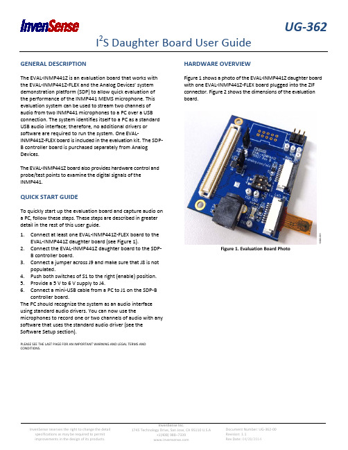
UG-362 I2S Daughter Board User GuideGENERAL DESCRIPTIONThe EVAL-INMP441Z is an evaluation board that works with the EVAL-INMP441Z-FLEX and the Analog Devices’ system demonstration platform (SDP) to allow quick evaluation of the performance of the INMP441 MEMS microphone. This evaluation system can be used to stream two channels of audio from two INMP441 microphones to a PC over a USB connection. The system identifies itself to a PC as a standard USB audio interface; therefore, no additional drivers or software are required to run the system. One EVAL-INMP441Z-FLEX board is included in the evaluation kit. The SDP-B controller board is purchased separately from Analog Devices.The EVAL-INMP441Z board also provides hardware control and probe/test points to examine the digital signals of theINMP441.QUICK START GUIDETo quickly start up the evaluation board and capture audio on a PC, follow these steps. These steps are described in greater detail in the rest of this user guide.1.Connect at least one EVAL-INMP441Z-FLEX board to theEVAL-INMP441Z daughter board (see Figure 1).2.Connect the EVAL-INMP441Z daughter board to the SDP-B controller board.3.Connect a jumper across J9 and make sure that J8 is notpopulated.4.Push both switches of S1 to the right (enable) position.5.Provide a 5 V to 6 V supply to J4.6.Connect a mini-USB cable from a PC to J1 on the SDP-Bcontroller board.The PC should recognize the system as an audio interface using standard audio drivers. You can now use the microphones to record one or two channels of audio with any software that uses the standard audio driver (see the Software Setup section).PLEASE SEE THE LAST PAGE FOR AN IMPORTANT WARNING AND LEGAL TERMS AND CONDITIONS.HARDWARE OVERVIEWFigure 1 shows a photo of the EVAL-INMP441Z daughter board with one EVAL-INMP441Z-FLEX board plugged into the ZIF connector. Figure 2 shows the dimensions of the evaluation board.Figure 1. Evaluation Board Photo 1432-1InvenSense reserves the right to change the detail specifications as may be required to permitimprovements in the design of its products.InvenSense Inc.1745 Technology Drive, San Jose, CA 95110 U.S.A+1(408) 988–7339Document Number: UG-362-00Revision: 1.1Rev Date: 04/28/2014UG-362Dimensions shown in millimetersSETTING UP THE EVALUATION BOARDHARDWARE SETUP PowerThe EVAL-INMP441Z board is powered with a single 5 V to 6 V supply from either Barrel Connector J4 or Pin Header J5. The dc supply connected to J4 should be positive-tip. The micro-phones are configured to run with a single 1.8 V supply, but the supply can be set to either 2.5 V or 3.3 V by mounting a 0 Ω resistor on R17 or R11, respectively, and removing R18.LED D1 is illuminated when the board is powered on. With V DD = 1.8 V, the LED is only faintly lit.Power is supplied to the EVAL-INMP441Z-FLEX board through Voltage Regulator U5.The power supply connected to the EVAL-INMP441Z board also powers the SDP-B controller board through Connector J3. The microphone board requires only a few milliamps of current, but the SDP-B controller board requires up to 200 mA at 5 V.JumpersThe J8 and J9 jumper headers on the EVAL-INMP441Z board set the clock source and select the boot code.Header J8 does not need to be shorted with a jumper for the default clocking configuration. When J8 is populated, the 3.072 MHz crystal on the EVAL-INMP441Z board generates the master clock for the SPORT interface of the Blackfin® processor. By default, however, the microphone clocks are generated on the Blackfin processor.Header J9 selects the source of the code to boot the Blackfin processor on the SDP-B controller board. To use theevaluation system to stream USB audio to a PC, a jumper must be shorted across Header J9. Without the jumperpresent, the Blackfin processor boots the standard SDP code and does not perform USB streaming audio.These settings for J8 and J9 are illustrated in Figure 3.Figure 3. Top View of EVAL-IN MP441Z Board with Default Switchand Jumper Settings10432-00210432-003Document Number: UG-362--00 Page 2 of 9Revision: 1.1Rev Date: 04/28/2014UG-362SwitchesSwitch Block S1 has two SPST switches to control the CHIPEN pins of the two INMP441 microphones. When the switches are in the left position, the microphones are disabled; when the switches are in the right position, the microphones are enabled. Switch 1 (bottom switch) controls the leftmicrophone, and Switch 2 (top switch) controls the right microphone. The switch settings in Figure 3 show the microphones enabled.Flex Board ConnectionsThe EVAL-INMP441Z daughter board includes two headers, J1 and J2, to connect two INMP441 microphone flex boards (EVAL-INMP441Z-FLEX). The EVAL-INMP441Z-FLEX board connects all the pins of the INMP441 to copper contacts on the edge of the flex board.The EVAL-INMP441Z-FLEX board can be inserted directly into a ZIF connector, such as J1 or J2 on the EVAL-INMP441Zboard. A microphone connected to Header J1 is configured tooutput its data to the left channel of the I 2S data stream, and the microphone connected to Header J2 is configured to output its data to the right channel.The EVAL-INMP441Z-FLEX boards slide easily into the ZIF connectors on the EVAL-INMP441Z board. Follow these steps to install the flex boards.1. Loosen the black clamp on the J1 or J2 connector bypulling it to the right.2. Insert the flex board into the connector with the coppercontacts facing down.3. After the flex board is fully inserted, tighten the blackclamp to fasten the flex board in the connector. When properly connected, the sound port of the microphone is pointed up (see Figure 4). When two flex boards areconnected, the microphone sound ports are spaced 21 mm apart.Figure 4. EVAL-INMP441Z with Two Flex Boards Connected to an SDP-B Controller BoardSDP-B ConnectionThe EVAL-INMP441Z board connects to the Blackfin SDP-B controller board through Connector J3. The EVAL-INMP441Z board can be connected to either CON A or CON B on the SDP-B controller board; these two connectors provideidentical functionality. After you connect the EVAL-INMP441Z board to the SDP-B controller board but before you connect the USB jack of the SDP-B board to a PC, connect the power to the EVAL-INMP441Z board. After the system is powered on, you can connect the USB cable between the PC and J1 on the SDP-B controller board.The EVAL-INMP441Z board connects to the SDP-B controller board using a Hirose FX8-120P-SV1(91) connector on the SDP-B board. For more information about the SDP-B controller board, see the SDP User Guide (UG-277).The ADSP-BF527 Blackfin DSP on the SDP-B controller board is booted from code stored in the SPI flash memory IC (U7) on the EVAL-INMP441Z board.10432-004Document Number: UG-362--00 Page 3 of 9Revision: 1.1Rev Date: 04/28/2014UG-362I2S Monitoring HeaderThe I2S signal output from the INMP441 microphones canbe monitored on Header J7. The WS and SCK clock signals aresupplied from the SDP-B controller board, whereas the SDdata signal is output from the microphones. Note that HeaderJ7 cannot be used to supply clocks directly to themicrophones because the level translator (U6) is configuredto always drive the clock signals.SOFTWARE SETUPThe SDP-B/EVAL-INMP441Z system does not require newsoftware to be installed on the PC. The system identifies itselfas a standard audio class device and uses the standardWindows® audio drivers. Therefore, the system can be usedby any PC software that can record audio through thestandard drivers.The EVAL-INMP441Z board is identified in the WindowsDevice Manager as INMP441 USB Audio (see Figure 5).One or two channels of audio can be recorded at a samplerate of 48 kHz.Figure 5. Windows Device ManagerThe evaluation system functions as a USB audio device inWindows XP, Windows Vista®, and Windows 7. The PC audiosettings show both a Microphone and a Line setting forINMP441 USB Audio. These items have identical function-ality; either can be selected with no functional differences.The sensitivity of the IN MP441 is −26 dBFS. If the microphoneis used to record voices at normal conversational levels, thelevel of the recording may be somewhat low. To boost thelevel of the recorded audio, try applying gain to the signal in therecord path of the recording software (a gain of 10 dB to 20 dB isrecommended).The following sections provide instructions for setting upseveral popular software tools to listen and record with theEVAL-INMP441Z system.Windows Sound SettingsYou can control the properties of the INMP441 USB audiodevice in Windows as follows. (The following steps and thescreenshot in Figure 6 are for Windows 7. For other versionsof Windows software, this procedure may vary.)1.Right-click the speaker icon in the taskbar and selectRecording devices.2.Ensure that the IN MP441 USB audio microphone device isenabled and active.3.Select Properties for the device to display the MicrophoneProperties window.4.In the Microphone Properties window, click the Listen tab(see Figure 6).Figure 6. Windows Microphone Properties Window5.Select the box labeled Listen to this device and click Apply.The Listen to this device option allows you to loop themicrophone audio back to the audio output of the PC,either through the internal speakers or throughexternally connected headphones or speakers.1432-51432-6Document Number: UG-362--00 Page 4 of 9Revision: 1.1Rev Date: 04/28/2014UG-362You should now be able to hear the microphone audiodirectly on the PC audio output. If you are using speakersinstead of headphones with your PC, do not place themicrophones too close to the speakers because audiblefeedback can be created.Audacity Sound SettingsAudacity® is a free audio recording and editing tool. To recordaudio using the EVAL-INMP441Z system, you can select eitherMicrophone (INMP441 USB Audio) or Line (INMP441 USBAudio) as the recording device in the Audacity Preferenceswindow (see Figure 7). The version tested was Audacity 1.3.Figure 7. Audacity Preferences WindowAdobe Audition SettingsAudition® is the Adobe® multitrack audio recording tool. Torecord audio using the EVAL-INMP441Z system, you canselect either Microphone (INMP441 USB Audio) or Line(INMP441 USB Audio) as the default input in the AuditionPreferences window (see Figure 8). The version tested wasAdobe Audition CS5.5.Figure 8. Adobe Audition Preferences Window1432-71432-8Document Number: UG-362--00 Page 5 of 9Revision: 1.1Rev Date: 04/28/2014UG-362EVALUATION BOARD SCHEMATICFigure 9. Schematic of the Evaluation Board74L V C 125A _S S O P 141Document Number: UG-362--00 Page 6 of 9Revision: 1.1Rev Date: 04/28/2014UG-362TABLE 1. BILL OF MATERIALSQTY REFERENCE DESCRIPTION MANUFACTURER PART NUMBER6 C1 to C6 Capacitor, multilayer ceramic, 1 μF, 16 V, X7R, 0603 Taiyo Yuden EMK107BJ105KA-TR 2 C7, C8 Capacitor, multilayer ceramic, 27 pF, 50 V, NP0,0402 Murata ENA GRM1555C1H270JZ01D 2 C9, C10 Capacitor, SMD tantalum, 10 μF, 6.3 V, 0805 Rohm TCP0J106M8R8 C11 to C14,C19 to C22 Capacitor, multilayer ceramic, 0.10 μF, 16 V, X7R,0402 Panasonic EC ECJ-0EX1C104K1 C15 Capacitor, multilayer ceramic, 0.10 μF, 16 V, X7R,0402 (not installed) Panasonic EC ECJ-0EX1C104K3 C16 to C18 Capacitor, multilayer ceramic, 22 pF, 50 V, NP0,0402 Murata ENA GRM1555C1H220JZ01D1 D1 Diode, green diffused, 10 mcd, 565 nm, 1206 Lumex Opto SML-LX1206GW-TR2 D2, D3 Schottky diode, 30 V, 0.5 A, SOD-123 On Semiconductor MBR0530T1G2 J1, J2 FPC connector, 1 × 10-pin, surface mount, horizontal AMP 1-84952-01 J3 120-way connector, 0.6 mm pitch Hirose FX8-120S-SV1 J4 Mini power jack, 0.08”, R/A, T/H Switchcraft, Inc. RAPC722X1 J5 2-pin header, unshrouded jumper, 0.10” Sullins ConnectorSolutions PBC02SAAN1 J6 10-way, shrouded polarized header,2 × 5 (notinstalled) 3M N2510-6002RB1 J7 6-way, unshrouded header,2 ×3 Sullins ConnectorSolutions PBC03DAAN2 J8, J9 2-pin header, unshrouded jumper, 0.10”; use shuntTyco 881545-2 Sullins ConnectorSolutions PBC02SAAN5 R1, R2, R12,R19, R27 Chip resistor, 10 kΩ, 1%, 63 mW, thick film, 0402Rohm MCR01MZPF1002 3 R3, R4, R18 Chip resistor, 0 Ω, 5%, 100 mW, thick film, 0402 Panasonic EC ERJ-2GE0R00X 3 R5, R6, R22 Chip resistor, 100 kΩ, 1%, 63 mW, thick film, 0402Rohm MCR01MZPF100313 R7 to R9, R11,R17, R20, R21,R23 to R26,R28, R29Do not install1 R10 Chip resistor, 68.1 Ω, 1%, 63 mW, thick film, 0402Yageo RC0402FR-0768R1L2 R30, R31 Chip resistor, 2.67 kΩ, 1%, 63 mW, thick film, 0402;do not install Vishay/Dale CRCW04022K67FKEDDocument Number: UG-362--00 Page 7 of 9Revision: 1.1Rev Date: 04/28/2014UG-362QTY REFERENCE DESCRIPTION MANUFACTURER PART NUMBER1 R32 Chip resistor, 1 MΩ, 1%, 63 mW, thick film, 0402Rohm MCR01MZPF1004 1 R33 Chip resistor, 1.3 kΩ, 1%, 63 mW, thick film, 0402Vishay/Dale CRCW04021K30FKED 1 R34 Chip resistor, 2 kΩ, 1%, 100 mW, thick film, 0402 Panasonic EC ERJ-2RKF2001X3 R35 to R37 Chip resistor, 100 Ω, 1%, 63 mW, thick film, 0402Rohm MCR01MZPF1000 1 S1 2-section SPST SMD dip switch, raised actuator CTS Corp 219-2LPST8 TP1 to TP8 Mini test point, white, 0.1” OD Keystone Electronics 50021 U1 256 kb I2C CMOS serial EEPROM Microchip 24AA256-I/ST2 U2, U3 Inverter, SGL TinyLogic, SOT-23 Fairchild Semiconductor NC7SZ04M5X1 U4 IC, quad buffer, three-state, 14-TSSOP Texas Instruments 74LVC125APWT1 U5 Fixed triple-output low dropout voltage regulator Analog Devices, Inc. ADP322ACPZ-135-R7 1 U6 IC, bidirectional volt-level translator, 16-DQFN Fairchild Semiconductor FXL4TD245BQX1 U7 32 Mb serial flash Numonyx (Micron) M25P32-VMW6G 1 Y1 Crystal, 3.072 MHz, SMT, 18 pF Abracon ABLS-LR-3.072MHZ-TSUPPORTING DOCUMENTSUG-303: User Guide, EVAL-INMP441Z-FLEX: Bottom-Port I2S Output MEMS Microphone Evaluation BoardUG-277: Analog Devices User Guide, SDP-B Controller BoardESD CAUTIONESD (electrostatic discharge) sensitive device.Charged devices and circuit boards candischarge without detection. Although thisproduct features patented or proprietaryprotection circuitry, damage may occur ondevices subjected to high energy ESD.Therefore proper ESD precautions should betaken to avoid performance degradation orloss of functionality. EVALUATION KIT CONTENTS EV_INMP441 Daughter BoardEV_INMP441-FX Board5 V Power SupplyDocument Number: UG-362--00 Page 8 of 9 Revision: 1.1Rev Date: 04/28/2014UG-362COMPLIANCE DECLARATION DISCLAIMERInvenSense believes the environmental and other compliance information given in this document to be correct but cannot guarantee accuracy or completeness. Conformity documents substantiating the specifications and component characteristics are on file. InvenSense subcontracts manufacturing and the information contained herein is based on data received from vendors and suppliers, which has not been validated by InvenSense.This information furnished by InvenSense is believed to be accurate and reliable. However, no responsibility is assumed by InvenSense for its use, or for any infringements of patents or other rights of third parties that may result from its use. Specifications are subject to change without notice. InvenSense reserves the right to make changes to this product, including its circuits and software, in order to improve its design and/or performance, without prior notice. InvenSense makes no warranties, neither expressed nor implied, regarding the information and specifications contained in this document. InvenSense assumes no responsibility for any claims or damages arising from information contained in this document, or from the use of products and services detailed therein. This includes, but is not limited to, claims or damages based on the infringement of patents, copyrights, mask work and/or other intellectual property rights.Certain intellectual property owned by InvenSense and described in this document is patent protected. No license is granted by implication or otherwise under any patent or patent rights of InvenSense. This publication supersedes and replaces all information previously supplied. Trademarks that are registered trademarks are the property of their respective companies. InvenSense sensors should not be used or sold in the development, storage, production or utilization of any conventional or mass-destructive weapons or for any other weapons or life threatening applications, as well as in any other life critical applications such as medical equipment, transportation, aerospace and nuclear instruments, undersea equipment, power plant equipment, disaster prevention and crime prevention equipment.©2014 InvenSense, Inc. All rights reserved. InvenSense, MotionTracking, MotionProcessing, MotionProcessor, MotionFusion, MotionApps, DMP, AAR, and the InvenSense logo are trademarks of InvenSense, Inc. Other company and product names may be trademarks of the respective companies with which they are associated.©2014 InvenSense, Inc. All rights reserved.Document Number: UG-362--00Revision: 1.1Rev Date: 04/28/2014。
Microsemi IGLOO2 FPGA 评估板说明书

IGLOO2 FPGA Evaluation KitQuickstart CardKit Contents—M2GL-EVAL-KITQuantity Description1IGLOO2 FPGA 12K LE M2GL010T-1FGG484 Evaluation Board 112 V, 2 A AC power adapter1FlashPro4 JTAG programmer1USB 2.0 A-Male to Mini-B cable1Quickstart cardOverviewThe Microsemi IGLOO®2 FPGA Evaluation Kit makes it easier to develop embedded applications that involve motor control, system management, industrial automation, and high-speed serial I/O applications such as PCIe, SGMII, and user-customizable serial interfaces. The kit offers best-in-class feature integration coupled with the lowest power, proven security, and exceptional reliability. The board is also small form-factor PCIe-compliant, which allows quick prototyping and evaluation using any desktop PC or laptop with a PCIe slot.The kit enables you to:• Develop and test PCI Express Gen2 x1 lane designs• Test signal quality of the FPGA transceiver using the full-duplex SerDes SMA pairs• Measure the low power consumption of the IGLOO2 FPGA• Quickly create a working PCIe link with the included PCIe Control Plane DemoHardware Features• 12K LE IGLOO2 FPGA in the FGG484 package (M2GL010T-1FGG484)• 64 Mb SPI flash memory• 512 Mb LPDDR• PCI Express Gen2 x1 interface• Four SMA connectors for testing the full-duplex SerDes channel • RJ45 interface for 10/100/1000 Ethernet • JTAG/SPI programming interface• Headers for I2C, SPI, and GPIOs• Push-button switches and LEDs for demo purposes• Current measurement test pointsRunning the DemoThe IGLOO2 FPGA Evaluation Kit is shipped with the PCI Express Control Plane demo preloaded. Instructions on running the demo design are available in the IGLOO2 FPGA Evaluation Kit PCIe Control Plane Demo user guide. See the Documentation Resources section for more information. ProgrammingThe IGLOO2 FPGA Evaluation Kit comes with a FlashPro4 programmer. Embedded programming with the IGLOO2 FPGA Evaluation Kit is also available, and it is supported by the Libero SoC v11.4 SP1 or later.Jumper SettingsJumper Development Kit Function Pins Factory DefaultJ23Selects switch-side MUX inputsof A or B to the line side 1–2 (input A to the line side) thatis on board 125 MHz differentialclock oscillator output will berouted to line sideClosed2–3 (input B to the line side)that is external clock requiredto source through SMAconnectors to the line sideOpenJ22Selects the output enablecontrol for the line side outputs 1–2 (line-side output enabled)Closed 2–3 (line-side output disabled)OpenJ24Provides the VBUS supply toUSB when using in Host mode OpenJ8Selects between RVI headeror FP4 header for applicationdebug1–2 FP4 for SoftConsole/FlashPro Closed2–3 RVI for Keil ULINK/IARJ-Link Open2–4 for toggling JTAG_SELsignal remotely using the GPIOcapability of the FT4232 chipOpenJ3Selects either the SW2 inputor the ENABLE_FT4232 signalfrom the FT4232H chip1–2 for manual power switchingusing the SW7 switch Closed2–3 for remote power switchusing the GPIO capability of theFT4232 chipOpenJ31Selects between FTDI JTAGprogramming and FTDI slaveprogramming1–2 for FlashPro FTDI JTAGprogramming Closed2–3 for SPI slave programming OpenJ32Selects between FTDI SPI andSC_SCI header 1–2 for programming throughFTDI SPI Closed 2–3 for programming throughSC_SPI header OpenJ35Selects between FP4 headerand FTDI JTAG 1–2 for programming throughFP4 header Closed 2–3 for programming throughFTDI JTAG Open©2016–2017 Microsemi Corporation. All rights reserved. Microsemi and the Microsemi logo are registered trademarks of Microsemi Corporation. Microsemi Corporate Headquarters One Enterprise, Aliso Viejo, CA 92656 USA Within the USA: +1 (800) 713-4113 Outside the USA: +1 (949) 380-6100 Fax: +1 (949) 215-4996Email:***************************Microsemi makes no warranty, representation, or guarantee regarding the information contained herein or the suitability of its products and services for any particular purpose, nor does Microsemi assume any liability whatsoever arising out of the application or use of any product or circuit. The products sold hereunder and any other products sold by Microsemi have been subject to limited testing and should not be used in conjunction with mission-critical equipment or applications. Any performance specifications are believed to be reliable but are not verified, and Buyer must conduct and complete all performance and other testing of the products, alone and together with, or installed in, any end-products. Buyer shall not rely on any data and performance specifications or parameters provided by Microsemi. It is the Buyer’s responsibility to independently determine suitability of any products and to test and verify the same. The information provided by Microsemi hereunder is provided “as is, where is” and with all faults, and the entire risk associated with such information is entirely with the Buyer. Microsemi does not grant, explicitly or implicitly, to any party any patent rights, licenses, or any other IP rights, whether with regard to such information itself Software and LicensingLibero ® SoC Design Suite offers high productivity with its comprehensive, easy-to-learn, easy-to-adopt development tools for designing with Microsemi’s low power Flash FPGAs and SoC. The suite integrates industry standard Synopsys Synplify Pro ® synthesis and Mentor Graphics ModelSim ® simulation with best-in-class constraints management and debug capabilities.Download the latest Libero SoC release/products/fpga-soc/design-resources/design-software/libero-soc#downloads Generate a Libero Silver license for your kit/products/fpga-soc/design-resources/licensingDocumentation ResourcesFor more information about the IGLOO2 FPGA Evaluation Kit, including user’s guides, tutorials, and design examples, see the documentation at /products/fpga-soc/design-resources/dev-kits/igloo2/igloo2-evaluation-kit#documentation .SupportTechnical support is available online at /soc/support and by email at **********************Microsemi sales offices, including representatives and distributors, are located worldwide. To find your local representative, go to /salescontacts。
AMC1210EVM模块评估板用户指南说明书

1EVM Overview1.1Analog InterfaceUser's GuideSLAU185–August 2006Contents1EVM Overview ......................................................................................12EVM Operation ......................................................................................33AMC1210Modular EVM Bill of Materials ........................................................4The AMC1210modular evaluation module (EVM)provides four modulator channels from the ADS1204for the AMC1210.Two are designated for resolver applications and two are designated for current measurements.All interface modes of the AMC1210are provided.The new modular EVM form factor allows for direct evaluation of the AMC1210’s operating characteristics.This EVM is compatible with the HPA-MCU Interface Board from Texas Instruments.•Four modulator channels provided by ADS1204•All AMC1210interface modes available•Direct operation with a variety of DSK and microcontroller platforms from Texas Instruments •All four ADS1204channels have an input range of 0V to 5V.The AMC1210modular EVM is designed for easy interfacing to resolvers and current sensors.Connector J05is a 9-pole DSUB jack for easy connection to standard resolvers.To hold the floating resolver inputs to a predefined common mode level,a 2.5-V voltage is added on the resolver inputs.SignalDescription J05.1IN1+Positive sine wave input J05.2IN1–Negative sine wave input J05.3IN2+Positive cosine wave input J05.6PWM1Positive carrier wave output J05.7PWM2Negative carrier wave output J05.8IN2–Negative cosine wave input Shield PE Cable shieldAt the connectors J03and J04,analog current sensor signals can be connected.SignalDescription J03.1,J04.1IN3+,IN4+Positive current input signal J03.2,J04.2PE Cable shield J03.3,J04.3IN3–,IN4–Negative current input signalSLAU185–August 2006AMC1210EVM 11.2Digital InterfaceEVM OverviewJ07is a dummy connector for mechanical stability purposes only.The inputs of the ADS104are secured against voltage peaks through clamp diodes.The AMC1210modular EVM is designed for easy interfacing to multiple control platforms.Through theconnectors J09and J08,the AMC1210can be configured through a SPI interface from a F2812type DSK.SignalDescription J08.1CLK System clock J08.2SH2Sample-and-hold signal 2J08.7SH1Sample-and-hold signal 1J09.3SPICLK SPI clock J09.7SPISTE SPI frame sync J09.11SPIDIN SPI input data J09.13SPIDOUT SPI output data J09.14RST Asynchronous reset input J09.15ACK Data acknowledge output J09.19INT Interrupt outputThrough J08,J09,J10,and J11,the AMC1210can be configured through one of three differentmultiplexed parallel interface modes.Signal (1)Description J08.1CLK System clock J08.2SH2Sample-and-hold signal 2J08.7SH1Sample-and-hold signal 1J09.14RST Asynchronous reset input J10.1CS Chip select J10.3WR Write signal J10.5RD Read signal J11.1AD0Address/databus bit 0(LSB)J11.3AD1Address/databus bit 1J11.5AD2Address/databus bit 2J11.7AD3Address/databus bit 3J11.9AD4Address/databus bit 4J11.11AD5Address/databus bit 5J11.13AD6Address/databus bit 6J11.15AD7Address/databus bit 7(MSB)J09.15ACK Data acknowledge output J09.17ALE Address latch enable J09.19INT Interrupt output (1)All even pin numbers of the connectors J10,J11,J12,and J15are grounded.All digital signals can be accessed through the connectors J12,J13,J14,and J15on the top of the AMC1210modular EVM.The different signals are placed at the same position as the bottom-mounted connectors,see the preceding tables.For higher frequencies on the CLK input of the AMC1210,it could be possible to reduce the value of the series resistor R47.AMC1210EVM 2SLAU185–August 20061.3Power Supply 2EVM Operation EVM OperationThe AMC1210modular EVM requires two supply voltages and two optional supply voltages.A5-Vdc voltage is needed for the ADS1204and the core of the AMC1210.A variable supply in the range of2.7 Vdc to5Vdc is needed for the interface pins of the AMC1210.In addition,a±15-V supply is necessary if the PWM driver operational amplifier OPA1632is used.If the AMC1210modular EVM is used incombination with theBoard,J06provides connection to the common power busdescribed in the documentWhen used as a stand-alone EVM,the power supplies can be applied to J01and J02.While filters are provided for all four power supplies,optimal performance of the EVM requires a clean,well-regulatedpower source.To configure a desired interface mode of the AMC1210the jumpers JP09,JP10,and JP16are used.Jumper DescriptionJP09JP10JP16Open Open Open SPI interface modeOpen Closed Closed Parallel interface mode1Closed Open Closed Parallel interface mode2Closed Closed Closed Parallel interface mode3(Factory default condition)The jumpers JP01,JP06,and JP11determine the clocking scheme of the ADS1204.Jumper DescriptionJP01JP06JP111-2Closed Open Open The ADS1204gets the clock from AMC1210pin CLK4.2-3Closed Open Closed The ADS1204gets the system clock.(Factory default condition)2-3Closed Closed Open The ADS1204works with its internal clock.The jumpers JP07and JP08choose the driver of the PWM output pins for the resolver carrier signal.Jumper DescriptionJP07,JP081-2Closed The PWM signal is driven directly from the AMC1210.2-3Closed The PWM signal is driven by the operational amplifier OPA1632.(Factory default condition)The AMC1210can drive up to100mA directly from the pins PWM1and PWM2.The purpose of theoperational amplifier OPA1632is for the ability of filtering the carrier signal and still be capable of driving 85mA.If the OPA1632operational amplifier is not used,the±15-V supply can be left unconnected.In this case,it is recommenced to remove the resistors R24and R26to prevent latchup effects in the operational amplifier and nonlinearities on the PWM outputs.The jumpers JP02,JP03,JP04,and JP05determine if the current sensor signals will be buffered orconnected directly to the ADS1204inputs.Jumper DescriptionJP02,JP03,JP12,JP13,JP04,JP05JP14,JP151-2Closed Closed The current sensor signal is buffered.(Factory default condition)2-3Closed Open The current sensor signal is unbuffered.SLAU185–August2006AMC1210EVM3 AMC1210Modular EVM Bill of MaterialsThe ADS1204has a reference input pin for each channel and a reference output pin.This reference input pin normally is direct connected to the2.5-V reference output pin through a buffer and a RC-low-passfilter.If the input signal span is from either the resolver or the current sensor,a resistive divider can be added to reduce the reference voltage at the input pin.The resistor R53has to be soldered in to reduce the reference voltage for the resolver channels.The resistor R55has to be soldered in to reduce thereference voltage for the current sensor channels.3AMC1210Modular EVM Bill of MaterialsThe following table contains a complete bill of materials for the AMC1210EVM.Designators Description Manufacturer Mfg.Part Number C01,C14,C16,C25,C03410µF,size A,tantalum,16V,10%Kemet T491A106K016AS C02,C04,C06,C08,C09,100nF,0805,ceramic,50V,10%,X7R TDK C0805C104K5RAC C15,C17,C18,C20,C22,C26–30,C35,C36,C44C45C10–C1322pF,0805,ceramic,50V,10%,COG TDK C0805C220K5GAC C19,C2110µF,size C,tantalum,20V,10%Kemet T491C106K020AS C23,C241000pF,0805,ceramic,50V,10%,X7R TDK C0805C102K5RAC C31–C33,C4333µF,size D,tantalum,16V,10%Kemet T491D336K016AS C37–C421µF,0805,ceramic,16V,10%,X7R TDK C0805C105K4RAC D01Zener diode,7.5V,1.3W Fairchild BZX85C7V5D02,D03Zener diode,18V,1.3W Fairchild BZX85C18D04–D09,D15,D16Small signal diodes,SOT23Fairchild BAV99D10–D13LED,SMT1206,Green Kingbright KPTD-3216CGCK D14Zener diode,5.1V,1.3W Fairchild BZX85C_5V1F1-F4(Optional-not installed Filter,EMI suppression,0.5MHz-1GHz,50VDC,Murata BNX002-01on production EVMs)10AMJ01-J043Terminal screw connector OST ED1515J05DB9,RTANG RECPT0.318W/STD HDWR Assmann ADF09LLFJ06(bottom side)5pin,dual row,SMT socket Samtec SSW-105-F-D-VS-K J07–J10(bottom side)10pin,dual row,SMT socket Samtec SSW-110-F-D-VS-K J11(bottom side)16pin,dual row,SMT socket Samtec SSW-116-F-D-VS-K J12(top side)16pin,dual row,SMT header Samtec TSM-116-01-T-DV J13-J15(top side)10pin,dual row,SMT header Samtec TSM-110-01-T-DV JP01–JP05,JP07,JP083Pin header Samtec TSW-103-07-L-SJP06,JP09–JP162Pin header Samtec TSW-102-07-L-SR01,R04,R05,R08,R13,10.0Ω,0805,0.100W,1%Vishay/Dale CRCW080510R0F R16,R19,R22,R58,R59,R60–R65R02,R03,R06,R07 4.99kΩ,0805,0.10W,1%Vishay/Dale CRCW08054991F R11,R12,R14,R15,R17, 2.0kΩ,0805,0.100W,1%Vishay/Dale CRCW08052001F R18,R20,R21,R24,R26,R52,R54R23,R28,R29,R51,R56,R7410.0kΩ,0805,0.100W,1%Vishay/Dale CRCW08051002F R25,R27 2.49kΩ,0805,0.100W,1%Vishay/Dale CRCW08052491F R30–R39200Ω,0805,0.100W,1%Vishay/Dale CRCW08052000F R40–R46,R48,R72,R73 1.0kΩ,0805,0.100W,1%Vishay/Dale CRCW08051001F R47511Ω,0805,0.100W,1%Vishay/Dale CRCW08055110F R53,R55Not installedR57,R70,R71100kΩ,0805,0.100W,1%Vishay/Dale CRCW08051003F R66,R67 1.50kΩ,1206,0.125W,1%Vishay/Dale CRCW12061501F R68332Ω,1206,0.125W,1%Vishay/Dale CRCW12063320F4AMC1210EVM SLAU185–August20063.1AMC1210Modular EVM Schematic AMC1210Modular EVM Bill of MaterialsDesignators Description Manufacturer Mfg.Part Number R69511Ω,1206,0.125W,1%Vishay/Dale CRCW12065110F U01AMC1210Texas Instruments AMC1210RHAU02ADS1204Texas Instruments ADS1204IU03OPA4354Texas Instruments OPA4354UU04OPA2347Texas Instruments OPA2347UAU05-U07SN74LVC2G157Texas Instruments SN74LVC2G157DCT U08OPA1632Texas Instruments OPA1632UAThe schematic diagram is shown on the following page.SLAU185–August2006AMC1210EVM5EVALUATION BOARD/KIT IMPORTANT NOTICETexas Instruments(TI)provides the enclosed product(s)under the following conditions:This evaluation board/kit is intended for use for ENGINEERING DEVELOPMENT,DEMONSTRATION,OR EVALUATION PURPOSES ONLY and is not considered by TI to be a finished end-product fit for general consumer use.Persons handling the product(s)must have electronics training and observe good engineering practice standards.As such,the goods being provided are not intended to be complete in terms of required design-,marketing-,and/or manufacturing-related protective considerations, including product safety and environmental measures typically found in end products that incorporate such semiconductor components or circuit boards.This evaluation board/kit does not fall within the scope of the European Union directives regarding electromagnetic compatibility,restricted substances(RoHS),recycling(WEEE),FCC,CE or UL,and therefore may not meet the technical requirements of these directives or other related directives.Should this evaluation board/kit not meet the specifications indicated in the User’s Guide,the board/kit may be returned within30 days from the date of delivery for a full refund.THE FOREGOING WARRANTY IS THE EXCLUSIVE WARRANTY MADE BY SELLER TO BUYER AND IS IN LIEU OF ALL OTHER WARRANTIES,EXPRESSED,IMPLIED,OR STATUTORY,INCLUDING ANY WARRANTY OF MERCHANTABILITY OR FITNESS FOR ANY PARTICULAR PURPOSE.The user assumes all responsibility and liability for proper and safe handling of the goods.Further,the user indemnifies TI from all claims arising from the handling or use of the goods.Due to the open construction of the product,it is the user’s responsibility to take any and all appropriate precautions with regard to electrostatic discharge.EXCEPT TO THE EXTENT OF THE INDEMNITY SET FORTH ABOVE,NEITHER PARTY SHALL BE LIABLE TO THE OTHER FOR ANY INDIRECT,SPECIAL,INCIDENTAL,OR CONSEQUENTIAL DAMAGES.TI currently deals with a variety of customers for products,and therefore our arrangement with the user is not exclusive.TI assumes no liability for applications assistance,customer product design,software performance,or infringement of patents or services described herein.Please read the User’s Guide and,specifically,the Warnings and Restrictions notice in the User’s Guide prior to handling the product.This notice contains important safety information about temperatures and information on TI’s environmental and/or safety programs,please contact the TI application engineer orNo license is granted under any patent right or other intellectual property right of TI covering or relating to any machine,process,or combination in which such TI products or services might be or are used.FCC WarningThis evaluation board/kit is intended for use for ENGINEERING DEVELOPMENT,DEMONSTRATION,OR EVALUATION PURPOSES ONLY and is not considered by TI to be a finished end-product fit for general consumer use.It generates,uses,and can radiate radio frequency energy and has not been tested for compliance with the limits of computing devices pursuant to part15 of FCC rules,which are designed to provide reasonable protection against radio frequency interference.Operation of this equipment in other environments may cause interference with radio communications,in which case the user at his own expense will be required to take whatever measures may be required to correct this interference.EVM WARNINGS AND RESTRICTIONSIt is important to operate this EVM within the input voltage range of+15V to-15V and the output voltage range of0V to5V. Exceeding the specified input range may cause unexpected operation and/or irreversible damage to the EVM.If there are questions concerning the input range,please contact a TI field representative prior to connecting the input power.Applying loads outside of the specified output range may result in unintended operation and/or possible permanent damage to the EVM.Please consult the EVM User's Guide prior to connecting any load to the EVM output.If there is uncertainty as to the load specification,please contact a TI field representative.During normal operation,some circuit components may have case temperatures greater than30°C.The EVM is designed to operate properly with certain components above60°C as long as the input and output ranges are maintained.These components include but are not limited to linear regulators,switching transistors,pass transistors,and current sense resistors.These types of devices can be identified using the EVM schematic located in the EVM User's Guide.When placing measurement probes near these devices during operation,please be aware that these devices may be very warm to the touch.Mailing Address:Texas Instruments,Post Office Box655303,Dallas,Texas75265Copyright©2006,Texas Instruments IncorporatedIMPORTANT NOTICETexas Instruments Incorporated and its subsidiaries(TI)reserve the right to make corrections,modifications,enhancements, improvements,and other changes to its products and services at any time and to discontinue any product or service without notice. Customers should obtain the latest relevant information before placing orders and should verify that such information is current and complete.All products are sold subject to TI’s terms and conditions of sale supplied at the time of order acknowledgment.TI warrants performance of its hardware products to the specifications applicable at the time of sale in accordance with TI’s standard warranty.Testing and other quality control techniques are used to the extent TI deems necessary to support this warranty.Except where mandated by government requirements,testing of all parameters of each product is not necessarily performed.TI assumes no liability for applications assistance or customer product design.Customers are responsible for their products and applications using TI components.To minimize the risks associated with customer products and applications,customers should provide adequate design and operating safeguards.TI does not warrant or represent that any license,either express or implied,is granted under any TI patent right,copyright,mask work right,or other TI intellectual property right relating to any combination,machine,or process in which TI products or services are rmation published by TI regarding third-party products or services does not constitute a license from TI to use such products or services or a warranty or endorsement e of such information may require a license from a third party under the patents or other intellectual property of the third party,or a license from TI under the patents or other intellectual property of TI. Reproduction of information in TI data books or data sheets is permissible only if reproduction is without alteration and is accompanied by all associated warranties,conditions,limitations,and notices.Reproduction of this information with alteration is an unfair and deceptive business practice.TI is not responsible or liable for such altered documentation.Resale of TI products or services with statements different from or beyond the parameters stated by TI for that product or service voids all express and any implied warranties for the associated TI product or service and is an unfair and deceptive business practice.TI is not responsible or liable for any such statements.TI products are not authorized for use in safety-critical applications(such as life support)where a failure of the TI product would reasonably be expected to cause severe personal injury or death,unless officers of the parties have executed an agreement specifically governing such use.Buyers represent that they have all necessary expertise in the safety and regulatory ramifications of their applications,and acknowledge and agree that they are solely responsible for all legal,regulatory and safety-related requirements concerning their products and any use of TI products in such safety-critical applications,notwithstanding any applications-related information or support that may be provided by TI.Further,Buyers must fully indemnify TI and its representatives against any damages arising out of the use of TI products in such safety-critical applications.TI products are neither designed nor intended for use in military/aerospace applications or environments unless the TI products are specifically designated by TI as military-grade or"enhanced plastic."Only products designated by TI as military-grade meet military specifications.Buyers acknowledge and agree that any such use of TI products which TI has not designated as military-grade is solely at the Buyer's risk,and that they are solely responsible for compliance with all legal and regulatory requirements in connection with such use.TI products are neither designed nor intended for use in automotive applications or environments unless the specific TI products are designated by TI as compliant with ISO/TS16949requirements.Buyers acknowledge and agree that,if they use anynon-designated products in automotive applications,TI will not be responsible for any failure to meet such requirements. Following are URLs where you can obtain information on other Texas Instruments products and application solutions:Products ApplicationsAmplifiers AudioData Converters AutomotiveDSP BroadbandInterface Digital ControlLogic MilitaryPower Mgmt Optical NetworkingMicrocontrollers SecurityRFID TelephonyLow Power Video&ImagingWirelessWirelessMailing Address:Texas Instruments,Post Office Box655303,Dallas,Texas75265Copyright©2007,Texas Instruments Incorporated。
CP3113 EVA KIT Rev1.1 评估板用户手册说明书

Subject: 应用文档 AN22019 Rev 1.1 20131017 Model Name: CP3113 EVA KIT Rev1.1评估板用户手册CP3113 EVA KIT Rev1.1评估板用户手册1CP3113概述CP3113是一款立体声D类音频放大器,工作电压范围7V至25V。
在12V电源电压下,8欧姆负载单通道输出功率可达10W(10%THD)。
通过增益设置管脚GAIN1和GAIN0可以配置四种基础增益模式(20dB、26dB、32dB、36dB)。
芯片内置了功率管理功能,启动后可以有效防止输出功率过大导致喇叭损伤,专用的功率管理架构保证了输出被较好的控制在非常小的失真范围,即使在输入信号失控过大的状态下也可保持非常理想的输出音质。
当系统要求工作在大功率输出模式下,进一步提高效率成为芯片能保持良好工作状态的前提条件,将PBTL引脚悬空后CP3113可以实现通道并行驱动,在该模式下两路输出驱动管合并输出可以降低50%的导通电阻,进一步提高芯片的驱动效率,满足大功率工作模式下的散热需求。
CP3113具备完善的保护模式,通过FAULTN可以设置芯片在触发保护后的恢复方式,当FAULTN 悬空时候,芯片需要重新上电或通过使能引脚复位保护状态,当FAULTN接EN引脚时候,芯片将在触发保护关闭输出400ms后自动恢复。
1.1 封装图图 1CP3113封装图1.2 引脚定义序号名称描述1 EN 使能引脚,内置120K 下拉电阻2 FAULTN 保护设置引脚,内置500K 下拉电阻该引脚悬空:触发过流保护和DC 保护后需要重新上电恢复该引脚接EN :芯片触发保护模式后可以自动延时恢复工作3 INP_L 左通道差分输入正端4 INN_L 左通道差分输入负端5 GAIN0增益配置引脚,内置300K上拉电阻至GVDD 6 GAIN1增益配置引脚,内置300K上拉电阻至GVDD 7 AVCC模拟电源8 AGND模拟地9 GVDD芯片内部产生的低压工作电源10 PLIMIT 功率管理配置引脚,高有效11 INN_R 右通道差分输入正端12 INP_R 右通道差分输入负端13 NC NC14 PBTL 并行输出模式配置引脚,内置300K上拉电阻15\16 PVCC_R 右通道功率电源17 BSP_R右通道正输出功率管自举驱动端口18 OUTP_R右通道正输出端口19 PGND 功率地20 OUTN_R右通道负输出端口21 BSN_R右通道负输出功率管自举驱动端口22 BSN_L 左通道负输出功率管自举驱动端口23 OUTN_L左通道负输出端口24 PGND 功率地25 OUTP_L左通道正输出端口26 BSP_L 左通道正输出功率管自举驱动端口27\28 PVCC_L 左通道功率电源2CP3113评估板介绍2.1CP3113评估板原理图图 2 CP3113评估板原理图2.2CP3113评估板PCB图图 3 CP3113评估板PCB图(TOP View)2.3器件设置说明序号 器件名 设置说明 备注1 J1 PVCC2 J2,J3 GND3 J4,J5 INNR,INPR4 J6,J7 INPL,INNL5 J8,J9 OUTP_L,OUTN_L6 J10,J11 OUTN_R,OUTP_R7 JP6,JP7 单端输入控制,接GND为单端模式8 JP1 芯片EN端9 JP13 PLIMIT控制端10 JP2,JP3 G0,G1,增益控制11 JP14 不接,测试用12 JP4 FAULT是否连接EN端13 X1 3.5mm音频接口调试步骤:1)去掉JP1即 EN信号跳线帽。
MAX25603评估板说明书

MAX25603EVKIT#Click here to ask an associate for production status of specific part numbers.MAX25603 Evaluation KitEvaluates: MAX25603319-100847; Rev 0; 12/21General DescriptionThe MAX25603 evaluation kit (EV kit) provides a provendesign to evaluate the MAX25603 automotive high-voltage, high-brightness LED buck-boost controller. The EV kit operates from a 5V to 60V DC supply voltage. The EV kit is configured to deliver up to 1A to one or two strings of 1 to 15 LEDs. The total voltage of each string can vary from 0V to 60V. The anode of the LED strings should go to LED1+ or LED2+ terminals and the cathodes to the GND terminal. Shunting FETs are provided to emulate a combination headlamp in which a single LED string can contain the clearance lamp (CLL), low beam (LB), and high beam (HB) all in one. Each can be independently turned on or off by shorting across the appropriate segments of the LED string.Features•5V to 60V Input Voltage Range•Demonstrates Use in Combination Headlamps and Multistring, Time-Sharing Applications •Analog and Digital Dimming Control •Input Current Limit•LED Current Clamp Function•Output Discharge for Faster Transient Time •LED Short and Open Protection •Proven PCB Layout•Fully Assembled and TestedOrdering Information appears at end of data sheet.Quick StartRequired Equipment•MAX25603 EV kit•12V, 5A DC power supply •Signal generator•Series-connected LED strings rated to at least 1.5A •Oscilloscope with a current probeProcedureThe EV kit is fully assembled and tested. Use the following steps below to verify board operation:Caution: Do not turn on power supply until all connections are made. Be sure not to violate power ratings if modifying component values.1.Verify that all jumpers are in their default positions, asshown in Table 1.2.Connect the positive terminal of the 12V supply toVINP1 and the negative terminal to the PGND.3.Connect the anode a LED string to LED1+ and thecathode to GND on the EV kit.4.Clip the current probe on the wire connected to the LEDstring.5.Turn on the DC power supply.6.Apply 5V to EN1.7.Verify that the LEDs turn on.8.Adjust potentiometer R3 until the LED current isapproximately 1A.EV Kit PhotoMAX25603 Evaluation KitEvaluates: MAX2560319-XXXXXX; Rev 0; MM/YYTable 1. Jumper Connection GuideSetup and Operation1.Verify that all jumpers are in their default positions, as shown in Table 1.2.Connect the positive terminal of the 12V supply to VINP1 and the negative terminal to the PGND.3.Connect the anode a LED string to LED1+ and the cathode to GND on the EV Kit.4.Clip the current probe on the wire connected to the LED string.5.Turn on the DC power supply.6.Apply 5V to EN1.7.Verify that the LEDs turn on.8.Adjust potentiometer R3 until the LED current is approximately 1A.Clearance Lamp (CCL), Low Beam (LB), High Beam (HB)Shunting FETs Q7, Q9, Q10, and Q11 are provided to emulate an application in which a single MAX25603 device can drive the clearance lamp, daytime running lamps, low beam, and high beam functions all from a single LED string. The following procedure describes how to configure this EV kit to drive the LED configuration shown in Typical Application Circuit .MAX25603 Evaluation Kit Evaluates: MAX256039.With jumper J6 closed, connect the daytime running lamp LEDs between LED2+ and DRL-. The clearance lampLEDs are connected between DRL- and LB.10.Short LED1+ to LB+. The low beam LEDs are connected between LB+ and HB. The high beam LEDs areconnected between HB and GND.11.Controlling each individual segment is done by driving the gates of the appropriate shunting FETs high or low.The clearance lamp and daytime running lamps can be dimmed simultaneously by applying a 5V 200Hz PWM signal at EN1. While EN1 is low, EN2 must be high to conduct the clearance and daytime running lamps. A level shifter is provided for driving the gate of the Q7 pMOS.12.Apply a 5V signal to the gate of Q8 to turn the daytime running lamps off. If desired, the SHUNT pin can be tiedto EN1. When SHUNT is low, the error amplifier of the MAX25603 uses the compensation network on COMP1.COMP2 is connected to the error amplifier when SHUNT is high. Using the SHUNT pin also enables the output discharge feature.Detailed Description of HardwareThis evaluation kit should be used with the following documents:•MAX25603 data sheet•MAX25603 EV kit data sheet (this document)These documents, or links to them, are included on the MAX25603 EV kit package. For the latest versions of the documents listed above, use the following link: /MAX25603EN1 and EN2—PWM DimmingEN1 and EN2 are input signals that control GTP1 and GTP2, respectively, as well as the switching of MAX25603. If both EN1 and EN2 are low, the MAX25603 is in the off state. If both EN1 and EN2 are high, EN1 has priority, and GTP1 is on while GTP2 is off. PWM dimming can be achieved on either channel by keeping the respective jumper J4 or J5 open and applying an external PWM signal to either EN1 or EN2. Move either jumper to position 1-2 keeps that channel on 100% and moving that jumper to 2-3 keeps that channel off. If simultaneously toggling between EN1 and EN2, ensure that there is at least a 1µs deadtime between the falling edge of one EN and the rising edge of the other EN. For the typical application circuit in Figure 1, keep EN2 high and toggle EN1 to implement PWM dimming on the CLL and DRL LEDs. Analog Dimming Control (ICTRL)When J1 is closed, the LED current is set by resistive divider from VCC. The equation to set the LED current is:I LED=(V ICTRL−200mV)/(5×R24||R25)Use a screwdriver to turn the potentiometer R3 to adjust ICTRL. If ICTRL is greater than 1.3V, the LED current is limited to:I LED=1.1V/(5×R24||R25)For time sharing applications in which EN1 and EN2 are alternately dimmed, a different LED current setting can be desired on each string. R4 and Q1 are provided to lower the programmed current. Place jumper J2 in position 1-2 for a lower LED current on the EN2 or in position 2-3 for a lower LED on the EN1 string. By default, J2 is open and the LED current is the same for both strings. Analog Devices | 3MAX25603 Evaluation KitEvaluates: MAX25603 Analog Devices | 4LED Current Clamp and Output DischargeWhen closing any of the shunting FETs, the total LED string voltage is initially too high that causes the LEDs to conduct a large amount of current until the output capacitor decreases to the appropriate value for the desired programmed current. A unique feature with the MAX25603 is the ability to drive the PMOS on GTP1 and GTP2 as linear current clamps to limit the LED current and protect the LEDs. This clamp level is set to 25% greater than the current set by ICTRL. If the current clamp is triggered concurrently to a rising edge on the SHUNT pin, the MAX25603 switches in a hysteretic mode to provide negative inductor current and discharge the output capacitor back to the supply. The LED current clamp improves robustness of the system while utilizing the dual compensation and output discharge of SHUNT pin greatly improves transient performance.Input-Current LimitThe MAX25603 features circuitry that limits the input current during line dropouts. Refer to the MAX25603 IC data sheet for details on setting the input current limit. The input current is given by the following equation:IN MAX =0.1RN1||RN2This circuitry can be disabled by replacing RN1 and RN2 with 0Ω resistors.Open LEDThe MAX25603 features an adjustable overvoltage threshold used for open LED detection. The threshold is determined by the voltage divider on the FB pin and is given by the following equation:V OVP =1.24×R45+R46R46The overvoltage threshold level should be set to approximately 25% above the expected LED forward voltage. When driving the LEDs with a very narrow PWM duty cycle, overvoltage may not be detected if the overvoltage level is set too high and the output cannot slew up to it within the PWM on-time. This can arise when driving two strings with a largely different number of LEDs. R49 and Q3 are provided as way to lower the threshold. By default, J8 is open and the overvoltage threshold is set to 35V for both EN1 and EN2. Select an appropriate value for R49 and short jumper J8 between 1-2 or 2-3 depending on if either EN1 or EN2 requires the lower threshold.When an open is detected, switching stops and FLT is pulled low. Switching resumes only when the voltage on the FB drops by 70mV and EN1 or EN2 is high. FLT goes high only if EN1 or EN2 is high and V(ISP-ISN) is greater than 20mV.Short LEDA short-circuit condition across the LED string is detected when the voltage on ISP falls below 4.7V for at least 10ms. After 10ms the regulation point of the voltage across the LED current-sense resistor is determined by the lower of 320mV or ICTRL. A short-circuit does not assert FLT. The short-circuit condition is cleared when ISP rises above 4.8V.MAX25603 Evaluation Kit Evaluates: MAX25603 Typical Application CircuitOrdering Information Analog Devices | 5MAX25603 Evaluation Kit Evaluates: MAX25603 MAX25603 EV Kit Bill of Materials Analog Devices | 6MAX25603 Evaluation Kit Evaluates: MAX25603 Analog Devices | 7MAX25603 Evaluation Kit Evaluates: MAX25603 Analog Devices | 8MAX25603 Evaluation Kit Evaluates: MAX25603MAX25603 EV Kit Schematic Analog Devices | 9 Analog Devices | 10MAX25603 EV Kit PCB LayoutMAX25603 EV Kit Component Placement Guide —Top SilkscreenMAX25603 EV Kit PCB Layout —Layer 2 MAX25603 EV Kit PCB Layout —Top MAX25603 EV Kit PCB Layout —Layer 3MAX25603 EV Kit PCB LayoutMAX25603 EV Kit PCB Layout—Bottom Analog Devices | 11MAX25603EVKIT#。
- 1、下载文档前请自行甄别文档内容的完整性,平台不提供额外的编辑、内容补充、找答案等附加服务。
- 2、"仅部分预览"的文档,不可在线预览部分如存在完整性等问题,可反馈申请退款(可完整预览的文档不适用该条件!)。
- 3、如文档侵犯您的权益,请联系客服反馈,我们会尽快为您处理(人工客服工作时间:9:00-18:30)。
1. 评估板的总体结构(4/8)
• DSP56311EVM的实际结构如图所示
2.2 评估板DSP56311EVM
• DSP56311EVM的总体结构 • DSP56311EVM的硬件技术 • 音频编码解码器(Codec) • 命令转换器 • 外围器件接口 • 其它
1. 评估板的总体结构(1/8)
• 评 估 板 DSP56311EVM ( EVM , Evaluation Module ) 能 够 充 分 展 示 DSP56311 的 能 力 , 并 提 供 了 允 许 使 用 DSP56311 应 用 开 发 的 硬 件工具,相当于一种通常所谓的“开发装 置”
• 下表说明了FSRAM通过跳线器J3的可选配置 ,默认配置选择为64K字的统一存储器映像 配置
表 J3对FSRAM存储器配置的选择
J3
存储器映像类型
1-2 统一存储器映像(默认)
2-3 分开的存储器映像
当选择统一存储器映像时,跳线器短接引脚1和 2,外部FSRAM可用的64K字并不分成X数据、 Y 数 据 和 程 序 存 储 器 , 因 而 , 读 写 P:$1000 , X:$1000和Y:$1000,是同一个存储单元,从/到 FSRAM进行48位的长存储数据的传送是不可能 的
1. 评估板的总体结构(5/8)
• DSP56311EVM的功能框图如下图
1. 评估板的总体结构(6/8)
• 上图中有9个跳线连接器(J1,J3,J4,J5, J6,J7,J8,J9,J10)默认连接如下图所 示,一般情况下,不要轻易改变它,根据系 统开发的需要,参见教材上的相关配置说明, 作出必要的调整
• 这一评估板硬件部分包括了:DSP56311芯 片,外围器件控制连接器,外部存储器和 一个语音编码解码器(CODEC),其中,外 围器件扩展连接器用于信号的监视和用户 未来开发的可扩充性
1. 评估板的总体结构(2/8)
评估板的功用
• 使 新 用 户 熟 悉 DSP56300 结 构 的 特 点 , DSP56311EVM所提供的工具和实例便于对其 特 点 以 及 使 用 DSP56300 家 族 芯 片 的 效 益 进 行评估
FSRAM (6/6)
• 由上所述,FSRAM的作用受引脚AA0和相应 的寄存器AAR0的控制,AAR0控制外部的读 写类型,存储器类型以及读写FSRAM的外部 存储器地址
• 有关问题将在实验中遇到,大家可以去进 一步体会
音频编码解码器(Codec)
• DSP56311EVM的模拟通路使用芯片CS4218KQ , 实 现 2 路 16 位 的 A/D 转 换 和 2 路 16 位 的 D/A转换,CS4218采用一个3.3V的数字电源 和一个5V的模拟电源
• FSRAM的作用由AA0和相应的(端口A)地址 属性寄存器0(AAR0)控制
FSRAM (3/6)
• FSRAM地址输入引脚A0-A14连到DSP端口相 应的地址引脚上
• 地址位A15和地址属性3(AA3) 相应连到跳线 器J3引脚1和引脚3上
• 跳线器J3的引脚2连到FSRAM的地址位A15上 ,它允许外部FSRAM配置为统一的或者分开 的存储器映像
• 确信外部7-12V的电源尚未供电 • 把电源插头插入DSP56311EVM的P6口 • 上电。若连接正确,绿色的电源指示灯LED4
亮
2. 评估板硬件模块(1/1)
主要包括: • 24位DSP56311数字信号处理器芯片 • 用作扩展存储器的外部快速静态存储器FSRAM
和可独立工作的闪存FLASH • 16位具有CD质量的声频编码解码器(Codec) • 命令转换器模块
主要介绍外部存储器的有关问题
外部存储器(1)
DSP56311EVM包括以下两类外部存储器: • 64K×24位快速静态RAM(FSRAM)用作扩展
存储器 • 128K×8位闪速存储器(FLASH)用于独立
工作(不介绍)
FSRAM(1/6)
• FSRAM在评估板上的位置参看前图,在元件 层 上 标 以 U2 , 型 号 是 GS71024T-8 , 它 使 用 3.3V 单 电 源 工 作 , 存 取 时 间 8ns , 与 DSP56311的连接如下图所示
• 作为实时软件开发平台服务。工具配套使 用户能够开发和仿真例程,将软件下载到 片 内 或 板 内 的 RAM , 然 后 通 过 JTAG/OnCE 端 口,使用调试器运行和调试软件
1. 评估板的总体结构(3/8)
• 由于OnCE断点的特点,使用户能很容易指 定中止的条件,全速执行用户开发的软件, 直 至 中 止 的 条 件 满 足 为 止 。 具 有 通 过 OnCE 检查和修改所有的用户可读写的寄存器、 存储器和外围器件的能力,极大地方便了 开发者实现自己的任务
FSRAM (2/6)
• FSRAM的数据输入/输出引脚IO0-IO23被连 到 DSP56311 的 D0-D23 引 脚 上 , 相 应 地 , FSRAM的写允许WE 与输出允许OE 线被连到 DSP56311 的 写 允 许(WR)与 读 允 许(RD )线 上
• FSRAM芯片允许信号(CE1)由DSP56311地址属 性0(AA0) 产生
1. 评估板的总体结构(7/8)
• 下图示出了PC、外部电源和评估板三者之 间的连接方法
1. 评估板的总体结构(8/8)
具体连接的步Байду номын сангаас为:
• 把DB25并口扩展电缆的插头连接到PC的并口 插座
• 把DB25并口扩展电缆的插座连到DSP56311EVM 板上的P2口,这一连接使能PC控制评估板的 功能
选择分开的存储器映像,把FSRAM可用的64K 字分成两个32K相邻接的存储体,这种配置允许 从FSRAM进行48位长存储数据的传送,这样对 X:$1000和Y:$1000的读写是分开的外部FSRAM
中不同的存储单元。分开的存储器映像使用地 址 属 性 引 脚 3 ( AA3 ) , 引 脚 的 动 作 受 相 应 的 AAR3寄存器控制