
MB10S 封装MBS 系列规格书推荐
1 of 2
深圳理悠科技有限公司
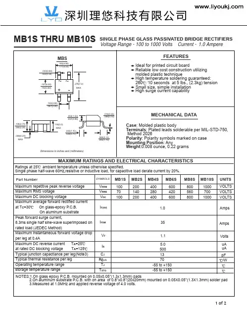
RATINGS AND CHARACTERISTIC CURVES MB1S THRU MB10S
I(AV), AVERAGE FORWARD RECTIFIED CURRENT (A)
0.6
IF, INSTANTANEOUS FORWARD CURRENT (A)
100
Fig. 4 Typical Junction Capacitance
TJ = 25°C f = 1.0MHz
20
Cj, JUNCTION CAPACITANCE (pF)
10
10
10
TA = 25°C Single Half Sine-Wave Pulse Width = 8.3ms (JEDEC Method)
Ideal for printed circuit board Reliable low cost construction utilizing molded plastic technique High temperature soldering guaranteed: 260 /10 seconds at 5 lbs., (2.3kg) tension Small size, simple installation High surge current capability
IFSM
35
Amps
VF IR CJ R JA TJ TSTG
1.1 5.0 500 13 70 -55 to +150 -55 to +150
Volts uA uA pF /W
NOTES:1.On glass epoxy P.C.B. mounted on 0.05x0.05''(1.3x1.3mm) pads 2.On aluminum substrate P.C.B. with on area of 0.8''x0.8''(20x20mm) mounted on 0.05X0.05''(1.3X1.3mm) solder pad 3.Measured at 1.0MHz and applied reverse voltage of 4.0 volts.
10
1 .0 T J= 2 5 C
O
0 .1 20 40 60 80 100 120
PERCENT OF RATED PEAK INVERSE VOLTGE (V)
2 of 2
.008(0.20) MAX
.083(2.12) .043(1.10)
Dimensions in inches and (millimeters)
MAXIMUM RATINGS AND ELECTRICAL CHARACTERISTICS
Ratings at 25 ambient temperature unless otherwise specified. Single phase half-wave 60Hz,resistive or inductive load, for capacitive load derate current by 20%. Part Number Maximum repetitive peak reverse voltage Maximum RMS voltage Maximum DC blocking voltage Maximum average forward rectified current at TC=30 On glass-epoxy P.C.B. On aluminum substrate Peak forward surge current, 8.3ms single half sine-wave superimposed on rated load (JEDEC Method) Maximum instantaneous forward voltage drop per leg at 0.4A Maximum DC reverse current TA=25 at rated DC blocking voltage TA=125 Typical junction capactiance per leg(Note3) Typical thermal resistance per leg Operating temperature range storage temperature range
1.0
Fig. 1 Output Current Derating Curve
10
Fig. 2 Typical Forward Characteristics (per leg)
1.0
0.4
0.1
0.2
0
0
40
80
120
160
0.01 0.2 0.4 0.6 0.8 1.0
TA= 25°C Pulse WidL DATA
Case: Molded plastic body Terminals: Plated leads solderable per MIL-STD-750, Method 2026 Polarity: Polarity symbols marked on case Mounting Position: Any Weight:0.008 ounce, 0.22 grams
SYMBOLS
MB1S 100 70 100
MB2S 200 140 200
MB4S 400 280 400 1.0
MB6S 600 420 600
MB8S 800 560 800
MB10S 1000 700 1000
UNITS VOLTS VOLTS VOLTS Amps
VRRM VRMS VDC IF(AV)
深圳理悠科技有限公司
MB1S THRU MB10S
MBS
.193(4.90) .177(4.50) .033(0.84) .022(0.56)
SINGLE PHASE GLASS PASSIVATED BRIDGE RECTIFIERS Voltage Range - 100 to 1000 Volts Current - 1.0 Ampere FEATURES
TA, AMBIENT TEMPERATURE (°C)
1.2
1.4
1.6
VF, INSTANTANEOUS FORWARD VOLTAGE (V)
I FSM, PEAK FORWARD SURGE CURRENT (A)
Fig. 3 Maximum Peak Forward Surge Current (per leg) 35 30
.157(4.00) .142(3.60)
.276(7.0)
+
MAX
.102(2.60) .087(2.20) .014(0.35) .006(0.15)
.053(1.53) .037(0.95) .106(2.70) .090(2.30) .118(3.0) MAX .043(1.10) .028(0.70)
0
1
1.0
1
10 VR, REVERSE VOLTAGE (V)
100
NUMBER OF CYCLES AT 60 Hz
FIG.5 TYPICAL REVERSE CHRACTERISTICS
INVSTANTANEOUS REVERSE CURRENT (µA)
10 00
100
T J= 125 C
O
MB10S贴片整流桥的具体电性参数,工程师讲解行业规格标准

MB10S是一款小方桥、贴片整流桥堆。
主要应用于小电流领域产品:小功率开关电源,充电器,电源适配器,LED灯整流器等相关电器产品。
MB10S电性参数介绍
整流桥MB10S它的电性参数是:正向电流(Io)为0.5A,反向电压为1000V,正向电压(VF)为1.0V,采用GPP芯片材质,里头有4个芯片,芯片尺寸都是46MIL,它的浪涌电流Ifsm为30A,漏电流(Ir)为5uA、工作温度在-40~+150℃,恢复时间(Trr)达到500ns,里面引线数量有4条。
整流桥MB10S型号它的脚间距为2.5mm,整体长度为4.7mm,高度为2.5mm,厚度为1.1mm,其本体宽度为4.0mm,脚厚度为0.25mm。
台湾进口ASEMI本产品原装正品,质量保证,高稳定性和可靠性,欢迎咨询取样测试。
是您最好的选择!。
MB8S 封装MBS 系列规格书推荐
0
1
1.0
1
10 VR, REVERSE VOLTAGE (V)
100
NUMBER OF CYCLES AT 60 Hz
FIG.5 TYPICAL REVERSE CHRACTERISTICS
INVSTANTANEOUS REVERSE CURRENT (µA)
10 00
100
T J= 125 C
O
.008(0.20) MAX
.083(2.12) .043(1.10)
Dimensions in inches and (millimeters)
MAXIMUM RATINGS AND ELECTRICAL CHARACTERISTICS
Ratings at 25 ambient temperature unless otherwise specified. Single phase half-wave 60Hz,resistive or inductive load, for capacitive load derate current by 20%. Part Number Maximum repetitive peak reverse voltage Maximum RMS voltage Maximum DC blocking voltage Maximum average forward rectified current at TC=30 On glass-epoxy P.C.B. On aluminum substrate Peak forward surge current, 8.3ms single half sine-wave superimposed on rated load (JEDEC Method) Maximum instantaneous forward voltage drop per leg at 0.4A Maximum DC reverse current TA=25 at rated DC blocking voltage TA=125 Typical junction capactiance per leg(Note3) Typical thermal resistance per leg Operating temperature range storage temperature range
MB10S 超小性贴片整流桥内含50mil大芯片

MB10S参数介绍
深圳市强元芯电子有限公司,专注电源领域12年!
供应MB10S贴片整流桥详细参数规格
内部芯片类型:台湾波峰GPP芯片
品牌:ASEMI
最大正向整流电流Io:0.5A
最大反向耐压PRV:1000V
正向压降VFM:1.0V
正向峰值电流:30A
工作温度范围:-40°C to+175°C
最大反向电流:5.0A
封装形式:MBS-4/SOP-4
应用市场:手机充电器、LED灯具等
MBS贴片整流桥相关型号:MB2S、MB4S、MB6S、MB8S、MB10S
强元芯电子是一家技术力量雄厚的公司,12年专注于电源领域的研发经验,可为客户提供全套的技术支持!本公司专业生产整流桥,肖特基,快恢复二极管,为ASEMI大陆地区一级代理商!强元芯在半导体行业有着12年的资质,以诚信经营为宗旨,打造百年诚信企业为方向,本着“客户就是上帝,要满足并超越客户需求”的客户观,快速发展;致力成为中国电子供应链中广大厂商优先选择的战略合作伙伴。
也许我们只是一个小小配件,却是您产品中不可或缺的一份子!
也许我们给你的价格不是最低的,但品质一定是最高的;我们宁可为价格解释一阵子,也不愿为质量道歉一辈子!。
MB2S 封装MBS 系列规格书推荐
TA, AMBIENT TEMPERATURE (°C)
1.2
1.4
1.6
VF, INSTANTANEOUS FORWARD VOLTAGE (V)
I FSM, PEAK FORWARD SURGE CURRENT (A)
Fig. 3 Maximum Peak Forward Surge Current (per leg) 35 30
1.0
Fig. 1 Output Current Derating Curve
10
Fig. 2 Typical Forward Characteristics (per leg)
1.0
0.4
0.1
0.2
0
0
40
80
120
160
0.01 0.2 0.4 0.6 0.8 1.0
TA= 25°C Pulse Width = 300µs
1 of 2
深圳理悠科技有限公司
RATINGS AND CHARACTERISTIC CURVES MB1S THRU MB10S
I(AV), AVERAGE FORWARD RECTIFIED CURRENT (A)
0.6
IF, INSTANTANEOUS FORWARD CURRENT (A)
.157(4.00) .142(3.60)
.276(7.0)
+
MAX
.102(2.60) .087(2.20) .014(0.35) .006(0.15)
.053(1.53) .037(0.95) .106(2.70) .090(2.30) .118(3.0) MAX .043(1.10) .028(0.70)
SYSTIMAX GigaSPEED X10D HGS620 屏蔽式接头终端说明书
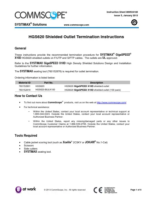
SYSTIMAX ® Solutions Instruction Sheet 860524180Issue 5, January 2013HGS620 Shielded Outlet Termination Instructions© 2013 CommScope, Inc. All rights reservedPage 1 of 6GeneralThese instructions provide the recommended termination procedure for SYSTIMAX ®GigaSPEED ®X10D HGS620 shielded outlets on F/UTP and S/FTP cables. The outlets are UL approved.Refer to the SYSTIMAX GigaSPEED X10D High Density Shielded Solutions Design and Installation Guidelines for further information.The SYSTIMAX seating tool (760152876) is required for outlet termination. Ordering information is listed below:Material ID Part No.Description760152801 HGS620HGS620 GigaSPEED X10D shielded outlet760152819HGS620-BULK100HGS620 GigaSPEED X10D shielded outlet (100 pack)How to Contact Us• To find out more about CommScope ®products, visit us on the web at / •For technical assistance:-Within the United States, contact your local account representative or technical support at 1-800-344-0223. Outside the United States, contact your local account representative or Authorized Business Partner.-Within the United States, report any missing/damaged parts or any other issues to CommScope Customer Claims at 1-866-539-2795. Outside the United States, contact your local account representative or Authorized Business Partner.Tools Required• Cable jacket scoring tool (such as Xcelite ®2CSKY or JOKARI ®No.1-Cat) • Scissors • Side cutters•SYSTIMAX seating tool.860524180Instruction SheetPage 2 of 6Preparation of F/UTP Cable for Termination1.scoring tool that has fine adjustment settings, such as the Xcelite JOKARI No.1-Cat.2. jacket.3. Trim off clear cellophane wrapping.4. Separate the pairs, cut the flute flush with endof jacket and restore pairs to their original positions. 5. Ensure that foil is pressed tight over thejacket and then wrap drain wire around foil close to end of cable. Do not overlap drain wire when wrapping. 6. Arrange pairs in the order below:• Brown • Blue • Orange • GreenPreparation of S/FTP Cable for Termination1.scoring tool that has fine adjustment settings, such as the Xcelite JOKARI No.1-Cat.2.over cable jacket.Brown pair860524180Issue 5, January 2013Page 3 of 61. termination manager with pair colors oriented to the labels on the termination manager.Important:cable or braided shield on S/FTP cable will manager.2. engage and a click is heard.Note: F/UTP cable shown.Score foil shield1” (25mm)Braided shieldDrain wire860524180Instruction SheetPage 4 of 6Seat and Trim Conductors1. Following the label colors (T568B shown),place conductors directly into termination slots. Seat conductors by pulling tight into slots, then trim pairs flush.Seat Termination Manager on Outlet Body1. Carefully align and insert terminationmanager squarely into outlet body.Note : For correct orientation, the Brown label side faces the 3 notches.2. If outlet will be used in a Keystone compatibleopening, insert Keystone clip on outlet before placing it in seating tool and seating termination manager to outlet body.Note: The clip has three tabs that slide into three notches on outlet body.Orange pairGreen pair860524180Issue 5, January 2013Page 5 of 6For F/UTP cable only, trim excess foil.6. If outlet will be used in a faceplate or boxapplication, attach M-series adapter.Note : The M-series adapter is not allowed where grounding is required.Foil860524180Instruction SheetPage 6 of 6Inspection or Repair of TerminationNote: To enable inspection or repair, the termination manager can be released from the outlet body by inserting a small flat blade screwdriver in slot located on either side of outlet and twisting as shown.To release the termination manager, insert a small flat blade screwdriver between the two halves as shown and twist to disengage the latches.A spudger tool can then be used to remove conductors for repair.Installation in Shallow BoxesIt is acceptable to bend the exiting cable up to 90°, as tight as necessary, in any direction. Use care to ensure the cable shield remains inside the termination manager.Slot。
MB2F-MB10F MBF 系列规格书推荐

IF, INSTANTANEOUS FORWARD CURRENT (A)
Fig. 2 Typical Forward Characteristics (per leg) 10
0.8
Al. Substrate PC Board
1.0
0.6
0.4
Glass Epoxy PC Board
0.1
0.2
IFSM, PEAK FORWARD SURGE CURRENT (A)
Fig. 3 Maximum Peak Forward Surge Current (per leg) 35 30
Cj, JUNCTION CAPACITANCE (pF)
100
Fig. 4 Typical Junction Capacitance
TJ = 25°C f = 1.0MHz
20
10
10
TA = 25°C Single Half Sine-Wave Pulse Width =8.3ms (JEDEC Method)
0
1
1.0
10 NUMBER OF CYCLES AT 60 Hz
1
10 VR, REVERSE VOLTAGE (V)
MB2F THRU MB10F
MBF
SINGLE PHASE GLASS PASSIVATED BRIDGE RECTIFIERS Voltage Range - 200 to 1000 Volts Current - 0.5/0.8 Ampere
FEATURES
Glass passivated die construction Low forward voltage drop High current capability High surge current capability Designed for surface mount application Plastic material-UL flammability 94V-0
MB1S-MB10S封装MBS 系列规格书推荐
IFSM
35
Amps
VF IR CJ R JA TJ TSTG
1.1 5.0 500 13 70 -55 to +150 -55 to +150
Volts uA uA pF /W
NOTES:1.On glass epoxy P.C.B. mounted on 0.05x0.05''(1.3x1.3mm) pads 2.On aluminum substrate P.C.B. with on area of 0.8''x0.8''(20x20mm) mounted on 0.05X0.05''(1.3X1.3mm) solder pad 3.Measured at 1.0MHz and applied reverse voltage of 4.0 volts.
1.0
Fig. 1 Output Current Derating Curve
10
Fig. 2 Typical Forward Characteristics (per leg)
1.0
0.4
0.1
0.2
0
ASEMI整流桥MB10S出来的电压是多少,MB10S加多大电容
ASEMI整流桥MB10S出来的电压是多少,MB10S加多⼤电容编辑-ZMB10S参数描述型号:MB10S封装:MBS-4 (SOP-4)特性:⼩⽅桥、贴⽚桥堆电性参数:1A 1000V芯⽚材质:GPP正向电流(Io):1A芯⽚个数:4正向电压(VF):1.0V芯⽚尺⼨:50MIL浪涌电流Ifsm:30A漏电流(Ir):5uA⼯作温度:-55~+150℃引线数量:4ASEMI整流桥MB10S出来的电压是多少?整流电压的输出电压⼤家⼀定很熟悉。
很多⼈会说输出平均值是全波0.9倍,半波0.45倍有效。
但在设计中,我们经常会发现⼀个事实,⽐如半波整流后,输出电压在0.45倍以上,9V交流整流后可能是11-12V。
我之前⼀直很困惑,是不是我记错了倍数的计算?看了很多书,公式当然是正确的,那是怎么回事呢?可能是我们之前在学校学习这个知识点的时候对整流电路太关注了,忽略了脉动⽐的概念,所以很多⼈对这个简单的知识不是很清楚。
其实这是因为整流电路后⾯接了滤波电容。
看模电的知识可以知道,整流后往往加滤波稳压,滤波电路会改变整流输出的脉动⽐,并与负载有关。
因此,最终MB10S整流后得到的电压不仅与整流⽅式有关,还与负载和滤波电容的⼤⼩有关。
RL*C 的值直接影响输出电压的⼤⼩。
因此,MB10S加多⼤电容?滤波电容的选择不是任意的,⽽是需要根据负载情况选择合适的值。
MB10S滤波电路接通后,输出电压平均值约为1.2倍,负载开路为1.414倍。
RC=(3-5)T/2决定电容选择。
其中T表⽰电⽹周期。
电容滤波电路适⽤于⼩负载电流,⽽电感滤波电路适⽤于⼤负载电流。
(电流⼤时R⼩,C难选)可以计算,但⽅法不简单,必须详细给出负载、整流管参数、变压器参数等,没有太⼤的实际意义。
FOSAN富信电子 二极管 MB1S-MB10S-产品规格书
安徽富信半导体科技有限公司ANHUI FOSAN SEMICONDUCTOR TECHNOLOGY CO.,LTD.MB1S-MB10SBridge Rectifier Diode 整流桥■Features 特点Glass passivated chip junction 玻璃钝化结High surge current capability 高浪涌电流能力Reflow Solder Temperature 220℃回流焊温度220度Package 封装:MBS■Maximum Rating 最大额定值(T A =25℃unless otherwise noted 如无特殊说明,温度为25℃)Characteristic 特性参数Symbol 符号MB1S MB2S MB4S MB6S MB8S MB10S Unit 单位Peak Reverse Voltage 反向峰值电压V RRM 1002004006008001000V DC Reverse Voltage 直流反向电压V R(DC)1002004006008001000V RMS Reverse Voltage 反向电压均方根值V R(RMS)70140280420560700V Forward Rectified Current 正向整流电流I F 0.8A Peak Surge Current 峰值浪涌电流I FSM 30A Thermal Resistance J-A 结到环境热阻R θJA 90℃/WJunction and Storage Temperature 结温和储藏温度T J ,T stg150℃,-55to+150℃■Electrical Characteristics 电特性(T A =25℃unless otherwise noted 如无特殊说明,温度为25℃)Characteristic 特性参数Symbol 符号Min 最小值Typ 典型值Max 最大值Unit 单位Condition 条件Forward Voltage 正向电压降V F 1.01.1V I F =0.4A 0.8A Reverse Current (T A =25℃)反向漏电流(T A =125℃)I R 540uA V R =V RRM Diode Capacitance 二极管电容C D13pFV R =4V,f=1MHzANHUI FOSAN SEMICONDUCTOR TECHNOLOGY CO.,LTD.MB1S-MB10S ■Typical Characteristic Curve典型特性曲线Figure1:Forward Current Derating Curve Figure2:Peak Forward Surge CurrentFigure3:Instantaneous Forward Characteristics Figure4:Reverse Leakage CharacteristicsFigure5:Junction Capacitance CharacteristicsANHUI FOSAN SEMICONDUCTOR TECHNOLOGY CO.,LTD.MB1S-MB10S ■Dimension外形封装尺寸。
贴片整流桥的作用是什么?ASEMI贴片整流桥有哪些型号?
对于工程师来说,贴片整流桥的作用很简单,相对于非专业人士就比较难理解了,ASEMI课堂接下来就详细介绍贴片整流桥作用以及它都有哪些型号。
贴片整流桥作用:整流桥是把交流电转变成直流电,是一款可以把交流转变成直流的整流元件,其电路有两种,分别是电相整流电路和三相整流电路,贴片整流桥的作用也是一样的,把交流电变成直流电,我们将分别从正向和反向两个方向为大家讲解:上图所示,是输入电流为正向时,D1,D3工作,整流桥的输出波形,从它的输出波形图中可以看出,在这一方向时刻,整流桥负半轴的电流通过整流桥后都变为正半轴,这是它正向的一个工作电路图。
下图所示,为反向时它的工作电路图:反向工作时,D2和D4工作,整流桥依然可以把负半轴的电流变为正半轴,右图当中是它的波形输出图,贴片整流桥型号封装:MBS封装:MB1S、MB2S、MB4S、MB6S、MB8S、MB10SMBM封装:MB1M、MB2M、MB4M、MB6M、MB8M、MB10MMBF封装:MB1F、MB2F、MB4F、MB6F、MB8F、MB10FHD封装:HD02、HD04、HD06、HD08、HD10ABS封装:ABS2、ABS4、ABS6、ABS8、ABS10DB封装:DB104、DB105、DB106、DB107、DB154、DB155、DB156、DB157、DB204、DB205、DB206、DB207DBS封装:DB104S、DB105S、DB106S、DB107S、DB154S、DB155S、DB156S、DB157S、DB204S、DB205S、DB206S、DB207SASEMI品牌所以产品均通过UL安全认证及SGS环保认证,采用台湾进口晶圆波峰GPP芯片制造而成。
GPP芯片具有良好的散热性,较强的稳定性,可信赖性极佳,采用台湾健鼎一体化测试设备测试,保障每一颗产品出产都99.99%合格。