翻译(非平衡磁控溅射阴极的优化研究)
磁控溅射原理介绍(英文)

Magnetic Field B
+
E
x
x x Bx
-
Main Menu
MIRDC
What is a Magnetron
The most common type of magnetron can be found inside a microwave oven.
This is a magnetron tube.
Control of these highly mobile plasma electrons is the key to all forms of plasma control
Conversion of a neutral atom
into an ion by electron collision
(for ion energies < 1keV).
Ar+
Main Menu
MIRDC
Ionising collisions
Ions and electrons lost from the discharge can be replaced by ionising collisions
⇒ e- + Ar e- + e- + Ar+
in a plasma
0+ e-
e1+
Main Menu
MIRDC
Electron motion in a combined electric & magnetic field
e-
SN E
B ExB
B
x
B
e-
NS
e-
Main Menu
MIRDC
非平衡磁控溅射技术在刀具涂层上的应用
干式切削技术在我国不断推广与发展 , 对刀具涂层的要求
也在不断的提高 , 针对 不同的工作环境 , 一涂 层材 料难 以满 单 足干式切 屑加工对涂层的要求 , 刀具涂层也趋向于纳米层状结
构 和 化 学 组 分 多元 化 等 方 向发 展 , 疑 , 些 薄 膜 技 术 的研 究 无 这
同时用 C作为基体还 可以加人A, , iV r 1Mo T, 和Y等多种元 素来改变涂层 的化学组成 , 从而形成多层复合纳米涂层来调节
的使用性能要求, 涂层设 计 由三部分组成 : 金属c 底层 , 作 保证
涂 层 与 基体 附着 良好 ; CN 成 过 渡 层 , 善 涂 层 的抗 振 性 用 r构 以改
层, 通过优化 它们 的晶格结构 , 来降低涂层 间内应力 , 使之具有
很高 的硬度和耐磨性 ,中部渐进的氮化铬涂层作 为隔热层 ; 通 过抑制从切削区到刀片 的热传导来 降低热冲击 ; 同时还可在外 层镀上低摩擦系数 的M S等减少摩擦力及摩擦热 ,可实现 固 o2
r n e st n t e a h so n t c u e o o t g d — e t d n i o h d e in a d sr t r c a n e y u f i
涂层化学成分 硬度 (咖 m ) k 2
C A1 r N
CI r N I
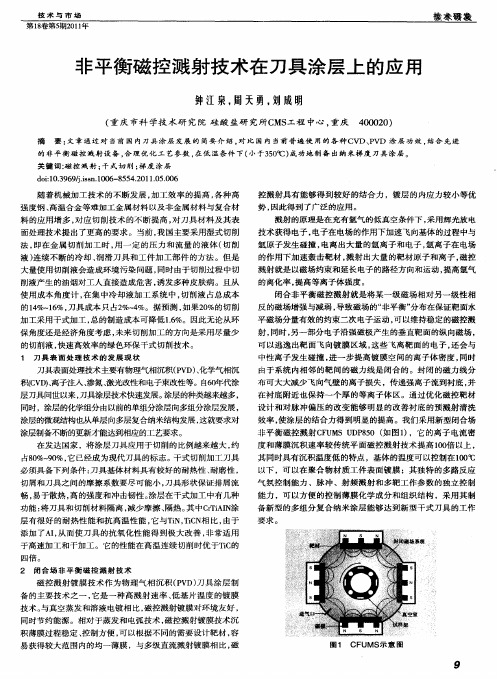
中性离子发生 碰撞 , 一步提 高镀 膜空间 的离 子体 密度 , 进 同时
由于 系统 内相 邻 的靶 间的磁力线是 闭合 的 。封闭 的磁 力线分 布可大大减少飞 向气壁 的离子损失 ,传递强离子流到衬底 , 并 在衬底附 近也 保持一个厚 的等离子体 区 。通过优化磁 控靶 材 设计和对 脉冲偏压 的改 变能够 明显 的改善衬底 的预溅 射清洗 效率 , 使涂层 的结合力得 到明显的提高 。我们采用新型闭合场 非平衡磁 控溅射C U S U P 5 ( 图 1 ,它的离子 电流 密 F M D 80 如 ) 度和薄膜沉积 速率较传统 平面磁控溅射 技术提高 1o 以上 , 0倍
基于ANSYS的(非)平衡磁控溅射镀膜机磁场模拟解读

Y93乏377硕士学位论文基于ANSYS的(非)平衡磁控溅射镀膜机磁场模拟作者:崔著双指导教师:杭凌侠教授申请学位学科:光学工程西安工业大学2006年3月摘要基于ANSYS的(非)平衡磁控溅射镀膜机磁场模拟研究生签字:崔蔫及灵指导教师签字:枯越峡摘要类金刚石薄膜,是近几年发展起来的一种新型薄膜材料。
这种新型材料,由于在力学、电学、化学、光学等方面具有许多独特的性质,已经广泛应用于许多领域。
非平衡磁控溅射是近几年发展起来的新技术,被认为是较有前途的沉积方法。
本课题结合科研项目对非平衡磁控溅射镀膜机的磁场分布进行了研究,论述了非平衡磁控溅射技术的基本理论;介绍了电磁场数值计算国内外发展状况,叙述了有限元计算电磁场的两种解法;得到求解二维线圈静磁场的有限元算法,并用有限元软件ANsYs对二维线圈电磁场分布作了模拟:得到求解三维线圈静磁场的有限元算法,用ANSYs对三维线圈电磁场分布作了模拟;用ANSYS对(非)平衡磁控溅射镀膜机的磁场进行模拟;测试了(非)平衡磁控溅射镀膜机的磁场分布,来验证(非)平衡磁控溅射镀膜机的磁场分布。
用ANsYS对三维跑道线圈、二维永磁体、三维永磁体分别进行了模拟.在一种新型设备的研制中,用ANsYs对它的磁场分布的前期方案进行了模拟;用ANsYs对闭合式电磁铁进行了模拟,并用磁路理论对它进行了分析通过用ANsYs的UIDL和APDL语言对ANSYS进行二次开发,创建了供用户随时调用的宏文件或缩写,既方便了用户,还为优化设计的参数化建模奠定了基础。
尤其在需要大量重复建模的分析中,优势更为明显。
在磁场计算的基础上,利用uIDL和APDL语言,编制了新的查询程序,研究结果表明:(1)对于二维永磁体,模拟时,不用对称线的诺伊曼边界.条件的结果更与实际相符。
(2)平衡磁控溅射圆形靶的磁场在两个磁极内比较均匀,在磁极之外,会急速衰减。
非平衡磁控溅射镀膜机的磁场,调制线圈起到了很好的作用,使磁场均匀范围大为增大。
磁控溅射靶磁场的模拟优化设计

磁控溅射靶磁场的模拟优化设计摘要:本文基于磁控溅射的磁场分布水平和磁场强度在镀膜性能与质量上影响与价值分析,结合磁控靶材的结构及其磁场的计算方法和步骤的探讨,以及利用ANSYS软件对磁控溅射靶磁场的分布及其相关参数作二维的模拟与分析,对影响磁控溅射磁场分布和磁场强度的主要素和作用机制作详细的分析,以为优化磁控溅射靶的设计,达到正常溅射工作对靶材表面磁场分布及大小的要求提供借鉴与参考。
关键词:磁控溅射;靶材;磁场;ANSYS二维模拟;优化设计磁控溅射作为当下最为常见沉积镀膜技术之一,因其薄膜制备牢固、致密的优势,被广泛应用于材料的表面改性和新材料的开发利用过程之中。
但由于磁性靶材刻蚀不均匀等原因的产生,造成磁控溅射靶的磁场分布、磁性强度和靶材利用率难以满足正常溅射技术的实施,从而导致镀膜质量和性能的偏差。
因此就需要通过对磁控溅射靶的结构参数和磁场进行计算,并利用专用的模拟软件对磁场分布进行仿真的模拟,以此才能精准实现从优化磁场分布及磁场强度的靶材设计与改进层面提高溅射镀膜技术发展水平。
1、磁性靶材的结构1.1磁控溅射的实施原理磁控溅射改变了传统溅射方法沉积镀膜速率低、所需工作气压高、放电不易维持的缺点,其利用磁场来实现对电子运动路径进行延长和束缚,从而有效提升了电子的离化率,达到了对电子能量更加充分的利用。
在此过程中,大量的高能量正离子以有效的沉积速率轰击靶材,并在正交磁场的束缚作用下,实现电子能量耗尽后的低温沉积,以带来更加致密、牢固且物理性能良好的溅射薄膜。
1.2磁性靶材的结构及利用率磁控溅射靶材的结构包括溅射区域(可以分为主溅射区和次溅射区)和非溅射区域,其中每一个区域都包含着靶基厚度、靶材刻槽、水平磁通密度、导磁率等的性能参数,而这些性能参数都会对磁场的分布和磁场强度构成影响,从而影响磁性靶的刻蚀度和利用率,导致镀膜的厚度与性能存在差别。
理论上来说,靶材厚度越薄,厚度分布越均匀,其实现磁场分布、磁性强度和靶材利用率水平也就越高,但是靶材的厚度影响着靶材的使用寿命,因此在对磁控溅射靶磁场进行优化的时候,一方面可以通过在靶表面(一般是在非溅射区域)设置一定形状的槽型图案,实现必要的微观糙化,助力靶材表面上正交磁场的产生;另一方面可以将靶材的次溅射区相对于主溅射区减薄,并在次溅射区的边缘与主溅射区之间设置斜坡状的过渡区域,还需在过渡区与主溅射区及次溅射区的拐点位置引入倒角,以此实现靶材厚度适当削弱的同时,提高靶材的磁性寿命,并实现磁性溅射靶材表面磁场分布的均匀性,强化磁性靶材的利用率和溅射性能[1]。
测控技术与仪器类外文翻译、中英文翻译

过滤阴极真空电弧镀膜技术所制得氧化铝薄膜的结构和特性摘要:通过过滤阴极真空电弧镀膜技术制备氧化铝薄膜时,其内部结构、组成、形态、光学和机械性能被详尽的描述,这些都与制备时氧气的流量有关。
薄膜结构、组成、形态和性能都是很重要的,随着氧气流量的增加,薄膜的结构也由非晶体经过一系列变化到单晶体,随着O/Zr原子比率的增加和Z离子由低氧化作用的状态转化为Zr4+再一次形成非晶体。
形成这样的结构是由于其内部结构的变化而引起的,并且影响其形态和机械性能,以致这种非晶体薄膜表面有一些小簇,其光滑程度就像低硬度的多晶体薄膜。
当反射指数和系数相对接近最大值时,在发射率和光学带宽随着O/Zr比增加时,薄膜的组成来决其光学性能而非其密度。
1.说明在大气压力下由于三种不同温度有多种不同靶形态结构,单晶体时低于1170O C,四面体时为1170-2370O C,2370O C为立方体,知道2680O C时形成金属。
Zr有很高的反射指数,大光学带宽间距,和很低的光损失及在0.3-8范围内高透明度,所以被广泛的应用于光学领域。
此外,Zr具有很高的电介质,低泄露量等特点,最有可能代替做电解质的晶体管。
进而,由于Zr很低的传热性,它成为了装置中隔热层的首选。
Z其他的特性如:高硬度、高抗氧性也使其成为机械材料中的热门。
至今为止,已经有很多制备Z的方法,例如反应磁控溅射,离子辅助反应溅射,化学气相沉积等。
薄膜特性的优劣取决于制备过程及其参数。
过滤阴极真空电子弧镀膜技术,在低电压和高电流状态下工作。
通过磁性机械过滤器来防止微粒从阴极发射。
它提供了一种具有很高能量的沉积离子源,远大于相应的热蒸发和磁控溅射。
能有效去处宏观无用微粒,很明显能提高薄膜质量并拓展其应用。
固有的高能量提高薄膜的附着性和密度。
由于能力是离子辅助沉积中最重要的参数,这种制备的方法已经有了一些应用,已经应用于在高热平衡和高SP3状态下碳薄膜的制备,还合成了一些金属氧化物的薄膜。
《闭合场非平衡磁控溅射沉积的CrAlN薄膜组织结构和性能研究》

《闭合场非平衡磁控溅射沉积的CrAlN薄膜组织结构和性能研究》篇一一、引言随着现代材料科学的发展,薄膜材料因其独特的物理和化学性质在众多领域得到了广泛应用。
CrAlN薄膜作为一种具有高硬度、良好的耐磨性和优异的热稳定性的材料,在切削工具、模具制造以及半导体涂层等领域具有巨大的应用潜力。
本文采用闭合场非平衡磁控溅射技术制备CrAlN薄膜,并对其组织结构和性能进行了深入研究。
二、实验方法1. 材料准备实验所使用的靶材为CrAlN陶瓷靶,基底材料为高纯度金属。
在实验前,对基底进行预处理,包括清洗和表面活化处理,以保证薄膜与基底的良好结合。
2. 制备工艺采用闭合场非平衡磁控溅射技术,通过控制溅射功率、气体流量、沉积时间和基底温度等参数,制备不同厚度的CrAlN薄膜。
3. 检测与表征通过X射线衍射(XRD)、扫描电子显微镜(SEM)以及能谱分析(EDS)等手段对薄膜的组织结构进行表征;利用纳米压痕仪测试薄膜的硬度及弹性模量;通过摩擦磨损试验机评估薄膜的耐磨性能。
三、结果与讨论1. 组织结构分析XRD结果表明,CrAlN薄膜具有典型的面心立方结构。
SEM 观察显示,薄膜表面平整,晶粒分布均匀。
EDS分析表明,薄膜中Cr、Al和N元素的分布均匀,符合预期的化学成分比例。
2. 力学性能分析纳米压痕实验结果显示,CrAlN薄膜具有较高的硬度(约XX GPa)和良好的弹性模量(约XX GPa)。
这表明薄膜具有良好的力学性能,适用于高负载应用。
3. 耐磨性能分析摩擦磨损试验表明,CrAlN薄膜具有良好的耐磨性能。
在相同的试验条件下,与未经涂层处理的样品相比,CrAlN薄膜表现出更低的磨损率和更好的抗磨损性能。
这主要归因于其高硬度和良好的化学稳定性。
4. 影响因素分析通过调整溅射功率、气体流量、沉积时间和基底温度等参数,发现这些参数对CrAlN薄膜的组织结构和性能具有显著影响。
适当的参数组合可以得到具有良好组织结构和性能的薄膜。
非平衡磁控溅射沉积MoS2-Ti复合薄膜结构与磨擦摩损性能研究
非平衡磁控溅射沉积MoS2-Ti复合薄膜结构与磨擦摩损性能研究基于非平衡磁控溅射沉积技术,本研究对MoS2-Ti复合薄膜结构及其磨擦摩损性能进行了深入研究。
通过SEM,XRD等微结构表征手段,分析了不同沉积参数对MoS2-Ti复合薄膜结构和成分的影响。
同时,通过磨擦摩损实验,探究了复合薄膜在不同载荷和速度下的磨损行为及其机制。
实验结果表明,在氩气辅助下的非平衡磁控溅射沉积过程中,制备的MoS2-Ti复合薄膜具有较优异的微结构和成分。
随着沉积能量的增大,MoS2-Ti复合薄膜中MoS2纳米颗粒的尺寸和分布均逐渐增大,Ti元素的比例也随之增加。
此外,通过透射电镜(TEM)的分析发现,沉积能量越大,MoS2的层数也会增加。
这些结果表明,喜极而泣,非平衡磁控溅射沉积技术可以有效调控MoS2-Ti复合薄膜的结构和成分,制备出具有良好的摩擦摩损性能的复合材料。
在载荷为1N,滑动速度为10cm/s的条件下,MoS2-Ti复合薄膜与SiO2基板进行摩擦磨损实验。
结果显示,该复合薄膜展现出了优异的抗磨损性能。
其摩擦系数随着摩擦次数的增加而逐渐下降,磨损质量损失也明显降低。
此外,SEM观察表明MoS2-Ti复合薄膜表面有少量的磨痕,而在材料界面处没有明显开裂和脱落现象。
通过摩擦磨损机理的分析,我们发现MoS2-Ti复合薄膜在磨损过程中产生了一层较为稳定的摩擦膜,其不能只通过单一机理进行解释,包含了化学反应、界面反应和物理吸附三种机制。
综上所述,非平衡磁控溅射沉积技术可以制备出具有较好微结构和成分的MoS2-Ti复合薄膜,并展现出良好的摩擦摩损性能。
给予本研究结果,该药物可以广泛应用于摩擦材料领域,具有重大的研究和应用价值。
为了进一步研究MoS2-Ti复合薄膜的性能和机制,我们还进行了失重和电化学测试。
失重实验表明,摩擦过程中的磨粒发生了微小的质量损失,表明MoS2-Ti复合薄膜具有良好的耐磨性能。
电化学测试结果显示,在模拟海水中,MoS2-Ti复合薄膜的腐蚀电流密度较低,腐蚀电位较高,表明该复合薄膜具有良好的耐腐蚀性能。
磁控溅射法和一步电沉积法制备Cu2ZnSnS4薄膜
华中科技大学硕士学位论文摘要随着化石能源的日益减少,能源危机迫使人们不得不寻找可替代的新能源。
新能源中太阳能来源丰富,是最有可能替代传统能源的清洁可再生能源。
目前,常见的薄膜太阳能电池有CdTe、CIGS(CuIn x Ga(1-x)Se2)和CZTS(Cu2ZnSn4),但是Te、In、Ga是稀有元素,价格昂贵;Cd是重金属元素,安全性受到质疑。
而CZTS与CIGS的光学性质和半导体性质相似,且组成元素储量丰富、价格低廉,有望成为替代CIGS 的后备材料。
本文采用磁控溅射法和一步电沉积法制备CZTS薄膜。
磁控溅射法预制膜成膜质量高,成分比例易控制,但高度依赖后期热处理,本文磁控溅射法重点探讨硫化温度和SnS含量对实验结果的影响。
电沉积法成本低廉,操作简便,但电沉积过程要求高,化学成分难控制,且高度依赖后期硫化处理。
因此,前期通过改变溶液pH 值、离子浓度研究电沉积的影响,后期通过调节硫化时间、硫化温度研究硫化过程对薄膜生长的影响。
利用X射线荧光针(XRF)测定前驱体薄膜元素配比、能谱仪(EDS)测定CZTS薄膜成分、X射线衍射仪(XRD)和拉曼图谱(Raman)分析薄膜的结构、场发射扫描电镜(SEM)观测薄膜的表面和截面形貌。
通过讨论分析得出,磁控溅射法中当硫化温度为580℃,SnS的含量为8mg时CZTS薄膜晶粒生长最好。
电沉积法中最佳pH值为 5.7,最佳离子浓度为22mM(CuSO4·5H2O)、22mM(ZnSO4·7H2O)、8mM(SnSO4),经300℃预处理30min 能改善薄膜形貌,硫化过程中最佳硫化时间为60min,最佳硫化温度为580℃,制备的薄膜表面致密,晶粒均匀,薄膜厚度约为2μm,适合用作吸收层。
关键词:薄膜太阳能电池铜锌锡硫磁控溅射法电沉积法硫化处理华中科技大学硕士学位论文AbstractWith the decrease of fossil fuels, the energy crisis forced people to look for alternative energies.Among the new energies, solar energy is inexhaustible and considered to be the most promising clean and renewable energy. At present, there are three common thin-film solar cells, CdTe, CIGS(CuIn x Ga(1-x)Se2) and CZTS(Cu2ZnSn4). However, Te, In and Ga are rare metals which are very expensive; Cd is a heavy metal element which is questioned for the safety. CZTS has similar optical and semiconductive properties with CIGS, and all elements are abundant and non-toxic. So CZTS is expected to become an alternative material to replace CIGS.In this thesis, magnetron sputtering and one-step electrodeposition methods were used to fabricate CZTS films. Magnetron sputtering technique can control the composition of CZT metal layer properly and get high quality film. But this method highly depends on the sulfurization process. In this study, sulfurization temperature and SnS content were investigated. Electrodeposition is low-cost and simple. But it’s difficult to control the composition during deposition, and it extremely relies on the post annealing process. So during the deposition, the influences of pH value and ionic concentrations were studied. And during the annealing process, the effects of sulfurization time and temperature on the morphology of CZTS were investigated. Thin films were characterized by X-ray fluorescence, Energy disperse spectroscopy, X-ray diffraction and Raman spectroscopy. The surface and cross-sectional images of the films were observed by Scanning electron microscopy.Through the discussion and analysis, we found that in the sputtering method, the CZTS films grew best when the sulfurization temperature was 580℃and the SnS content was 8mg. The optimal pH value of the electrodeposition method was 5.7, the best ion concentration was 22mM (CuSO4·5H2O), 22mM (ZnSO4·7H2O) and 8mM (SnSO4).华中科技大学硕士学位论文Preheating the CZT precursor at 300℃for 30min could improve the morphology of the film. The optimum sulfurization time and temperature was 60min, 580℃, respectively. The prepared film was dense with uniform grains and the thickness was about 2μm, which was suitable for being used as absorber layer.Key words:Thin film solar cell CZTS Magnetron sputteringCo-electrodeposition Sulfurization华中科技大学硕士学位论文目录摘要 (I)Abstract (II)1 绪论1.1研究背景与意义 (1)1.2国内外研究概况 (6)1.3论文的主要研究内容 (8)2 CZTS薄膜的制备方法2.1磁控溅射技术 (10)2.2共蒸镀技术 (11)2.3脉冲激光沉积技术 (11)2.4电沉积技术 (12)2.5溶胶-凝胶技术 (12)2.6喷涂热解技术 (13)2.7丝网印刷技术 (13)2.8涂覆技术 (14)2.9溶液技术 (14)2.10本章小结 (15)3 实验内容3.1磁控溅射法 (16)华中科技大学硕士学位论文3.2电沉积法 (18)3.3实验设备 (20)3.4本章小结 (26)4 结果与分析4.1磁控溅射法结果分析 (27)4.2电沉积法结果分析 (33)4.3对比结果分析 (45)4.4本章小结 (47)5 总结与展望5.1全文总结 (48)5.2课题展望 (49)致谢 (51)参考文献 (52)华中科技大学硕士学位论文1 绪论1.1 研究背景与意义能源是人类不可或缺的物质基础,从原始社会发展至今,社会进步伴随着能源的不断革新。
闭合磁场非平衡磁控溅射离子镀离化特性研究
书山有路勤为径,学海无涯苦作舟
闭合磁场非平衡磁控溅射离子镀离化特性研究
应用闭合磁场非平衡磁控溅射离子镀系统,研究了溅射靶电流、偏压和Ar 流量对偏流密度的影响。
结果表明,偏流密度随着偏压和靶电流的升高而增大,但随偏压的提高偏流密度的增加趋势趋于平缓;偏流密度随着Ar 流量的增大而出现峰值。
磁控溅射离子镀(MS
离化率是指被电离的原子占全部溅射原子的百分比,是磁控溅射离子镀
过程中的一个重要指标。
特别是在活性反应离子镀时,离化率直接反映等离子体的活化程度。
溅射原子和反应气体的离化程度对镀层的各种性质,如附着力、硬度、耐热耐蚀性、结晶结构等,都产生直接的影响。
如何提高等离子体的密度或电离度,以降低气体放电的阻抗,从而在相
同的放电功率下获得更大的电流,也就是获得更多的离子轰击靶材和基体,关键在于如何充分的利用电子的能量,使其最大限度地用于电离。
不同离子镀方法因电离和激发方式不同,其离化率也差别较大。
闭合场非平衡磁控溅射离子镀技术是在普通磁控溅射技术基础上发展起来的一种新型磁控溅射镀膜技术,它是对普通磁控溅射技术进行设备改良和工艺完善的产物。
一块磁控靶的N 极对应另一块靶的S 极,即闭合式结构,闭合式结构将靶系统边缘上的磁力线闭合在两块靶之间,构成逃逸电子的闭合阱,等离子体区域被有效限制在真空室中间区域,即基体所在区域,这样一方面,溅射出来的原子和粒子沉积在基片表面形成薄膜,另一方面,等离子体以一定的能量轰击基片,起到离子束辅助沉积的作用,极大地改善了薄膜质量。
因此,不仅具有普通磁控溅射(MS)过程稳定、控制方便和大面积膜厚均匀性的特点,而且克服了基片附近离子密度。
关于磁控溅射基础知识
磁控溅射目前最重要的工业化大面积真空镀膜技术之一其历史发展如下图所示:发展的驱动力分为以下几点:1.降低工艺成本关注靶材利用率,沉积速率,薄膜均匀性,溅射过程稳定性;2.解决工艺难题和满足进一步提高薄膜性能的工艺参数优化由于低能离子轰击在薄膜沉积中的重要作用,主要要求增加溅射原子离化率,能独立控制/调节微观等离子体工艺参数等,以满足实际镀膜中的多种需求。
其中的HIPIMS 高功率脉冲磁控溅射high power impulse magnetron sputtering;MFMS 中频磁控溅射middle frequency magnetron sputtering;CFUBMS闭合场非平衡磁控溅射closed field unbalanced magnetron sputtering;UBMS 非平衡磁控溅射unbalanced magnetron sputtering;IBAMS 离子束辅助磁控溅射ion beam aiding magnetron sputtering;HCM 空心阴极磁控溅射hollow cathode sputtering;ICPMS 感应耦合等离子磁控溅射inductively couple plasma magnetron sputtering;一,磁控溅射工艺原理相对于其他的制备工艺(CVD,PLD,Spray pyrolysis等),磁控溅射是目前制备薄膜最常用的方法之一。
其主要优点如下:1.较低的制备温度(可室温沉积);2.较高的成膜质量,与衬底附着力好;3.可控性好,具有较高的沉积速率;4.可溅射沉积具有不同蒸汽压的合金与化合物;5.成本较低,重复性好,可实现规模化大面积生产。
按照构造的不同,磁控溅射靶可以分为圆柱靶和平面靶;主要原理:应用一定强度的磁场(50~200mT,能显著影响电子运动但不影响离子运动)和电场(负偏压,约几百V),可以将等离子体(主要是电子)约束在靶面附近(形成非均匀等离子体),增加了碰撞几率,提高了离化效率,因而能在较低的工作气压(0.1~10Pa)和电压下就能起弧/维持辉光放电,而且同时减少了电子对基底的轰击,利于实现低温沉积; 另一方面,这种非均匀等离子体也本质上决定了靶面的非均匀刻蚀以及沉积粒子流量(大致表现为薄膜的沉积速率)和能量分布的空间非均匀性,但这可以通过优化磁控靶结构构造,磁场位形强度分布和移动基体等措施,在一定程度上予以弥补和改善或尽量达到所需的参数。
- 1、下载文档前请自行甄别文档内容的完整性,平台不提供额外的编辑、内容补充、找答案等附加服务。
- 2、"仅部分预览"的文档,不可在线预览部分如存在完整性等问题,可反馈申请退款(可完整预览的文档不适用该条件!)。
- 3、如文档侵犯您的权益,请联系客服反馈,我们会尽快为您处理(人工客服工作时间:9:00-18:30)。
Studies on the optimisation of unbalanced magnetron sputtering cathodes AbstractThe optimisation is reported on the design of unbalanced magnetron (UBM) sputtering cathodes. For the study, a planar circular cathode backed by a double-coil electromagnet (compatible for a 100mm diameter target) was developed. The variation of the structure and strength of the magnetic field in front of the target was investigated for different current combinations in the electromagnetic coils, and its effect on the sputtering process was analysed. The observations on the magnetic field geometry revealed some interesting features, such as the balancing point of the fields along the axis (null-point), and the zero axial region over the target surface (Bz=0 ring). The positions of both could be controlled by adjusting the ratio of the electric current in the coils. The magnetic field null-point could be used as a reference for the region of homogeneous film growth. The Bz=0 ring was the location where the glow discharge concentrated (or where the maximum target erosion occurred). The diameter of the ring determined the area covered by the discharge and thus the sputtering e¦ciency. The optimum substrate position can be Þxed according to the position of the null-point and optimisation of sputtering can be achieved by adjusting the diameter of the Bz=0 ring. The results of this study should be helpful in the designing of an ideal UBM using permanent magnets as well as electromagnets.1. IntroductionThe unbalanced magnetron (UBM) has been the focus of interest for the PVDcommunity for over a decade [1]. While the conventional magnetron sputtering has already made its impact on the thin-film coating industry, the” unbalanced” version proves more advantageous because it combines high deposition rates and low-energy ion bombardment at the substrate. The ion bombardment is achieved by modifying the conventional magnetron (CM) with an additional magnetic field, which deviates the trajectories of secondary electrons from the glow discharge region concentrated near the target, towards the substrate. This would create an ionised region near the substrate and hence causes ion bombardment on the growing film, thereby modifying the properties of the coating [1Ð4].The first ever detailed study of the UBM, is due to Window and Savvides [5]. They analysed dfferent modes of unbalancing the magnetron using permanent magnets and electromagnets, and proved that a magnetic field which converges towards the substrate (Type II, as they designated) gives the desired unbalancing effect. This field distribution was found to maintain considerable ion bombardment over the substrate at low energies, with a high ratio of ion-to-deposited atom.Subsequently, a host of cathode designs appeared in different sizes and shapes, most of them custom-built for laboratory research [1Ð4]. Twin- and multi-cathode configurations were developed in due course, to coat industrial components and a few of such coating systems have appeared in the commercial market also. An excellent review in this regard can be found in Ref. [1].Despite these developments, the understanding about the effects of unbalancing the magnetron on the properties of the Þlms grown, is far from complete. The optimisation studies and the characterisation of the UBM cathodes are rarely reported [6, 7]. Some factors yet remain uninvestigated, like the change in the structure and strength of the magnetic field during unbalancing, and the positioning of the substrates in the unbalancedÞeld, which are crucial in practical considerations. This paper presents preliminary attempts done to have a more complete understanding of the UBM process, namely the effciency optimisation of the cathode.For the study, we designed and fabricated a planar circular magnetron, driven by a double-coil electromagnet. The electromagnet version of the UBM has an advantage that it facilitates the manipulation of the field distribution through the adjustment of currents in the respective coils [4]. A systematic study on the design of the UBM, the principal features of the unbalanced magnetic field and their impact on the optimisation of the sputtering process are discussed in this paper.2. Design of the magnetronThe electromagnet-driven sputtering cathode poses several practical constraints in designing [1, 4]. Electromagnets are normally bulky and heavy, and the coils give rise to outgassing problems inside the vacuum chamber. Therefore, mounting of the magnet outside the chamber is advisable. At the same time, the poles should be as close as possible to the target, to utilise the magnetic field effciently to the maximum extent. The magnet should be electrically isolated from the cathode, to ensure operational safety.Moreover, water flow is to be incorporated for the cooling of the cathode. The present magnetron cathode has been developed considering all these constraints.A schematic of the cathode assembly is shown in Fig. The cathode is made in the form of a flange (200 mm dia,6 mm thick copper disc) which incorporates a target holder (120 mm dia, 6mm thick copper disc). Both are brazed concentrically after machining water channel on the joining faces. The water feeders (6 mm dia copper tubes) are brazed onto the backside of the flange.The electromagnet is made with planar circular pole faces, so that a cylindrically symmetric magnetic field is created in front of the target. It hasa central pole (20 mm dia cylinder) and an annular outer pole (100 mm ID,120 mm OD), both 130 mm long, connected by a backplate. The yoke is fabricated out of a single soft-iron piece, avoiding joints to minimise field losses. Insulated copper wire (18 SWG) is wound on respective poles, to make inner and outer coils. The inner coil has 1880 turns and the outer coil, 1000. As the coils can carry the operating currents (up to 3 A) without overheating, no special cooling is provided for the magnet.The electromagnet is placed concentrically behind the water-cooled cathode. The magnet is isolated from the cathode using PTFE insulation. The assembly is mounted in sputter-down configuration on the top plate of the chamber, with the necessary vacuum seals and electrical isolation.3. CharacterisationA knowledge of the magnitude and direction of the magnetic field near the cathode is essential while optimising the parameters for sputtering. However, this is not easy as the field varies continuously from point to point.The reported data on the magnetic field geometry of the magnetrons are based on computer simulation curve fi tting techniques [6, 8Ð10]. In the present case we made use of the compass needle, the classical tool for plotting the magnetic field, and plotted the actual field. The field line plots corresponding to the inner and outer coils are shown in Fig. 2a and b, respectively. Any variation in the coil currents results in a change in the field strength however, without altering the general nature of the field distribution. The plot for the combination field of both the coils is shown in Fig. 3. When both the coils are powered with opposite polarity, most of the field lines emanating from the central pole converge to the outer pole.A tunnel of field lines is formed in between the circular poles. As the outer pole becomes stronger, additional field lines from the periphery bend over the tunnelled region and run downwards parallel to the axis forming a typical Type II unbalanced field [5]. This field structure is observed to be highly sensitive to the ratio of currents in the coils which is in conformity with the earlier observations [6].The field strength measurements are done with the help of a Gaussmeter using transverse-type Hall probe. This seems more straightforward than the computational methods [8, 9], and of great help in the real-time optimization of the magnetron. As the field is cylindrically symmetrical, the radial and axial components (Br and Bz, respectively) would suffice to give necessary information about it. The vector sum of these components at any point gives the total B at that point.The field values have been measured in front of the target. When the inner coil alone is operating, the axial field maximum (Bz on the magnet axis) at the target surface is 350Ð680G, and the radial field maximum (Br along the target surface) is 150Ð270G for 1Ð3A currents respectively (Fig. 4a and b). The outer coil, due to its larger diameter, contributes only a fraction of these values (20Ð80G in the centralregion, for 1Ð3A currents).This additional field, however, is sufficient to create the unbalance.The field strength distribution in front of the magnet (total B) is determined graphically, after measuring the Br and the Bz values at each discrete point and taking their vector sum. The total field at 1.5A current in each coil, is represented as an isogram in Fig. 5.It is known that the discharge characteristics are controlled by the Br component in front of the target surface.The glow discharge will concentrate in the region where the Br components orient parallel to the target, in other words, where the Bz components become zero [8]. It is the locus of Bz =0 points which determine the erosion track. Therefore, an attempt has been made to study the variation in the Bz components along the target surface and the effect of outer coil current on it. The plot for fixed inner coil current of 1.5A at different outer coil currents is shown in Fig. 6. It can be observed that the Bz=0 ring (the radius of which is indicated by the cross-over point on the x-axis) shrinks as the outer field becomes stronger.4. Discussionhe studies on the field distribution gives an insight into the creation of a Type II unbalanced field in front of the target. It is to be noted that a null-point forms on the magnet axis where the field lines meet and balance (Fig.3). The distance of this point from the magnet plane changes according to the ratio of currents in the coils. The null-point appears to be an interesting feature, which was not analysed in the earlier UBM studies. The Þeld structure above and below this point is totally di¤erent, and hence the same will be the case with the ion (or electron) bombardment during sputtering.A comparison of Figs. 3 and 5 will give a clear idea about the magnitude and direction of the unbalanced field. The value of totalB decreases along the axis and becomes zero at the null-point. The zero-B region at the null-point spreads across (at about 5 cm dia) as a cup shaped surface, parallel to the target plane. The field does increase thereafter, but the increment is not substantial. The total B remains in between 10 and 20G (which is the field reported for most of the UBM cathodes [11]) to a distance of several centimeters beyond null-point. The field in the region below the null-point is almost constant in magnitude and direction throughout a large volume, as evident from Fig. 5. This ensures a uniform ion bombardment and a homogeneous film growth, even on a considerably large,three-dimensional substrate.These studies indicate the methodology of optimising the UBM sputtering, for an ideal combination of high deposition rate and ion bombardment on the substrate.4.1. Optimisation of the substrate positionThe characteristics of the unbalanced field (Figs. 3 and 5) imply that the substrate positioning is very crucial in UBM sputtering. To avail the true advantage of the unbalancing (i.e. to have su¦cient ion bombardment), the substrate should be kept below the null-point. The immediate vicinity of the null-point is not advisable because of low values of Þe ld strength (Fig. 5). Keeping substrate far below, however, will result in the reduction of deposition rate. The optimum position will be in between 1 and 2 cm below the null-point.4.2. Optimisation of the sputteringSputtering experiments done (with OFHC copper target in argon) at various combinations of the magnetic fields, showed that the sputtering parameters are strong functions of the field structure in front of the target. The ratio of the inner and the outer coil currents affects the field line shape of the tunnelled region, which in turn, decides the area of the target covered by the glow discharge. Most effcient sputtering (for a given magnetic field strength and pressure) occurs when the glow discharge covers the maximum target area. This condition is satis fied only when the Bz=0 ring takes a position where the circular area inner to it equals the annular area outside. In the case of a 100mm target, this position corresponds to the Bz=0 ring diameter of 70mm. Circular planar UBMs of any size can be optimised in a similar way, by manipulating the currents in the magnetic coils.The optimisation is tested in actual sputtering conditions by observing the discharge current, which is an indication of efficiency of ionisation at any given voltage. Fig. 7 shows the variation of the discharge current as a function of outer coil current, for different inner coil currents at a fixed discharge voltage of 500V. For a given inner field, the discharge current goes to a maximum at a particular value of outer field. The peak values of discharge current depict the case of optimum sputtering with highest sputtering rate, obtainable at the magnetic field and pressure values. The field ratios at each peak correspond to a Bz=0 ring of diameter 70mm, confirming the geometrical condition for glow discharge coverage.4.3. The erosion zoneObservations on the erosion zone at the optimised conditions is done by sputtering an OFHC target in argon at 0.1Pa. The erosion zone practically covered the whole target area. The region immediate to the Bz=0 ring eroded more, leaving a broad X-shaped groove. After eroding the target to a few millimetres depth, the target utilisation is calculated. The volumetric utilisation is found to be 42%. This is obviously a better value when compared with the utilisation in the range 25-30% reported for planar circular magnetron cathodes [1, 12].5. ConclusionA systematic analysis of the magnetic field in front of a planar circular magnetron cathode is carried out in order to have an optimised "unbalanced" sputtering. An unbalanced magnetron cathode based on double-coil electromagnet has been designed and fabricated for the purpose. The variations in the structure and strength of the field are recorded at different combinations of currents in the coils of the magnet, and their effect on the sputtering is observed. The investigation indicated the methodology of unbalancing and optimising the sputtering cathode design.A typical Type II unbalanced field can be obtained by giving additional field at the periphery of the cathode. A “null-point” occurs on the axis where the fields due to the coils balance. This point can be taken as a reference to decide the substrate position, so that the real unbalance effect can be availed.The glow discharge will be concentrated on the target surface along the circle where the Br components fall parallel (or where the Bz components go to zero). The optimum sputtering occurs when this ring occupies such a position that the glow discharge covers the maximum area on the target. This condition can be achieved by carefully matching the ratio of the magnetic fields and identified practically by observing the Bz=0 position. The optimized Bz=0 ring position will give the largest discharge current during sputtering, for given values of cathode voltage, magnetic field strength and pressure. This optimised condition also gives the highest sputtering rate and the broadest erosion zone. This study shows the possibility of optimising a circular planar UBM cathode during the design stage itself by observing the Bz=0 ring diameter, without going for actual sputtering. The procedure of optimisation (i.e.finding the null-point and identifying the Bz=0 ring) is rather simple that it can be done using a Hall probe. The same methodology is as well applicable to UBM based on permanent magnet. The field structure manipulation in this case can be done through the adjustment of the magnet position or by employing appropriately designed pole pieces.AcknowledgementsThe financial aid for the work under the Indo-US(ONR Grant No. N00014-95-/-1282) fund is gratefully acknowledged. The authors thank the other colleagues in the laboratory for their helpful discussions.References[1] Rohde SL. In: Francombe MH, Vossen JL, editors. Physics ofthin Þlms New York: Academic Press. 1994;18.[2] Window B. Surf Coat Technol 1995;71:93.[3] Mohan Rao G, Mohan S. Ionics 1995;12:53.[4] Sproul WD. Surf Coat Technol 1991;49:284.[5] Window B, Savvides N. J Vac Sci Technol 1986;A4:196.[6] Kadlec S, Musil J. J Vac Sci Technol 1995;A13:389.[7] Muralidhar GK, Musil J, Kadlec S. Rev Sci Instr 1995;66:4961.[8] Perlov CM, Brauer JR. IEEE Trans Magn 1986;MAG-22:831.[9] Wong MS, Sproul WD, Rohde SL. Surf Coat Technol 1991;49:121.[10] Murphy MJ, Cameron DC, Karim MZ, Hashmi MSJ. Surf CoatTechnol 1993;57:1.[11] Musil J, Kadlec S, Munz WD. J Vac Sci Technol 1991;A9:1171.[12] Schiller S, Heisig U, Goedicke K. Thin Solid Films 1977;40:327.非平衡磁控溅射阴极的优化研究摘要报道了非平衡磁控溅射阴极的运转设计。