LED可变信息标志(情报板)技术及使用手册V2.2L
基于Niosll的LED可变情报板控制系统

圈 1
LD E可变情报板系统的核心是控制器 ,E 可变情报板 控制器 接收 LD 主控计算机传来 的指令 ,调 用预 先存放在控制器 中的各种数据信息 ,
按照要 求把接收的指令处理成显示屏需要的点阵数据 布到显 示屏 发 上 广泛采用的是单片机 + S 、 D P 工控机 或嵌 入式工控机 以及单 片机 加 大规模 可编程器件的构成方式。 基于Nol i l s软核的LD 变情报板控制系统与一般系统主要的差别 E可 是选用基于 N s 微处理器作为控制器的处理器 , it ot 并具有 以太 网、 口 串 和 UB S 通信等多种数据传输方式。以太网的通信方式可以方便 地进行
缩短 . 加快了产品进入 市场的时间 . 减少了开发的成 本。 O C是 PD SP L 和 A I技术融合的结果 . S C 集成 了硬核或者软核C U S 、 P D P 存储器 、 外 围l O及可编程逻辑 的 S P O C芯片 . 在应用 的灵活性 和价格上有极大的 优势。基于Nol i l s 的这种设计通过其 U R 可 以连接 多个 串 1和U 8 AT 2 S 接 I. : 还可以使用其以太 网接I进行 网络通信 的设计 , 1 : 1 这就使得信息的
技术 前的 L E D可变情 板控制技术 报 来说仍有一定的局限性 LD E 可壹情报撮系境的控制技术成本较高 数据 显 量 越 越 太 控制越 越蔓杂
法
汪日 i月 勺 目 ± 墨表现在 下几十方面
LD E 日鸾情报板 统 控制 挂 也迅 速 提升
研发时间长. 升级 是很便利. 一般没有连接到 太阿
集群控 制,提供远程升级和 F G P A配置
整个系统控制 的过程为: 监控 中心计算机通过网络或串 I向控制 : 1 器发送通信指令 。 控制器接收计算机的指令 。 并按照通信信号 , 输出至 LD像 E
5204.02悬臂门架式LED可变道路情报板(信息显示设备安装

台班 台班
8009025
汽车式起重机 提升量t 5以内
台班
470.10 949.74 637.22
8009029
汽车式起重机 提升量t 20以内
台班
8021014
光纤熔接机
台班
8021016
光时域反射仪
台班
8099001
小型机具使用费
元
1208.73
109.82 630.43 1.00
521.02 0.000 0.440 206.85 0.440
1套
、线缆连接、电气调
合计量 总价
2306.28 2306.28
15.53 13.23 2.30
521.02 206.85
0.00 235.77
0.00 0.00 0.00 78.40
2842.82 2842.82 255.85 216.91 298.40
3315.59 3613.99
1
单位
单价
元
工日 106.28
单位量
合计量
定 额 定额单价 数 量
2306.28
21.700 2306.28 21.700
元
kg
7.35
元
1.00
15.53 1.800 13.23 2.300 2.30
1.800 2.300
三
机械使用费
元
8007003
载货汽车 载货量t 4以 内
8007024
平板拖车组 载货量t 20以内
0.00 0.000 0.370 235.77 0.370
0.00 0.000
0.00 0.00 78.400 78.40
0.000 0.000 78.400
AlInGaP II LED产品说明书

Features• Characterized by radiometric intensity • High optical power output • Extremely long useful life • Low power consumption• Well de ned spatial radiation patterns • 639 nm PEAK red color • 30° viewing angle• High operating temperature: T jLED = +130°C • Superior resistance to moisture • Suitable for outdoor useApplications• Photo sensor stimulus • Infrared emitter replacement • Solid state optical mouse sensors • Surface imaging sensors• Optical position and motion sensors • Human interface devices• Computer printer dot quality control • Battery powered systemsBene ts• Radiometric LED characterization decreases system variability• Improved system reliability • Visual styling• Visible color for improved application safety • On/o indication• Suitable for a variety of sensor-based applicationsDescriptionRadiometrically Tested Precision Optical Performance AlInGaP II (aluminum indium gallium phosphide) LEDs o er increased sensor-based application design exibility. High-resolution radiometric intensity bins (mW/sr) enable customers to precisely match LED lamp performance with sensor functionality.Visible LEDs o er new styling alternatives — light can be leveraged to develop more attractive products. In com-parison to invisible infrared sources, safety concerns are signi cantly improved by the human autonomic pupil response and re exive movement away from bright light. Visible LEDs further indidcate system on/o status.The AlInGaP II technology provides extremely stable light output over very long periods of time, with low power consumption.These lamps are made with an advanced optical grade epoxy system o ering superior high temperature and moisture resistance performance in outdoor systems. The epoxy contains both uv-a and uv-b inhibitors to reduce the e ects of long term exposure to direct sunlight.Please contact your Avago Technologies Representative for more information and design for manufacture advice. Application Brief I-024 Pulsed Operating Ranges for AlInGaP LEDs vs. Projected Long Term Light Output Performance and other application information is available at: /go/led_lamps.HLMP-ED80Radiometrically Tested AlInGaP II LED Lamps for Sensor-Based ApplicationsData SheetMinimum Radiometric Intensity Maximum Forward Voltage Part Number (mW/Sr) at 20 mA (V) at 20 mA HLMP-ED80-K0T00 7.2 2.6HLMP-ED80-K00007.22.4Device Selection GuidePackage DimensionsNOTE:ALL DIMENSIONS ARE IN mm (INCHES).(0.039)CATHODEFLATPart Numbering SystemH L M P-x x x x-x x x x xMechanical Option00: BulkV F Bin Selections0: Maximum V F 2.4 VT: Maximum V F 2.6 VMaximum Intensity Bin0: No maximum Iv bin limitMinimum Intensity BinRefer to device selection guideColorD: 630 nm redPackageE: T-1 3/4 (5 mm) round lamp Note: Please refer to AB 5337 for complete information on part numbering system.Absolute Maximum Ratings at T A = 25°CDC Forward Current [1,2,3].....................................................................................................50 mA Peak Pulsed Forward Current [2,3].......................................................................................100 mA Average Forward Current .......................................................................................................30 mA Reverse Voltage (I R = 100 µA) .........................................................................................................5 V LED Junction Temperature ........................................................................................................130°C Operating Temperature .........................................................................................–40°C to +100°C Storage Temperature ..............................................................................................–40°C to +100°C Notes:1. Derate linearly as shown in Figure 4.2. For long term performance with minimal light output degradation, drive currents between10 mA and 30 mA are recommended. For more information on recommended drive condi-tions, please refer to HP Application Brief I-024 (5966-3087E).3. Please contact your Avago sales representative about operating currents below 10 mA.Electrical/Optical Characteristics at T A = 25°CParameterSymbolMin.Typ.Max.UnitsTest ConditionsForward Voltage ED80-xx0xx V F 2.00 2.40 V I F = 20 mAED80-xxTxx 2.35 2.60Reverse Voltage V R 5 20 V I R = 100 µAPeak Wavelength λPEAK 639 nm Peak of Wavelength of SpectralDistribution at I F = 20 mA Dominant Wavelength [1] λd 630 nmSpectral Halfwidth ∆λ1/2 17 nm Wavelength Width at Spectral Distribution 1/2 Power Point atI F = 20 mASpeed of Response τs 20 ns Exponential Time Constant, e -t/τs Capacitance C 40 pF V F = 0, f = 1 MHzThermal Resistance R ΘJ-PIN240 °C/W LED Junction-to-Cathode Lead Luminous E cacy [5] ηv155 lm/W Emitted Luminous Power/EmittedRadiant Power at I F = 20 mAViewing Angle [2] 2 θ1/2 30 Deg.Radiometric Intensity [3,4]I e7.2350.50mW/srEmitted Radiant Power at I F = 20 mANotes:1. Dominant wavelength, l d , is derived from the CIE Chromaticity Diagram referenced to Illuminant E.2. θ1/2 is the o -axis angle where the luminous intensity is one half the on-axis intensity.3. The radiometric intensity is measured on the mechanical axis of the lamp package.4. The optical axis is closely aligned with the package mechanical axis.5. The luminous intensity, I v , in candelas, may be found from the equation I v = I e ηv , where I e is the radiometric intensity in watts per steradian and ηv is the luminous e cacy in lumens/watt.6. For option -xxTxx, max. forward votage (Vf) is 2.6 V. Refer to Vf bin table.Figure 1. Relative Intensity vs. Peak Wavelength.Figure 2a. Forward Current vs. Forward Voltage for Option -xx0xx.WAVELENGTH – nmR E L A T I V E I N T E N S I T YC U R R E N T – m A1.00V F – FORWARD VOLTAGE – V2.51004030 1.5 2.0603.0102050RED708090Figure 2b. Forward Current vs. Forward Voltage for Option -xxTxx.Figure 3. Relative Luminous Intensity vs. Forward Current.Figure 4. Maximum Forward Current vs. Ambient Temperature. Derating Based on T JMAX = 130°C.Figure 5. Representative Spatial Radiation Pattern for 30° Viewing Angle Lamps.Radiometric Intensity Bin Limits (mW/sr at 20 mA)Bin IDMin.Max.K 8.5 10.2L 10.2 12.2M 12.2 14.7N 14.7 17.6P 17.6 21.2Q 21.2 25.4R 25.4 30.5S 30.5 36.5T 36.543.9Notes:1. Tolerance for each bin will be ± 15%.2. Bin categories are established for classi ca-tion of products. Products may not be avail-able in all bin categories.3. VF bin table only available for those num-ber with options -xxTxx.Vf Bin Table [3]Bin IDMin.Max.VA2.0 2.2VB 2.2 2.4VC2.42.6Tolerance for each bin limit is ±0.05 V.F O R W A R D C U R R E N T00FORWARD VOLTAGE – V2.55040301.52.03.010201.00.5R E L A T I V E R A D I O M E T R I C I N T E N S I T Y (N O R M A L I Z E D A T 20 m A )00I F – DC FORWARD CURRENT – mA 402.01.51.00.520502.51030I F – F O R W A R D C U R R E N T – m AT A – AMBIENT TEMPERATURE – CN O R M A L I Z E D R A D I O M E T R I C I N T E NS I T YANGULAR DISPLACEMENT – DEGREES0.1110-40-2020406080100T J - JUNCTION TEMPERATURE - ˚CR E L A T I V E L I G H T O U T P U T (N O R M A L I Z E D A T T J = 25˚CFigure 6. Relative Light Output vs Junction TemperaturePrecautions:Lead Forming:•The leads of an LED lamp may be preformed or cut to length prior to insertion and soldering on PC board.•For better control, it is recommended to use proper tool to precisely form and cut the leads to applicable length rather than doing it manually.•If manual lead cutting is necessary, cut the leads after the soldering process. The solder connection forms a mechanical ground which prevents mechanical stress due to lead cutting from traveling into LED package.This is highly recommended for hand solder operation, as the excess lead length also acts as small heat sink. Soldering and Handling:•Care must be taken during PCB assembly and soldering process to prevent damage to the LED component. •LED component may be e ectively hand soldered to PCB. However, it is only recommended under unavoid-able circumstances such as rework. The closest manual soldering distance of the soldering heat source (sol-dering iron’s tip) to the body is 1.59mm. Soldering the LED using soldering iron tip closer than 1.59mm might damage the LED.Note:1. PCB with di erent size and design (component density) will havedi erent heat mass (heat capacity). This might cause a change in temperature experienced by the board if same wave soldering setting is used. So, it is recommended to re-calibrate the soldering pro le again before loading a new type of PCB.Avago Technologies LED con gurationNote: Electrical connection between bottom surface of LED die andthe lead frame is achieved through conductive paste.•ESD precaution must be properly applied on the sol-dering station and personnel to prevent ESD damageto the LED component that is ESD sensitive. Do refer toAvago application note AN 1142 for details. The solder-ing iron used should have grounded tip to ensure elec-trostatic charge is properly grounded.•Recommended soldering condition:Wave Soldering [1, 2]Manual Solder DippingPre-heat temperature105 °C Max.-Preheat time60 sec Max-Peak temperature250 °C Max.260 °C Max.Dwell time 3 sec Max. 5 sec Max Note:1. Above conditions refers to measurement with thermocouplemounted at the bottom of PCB.2. It is recommended to use only bottom preheaters in order to reducethermal stress experienced by LED.•Wave soldering parameters must be set and main-tained according to the recommended temperature and dwell time. Customer is advised to perform daily check on the soldering pro le to ensure that it is always conforming to recommended soldering conditions.•Any alignment xture that is being applied during wave soldering should be loosely tted and should not apply weight or force on LED. Non metal material is rec-ommended as it will absorb less heat during wave sol-dering process.•At elevated temperature, LED is more susceptible to mechanical stress. Therefore, PCB must allowed to cool down to room temperature prior to handling, which in-cludes removal of alignment xture or pallet.•If PCB board contains both through hole (TH) LED and other surface mount components, it is recommended that surface mount components be soldered on the top side of the PCB. If surface mount need to be on the bottom side, these components should be soldered using re ow soldering prior to insertion the TH LED.•Recommended PC board plated through holes (PTH) size for LED component leads.LED componentlead size DiagonalPlated throughhole diameter0.45 x 0.45 mm(0.018x 0.018 inch)0.636 mm(0.025 inch)0.98 to 1.08 mm(0.039 to 0.043 inch)0.50 x 0.50 mm(0.020x 0.020 inch)0.707 mm(0.028 inch)1.05 to 1.15 mm(0.041 to 0.045 inch)•Over-sizing the PTH can lead to twisted LED after clinch-ing. On the other hand under sizing the PTH can cause di culty inserting the TH LED.Refer to Application Note 5334 for more information about soldering and handling of high brightness TH LED lamps.AlInGaP DeviceExample of Wave Soldering Temperature Pro le for TH LEDAmmo Packs DrawingALL DIMENSIONS IN MILLIMETERS (INCHES).NOTE:THE AMMO-PACKS DRAWING IS APPLICABLE FOR PACKAGING OPTION -DD &-ZZ AND REGARDLESS OF STANDOFF OR NON-STANDOFF.4025020015010050TIME (MINUTES)Recommended solder:Sn63(Leaded solder alloy)SAC305(Lead free solder alloy)Flux:Rosin fluxSolder bath temperature:245°C±5°C (maximum peak temperature =250°C)Dwell time:1.5sec -3.0sec (maximum =3sec)Note:Allow for board to be sufficiently cooled to room temperature before exerting T E M P E R A T U R E (°C )10mechanical force.Packaging Box for Ammo PacksPackaging Label(i) Avago Mother Label: (Available on packaging box of ammo pack and shipping box)FROM LEFT ADHESIVE FACING NOTE:THE DIMENSION FOR AMMO PACK IS APPLICABLE FOR THE DEVICE WITH STANDOFF AND WITHOUT STANDOFF.ONFor product information and a complete list of distributors, please go to our website: Avago, Avago Technologies, and the A logo are trademarks of Avago Technologies in the United States and other countries.Data subject to change. Copyright © 2005-2009 Avago Technologies. All rights reserved. Obsoletes 5989-4366EN AV02-1523EN - January 20, 2009DISCLAIMER: AVAGO’S PRODUCTS AND SOFTWARE ARE NOT SPECIFICALLY DESIGNED, MANUFACTURED OR A UTHORIZED F OR S ALE A S P ARTS, C OMPONENTS O R A SSEMBLIES F OR T HE P LANNING, C ONSTRUCTION, MAINTENANCE O R D IRECT O PERATION O F A N UCLEAR F ACILITY O R F OR U SE I N M EDICAL D EVICES O R A PPLI-CATIONS. CUSTOMER IS SOLELY RESPONSIBLE, AND WAIVES ALL RIGHTS TO MAKE CLAIMS AGAINST AVAGO OR ITS SUPPLIERS, FOR ALL LOSS, DAMAGE, EXPENSE OR LIABILITY IN CONNECTION WITH SUCH USE.Acronyms and De nition:BIN:(i) Color bin only or VF bin only(Applicable for part number with color bins but withoutVF bin OR part number with VF bins and no color bin)OR(ii) Color bin incorporated with VF Bin(Applicable for part number that have both color bin and VF bin)(ii) Avago Baby Label (Only available on bulk packaging)Example:(i) Color bin only or VF bin only BIN: 2 (represent color bin 2 only) BIN: VB (represent VF bin “VB” only)(ii) Color bin incorporate with VF Bin VB: VF bin “VB”2: Color bin 2 only。
12通道LED驱动器评估板指南说明书
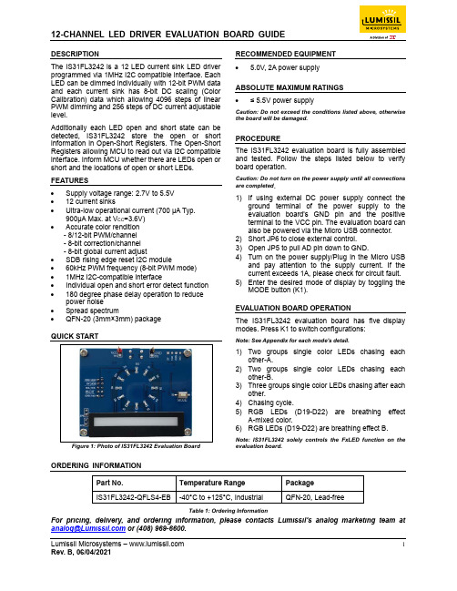
DESCRIPTIONThe IS31FL3242 is a 12 LED current sink LED driver programmed via 1MHz I2C compatible interface. Each LED can be dimmed individually with 12-bit PWM data and each current sink has 8-bit DC scaling (Color Calibration) data which allowing 4096 steps of linear PWM dimming and 256 steps of DC current adjustable level.Additionally each LED open and short state can bedetected, IS31FL3242 store the open orshortinformation in Open-Short Registers. The Open-Short Registers allowing MCU to read out via I2C compatible interface. Inform MCU whether there are LEDs open or short and the locations of open or short LEDs. FEATURES∙Supply voltage range: 2.7V to 5.5V∙12 current sinks∙Ultra-low operational current (700 µA Typ.900µA Max. at V CC=3.6V)∙Accurate color rendition- 8/12-bit PWM/channel- 8-bit correction/channel- 8-bit global current adjust∙SDB rising edge reset I2C module∙60kHz PWM frequency (8-bit PWM mode)∙1MHz I2C-compatible interface∙Individual open and short error detect function∙180 degree phase delay operation to reduce power noise∙Spread spectrum∙QFN-20 (3mm×3mm) packageQUICK STARTFigure 1: Photo of IS31FL3242 Evaluation Board RECOMMENDED EQUIPMENT∙ 5.0V, 2A power supplyABSOLUTE MAXIMUM RATINGS∙≤ 5.5V power supplyCaution: Do not exceed the conditions listed above, otherwise the board will be damaged.PROCEDUREThe IS31FL3242 evaluation board is fully assembled and tested. Follow the steps listed below to verify board operation.Caution: Do not turn on the power supply until all connections are completed.1) If using external DC power supply connect theground terminal of the power supply to the evaluation board's GND pin and the positive terminal to the VCC pin. The evaluation board can also be powered via the Micro USB connector.2) Short JP6 to close external control.3) Open JP5 to pull AD pin down to GND.4) Turn on the power supply/Plug in the Micro USBand pay attention to the supply current. If the current exceeds 1A, please check for circuit fault.5) Enter the desired mode of display by toggling theMODE button (K1).EVALUATION BOARD OPERATIONThe IS31FL3242 evaluation board has five display modes. Press K1 to switch configurations:Note: See Appendix for each mode’s detail.1) Two groups single color LEDs chasing eachother-A.2) Two groups single color LEDs chasing eachother-B.3) Three groups single color LEDs chasing after eachother.4) Chasing cycle.5) RGB LEDs (D19-D22) are breathing effectA-mixed color.6) RGB LEDs (D19-D22) are breathing effect B. Note: IS31FL3242 solely controls the FxLED function on the evaluation board.ORDERING INFORMATIONPart No. Temperature Range PackageIS31FL3242-QFLS4-EB -40°C to +125°C, Industrial QFN-20, Lead-freeTable 1: Ordering InformationFor pricing, delivery, and ordering information, please contacts Lumissil’s analog marketing team at *******************or (408) 969-6600.SOFTWARE SUPPORTJP6 (EXT CTRL) default setting is closed (jumper on). If it is open (when the EVB is powered on by 5V DC or micro-USB, no jumper JP6), the on-board MCU will configure its own I2C/SDB pins to High Impedance status so an external source can driver the I2C/SDB signals to control the IS31FL3242 LED driver, the on-board MCU will also configure the U4 to open the VLED (Single color LED+) and close the VRGB. When JP5 open, AD pin pulled down to GND by R13.Figure 2: Photo of Arduino UNO connected to EvaluationBoard The steps listed below are an example using the Arduino for external control.The Arduino hardware consists of an Atmel microcontroller with a bootloader allowing quick firmware updates. First download the latest Arduino Integrated Development Environment IDE (1.6.12 or greater) from /en/Main/Software. Also download the Wire.h library from /en/reference/wire and verify that pgmspace.h is in the directory …program Files(x86)/Arduino/hardware/tools/avr/avr/include/avr /. Then download the latest IS31FL3242 test firmware (sketch) from the Lumissil website /products/led-driver/fxled.1) Open JP5 and JP6.2) Connect the 5 pins from Arduino board toIS31FL3242 EVB:a) Arduino 5V pin to IS31FL3242 EVB VCC.b) Arduino GND to IS31FL3242 EVB GND.c) Arduino SDA (A4) to IS31FL3242 EVB SDA.d) Arduino SCL (A5) to IS31FL3242 EVB SCL.e) If Arduino use 3.3V MCU VCC, connect3.3V to IS31FL3242 EVB SDB, if Arduinouse 5.0V MCU VCC, connect 5.0V to EVBSDB.(Arduino UNO is 5.0V, so SDB=5.0V)3) Use the test code in appendix Ⅰor download thetest firmware (sketch) from the Lumissil website,a .txt file and copy the code to Arduino IDE,compile and upload to Arduino.4) Run the Arduino code and the initial mode willchange the Blue LED brightness every second.Note: the white color LEDs cannot be controlled when the onboard STM32F103C8T6 is disabled.(Some early board we provided is still controlling the single color LED, if want to switch between single color LED and RGB, remove the U4 and connect the VCC to the LED+)Please refer to the datasheet to get more information about IS31FL3242.GND SDBVCCFigure 3: IS31FL3242 Application SchematicBILL OF MATERIALSName Symbol Description Qty Supplier Part No.LED Driver U1 Matrix LED Driver 1 Lumissil IS31FL3242 MCU U2 Microcontroller 1 STM STM32F103C8T6 LDO U3 3.0V LDO 1 SGMICRO SGM2019-3.0YN5G PMOS U4 PMOS 1 ANPEC APM4953LED D1~D12 LED, SMD Blue 12 EVERLIGHT19-217/BHC-AN1P2/3TRGB LED D19~D22 RGB LED, SMD 4 EVERLIGHT 99-235/RSGBB7C-A22/2Dor99-235/RGBC/TR8Diode DS1 Diode, SMD 1 DIODES DFLS240 Crystal Y1 Crystal, 8MHz 1 HLX HC-49S Resistor R1,R3 RES,2k,1/10W,±5%,SMD 2 Yageo RC0603JR-072KLResistorR2,R4,R6,R7,R8RES,100k,1/10W,±5%,SMD 5 Yageo RC0603JR-07100KLResistor R9 RES,1k,1/10W,±5%,SMD 1 Yageo RC0603JR-071KL Resistor R10,R11 RES,22R,1/10W,±5%,SMD 2 Yageo RC0603JR-0722RL Resistor R12 RES,1.5k,1/10W,±5%,SMD 1 Yageo RC0603JR-071K5L Resistor R13 RES,10k,1/10W,±5%,SMD 1 Yageo RC0603JR-07100KLResistor R16,R19,R22,R25RES,20R,1/10W,±5%,SMD(Note 1)4 Yageo RC0603JR-0720RLResistor R15,R17,R18,R20,R21,R23,R24,R26RES,20R,1/10W,±5%,SMD 8 Yageo RC0603JR-0720RLCapacitor C1,C2,C9 CAP,100nF,16V,±20%,SMD 3 Yageo CC0603MRX7R7BB104 Capacitor C3 CAP,10µF,16V,±20%,SMD 1 Yageo CC0603MRX5R7BB106 Capacitor C4,C5 CAP, 1µF,16V,±10%,SMD 2 Yageo CC0603KRX7R7BB105 Capacitor C6 CAP,10nF,16V,±10%,SMD 1 Yageo CC0603KPX7R7BB103 Capacitor C7,C8 CAP,33pF,50V,±5%,SMD 2 Yageo CQ0603JRNPO9BN360 Button K1(Bottom) Button 1Micro USB CON1 Micro USB 1Bill of Materials, refer to Figure 3 above.Note 1: The value of these resistors on the evaluation board is 20Ω. For PV CC=5V and red LED application, prefer 51Ω for these resistors as shown in datasheet Figure 1.Figure 5: Board PCB Layout - Top LayerFigure 7: Board PCB Layout - Bottom LayerCopyright © 2021 Lumissil Microsystems. All rights reserved. Lumissil Microsystems reserves the right to make changes to this specification and its products at any time without notice. Lumissil Microsystems assumes no liability arising out of the application or use of any information, products or services described herein. Customers are advised to obtain the latest version of this device specification before relying on any published information and before placing orders for products.Lumissil Microsystems does not recommend the use of any of its products in life support applications where the failure or malfunction of the product can reasonably be expected to cause failure of the life support system or to significantly affect its safety or effectiveness. Products are not authorized for use in such applications unless Lumissil Microsystems receives written assurance to its satisfaction, that:a.) the risk of injury or damage has been minimized;b.) the user assume all such risks; andc.) potential liability of Lumissil Microsystems is adequately protected under the circumstancesREVISION HISTORYRevision Detail Information DateA Initial release 2020.11.30B Update the BOM 2021.06.04APPENDIX Ⅰ: IS31FL3242 Arduino Test Code V01A #include<Wire.h>#include<avr/pgmspace.h>#define Addr_GND 0x88int PWM_Gama64[128]={0x00,0x01,0x02,0x03,0x04,0x05,0x06,0x07,0x08,0x09,0x0b,0x0d,0x0f,0x11,0x13,0x16,0x1a,0x1c,0x1d,0x1f,0x22,0x25,0x28,0x2e,0x34,0x38,0x3c,0x40,0x44,0x48,0x4b,0x4f,0x55,0x5a,0x5f,0x64,0x69,0x6d,0x72,0x77,0x7d,0x80,0x88,0x8d,0x94,0x9a,0xa0,0xa7,0xac,0xb0,0xb9,0xbf,0xc6,0xcb,0xcf,0xd6,0xe1,0xe9,0xed,0xf1,0xf6,0xfa,0xfe,0xff,0xff,0xfe,0xfa,0xf6,0xf1,0xed,0xe9,0xe1,0xd6,0xcf,0xcb,0xc6,0xbf,0xb9,0xb0,0xac,0xa7,0xa0,0x9a,0x94,0x8d,0x88,0x80,0x7d,0x77,0x72,0x6d,0x69,0x64,0x5f,0x5a,0x55,0x4f,0x4b,0x48,0x44,0x40,0x3c,0x38,0x34,0x2e,0x28,0x25,0x22,0x1f,0x1d,0x1c,0x1a,0x16,0x13,0x11,0x0f,0x0d,0x0b,0x09,0x08,0x07,0x06,0x05,0x04,0x03,0x02,0x01,0x00};void setup() {// put your setup code here, to run once:Wire.begin();Wire.setClock(400000);//I2C 400kHz// pinMode(4,OUTPUT);//SDB// digitalWrite(4,HIGH);//SDB_HIGHInit_FL3242();}void loop() {// put your main code here, to run repeatedly://IS31FL3242_mode1();//8-bit modeIS31FL3242_mode2();//12-bit mode}void IS_IIC_WriteByte(uint8_t Dev_Add,uint8_t Reg_Add,uint8_t Reg_Dat) {Wire.beginTransmission(Dev_Add/2);Wire.write(Reg_Add); // sends regaddressWire.write(Reg_Dat); // sends regaddressWire.endTransmission(); // stop transmitting}void Init_FL3242(void){int i = 0;IS_IIC_WriteByte(Addr_GND,0x00,0x33);//Enable SSD 8-bit mode: 0x73 12-bit mode: 0x33 IS_IIC_WriteByte(Addr_GND,0x01,0x80);//GCCIS_IIC_WriteByte(Addr_GND,0x61,0x00);//frequency selectfor(i=0x0E;i<=0x25;i++){IS_IIC_WriteByte(Addr_GND,i,0x00);//PWM}for(i=0x02;i<=0x0D;i++){IS_IIC_WriteByte(Addr_GND,i,0xFF);//SL}}void IS31FL3242_mode1(void)// 8-bit mode{int i = 0;int j = 0;for (j=1;j<=127;j++)//all LED breath falling{for(i=0x0E;i<=0x24;i=i+2){IS_IIC_WriteByte(Addr_GND,i,PWM_Gama64[j]);//set all PWM}delay(20);//20ms}}void IS31FL3242_mode2(void)// 12-bit mode{int i, j,k,l;for(k=0;k<=0x0f;k++)//all LED breath rising{for(l=0x0F;l<=0x25;l=l+2){IS_IIC_WriteByte(Addr_GND,l,k);//set all PWM}for (j=0;j<=255;j++)//all LED breath falling{for(i=0x0E;i<=0x24;i=i+2){IS_IIC_WriteByte(Addr_GND,i,j);//set all PWM}delay(2);//2ms}}for(k=0x0f;k>=0;k--)//all LED breath falling{for(l=0x0F;l<=0x25;l=l+2){IS_IIC_WriteByte(Addr_GND,l,k);//set all PWM}for (j=255;j>=0;j--)//all LED breath falling{for(i=0x0E;i<=0x24;i=i+2){IS_IIC_WriteByte(Addr_GND,i,j);//set all PWM}delay(2);//2ms}}}。
12-21 SMD LED 产品说明书

12-21/GHC-YQ1R1B18Y/2CFeatures․Package in 8mm tape on 7〞diameter reel.․Compatible with automatic placement equipment.․Compatible with infrared and vapor phase reflow solder process.․Mono-color type.․Pb-free.․The product itself will remain within RoHS compliant version.․Compliance with EU REACH․Compliance Halogen Free .(Br <900 ppm ,Cl <900 ppm , Br+Cl < 1500 ppm).Description․The 12-21 SMD LED is much smaller than lead frame type components, thus enable smaller board size, higher packing density, reduced storage space and finally smaller equipment to be obtained.․Besides, lightweight makes them ideal for miniature applications. etc.Applications․Backlighting in dashboard and switch.․Telecommunication: indicator and backlighting in telephone and fax.․Flat backlight for LCD, switch and symbol.․General use.InGaN Brilliant Green Water ClearReverse Voltage V R 5 V Forward Current I F25 mAPeak Forward Current(Duty 1/10 @1KHz)I FP100 mA Power Dissipation Pd95 mW Electrostatic Discharge ESD HBM150 V Operating Temperature T opr-40 ~ +85 ℃Storage Temperature Tstg -40 ~ +90 ℃Soldering Temperature Tsol Reflow Soldering : 260 ℃ for 10 sec. Hand Soldering : 350 ℃ for 3 sec.Luminous Intensity Iv 72 ----- 140 mcd I F =5mAViewing Angle 2θ1/2-----120-----degPeak Wavelength λp ----- 518 ----- nmDominant Wavelength λd520-----535nmSpectrumRadiation Bandwidth △λ -----35-----nm Forward Voltage V F 2.35 ---- 3.35 V Reverse CurrentI R----------50μAV R =5VNote:1.Tolerance of Luminous Intensity: ±11%2.Tolerance of Dominant Wavelength ±1nm3. Tolerance of Forward Voltage: ±0.1VQ1 72 90Q2 90 112mcd I F =5mA R1 112 140X 520 525nm I F =5mA Y 525 530Z 530 5353 2.35 2.554 2.55 2.75V I F =5mA5 2.75 3.056 3.05 3.35Note:1.Tolerance of Luminous Intensity: ±11%2.Tolerance of Dominant Wavelength ±1nm3. Tolerance of Forward Voltage: ±0.1VDATASHEET SMD B12-21/GHC-YQ1R1B18Y/2CTypical Electro-Optical Characteristics CurvesPackage DimensionNote: Tolerances unless mentioned ±0.1mm. Unit = mmMoisture Resistant Packing Materials Label Explanation‧CPN: Customer ’s Product Number ‧P/N: Product Number ‧QTY: Packing Quantity‧CAT: Luminous Intensity Rank‧HUE: Chromaticity Coordinates & Dom. Wavelength Rank ‧REF: Forward Voltage Rank ‧LOT No: Lot NumberReel DimensionsNote: The tolerances unless mentioned is ±0.1mm ,Unit = mmCarrier Tape Dimensions: Loaded quantity 2000 PCS per reelPrecautions For Use1. Over-current-proofCustomer must apply resistors for protection, otherwise slight voltage shift will cause bigcurrent change ( Burn out will happen ).2. Storage2.1 Do not open moisture proof bag before the products are ready to use.2.2 Before opening the package: The LEDs should be kept at 30℃or less and 90%RH or less.2.3 After opening the package: The LED's floor life is 1 year under 30℃or less and 60% RH or less.If unused LEDs remain, it should be stored in moisture proof packages.2.4 If the moisture absorbent material (silica gel) has faded away or the LEDs have exceeded thestorage time, baking treatment should be performed using the following conditions.3.3 When soldering, do not put stress on the LEDs during heating.3.4 After soldering, do not warp the circuit board.4.Soldering IronEach terminal is to go to the tip of soldering iron temperature less than 350℃for 3 seconds within once in less than the soldering iron capacity 25W. Leave two seconds and more intervals, and do soldering of each terminal. Be careful because the damage of the product is often started at the time of the hand solder.5.RepairingRepair should not be done after the LEDs have been soldered. When repairing is unavoidable, a double-head soldering iron should be used (as below figure). It should be confirmed beforehand whether the characteristics of the LEDs will or will not be damaged by repairing.Application RestrictionsHigh reliability applications such as military/aerospace, automotive safety/security systems,and medical equipment may require different product. If you have any concerns, please contact Everlight before using this product in your application. This specification guarantees the quality and performance of the product as an individual component. Do not use this product beyond the specification described in this document.11Rev.4 DISCLAIMER1.EVERLIGHT reserves the right(s) on the adjustment of product material mix for the specification. 2.The product meets EVERLIGHT published specification for a period of twelve (12) months from date of shipment. 3.The graphs shown in this datasheet are representing typical data only and do not show guaranteed values. 4.When using this product, please observe the absolute maximum ratings and the instructions for using outlined in these specification sheets. EVERLIGHT assumes no responsibility for any damage resulting from the use of the product which does not comply with the absolute maximum ratings and the instructions included in these specification sheets. 5.These specification sheets include materials protected under copyright of EVERLIGHT. Reproduction in any form is prohibited without obtaining EVERLIGHT ’s prior consent . 6.This product is not intended to be used for military, aircraft, automotive, medical, life sustaining or life saving applications or any other application which can result in human injury or death. Please contact authorized Everlight sales agent for special application request.。
led可变信息情报板工艺

led可变信息情报板工艺
LED可变信息情报板工艺,主要包括以下几个方面:
1. LED灯珠选择:LED可变信息情报板采用的LED灯珠通常
是高亮度、长寿命的LED,具有较高的亮度和可见性,并且
能够耐受长时间运行的稳定工作。
2. PCB设计与制作:根据可变信息情报板的尺寸和需求,进
行PCB电路板的设计,包括电源供应电路、驱动电路和控制
电路等。
制作时需要注意电路板的防潮、抗干扰和散热等特性。
3. 灯珠安装:将LED灯珠按照设计要求焊接到PCB电路板上,并注意灯珠的排列、间距和方向等,以确保亮度均匀和效果良好。
4. 外壳制作:LED可变信息情报板通常需要一个外壳来保护
电路板和灯珠,外壳可以由金属、塑料或其他材料制作,要求具有防水、耐高温、抗腐蚀等特性。
5. 控制系统:LED可变信息情报板需要有一个控制系统,能
够接收外部信息输入或通过预先设置的方式,实现显示内容的变化和更新。
控制系统需要能够与电路板和LED灯珠进行无
线或有线连接,并具备编程和远程控制的功能。
6. 安装与维护:LED可变信息情报板在安装时需要选取合适
的固定方式,如墙壁挂放、支架安装等。
同时,还需要定期清洁、检查和维护,确保可靠运行和延长使用寿命。
7. 光学效果优化:LED可变信息情报板的光学效果可以通过优化设计和布局、增加光散射装置等方式进行提升,以达到更好的视觉效果和亮度均匀性。
LED可变限速板_可变情报板的硬件技术
L ED 可变限速板、可变情报板的硬件技术葛大明卢本全 代立国 (辽宁省高速公路管理局,沈阳110003) (辽宁省高速公路管理局养护处,沈阳 110003) 摘 要 介绍了高速公路L ED 可变限速板、可变情报板的基本原理、维护注意事项。
关键词 电子交通标志 可变限速板 可变情报板 随着我国国民经济的飞速发展,高速公路在国民经济发展中的作用越来越突出,在高速公路上安装可变情报板、可变限速板,对行驶在高速公路的车辆进行限速、疏导、合理分流、提前预报,将大大降低由于大雾、大雪、路面结冰、路况不良、道路管制等等原因造成的交通阻塞,减少车辆肇事,提高车辆流通率,可以更好地发挥高速公路的高速、高效的作用。
1998年我局安装了上海邦达电子公司生产的新一代的电子交通标志———超高亮度发光二极管型可变情报板、可变限速板,通过几年来的运行,取得了很好的效果。
1 系统组成我局高速公路L ED 可变限速板、可变情报板由以下四部分组成:各部分介绍:(1)高速公路可变限速板:高速公路L ED 可变限速板的显示部分为外圈和数字两部分。
外圈中心线直径1200mm ,采用高亮度的红色发光二极管排列构成,两位数字采用七段码显示方式,每位字高600mm ,字宽300mm ,每一笔划都采用超高亮度黄色发光二极管排列组成,限速板根据交通信息显示控制器送来的限速值进行显示。
原理图附后(2)高速公路可变限速板:可变限速板的显示部分为L ED 集束管点阵显示屏,构成24X24X10个像素,一屏可以显示10个24X24点阵的汉字,负责接收交通控制信息控制器传送来的标语信息,并加以显示。
原理图附后(3)交通信息显示控制器:接受主控计算机送来的显示信息,发送给与之相连的可变情报板、限速板。
相当于一个多路串口板。
原理图略(4)主控计算机:586以上计算机,16M 以上内存,2G 以上硬盘,用来作为可变情报板、限速板的信息编辑、保存、发送、错误信息接受的控制机。
高速公路可变情报板LED单灯组合方案的设计与工程应用

V ol120 Sup11公 路 交 通 科 技2003年6月JOURNA L OF HIGHWAY AND TRANSPORT ATION RESEARCH AND DEVE LOPMENT 文章编号:1002Ο0268(2003)S1Ο0062Ο03高速公路可变情报板L ED单灯组合方案的设计与工程应用张高强,罗建华(交通部公路科学研究所,北京 100088)摘要:本文从工程实践角度出发,结合高速公路监控系统中可变情报板用LE D技术的最新进展,探讨了原“5红3绿”LE D单灯组合设计方案的历史背景与当前应用中的问题,提出了“5红2绿”和“5红2绿1蓝”等新单灯组合配比方案,较好地满足了技术先进与造价合理的平衡性要求,该改进方案已在连霍国道主干线(江苏省连徐段)高速公路机电工程中成功应用,并被江苏省高速公路建设指挥部在其它高速公路招标文件中采纳。
关键词:高速公路;可变情报板;LE D单灯组合中图分类号:U491151 文献标识码:ADe sign and Engineering Practice of L ED CombinationsUsed in Changeable Me ssage Sign of Expre sswayZH ANG GaoΟqiang,UO JianΟhua(Research Institute of Highway,Ministry of C ommunications,Beijing 100088,China)Abstract:Based on the upΟtoΟdate development of LE D engineering application and practice,this paper discusses the background and limitation of“5R+3G”design scheme,and brings forward s ome new combinations,such as“5R+2G”and“5R+2G+1B”, which meet the balance requirements of advanced technique and reas onable cost as well1The innovative design mentioned in this paper has been success fully applied to Lianxu Expressway in Jiangsu Province,the section of Lianhuo National T runk Highway1The Jiangsu Expressway C onstruction Headquarters als o adopted the design in the bidding documents for other expressways1K ey words:Expressway;Changeable message sign;LE D lamp combinations 随着国内高速公路的大规模建设与投入使用,目前通车里程已达119万km,十几年的时间完成了部分发达国家40余年的建设成就。
- 1、下载文档前请自行甄别文档内容的完整性,平台不提供额外的编辑、内容补充、找答案等附加服务。
- 2、"仅部分预览"的文档,不可在线预览部分如存在完整性等问题,可反馈申请退款(可完整预览的文档不适用该条件!)。
- 3、如文档侵犯您的权益,请联系客服反馈,我们会尽快为您处理(人工客服工作时间:9:00-18:30)。
当显示尺寸不为整数分米时,如 0.64 米,则四舍五入,命名时用 0.6 米。
当情报板机箱颜色不一致时,如 1m×10m 龙门架,像素点间距 31.25mm,第 1 个机箱 1m×1m 为 全彩屏 2R1G1B,后续机箱像素配比为 2R1G,可命名如下:
KXB10100P31.25D4(1U,2R1G1B)+D3(9U,)-M,其中 1U 表示 1 个 1m×1m 机箱。
图 1 LED 可变信息标志与监控中心计算机的连接示意图
LED 可变信息标志采用可拆装式模块化结构,主要有以下功能: ①信息显示功能
LED 可变信息标志不仅支持文字信息显示,而且可以支持图形的显示。不仅接受监控室实时编 辑并发布的各种显示指令,还允许操作者脱机控制,即通过本地的控制终端进行显示内容及显示方 式的编辑和显示控制。 ②信息储存功能
2
英沙电子产品技术手册 V2.2L 名 称:LED 可变信息标志
2、型号命名、订购信息
KXB15
P
D ( R G B Y )-
--
输入电压 AC220、AC380 安装方式
M:龙门架安装 F:悬臂安装 T:立柱安装 H:吊装 通讯接口 RS232、RS485、以太网 RJ45
单个像素颜色/灯珠数量配比,没有该种颜色则省略不写 单个像素 LED 灯珠总数量 D:Dots 像素点 点间距数,用 1-5 位数(包含小数点)组成,单位:mm P:Pitch,点间距 屏体显示区域宽度,用 2-3 位数表示,单位:分米 当尺寸超过 3 位数时,用四舍五入表示,下同 屏体显示区域高度,用 2 位数表示,单位:分米 KXB:LED 可变信息标志 图 2 LED 可变信息标志命名方法
1
英沙电子产品技术手册 V2.2L 名 称:LED 可变信息标志
1、概述 1-1 一般描述
LED 可变信息标志(简称“情报板”,下同)是以 LED 发光器件为基本显示单元的交通信息显示设 备,具有文字、图形显示功能。它配备有标准通讯接口,可通过远程通讯设备(调制解调器、光端机等) 与监控中心计算机进行通讯,接受监控中心指令,提供实时信息服务。
LED 可变信息标志的控制终端内含有 FLASH 存储体,用于存放一些常用的显示信息包括常用的 一些标语、口号、提示信息以及图标等。当需要显示这些已存贮的显示内容时,操作者只需在监控 室或本地控制终端上发送相应内容的显示指令即可。 ③实时故障监测功能
LED 可变信息标志在运行过程中的各种运行状态和故障均被实时采集,通过本地的控制终端显 示出来,同时该信息还通过串行通信接口传送给监控中心计算机,使监控中心能随时掌握可变信息 标志的运行状况。 ④显示亮度调整功能
LED 可变信息标志 (情报板)
技 术 及 使 用 手 册
广州市英沙电子系统有限公司
版本:2.2L 日期:2017-11-14
英沙电子产品技术手册 V2.2L 名 称:LED 可变信息标志
目录
目录............................................................................................................................................................................... 1 1、 概述...............................................................................................................................................................2 1-1 一般描述............................................................................................................................................... 2 1-2 情报板组成及控制卡说明...................................................................................................................2 2、型号命名、订购信息.................................................................................................................................... 3 3、表一 技术参数描述...................................................................................................................................... 4 4、 主要部件说明.............................................................................................................................................. 5 4-1、SMALL 主控制板说明...................................................................................................................... 5 4-1-1 通讯信号输入............................................................................................................................5 4-1-2 主控制板与屏体 LED 模组信号的连接方式及设置............................................................. 7 4-1-3 测试模式/工作模式设置.......................................................................................................... 9 4-1-4 调光模式与亮度设置................................................................................................................9 4-1-5 主控制板状态指示....................................................................................................................9 4-1-6 特殊应用 1 声光报警器控制................................................................................................ 10 4-1-7 特殊应用 2 手动开关切换固定内容显示............................................................................ 10 4-2、MAIN+XKB 控制板说明.................................................................................................................11 4-2-1 MAIN 主控制板....................................................................................................................... 11 4-2-2 单元屏/显示控制板(XKB V5.0)说明....................................................................................15 4-2-3 MAIN/XKB 主控制板其它说明..............................................................................................18 4-3、LED 模组说明.................................................................................................................................. 18 5、物理接口、软件规程 / 通讯协议............................................................................................................. 20 附件 A LED 可变信息标志订购信息指引....................................................................................................21
型号命名举例:
如湖南常德 LED 可变信息标志,显示面积 1.5m×10.5m,像素点间距 31.25mm,像素配比为 2R1G1B, 通讯接口为以太网接口,电源输入为单相 AC220V,龙门架安装方式,则其型号如下: