场发射扫描电子显微镜参数
场发射扫描电子显微镜观测弱导电金属有机框架材料的参数探究

第 29 卷第 2 期分析测试技术与仪器Volume 29 Number 2 2023年6月ANALYSIS AND TESTING TECHNOLOGY AND INSTRUMENTS June 2023分析测试新成果(160 ~ 169)场发射扫描电子显微镜观测弱导电金属有机框架材料的参数探究邢宏娜,常 帅,冯 伟,李兴华(西北大学物理学院,陕西西安 710127)摘要:金属有机框架材料(MOFs)的形貌结构对其性能应用具有很大影响,但MOFs普遍存在导电性差且对电子束敏感等问题,在进行扫描电子显微镜(SEM)测试时容易损伤样品,发生荷电现象. 因此摸索合适的测试参数,对获得高质量的MOFs扫描电子显微镜图像具有重要意义. 以MIL-101(Cr)、Fe-MOF、Mn-MOF、ZIF-67(Co)这4种典型的MOFs为例,主要探究了加速电压、电子束流、工作距离、探头及喷金对其成像效果的影响. 结果表明,升高加速电压可有效提高图像分辨率,但同时电子束穿入深度增大,可能导致电荷击穿效应对其表面结构造成破坏. 适当增大束流可提高图像信噪比,但过大的束流会导致纳米颗粒边缘变钝,因此选用0.1~0.4 nA中等束流为佳. 在选择探头时需注意,艾弗哈特-索恩利探头(ETD)和透镜内二次电子(T2)探头所成图像立体感较好,透镜内背散射电子(T1)探头的立体感弱,但衬度较好,柱内二次电子(T3)探头分辨率最佳,但更容易荷电,显得颗粒扁平. 而喷金处理可有效提高样品的导电性. 以上结果对使用SEM探究MOFs形貌结构具有一定的借鉴作用.关键词:场发射扫描电子显微镜;金属有机框架材料;荷电效应;图像分辨率中图分类号:O657; O762 文献标志码:B 文章编号:1006-3757(2023)02-0160-10DOI:10.16495/j.1006-3757.2023.02.004Exploration of Test Parameters for Weakly Conductive Metal-Organic Framework Materials by Field Emission Scanning Electron MicroscopyXING Hongna, CHANG Shuai, FENG Wei, LI Xinghua(School of Physics, Northwest University, Xi’an 710127, China)Abstract:The morphology and structure of metal-organic frameworks (MOFs) have a significant impact on their performance and application. However, MOFs generally have poor electrical conductivity and are sensitive to electron beams, which can be easily damaged and appear charge phenomena during the scanning electron microscopic (SEM) testing. Therefore, it is of great significance to explore the proper test parameters to obtain high-quality SEM images of MOFs. Taking MIL-101 (Cr), Fe-MOF, Mn-MOF and ZIF-67(Co) as examples, the effects of acceleration voltage, beam current, working distance, probe and gold spray on SEM images were investigated. The results showed that the increase of the acceleration voltage can effectively improve the image resolution, but at the same time the penetration depth of electron beam also increased, which may lead to the charge breakdown effect and damage to the surface structure. A moderate increase of the beam current can improve the signal-to-noise ratio of the image, but too large a beam current will cause an indistinct edge of nanoparticles, so a medium beam current of 0.1~0.4 nA was preferred. As to the selection收稿日期:2022−12−16; 修订日期:2023−04−13.基金项目:国家自然科学基金资助项目(11504293)[National Natural Science Foundation of China (11504293)]作者简介:邢宏娜(1995−),女,硕士,工程师,主要从事电子显微镜的测试管理,E-mail:通信作者:李兴华(1986−),男,博士,教授,从事大型仪器管理和微波吸收、能源存储领域科学研究,E-mail:.of the probe, it should be noted that on the Everhart-Thornley detector (ETD) and in-lens secondary electrons detector (T2) a good stereoscopic perception can be obtained on the in-lens backscattered electrons detector (T1) a poor three-dimensional sense can be obtained, but the contrast is better. The best resolution can be obtained on the in-column secondary electrons detector (T3) , but is more easily charged and appears to have flat particles. The gold spraying treatment can effectively improve the conductivity of the samples. These above results are helpful to explore the morphology of MOFs by SEM.Key words:field emission scanning electron microscope;MOFs;charging effect;image resolution扫描电子显微镜(scanning electron microscope,SEM)通过检测入射电子与样品相互作用产生二次电子、背散射电子等来实现对样品微观形貌和微区成分分析,是观测材料表面信息的重要设备. SEM 在进行图像观察时具有放大倍数连续可调、分辨率高、景深大、三维立体效果好等特点[1-4],并且其进行样品观测时具有简洁、高效、几乎不损坏样品的优势,被广泛用于表征生物学、医学、地质学、材料科学等不同科研领域的样品[5-7]. 目前,随着社会对新型材料需求的不断增长,利用SEM测试技术研究新型材料的显微结构日益广泛.金属有机框架(metal-organic frameworks,MOFs)是一种由无机金属原子和有机配体组成的具有周期性网络结构的新型材料[8-10],独特的结构使得MOFs具有高比表面积、孔径可调及结构多样等优势. 通过控制其配体和组合方式可以定向合成形貌结构、孔隙、比表面积等可控的功能性材料[11-14],被广泛应用于气体存储、吸附分离和药物传递等各个领域[15-17]. 其中,MIL-101(Cr)、Fe-MOF、Mn-MOF、ZIF-67(Co)等MOFs稳定性强、制备成本低、应用范围广,得到广泛关注. MOFs的形貌结构和颗粒尺寸对其性能应用有着直接影响,因此通过SEM对其微观形貌进行表征尤为重要.MOFs材料普遍导电性较差、对电子束敏感.而SEM是基于波长小的高能电子束作为光源来实现对样品的高分辨成像. 因此,使用SEM对MOFs 进行观察时,极易被高能电子束损伤造成结构的破坏. 另外,MOFs普遍导电性差的特点又会导致在进行SEM观察时产生荷电现象,影响图像质量[11, 18].因此探究合适的测试条件对弱导电MOFs材料具有重要借鉴意义. 在SEM测试中,可以调节的参数有加速电压、工作距离、束流大小、扫描探头等[19-21].而加速电压和束流大小是被广泛调节的参数. 增大加速电压可有效提高图像的分辨率和信噪比,但同时也可能对电子束敏感样品造成损伤或加剧荷电效应. 提高电子束流可有效增强图像的信噪比,但过大的束流会使得样品颗粒边缘锐度降低. 基于此,本论文主要探究了加速电压、束流大小、工作距离、探头及喷金对弱导电MOFs成像的影响.1 试验部分1.1 仪器与试剂场发射扫描电子显微镜(赛默飞,Apreo S);试验所用Cr(NO3)3·9H2O、FeCl3·6H2O、MnCl2·H2O、Co(NO)3·6H2O和NaOH均为分析纯(99%),购自国药集团化学试剂有限公司. 对苯二甲酸、二甲基咪唑、甲醇和无水乙醇均为分析纯(99%),购自上海麦克林生化科技有限公司. 去离子水购自西安海恒水处理设备有限责任公司.1.2 MIL-101(Cr)的制备准确称取4 mmol的对苯二甲酸(PTA)和Cr(NO3)3·9H2O加入20 mL的去离子水中,搅拌2 h 至完全溶解,转移至反应釜中. 在鼓风干燥箱中加热至210 ℃反应8 h,待冷却至室温,将所得沉淀用无水乙醇和去离子水洗涤数遍,离心干燥得到MIL-101(Cr)粉末.1.3 Fe-MOF的制备称取5 mmol的FeCl3·6H2O和PTA加入60 mL 的去离子水中,搅拌2 h后转移至100 mL的反应釜中,170 ℃下反应24 h,将沉淀进行洗涤、离心,干燥得到Fe-MOF.1.4 Mn-MOF的制备将1.2 mmol的MnCl2·H2O、1.2 mmol的PTA 和1.6 mmol的NaOH加入20 mL去离子水中,搅拌30 min. 随后将该溶液转移至反应釜中,在200 ℃下反应48 h. 洗涤干燥得到Mn-MOF粉体.1.5 ZIF-67(Co)的制备将8 mmol的Co(NO)3·6H2O和32 mmol的二第 2 期邢宏娜,等:场发射扫描电子显微镜观测弱导电金属有机框架材料的参数探究161甲基咪唑(2-mIM )分别加入60 mL 的甲醇溶液中,磁力搅拌10 min. 随后将Co(NO)3·6H 2O 溶液缓慢加入2-mIM 溶液中,搅拌至混合均匀,静置48 h. 同样洗涤干燥得到ZIF-67(Co)紫色粉末.1.6 SEM 测试样品的制备分别取微量已制备的MIL-101(Cr)、Fe-MOF 、Mn-MOF 和ZIF-67(Co)粉末溶于无水乙醇中,分散后取上清液滴在硅片上,待完全干燥,用于SEM 测试. 测试仪器为场发射扫描电子显微镜,测量SEM 图像分辨率使用的是该厂家配置的专业软件“Image ”.加速电压为100 V~30 kV ,束流为1~18(0.78 pA~0.1 µA ). 文中选用束流大小分别为6.0(25 pA )、8.0(0.1 nA )、10.0(0.4 nA )、12.0(1.6 nA ).2 结果与讨论2.1 加速电压、束流、工作距离等参数对MIL 系列MOFs 材料SEM 图像的影响本文制备得到的MIL-101(Cr)、Fe-MOF 、Mn-MOF 均以对苯二甲酸为配体,拓扑结构上有一定相似度. 图1为在不同加速电压下测试MIL-101(Cr)得到的SEM 图像. 加速电压为3 kV 时,SEM 图像清晰度不足,MIL-101(Cr)纳米颗粒边缘模糊[如图1(a )所示]. 当加速电压增加至5 kV 时[图1(b )],纳米颗粒边缘逐渐清晰. 继续增大至8 kV[图1(c )],MIL-101(Cr)纳米颗粒清晰可见,可以从SEM 图像看出纳米颗粒为八面体结构. 当加速电压达到10~20 kV[图1(d )~(e )]时,依然可以明显观测到颗粒的形貌结构,且随着加速电压的升高,颗粒呈现出中心较暗边缘较亮的现象,这可能与电荷局部积累有关. 当电压增加至30 kV ,MIL-101(Cr)纳米颗粒的SEM 图如图1(g )所示,可观察到纳米颗粒的表面信息减少,电荷分布趋于均匀,这可能是由于电子束穿透深度增大导致的,但纳米颗粒的截角八面体形貌依然可以从中观察出来. 通过专业软件Image 测量以上图像的分辨率,测量结果如图1(h )所示. 随着加速电压的增大,图像分辨率随之提高.加速电压为3 kV 时,其分辨度为15.0 nm ,增加至10 kV ,分辨率可提高至3.8 nm. 加速电压继续增大,分辨率基本保持不变. 这些结果表明对于MIL-101(Cr)纳米颗粒,选择适当的加速电压(8~15 kV )进行测试即可获得清晰度较高、结构和表面信息丰富的SEM 图像,避免荷电效应对材料表面形貌的破坏,颗粒不易发生畸变.图2(a )~(d )为控制加速电压为8 kV 、工作距离为10 mm 时,不同束斑/束流下的SEM 图像(束斑spot size 与束流呈正相关). 当束流较小为25 pA 和0.1 nA 时,MIL-101(Cr)的SEM 图像虽信噪比较低,但颗粒边缘锐利,颗粒的十二面体结构清晰可见,图像分辨率在4.0 nm 左右. 当束流逐渐增大至1.6 nA 时,图像信噪比增强,但颗粒边缘锐度下降,500 μm500 μm500 μm500 μm 500 μm300 μm300 μm 0516128401015Resolution/nmH i g h v o l t a g e /k V20253035(h)图1 不同加速电压下MIL-101(Cr)的SEM 图像(a )3 kV ,(b )5 kV ,(c )8 kV ,(d )10 kV ,(e )15 kV ,(f )20 kV ,(g )30 kV ,(h )加速电压与图像分辨率的关系曲线图Fig. 1 SEM images of MIL-101(Cr) at different accelerating voltages(a) 3 kV, (b) 5 kV, (c) 8 kV, (d) 10 kV, (e) 15 kV, (f) 20 kV, (g) 30 kV, (h) relationship curve betweenacceleration voltage and image resolution162分析测试技术与仪器第 29 卷边缘细节弱化,分辨率有所降低(10.5 nm ). 控制测试加速电压为8 kV 、束流为0.1 nA ,改变工作距离可发现[图2(e )~(h )],工作距离越小(6 mm ),SEM 图像的分辨率越高(4.01 nm ),纳米颗粒的清晰度越好. 当工作距离逐渐增大,图像分辨率会逐渐降低(工作距离为12 mm 时,分辨率为6.10 nm ),但同时图像景深增大,MIL-101(Cr)纳米颗粒的立体感增强. 图2(i )~(k )分别为不同扫描探头T1、T2和T3下的SEM 图像. 其中,T1探头主要收集背散射信号,其闪烁体探测器对信号的灵敏度较高. T2探头在系统中位于T1和T3探头之间,主要收集二次电子信号,多用于样品的形貌表征. 而T3探头是系统中位置最高的高电位二次电子探头,主要接收相对样品表面较为垂直的二次电子信号,其理论上测得的图像分辨率更高. 因此观察图像可发现,T1探头测得的图像不同于二次电子探头(ETD 探头),颗粒的立体感稍弱,但衬度较好,分辨率在6.86 nm 左右. 而T2探头测得的SEM 图像立体感较好,对比ETD 探头分辨率较高(3.75 nm ). T3探头主要收集高位二次电子信号,颗粒立体感良好,图像分辨率最好(2.52 nm )且信号较强. 图2(l )为喷涂金20 s 之后测试得到的SEM 图像,相比未做喷金处理的样品,纳米颗粒十二面体结构清晰可见、表面光滑且三维立体感良好,无通透感. 且相比相同条件下测得的SEM 图像[图2(g )],分辨率有所增强(3.91 nm ).Fe-MOF 具有介孔特征,催化活性较高,孔道可实现膨胀和收缩,在吸附、催化、降解污染物等方面具有独特优势. Fe-MOF 在不同加速电压下的SEM 图像如图3所示. 当加速电压较低时(3 kV ),纳米颗粒边缘模糊,且存在明显的电荷积累现象[图3(a )].加速电压增加至5 kV 时[图3(b )],纳米颗粒边缘清晰,可观察出Fe-MOF 颗粒呈八面体结构. 继续增加加速电压至8 kV 时[图3(c )],可观察到表面粗糙的八面体纳米颗粒明暗分布不均,仍存在荷电现象. 加速电压为10 kV 时,电荷局部积累减少,Fe-MOF 八面体边缘清晰,SEM 图像质量较高. 如图3(e )~(g )所示,加速电压增大至15 kV 以上时,电荷分布均匀,但可观测到的表面信息减少,这可能是样品表面电荷积累形成电场,产生电荷击穿效应所致. 同样,通过软件测试得到不同加速电压下500 μm500 μm500 μm500 μm 500 μm500 μm500 μm500 μm 500 μm500 μm500 μm 500 μm图2 MIL-101(Cr)的SEM 图像(a )~(d )加速电压为8 kV ,不同束流6.0(25 pA )、8.0(0.1 nA )、10.0(0.4 nA )、12.0(1.6 nA ),(e )~(h )不同工作距离6、8、10、12 mm ,(i )~(k )不同扫描探头T1、T2、T3,(l )喷金处理(20 s )Fig. 2 SEM images of MIL-101(Cr)(a)~(d) accelerating voltages: 8 kV, different spot sizes: 6.0 (25 pA), 8.0 (0.1 nA), 10.0 (0.4 nA), 12.0 (1.6 nA), (e)~(h) differentworking distances: 6, 8, 10, 12 mm, (i)~(k) different detectors: T1, T2, T3, (l) after spraying gold treatment (20 s)第 2 期邢宏娜,等:场发射扫描电子显微镜观测弱导电金属有机框架材料的参数探究163图像的分辨率如图3(h)所示. 加速电压较低时(3 kV),其分辨率为20.6 nm,提高至5 kV时,分辨率大幅度提高至7.9 nm. 加速电压继续增加至10 kV,分辨率可提高至6.3 nm. 加速电压继续增大,其分辨率基本保持不变. 通过以上探究可知,在较低的加速电压下(<10 kV),图像分辨率虽然不足,但颗粒表面信息充足. 较高的加速电压下,图像分辨率较高,但颗粒表面信息欠缺.控制加速电压为8 kV、工作距离为10 mm,不同束流下Fe-MOF的SEM图像如图4(a)~(d)所示.束流较小时(25 pA、0.1 nA),可观察到Fe-MOF纳米颗粒表面粗糙,且分辨率较好(5.24、7.17 nm). 随着束流增大,SEM图像的信噪比增强,颗粒边缘变钝,同时分辨率有所降低(束流为0.4 nA时,分辨率为9.72 nm). 图4(e)~(h)为加速电压(8 kV)和束流(0.1 nA)一定,改变工作距离测试得到的SEM图像. 工作距离较小时(6、8 mm),SEM图像的分辨率较高(约6.20 nm),且纳米颗粒的表面细节较多. 工作距离增大后,图像分辨率有所下降(约7.20 nm),但颗粒仍清晰可见. 而改变扫描探头为T1探头可发现,Fe-MOF纳米颗粒衬度变好,相比ETD探头下的纳米颗粒,棱角分明[图4(i)]. 图4(j)为T2探头下的SEM图像,其SEM图像与ETD探头下的效果相似,颗粒立体且表面清晰. 图4(k)为T3探头下纳米颗粒的SEM图像,图像分辨率较高(可达5.82 nm),且颗粒边缘亮度明显较中间高. 喷金处理之后纳米颗粒边缘清晰锐利且电荷分布均匀,颗粒表面粗糙的细节清晰可见且图像立体感较强,图像分辨率与同样测试条件下的相近[图4(l)].性质结构相似的Mn-MOF在不同加速电压下的SEM图像如图5所示. 加速电压较低时(3 kV),SEM图像电荷积累严重,Mn-MOF纳米颗粒的图像模糊,如图5(a)所示. 提高加速电压[图5(b)~(d)],纳米颗粒边缘逐渐清晰,可观察到表面粗糙,但电荷积累现象依然存在. 加速电压增大至15 kV时[图5(e)],图像电荷积累减弱,花瓣状的纳米颗粒清晰可见. 电压继续增加至20和30 kV时[图5(f)(g)],纳米颗粒上电荷分布均匀,但同时可观察到的颗粒表面信息减少,透过电子增多. 图5(h)为加速电压与图像分辨率的关系图. 加速电压为3 kV时,图像分辨率为28.6 nm,随着加速电压增大至15 kV,分辨率有所提高(23.2 nm),但加速电压继续增大,其分辨率则基本保持不变. 对于Mn-MOF,选择中等偏高的加速电压,成像效果良好,分辨率和信噪比较高,有利于呈现较好的SEM图像.与Fe-MOF相似,当加速电压和工作距离一定时,改变Mn-MOF的束流得到的SEM图像如图6(a)~(d)所示. 由于Mn-MOF纳米颗粒的边缘较平整,因此束流对其SEM图像的影响较小,且荷电现象明显. 其分辨率的变化规律与之前一致,25 pA的1 μm 1 μm1 μm1 μm1 μm 1 μm1 μm0524181261015High voltage/kVResolution/nm20253035(h)图3 不同加速电压下Fe-MOF的SEM图像(a)3 kV,(b)5 kV,(c)8 kV,(d)10 kV,(e)15 kV,(f)20 kV,(g)30 kV,(h)加速电压与图像分辨率的关系曲线图Fig. 3 SEM images of Fe-MOF at different accelerating voltages(a) 3 kV, (b) 5 kV, (c) 8 kV, (d) 10 kV, (e) 15 kV, (f) 20 kV, (g) 30 kV, (h) relation curve betweenacceleration voltage and image resolution164分析测试技术与仪器第 29 卷低束流下分辨率为26.2 nm,1.6 nA的高束流下分辨率为31.0 nm. 而改变工作距离可发现[图6(e)~(h)],工作距离越小,Mn-MOF的图像分辨率越高,6 mm工作距离下图像分辨率为27.7 nm. 工作距离增大至12 mm,分辨率降低(33.2 nm). 图6(i)为T1探头下Mn-MOF的SEM图像,观察可见,Mn-MOF1 μm 1 μm 1 μm1 μm1 μm1 μm1 μm1 μm1 μm1 μm1 μm1 μm 图4 Fe-MOF的SEM图像(a)~(d)加速电压为8 kV,不同束流6.0(25 pA)、8.0(0.1 nA)、10.0(0.4 nA)、12.0(1.6 nA),(e)~(h)不同工作距离6、8、10、12 mm,(i)~(k)不同扫描探头T1、T2、T3,(l)喷金处理(20 s)Fig. 4 SEM images of Fe-MOF(a)~(d) accelerating voltages: 8 kV, different spot sizes: 6.0 (25 pA), 8.0 (0.1 nA), 10.0 (0.4 nA), 12.0 (1.6 nA), (e)~(h) differentworking distances: 6, 8, 10, 12 mm, (i)~(k) different detectors: T1, T2, T3, (l) after spraying gold treatment (20 s)3 μm 3 μm3 μm3 μm3 μm 3 μm3 μm0532241681015Resolution/nmHighvoltage/kV20253035(h)图5 不同加速电压下Mn-MOF的SEM图像(a)3 kV,(b)5 kV,(c)8 kV,(d)10 kV,(e)15 kV,(f)20 kV,(g)30 kV,(h)加速电压与图像分辨率的关系曲线图Fig. 5 SEM images of Mn-MOF at different accelerating voltages(a) 3 kV, (b) 5 kV, (c) 8 kV, (d) 10 kV, (e) 15 kV, (f) 20 kV, (g) 30 kV, (h) relation curve betweenacceleration voltage and image resolution第 2 期邢宏娜,等:场发射扫描电子显微镜观测弱导电金属有机框架材料的参数探究165纳米颗粒边缘亮度明显增强,图像衬度较好,测得分辨率为29.6 nm. 而T2探头下的图像荷电现象明显,但纳米颗粒立体感较强,边缘清晰,图像分辨率提高至26.3 nm[图6(j)]. T3探头下的SEM图像虽然分辨率较高,但容易产生荷电现象,显得颗粒较平. 经喷金处理之后,Mn-MOF纳米颗粒边缘和表面明显比未喷金处理的清晰,图像荷电现象消失.可能是由于Mn-MOF的SEM图像荷电现象较为严重,喷金处理后样品图像的分辨率大幅提高,可达9.4 nm.研究表明,对于MIL系列的MOFs材料,可使用中等偏高的加速电压,其SEM图像分辨率较高且畸变较小,这可能是由于该系列MOFs孔径较小,孔隙率相对偏低,因此稳定性良好,不容易发生畸变所致. 而选择束流时,太小的束流(25 pA)下图像信噪较差,较大的束流(1.6 nA)下颗粒虽信噪比增强,但颗粒边缘变钝,因此选用0.1~0.4 nA为佳. 而相比ETD和T2探头,T1探头所呈图像衬度较好但立体感弱,而T3探头测得的图像分辨率高,但立体感较差,各有优劣.2.2 加速电压、束流、工作距离等参数对ZIF系列MOFs材料SEM图像的影响ZIF-67(Co)作为ZIF系列中应用较为广泛的一种,具有类沸石咪唑盐骨架,热稳定性良好且比表面积较大. 图7为不同加速电压下ZIF-67(Co)的SEM图像.当加速电压较低时(3和5 kV),ZIF-67(Co)的SEM图像模糊且明暗分布明显不均,电荷积累现象较为严重[如图7(a)(b)所示]. 加速电压升高至8 kV时[图7(c)],ZIF-67(Co)纳米颗粒边缘逐渐清晰,可观察到其形貌呈正十二面体且表面光滑,电荷积累现象有所减弱. 当加速电压继续升高至10 kV[图7(d)],SEM图像清晰,但可观察到的表面信息减少. 图7(e)~(g)分别为加速电压15、20、30 kV下纳米颗粒的SEM图,颗粒边缘清晰,电荷分布均匀. 但高能电子束的穿透深度相比低电压下明显加深,使得入射电子透过率增大,纳米颗粒呈半透明状. 可从图像中获得的表面信息减少,图像存在一定畸变. 图7(h)呈现不同加速电压下图像的分辨率,当加速电压为3 kV时,分辨率仅为32.0 nm,随着加速电压的提高,图像分辨率逐渐提5 μm 5 μm 5 μm5 μm5 μm5 μm5 μm5 μm5 μm5 μm 5 μm 5 μm图6 Mn-MOF的SEM图像(a)~(d)加速电压为8 kV,不同束流6.0(25 pA)、8.0(0.1 nA)、10.0(0.4 nA)、12.0(1.6 nA),(e)~(h)不同工作距离6、8、10、12 mm,(i)~(k)不同扫描探头T1、T2、T3,(l)喷金处理(20 s)Fig. 6 SEM images of Mn-MOF(a)~(d) accelerating voltages: 8 kV, different spot sizes: 6.0 (25 pA), 8.0 (0.1 nA), 10.0 (0.4 nA), 12.0 (1.6 nA), (e)~(h) differentworking distances: 6, 8, 10, 12 mm, (i)~(k) different detectors: T1, T2, T3, (l) after spraying gold treatment (20 s)166分析测试技术与仪器第 29 卷高. 直至电压增大到30 kV,分辨率可达9.2 nm. 对于ZIF-67(Co),当加速电压适中时,所成图像清晰且畸变较小,过低或偏高的加速电压下测试得到的SEM图像均存在一定不足.图8(a)~(d)为加速电压为8 kV、工作距离为10 mm,不同束流下ZIF-67(Co)的SEM图像. 与其它MOFs类似,当束流较小 (25 pA、0.1 nA)时,SEM图像信噪比略差. 当束流逐渐增大至0.4 和0535211471015High voltage/kVResolution/nm2025303528(h)3 μm 3 μm3 μm3 μm2 μm3 μm3 μm图7 不同加速电压下ZIF-67(Co)的SEM 图像(a)3 kV ,(b )5 kV,(c)8 kV,(d)10 kV,(e)15 kV,(f)20 kV,(g)30 kV,(h)加速电压与图像分辨率的关系曲线图Fig. 7 SEM images of ZIF-67(Co) at different accelerating voltages(a) 3 kV, (b) 5 kV, (c) 8 kV, (d) 10 kV, (e) 15 kV, (f) 20 kV, (g) 30 kV, (h) relation curve betweenacceleration voltage and image resolution2 μm 2 μm2 μm 2 μm2 μm 2 μm2 μm 2 μm2 μm 2 μm 2 μm2 μm图8 ZIF-67(Co)的SEM图像(a)~(d)加速电压为8 kV,不同束流6.0(25 pA)、8.0(0.1 nA)、10.0(0.4 nA)、12.0(1.6 nA),(e)~(h)不同工作距离6、8、10、12 mm,(i)~(k)不同扫描探头T1、T2、T3,(l)喷金处理(20 s)Fig. 8 SEM images of ZIF-67(Co)(a)~(d) accelerating voltages: 8 kV , different spot sizes: 6.0 (25 pA), 8.0 (0.1 nA), 10.0 (0.4 nA), 12.0 (1.6 nA), (e)~(h) differentworking distances: 6, 8, 10, 12 mm, (i)~(k) different detectors: T1, T2, T3, (l) after spraying gold treatment (20 s)第 2 期邢宏娜,等:场发射扫描电子显微镜观测弱导电金属有机框架材料的参数探究1671.6 nA时,图像信噪比增强,颗粒的十二面体结构清晰可见. 可能由于ZIF-67(Co)纳米颗粒尺寸较大且表面和边缘光滑,其颗粒边缘锐度变化并不明显.而工作距离的变化对ZIF-67(Co)纳米颗粒的SEM 图像影响不大[图8(e)~(h)]. 分辨率随工作距离的增大略有下降,当工作距离较小为8 mm时,分辨率为9.6 mm. 工作距离增大为12 mm时,分辨率为12.0 mm. T1探头下纳米颗粒的SEM图像边缘清晰度尚可,分辨率约14.0 nm,衬度较好[图8(i)]. 而使用T2探头测得的图像与ETD探头下测得的相似,颗粒结构清晰可见[图8(j)]. 图8(k)为T3探头下的SEM图像,图像分辨率更高(6.2 nm),但颗粒显得扁平、立体感弱. 图8(l)为喷金后ZIF-67(Co)的SEM图像,图像分辨率可进一步得到提升(5.7 nm),且纳米颗粒的十二面体结构立体感强,颗粒不再透亮、表面信息丰富.以上试验结果证明,在工作距离和束流一定的情况下,增大加速电压可以有效提高图像分辨率.但当加速电压增加到一定程度时,其图像分辨率普遍达到稳定值,不再随之线性增大. 对于弱导电MOFs材料,可发现加速电压增大,图像分辨率增大,电荷积累现象反而减弱,但同时电子的穿透深度明显增大,可观察到的纳米颗粒的表面信息减少、内部信息增多. 工作距离和加速电压一定时,选择0.1~0.4 nA的电子束流,可在获得信噪比良好的SEM图像的同时,保持颗粒边缘锐利. 而ETD和T2探头测得的SEM图像立体感较好. T1探头测得的图像虽立体感弱,但衬度较好. 而T3探头所测图像分辨率最佳,但更容易产生荷电现象,显得颗粒扁平. 因此对于弱导电MOFs材料,选用ETD和T2探头效果更佳. 此外,喷金处理可有效提高样品的导电性,去除荷电现象对SEM成像的影响. 因此,对于不同的弱导电MOFs材料,可根据想要获得的图像信息选择合适的加速电压和束流大小.3 结论本文旨在探究不同测试条件下弱导电MOFs 材料的SEM图像. 文中以MIL-101(Cr)、Fe-MOF、Mn-MOF、ZIF-67(Co)这4种典型的MOFs为例,探究了加速电压及电子束流等对其SEM图像的影响. 结果显示,当加速电压较低时,图像电荷积累较为严重. 升高电压,图像分辨率增大,但电荷积累反而逐渐减小,这可能是由于样品表面电荷积累到一定程度,发生电荷击穿所致. 随着加速电压的增大,电子的穿透深度增大,可从图像中获得的表面信息减少. 此外,适当增大束流可以有效提高图像信噪比,但束流太大会降低图像质量. 而相比T1探头,ETD和T2两个二次电子探头测得图像立体感较好,但衬度较T1差. T3探头收集高位二次电子信号,因此分辨率最佳,但容易发生荷电现象,使得纳米颗粒扁平. 除此之外,还可采用喷金处理来增强样品的导电性. 综上,在SEM测试过程中可根据样品本身特性和关注点选择合适的测试条件,进行成像.参考文献:Ma Y H, Zhang X H, Chen X G. Observation on non-conductive powder samples by scanning electron mi-croscope[J]. Applied Mechanics and Materials,2013,320 :226-229.[ 1 ]陈佳阳, 陈耀文. 蔡司GeminiSEM 300型场发射扫描电镜常见故障的预防、排除和磁性样品的测试方法[J]. 电子显微学报,2020,39(4):423-425.[CHEN Jiayang, CHEN Yaowen. Precaution andelimination of common faults in Zeiss GeminiSEM300field emission scanning electron microscope and thetest methods for magnetic specimens[J]. Journal ofChinese Electron Microscopy Society,2020,39 (4):423-425.][ 2 ]高翔, 朱紫瑞, 孙伟, 等. 场发射扫描电镜荷电现象的研究及参数优化[J]. 真空科学与技术学报,2018,38(11):1008-1012. [GAO Xiang, ZHU Zirui, SUNWei, et al. Solutions to charge accumulation on lowconductivity surfaces in imaging with scanning elec-tron microscopy[J]. Chinese Journal of Vacuum Sci-ence and Technology,2018,38 (11):1008-1012.][ 3 ]彭宇, 张之恒, 安婷, 等. 导电环氧树脂消除扫描电子显微镜图像荷电问题的原理与实践[J]. 分析测试技术与仪器,2022,28(2):125-131. [PENG Yu,ZHANG Zhiheng, AN Ting, et al. Principle and prac-tice of conductive epoxy resin to eliminate chargingproblem in scanning electron microscope images[J].Analysis and Testing Technology and Instruments,2022,28 (2):125-131.][ 4 ]Wen Q, Ding Z, Kou F J, et al. Research and applica-tion of S-4800 scanning electron microscope in mod-ern testing and analysis technology[J]. Applied Mech-anics & Materials,2014 (668-669):936-939.[ 5 ]168分析测试技术与仪器第 29 卷徐国荣, 黄琳, 丁宏刚, 等. 燃煤超细颗粒物的扫描电镜图像优化方法[J ]. 中国测试,2022,48(2):113-117, 153. [XU Guorong, HUANG Lin, DING Hong-gang, et al. SEM image optimization method of coal-fired ultrafine particles [J ]. China Measurement & Test ,2022,48 (2):113-117, 153.][ 6 ]赵素玲, 兰芳, 陈晶. 场发射扫描电镜研究实验条件对片形Fe@Ag 复合粒子表面形貌的影响[J ]. 分析仪器,2013(4):74-78. [ZHAO Suling, LAN Fang,CHEN Jing. Influence of experimental conditions on the surface morphology of Fe@Ag core-shell compos-ite particles [J ]. Analytical Instrumentation ,2013 (4):74-78.][ 7 ]Zhang Z C, Chen Y F, Xu X B, et al. Well-definedmetal-organic framework hollow nanocages [J ]. Ange-wandte Chemie (International Ed in English),2014,53(2):429-433.[ 8 ]Wang L Y, Xu H, Gao J K, et al. Recent progress inmetal-organic frameworks-based hydrogels and aero-gels and their applications [J ]. Coordination Chem-istry Reviews ,2019,398 :213016.[ 9 ]刘志超, 穆洪亮, 李艳, 等. 金属-有机框架材料衍生转换型负极在碱金属离子电池中的应用[J ]. 化学进展,2021,33(11):2002-2023. [LIU Zhichao, MU Hongliang, LI Yan, et al. Application of metal-organic frameworks-derived conversion-type anodes in alkali metal-ion batteries [J ]. Progress in Chemistry ,2021,33 (11):2002-2023.][ 10 ]Li Y Z, Fu Z H, Xu G. Metal-organic frameworknanosheets: preparation and applications [J ]. Coordin-ation Chemistry Reviews ,2019,388 :79-106.[ 11 ]朱刚, 李辉, 强明礼, 等. 金属-有机骨架在生物质及其衍生化学品中的应用[J ]. 林业工程学报,2021,6(6):23-34. [ZHU Gang, LI Hui, QIANG Mingli, et al. Application and research progress of metal-organic framework materials in biomass and its derived chem-icals [J ]. Journal of Forestry Engineering ,2021,6 (6):23-34.][ 12 ]Qiu S L, Xue M, Zhu G S. Metal-organic frameworkmembranes: from synthesis to separationapplication [J ]. Chemical Society Reviews ,2014,43(16):6116-6140.[ 13 ]廖学巍, 刘旸, 王琛. 纳米尺度MOFs 在肿瘤及肿瘤标志物生物学成像中的研究进展[J ]. 分析测试学报,2022,41(4):476-485. [LIAO Xuewei, LIU Yang,[ 14 ]WANG Chen. Recent progress in nanoscale MOFs for biological imaging of tumors and tumor markers [J ].Journal of Instrumental Analysis ,2022,41 (4):476-485.]Zhou N, Su F F, Guo C P, et al. Two-dimensional ori-ented growth of Zn-MOF-on-Zr-MOF architecture: a highly sensitive and selective platform for detecting cancer markers [J ]. Biosensors and Bioelectronics ,2019,123 :51-58.[ 15 ]Li J, Wang H, Yuan X Z, et al. Metal-organic frame-work membranes for wastewater treatment and water regeneration [J ]. Coordination Chemistry Reviews ,2020,404 :213116.[ 16 ]乔俊宇, 李秀涛. 基于MOFs 的碳纳米管复合材料的制备和应用进展[J ]. 材料工程,2021,49(9):27-40.[QIAO Junyu, LI Xiutao. Progress in preparation and application of carbon nanotube composites based on MOFs [J ]. Journal of Materials Engineering ,2021,49(9):27-40.][ 17 ]Rahmanifar M S, Hesari H, Noori A, et al. A dualNi/Co-MOF-reduced graphene oxide nanocomposite as a high performance supercapacitor electrode materi-al [J ]. Electrochimica Acta ,2018,275 :76-86.[ 18 ]赵健全, 吴金金, 卢照, 等. 基于普通模式和电子束减速模式的加速电压对FESEM 图像的影响[J ]. 分析仪器,2020(2):90-96. [ZHAO Jianquan, WU Jinjin,LU Zhao, et al. Impact of different acceleration voltages on FESEM images under normal mode and beam deceleration mode [J ]. Analytical Instrumenta-tion ,2020 (2):90-96.][ 19 ]Gavrilenko V P, Novikov Y A, Rakov A V, et al.Measurement of the parameters of the electron beam of a scanning electron microscope [C ]//NanoScience +Engineering. Proc SPIE 7042, Instrumentation, Metro-logy, and Standards for Nanomanufacturing II, San Diego, California, USA. 2008, 7042: 107-118.[ 20 ]曹水良, 梁志红, 尹平河. 不同加速电压对不导电样品扫描电镜图像的影响[J ]. 暨南大学学报(自然科学与医学版),2014,35(4):357-360. [CAO Shuili-ang, LIANG Zhihong, YIN Pinghe. The influence of non-conductive sample SEM images under different acceleration voltage [J ]. Journal of Jinan University (Natural Science & Medicine Edition),2014,35 (4):357-360.][ 21 ]第 2 期邢宏娜,等:场发射扫描电子显微镜观测弱导电金属有机框架材料的参数探究169。
扫描电镜要点总结(蔡司Gemini450电镜各模式和探头使用参数介绍)

扫描电镜要点总结(蔡司Gemini450电镜各模式和探头使用参数介绍)扫描电子显微镜(Scanning Electron Microscope, SEM)是一种高分辨率的显微镜,能够通过扫描样品表面的电子束来获取高清晰度的图像。
蔡司Gemini 450是一种常见的扫描电子显微镜,拥有多种模式和探头,下面将对其各模式和探头的使用参数进行介绍。
1.高真空模式:-工作距离:3-20毫米之间可调。
-放大倍率:高达1,000,000倍。
-检测器:二次电子检测器、能量分散X射线(EDX)探测器等。
高真空模式适用于大多数样品,特别是金属、半导体等导电材料。
该模式下的电子束会扫描样品表面,从而产生二次电子图像。
EDX探测器可用于进行元素成分分析。
2.低真空模式:-气压范围:从10到130帕斯卡(Pa)。
-工作距离:5-25毫米之间可调。
-放大倍率:高达100,000倍。
低真空模式适用于非导电材料以及生物样品等需要避免高真空环境的样品。
低真空模式下,可以使用水冷样品冷凝器来减少样品的水膜蒸发。
3.非接触模式:-工作距离:约为30微米。
-放大倍率:高达100,000倍。
非接触模式使用非接触方式扫描样品表面,减少了对样品的损伤。
它适用于对样品表面要求严格的情况下,如软性材料或纳米材料等。
4.电子背散射模式:-工作距离:约为3毫米。
-放大倍率:高达300,000倍。
电子背散射模式用于观察样品的表面形态和材料本身的晶体结构。
通过背散射电子来获取高对比度的图像。
探头是扫描电镜中十分重要的组成部分,蔡司Gemini 450电镜提供了多种探头供选择,具有不同的特点和应用范围。
1.热阴极电子枪:-适用于常规高真空模式下的成像。
-具有较高的亮度和小的发射面积。
2.场发射电子枪:-适用于较低真空模式下的成像。
-具有更小的亮度和更小的发射面积。
3.高抛射场发射电子枪:-适用于非接触模式。
-具有更大的发射面积,可以提供更高的电子流,为非接触模式下的成像提供更好的性能。
场发射环境扫描电镜配置及技术规格表
––显示器:24寸LCD显示器
1.8真空系统
––涡轮分子泵250l/sec和2个离子泵,两个无油机械泵;
––“穿过透镜”的压差真空系统,低真空模式下抽气区域不少于3个;
––样品室真空度:高真空模式下<6×10⁻⁴Pa,低真空模式下<10~130Pa,环境真空模式下<10~4000Pa
1)EBSD探测器
–– EBSD探头,适用于场发射电镜的高速EBSD探测器,能与EDS硬件同时使用,高端的高灵敏度CCD相机,加速电压大于3kV,及束流大于500 pA时,可以采集到明显的衍射花样。30×25mm矩形荧光屏;花样像素分辨率:640×480×12位;花样采集速度:920花样/秒8×8binning,630花样/秒4×4binning;
––定性分析:可自动标识谱峰,可设定自动标定的元素范围,可进行谱重构,对重叠峰进行可视化谱峰剥离。
––定量分析:可对抛光表面或粗糙表面定量分析。采用定量修正技术,可对倾斜样品进行修正,并增强对轻元素的修正;具备有标样定量分析及无标样定量分析方法。
4)计算机及其附件部分
––计算机工作站,EDS与EBSD共用高级工作站系统,Intel Xeon E5-2609 (3.10 GHz, 6 MB cache, 4 cores)处理器,Windows 7 64-bit操作系统,16 GB内存,1 TB硬盘,SATA SuperMulti DVD读写光驱,24”TFT-LCD Monitor,Microsoft Office 2010办公软件(最低配置);
––额定功率:20KVA;
––输入电压范围:210-475VV;输出电压范围:AC 220V(1±1%)V;
––输入频率围:46-64Hz,输出频率范围:市电模式:46-54Hz/56-64Hz;
JEOL JSM-7500FA 场发射扫描电子显微镜使用说明书
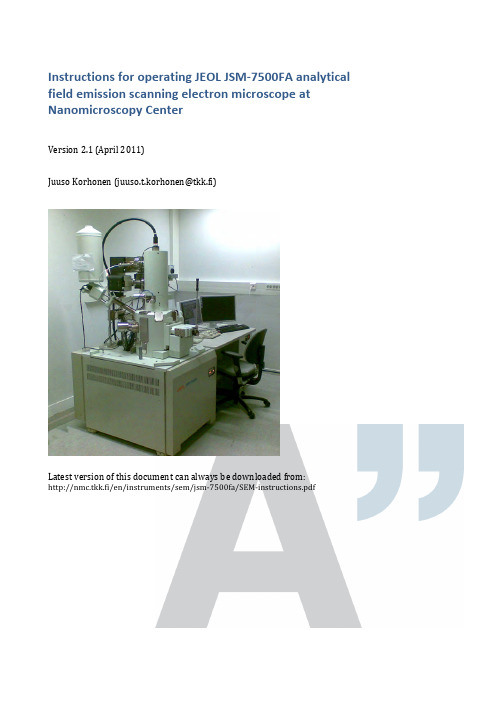
Instructions f or o perating J EOL J SM-‐7500FA a nalytical field e mission s canning e lectron m icroscope a t Nanomicroscopy C enterVersion 2.1 (April 2011)Juuso K orhonen (***********************)Latest v ersion o f t his d ocument c an a lways b e d ownloaded f rom:k.fi/en/instruments/sem/jsm-‐7500fa/SEM-‐instructions.pdfOfficial i nformationNew u ser t rainingInexperienced u sers h ave a c ouple o f o ptions, l isted b elow i n t he o rder o f preference.1.Ask f or t raining f rom t he m ost e xperienced S EM u ser o f y ourresearch g roup.2.Attend t o t he c ourses T fy-‐125.4313 a nd T fy-‐125.4314 M icroscopyof n anomaterials (5+5 c r). T hey a re l ectured e ach s pring b y P rof.Janne R uokolainen.3.Ask o ne o f t he a dministrators t o a rrange a t raining s ession.a.Small g roups o f 2-‐3 p eople a re p referred f or t he t rainings.Allow s ome t ime t o g ather e nough p eople f or t he g roup.b.Training i s d one u sing a p ractice s ample a nd p ersonalsamples a re u sually n ot i maged.Experienced u sers c an c ontact o ne o f t he a dministrators f or a s hort introduction t o t he e quipment.Every n ew u ser h as t o b e a pproved b y o ne o f t he a dministrators b efore t hey are a llowed t o u se t he S EM o n t heir o wn. T he a dministrator k eeps a s hort (15-‐30 m in) s ession w here t he e ssential s kills o f t he u ser a re c hecked. User a pplicationUser a pplication h as t o b e f illed i n o rder t o g ain r eservation a ccess t o a ny o f the N MC e quipment. T he f orm c an b e f ound f romk.fi/en/documents/nmc_user_application_form.pdf a nd i t i s returned t o o ne o f t he a dministrators f or a pproval.PricingBilling i s d one u sing t he c urrent N MC p rice l ist. C ontact P rof. J anne Ruokolainen f or t he m ost c urrent l ist. P lease n ote t hat i ndividual t raining given b y t he a dministrators w ill a lso b e c harged.Precautions – r ead c arefully•Always c heck t he l iquid n itrogen l evel a nd f ill i f n ecessary.o First u ser o f t he d ay a lways f ills t he t ank.•Keep a ll p arts c lean a nd c lean t hem i f n ecessary w ith e thanol.o Wear g loves w hen h andling h olders.•Fill t he l og b ook o n t he c omputer.o Mark a ny s trange b ehavior o r p roblems t o t he l og b ook.•If s omething i s m issing f rom t he S EM o r f rom t he s ample p reparation room (e.g. g loves, e thanol, h olders, c arbon t ape), p lease i nform o ne o fthe a dministrators (send e mail o r c all).•Use o nly f eatures y ou a re t rained t o u se. F or e xample, d o n ot u se EDS o r R BEI i f y ou d on’t k now h ow t o o perate t hem s afely.•Use o f U SB s ticks i s s trictly p rohibited d ue t o s ecurity i ssues a nd hardware i ncompatibility.•Stay c alm a nd u se y our c ommon s ense.•Contact a dministrators i f y ou a re i n d oubt. C ontact i nformation i s found o n t he l ast p age o f t hese i nstructions.Quick s tartup p rocedure1.Turn o n b oth m onitors a nd c heck t hat S EM s oftware a nd u sage l og(Excel) a re r unning. S tart t hem i f n ecessary. L og i n a s G uest (nopassword).2.Check t he l iquid n itrogen l evel a nd f ill i f n ecessary. T he f irst u serof t he d ay a lways f ills t he t ank.3.Fill t he u sage l og:a.Date, s tart t ime (and e nd t ime).b.Your n ame (and t he n ame o f y our h ost i f y ou d o n ot h avereservation p ermissions).c.Vacuum l evels b efore s tarting.d.Amount o f f illed l iquid n itrogen (write “0” i f y ou o nlychecked t he l evel).e.Write n otes a nd c omments t o t he l ast f ield i s n ecessary.f.Save t he f ile (Ctrl-‐S).4.Prepare y our s ample.5.Insert s ample i nto m icroscope:a.Press E xchange p osition.b.Press a nd h old V ENT f or c a. 1 s ec. O pen s ecuring l atch. W ait.c.Open c hamber a nd i nsert h older a long t he d irection o f t hearrows.d.Close c hamber.e.Press a nd h old E VAC f or c a. 1 s ec. W ait u ntil b linking s tops.f.Operate t he r od t o m ove t he s ample t o t he s tage. I f y ou’re n otabsolutely c ertain h ow t o d o t his, r ead t he d etailedinstructions!g.Take o ut t he r od.6.Wait u ntil v acuum l evel r eaches l ess t han 5⋅10-‐4 P a.7.Set E mission c urrent t o 10 μA.8.Select A cceleration v oltage.9.Press O bservation O N.Shutdown p rocedure1.Press O bservation O FF t o t urn o ff a cceleration v oltage.2.Press E xchange p osition.3.Take o ut h older u sing t he r od.4.Press a nd h old V ENT f or c a. 1 s ec. O pen s ecuring l atch. W ait.5.Open c hamber a nd t ake o ut t he h older.6.Close c hamber.7.Press a nd h old E VAC f or c a. 1 s ec.8.Mark e nding t ime a nd o bservations t o U sage l og a nd s ave f ile (Ctrl-‐S).9.Set S EM M onitor s oftware t o n ormal s ettings:a.Exchange p osition p ressed (green).b.Mode: S EMc.Magnification: m inimum f or b oth S EM a nd L Md.Probe c urrent: 810.Turn o ff s pecial f eatures y ou h ave u sed: I mage r otation, d ynamicfocus, e tc.11.If y ou m ade a ny c hanges i n t he O peration S ettings m enu, c hangethem t o n ormal v alues (scan s peeds, i mage f unction, e tc.).12.Clean t he h olders w ith e thanol i f n ecessary.13.Clean t ables. I f y ou w ant t o s tore y our s amples, m ark t hem w ith y ourname a nd p ut t hem o nto a s helf. T hings l eft o n t he t able a re t hrowninto t he t rash.14.Transfer y our i mages f rom t he s mall c omputer o n t he b ack t able.You c an f ind y our f iles a t t he n etwork d rive c alled H arley.e U SB s tick, S SH, e mail, o r b urn a C D.b.The f iles c annot b e t ransferred d irectly f rom t he S EMcomputer d ue t o s ecurity r easons.15.Turn o ff m onitors. D o n ot l og o ut f rom t he s oftware o r c lose t heExcel l og b ook.Changing s ample1.Press O bservation O FF t o t urn o ff a cceleration v oltage.2.Press E xchange P osition t o m ove t he s tage t o c orrect p osition.3.Take s ample o ut b y o perating t he r od.4.Press a nd h old V ENT f or c a. 1 s ec. t o f lush c hamber a nd o pen l atch.Wait.5.Open c hamber a nd t ake o ut s ample (pull a long t he a rrows, n ot u p).6.Change s ample a nd i nsert h older a long t he a rrows.7.Close c hamber a nd s ecure w ith l atch.8.Press a nd h old E VAC f or c a. 1 s ec. W ait u ntil b linking s tops.9.Insert s ample b y o perating t he r od. T ake o ut r od.10.Wait u ntil c hamber v acuum r eaches 5⋅10-‐4 P a b efore t urning o nacceleration v oltage.Special f eaturesThis i s o nly a q uick r eference. S pecial t raining i s r equired t o u se R BEI o r E DS, because o f s afety i ssues.Infrared c ameraYou c an s ee i nside t he c hamber u sing t he i nfrared c amera.1.Switch c amera o n f rom t he b utton o n t he t able.2.From S EM s oftware s elect N avigator -‐> I nfrared c amera3.Turn c amera o ff w hen u sing R BEI o r E DS.Probe c urrent m eterProbe c urrent m eter c an b e u sed t o c heck t he c urrent g oing t o t he s ample. I t is m ost i mportant i n E DS a nalysis.1.Insert t he d etector b y c hecking P CD f rom t he b ottom r ight c orner o fSEM s oftware.2.Take o ut d etector a fter y ou h ave r ead t he c urrent f rom t he S EMsoftware.Retractable b ackscattering d etector (RBEI)Backscattering d etector i s u sed t o d istinguish b etween e lements o n t he sample.1.Set w orking d istance t o 8 m m o r m ore.a.Inserting R BEI w ith l ess t han 8 m m b etween t he s ample a ndthe o bjective l ens w ill r esult i n s erious d amage.2.Turn o ff i nfrared c amera.3.Insert d etector b y c hecking R BEI f rom t he b ottom r ight c orner o f t heSEM s oftware.4.Select C OMPO o r T OPO f or i mage m ode (same m enu a s S EM a nd L M)and u ser a s low s canning s peed f or o bservation.X-‐ray a nalysis (EDS)This g uide i s n ot a dequate f or p roper o peration o f E DS, b ut i s o nly a q uick reference f or t rained u sers.1.Set w orking d istance t o e xactly 8 m m.a.Focus w ith Z h eight u sing t he r ing o f t he s croll w heel i nsteadof F OCUS.2.Insert R BEI.3.Turn o n b ias v oltage b y c licking t he l ightning i ndicator.a.Wait u ntil c ount r ate s tabilizes.4.Select A nalysis f rom t he r ight s ide o f S EM s oftware.5.Click D T (dead t ime) a nd s elect T4 f rom t he l ist.6.Adjust p robe c urrent s o D T b ecomes g reen (around 20-‐30 %) a ndcount r ate i s c a. 2000-‐3000 c ps.7.Take s pectra, l ine s can, o r m apping u sing t he a ppropriate b uttons.8.When a sked a bout s aving t o a n etwork d rive, s elect O K.9.Save t he a nalysis b efore e xiting a nalysis m ode i n o rder t o b e a ble t oreturn t o t he a nalysis l ater.a.Exporting o nly s aves t he i mage a nd y ou c annot r eturn t omake m ore a nalysis o n t he d ata.10.When y ou a re f inished w ith a nalysis, t urn o ff t he b ias v oltage a ndtake o ut R BEI.Saving E DS s pectraIf y ou w ant t o b e a ble t o p lot y our E DS s pectrum, s elect E xport a nd t hen select M SA f ile. I t w ill s ave t he s pectrum i n a c ompatible f ile f or u se i n O rigin, Excel, o r s ome o ther p lotting p rogram.Detailed i nstructionsOperating t he r od (sample e xchange m echanism)This p rocedure d escribes h ow t o u se t he s ample e xchange m echanism i norder t o e ither r emove o r i nsert a s ample h older i nto/from t he m icroscope.Read t his s ection c ompletely t hrough b efore p roceeding a nd m ake s ure t hatyou u nderstand e very s tep.Precondition: T he e xchange c hamber i s i n v acuum a nd t he d oor s eparatingit f rom t he m icroscope i s o pen. C onfirm t hat E VAC l ight i s l it a nd n otblinking. D epending o n w hether y ou a re i nserting o r t aking o ut a s ample, t heholder m ight b e i n t he e xchange c ompartment (HLDR l ight i s o ff) o r i nsidethe m icroscope (HLDR l ight i s o n).See t he v ideo o n t he c omputer d esktop f or a d emonstration. U PDATE: T hefigures a re f rom a n o ld v ersion o f r od.1.Push t he b ar i nside t he m icroscope b y f ollowing t he p rocedure:a.Lower t he r od t o h orizontal l evel, w hile l ightly h olding i tback.b.Let t he r od b e p ulled i n s lowly.c.Push t he b ar g ently a ll t he w ay i nside u ntil i t s tops (d).•There i s a l ittle r esistance a t t he f inal c ouple o fcentimeters.•The s ample s hould b e n ow e ither r eleased f romthe b ar o r a ttached t o i t (depending o n w hetheryou a re i nserting o r r emoving t he h older).•If y ou h ave n ot p ushed t he s ample a ll t he w ayinside a nd s tart t o p ull b ackwards t here i s adanger t hat t he s ample h older w ill f all t o t hebottom t he s ample c ompartment. I f t his h appens,the w hole s ample c ompartment h as t o b e o pened.Contact S EM a dministrators i n t his c ase.2.Pull t he b ar o ut f rom t he m icroscope u sing t he f ollowingprocedure:a.Pull t he b ar o ut a s f ar a s i t c omes (e).•The t wo a rrows o n t he h older s hould a lign w iththe p ipe e nd.•If y ou h ave n ot p ulled f ar e nough, t he r od m ightbe d amaged d uring t he l ift.b.Lift t he r od u pwards t o v ertical.•Now y ou s hould e ither h ave t he s ample i nside t hemicroscope o r i n t he e xchange c ompartment a ndthe e xchange c ompartment i s i n v acuum.Opening t he s ample e xchange c ompartmentThe f ollowing p rocedure d escribes h ow t o b ring t he e xchangecompartment t o a tmospheric p ressure.Precondition: T here i s n o s ample i nside t he m icroscope o r i t h as b eenbrought t o t he e xchange c ompartment, a nd t he e xchange c ompartment i sin v acuum. F irst c heck t hat H LDR l ight i s o ff o n t he s ample e xchangecompartment (i.e. t here i s n o s ample i nside t he s ample c ompartment).Figure. S ample e xchange r od1.Pressurize t he e xchange c ompartment:a.Press a nd h old (for a bout 1 s econd) t he V ENT b utton o n t heexchange c ompartment.i.The b utton s tarts t o b link a nd y ou h ear s ome s ounds.ii.In a f ew s econds, t he d oor b etween t he e xchangecompartment a nd t he s ample c ompartment c loses.You c an o bserve t his b y e ar a nd b y l ooking a t t hebottom r ight c orner o f t he S EM M onitor.2.Open t he l atch a s s oon a s y ou h ear t he c lick.3.Open t he e xchange c ompartment d oor (it s hould o pen a lmost b yitself).a.You d o n ot n eed t o w ait u ntil t he p umping h as s topped.b.The c ompartment w ill c ontinue p urging f or a f ixed a mount o ftime. Y ou d o n ot h ave t o w ait u ntil i t s tops a nd y ou c anevacuate i t a s s oon a s y ou l ike.4.Now y ou h ave t he s ample c ompartment o pen a nd r eady f orloading/unloading t he s ample h older.Inserting a s amplePrecondition: T here i s n o s ample i nside t he s pecimen c hamber a nd exchange c ompartment i s i n v acuum. F irst c heck t hat H LDR l ight i s o ff o n the e xchange c ompartment (i.e. t here i s n o s ample i nside).1.Move t he s tage t o e xchange p osition:a.Click E xchange P osition o n t he S EM M onitor.i.If b utton i s n ot v isible, c lick "Specimen" f rom t herightmost e dge o f S EM M onitor.ii.Make s ure t hat E XCH P OSN i s l it o n t he e xchangecompartment, b efore p roceeding.2.Bring t he e xchange c ompartment t o a tmospheric p ressure b yfollowing p rocedure i n s ection “Opening t he s ample e xchangecompartment”. Q uick n otes:a.Press a nd h old V ENT f or c a. 1 s ec.b.Open l atch. W ait.c.Open c hamber d oor.3.Put o n g loves i f y ou d o n ot h ave t hem a lready o n.a.Parts t hat a re i n c ontact w ith t he v acuum s hould b e k eptabsolutely c lean. I f y ou h ave t ouched s ome p art, c lean t he p artwith e thanol (not a cetone).4.Insert h older t o t he s pecimen c huck:a.Slide t he s pecimen h older i nto t he s pecimen c huck a long t hearrow d irection o n t he s pecimen h older.5.Check t hat t he O-‐ring s eal o n t he d oor i s O K a nd w ipe i t w ith a c leanglove i f n eeded t o g et r id o f a ny d ust.a.If t he r ing i s r eally d irty, w ipe i t w ith e thanol o r i sopropanol(do n ot u se a cetone o r m ethanol).6.Close t he c hamber d oor a nd s ecure i t w ith t he l atch.7.Evacuate t he c ompartment b y p ressing a nd h olding E VAC (forabout 1 s econd). T he l ight w ill s tart b linking.a.Wait u ntil t he l ight s tops b linking a nd t he d oor s eparatingthe e xchange c ompartment i s c losed. Y ou c an o bserve t hisfrom t he b ottom r ight p art o f t he S EM M onitor.8.Insert t he s ample h older i nside t he m icroscopea.Refer t o s ection “Operating t he r od” i f i n d oubt.9.A p opup w indow s hould a ppear o n t he S EM M onitor. N ow s elect t heappropriate h older a nd s et t he o ffset v alue.a.If p opup d oes n ot a ppear, t ake o ut t he h older a nd i nsert i tagain.10.Wait u ntil t he v acuum l evel r eaches 9.6·10-‐5 P a (if t hat i s n otpossible, w ait a t l east u ntil 5·10-‐4 P a).Taking o ut s amplePrecondition: T here i s a s ample i nside t he m icroscope a nd e xchange compartment i s i n v acuum. F irst c heck t hat H LDR l ight i s o n o n t he s ample exchange c ompartment (i.e. t here i s a s ample i nside) a nd E VAC l ight i s o n and n ot b linking.1.Click O bservation O FF t o t urn o ff a cceleration v oltage.2.Click E xchange P osition t o m ove t he s ample h older t o t he e xchangeposition.a.Make s ure t hat E XCH P OSN i s l it o n t he e xchangecompartment b efore p roceeding.3.Bring t he s ample t o t he e xchange c ompartment b y o perating t herod.a.Refer t o s ection “Operating t he r od” i f y ou a re n ot a bsolutelycertain h ow t o d o t his.4.Pressurize t he e xchange c ompartment:a.Press a nd h old V ENT f or c a. 1 s ec u ntil i t s tarts t o b link.b.Open s ecuring l atch. W ait.c.Open c hamber d oor.5.Now y ou h ave t he s ample c ompartment o pen a nd y ou a re r eady t akeout y our s ample. I f y ou a re d one w ith t he i maging, j ust c lose t heexchange c hamber a nd e vacuate i t o therwise c ontinue w ith i nsertinga n ew s ample. D o n ot l eave t he c hamber o pen f or a l ong p eriod o ftime, b ut e vacuate i t i f n eeded.Sample h oldersSample h olders c onsist o f a b ase p art a nd a n a dapter p art (show o n t he f igure right). T here a re t hree d ifferent a dapters f or d ifferent s pecimen s tubs s hown in t he f igure b elow (a, b , c , d ).The m ost b asic h olders a re t he 12.5 m m (b-‐1) a nd 25 m m (c-‐1) a luminum “JEOL” s tubs . T hey s hould b e u sed w henever p ossible. S tubs s hould a lways b e available a t t he s ample p reparation r oom, b ut y ou c an a lso o rder y our o wn ones e .g. f rom E MS (order n umbers 75730, a nd 75700). T he u se o f r egular holders i s i ncluded i n t he o peration p rice o f t he m icroscope.Also “mini-‐stubs” a re a vailable f or u se w ith a p rovided a dapter. T hey a re preferred f or s mall s amples. T hey c an b e o rdered f rom T ed P ella (order numbers 16180, a nd 16181).For s pecial o ccasions, a H itachi a dapter (a) c an b e u sed. S pecial c are m ust b e taken w hen u sing t hese h olders, b ecause t hey l ack s ome s afety f eatures. Ask a dministrators, i f y ou h ave s pecial r equests f or h olders. T here a re a lso different k inds o f c ross-‐section h olders a vailable. A sk t he a dministrators f or more i nformation.Attaching a dapter t o b ase p arta) Make s ure t hat p arts a re n ot d irty, c lean i f n ecessary. b) Place a dapter o n t he b ase p art.c) Tighten s crew o n t he b ase p art l ightly.Figure. A ttaching a dapter t o base p art.Figure. 12.5 m m a nd 25 m m "JEOL" stubs.Figure. "Mini-‐stubs" a nd 12.5 m m a dapter.Figure. C ross-‐section holders.Sample h eightAlign t he t op o f t he s ample w ith t he g roove i nside t he J EOL a dapter p art. U se the s crew o n b ottom t o r aise o f l ower t he s ample. W hen u sing a nother holder, m ake s ure t hat h eight f rom t able t op l evel i s e xactly 25 m m.CoatingFor n on-‐conductive s amples a c oating i s u sually n eeded f or o bservation i n SEM. T his c an b e e asily p erformed b y u sing s putter c oating o f g old, p latinum, or g old-‐palladium. T here i s a s putter c oater a t N MC, w hich c an b e u sed f or this p urpose. R esolution l imiting f actor i s t he g rain s ize, w hich i s u sually 5-‐20 nm d epending o n t he c onditions o f s puttering.Also c arbon c oating c an b e u sed t o m ake s amples c onductive. I t i s a nappealing m ethod, w hen d oing X -‐ray a nalysis. I t c reates a v ery u niform l ayer without n oticeable grains.Figure. A lign t op o f stub w ith t he g roove on t he s ample holder.Basic m icroscope o perationBasic c onceptsWorking d istance a nd Z v alueWorking d istance (WD) v alue s ets t he e ffective f ocal l ength o f t he o bjective lens.Z h eight v alue s ets t he d istance o f t he (supposed) s urface l evel o f t he s ample from t he o bjective l ens.These t wo v alues a re e qual, w hen t op o f s ample i s a ligned w ith t he t op o f the h older (ie. 25 m m h igh f rom t able l evel, s ee f igure). W D > Z, i f y our sample i s l ower t han t he c orrect l evel a nd v ice v ersa. I f W D < Z y ou n eed t o set t he S ample O ffset v alue a ccordingly.Sample o ffsetThe h eight o f t he t op l evel o f t he s ample m easured f rom t able t op l evel should b e e xactly 25 m m. T he s ample c an b e s et a lso 0-‐4 m m h igher t han t he nominal l evel, b ut t hen t he S ample O ffset v alue h as t o b e s et a fter i nserting sample. I t i s l ocated a t t he b ottom o f t he s ample h older s elect w indow, w hich pops u p a utomatically a fter h older i nsert.Acceleration v oltage, e mission c urrent, p robe c urrent…The f irst t hing t o t hink a bout w hen s tarting i maging i s t he s election o f acceleration v oltage. T he c hoice d epends o n t he t ype o f t he s ample. S ee table b elow f or s ome e xamples.Sample Observation c ondition NotesGold p articles o n conductive s urface 5-‐30 k V, p robe c urrent a t c a. 10, working d istance 1.5-‐8 m mCoated p orous polymer 1-‐5 k V, p robe c urrent 6-‐10, w orking distance 4.5-‐8 m mUncoated p olymer 0.5-‐1 k V, p robe c urrent < 8, g entlebeam m ode, w orking d istance c a. 8mmCoated b iological sample 1-‐5 k V, p robe c urrent c a. 10, w orking distance 4.5-‐25 m m d epending o n feature s izeUncoated p aper 1-‐2 k V, g entle b eam (GB-‐L) m ode,working d istance 4.5 m m, p robecurrent 6-‐10.Coated p aper 5 k V, w orking d istance 4.5-‐25 m m,probe c urrent c a. 10X-‐ray a nalysis o f conductive s ample 15-‐30 k V, w orking d istance e xactly 8mm, h igh p robe c urrentRetractable B EIdetector i nsertedX-‐ray a nalysis o f poorly c onductive sample 5 k V, w orking d istance e xactly 8 m m,probe c urrent a s h igh a s p ossibleRetractable B EIdetector i nsertedThe e mission c urrent i s t he c urrent d rawn f rom t he e mitter. S et i t a lways t o 10 μA. Figure. S ample height s hould b e exactly 25 m m measured f rom t able top l evel.Probe c urrent i s t he c urrent d irected a t t he s ample. H igher v alues g ive better s ignal t o n oise r atio, b ut c ause m ore c harging a rtefacts i n p oorly conducting s amples. V alue o f 8-‐10 i s u sually a g ood c hoice.AligningUsually t he m icroscope i s a ligned w ell e nough f or m icrometer s cale operation. I n t his c ase, o nly f ocusing i s n ecessary. F or h igher m agnification work, t he e lectron b eam n eeds t o b e a ligned a nd a stigmatism o f t he o bjective lens h as t o b e c orrected.FocusThe f irst l evel o f a ligning i s a lways f ocusing. F ocusing i s d one u sing t he FOCUS k nob o n t he o peration c onsole. C lockwise r otation i s u nder f ocus (weaker l ens) a nd c ounterclockwise i s o ver f ocus (stronger l ens).If p ossible s elect s ome f eature, w hich y ou c an u se i n t he m agnification r ange from c a. 1000 t o 20000.Start f rom a l ow m agnification a nd w hen y ou g et g ood e nough i mage m ove on t o h igher m agnification f or f ocusing. I t t he a lignments a re r eally o ff, y ou might n ot g et a c lear i mage a t a ll.Beam a lignBeam a lign i s a lways d one a t p robe c urrent 8. S elect t he c orrect p robe current v alue f rom t he s oftware.Press A LIGN o n o peration c onsole. T he i mage s tarts t o m ove o n t he s creen. Use t he X a nd Y k nobs t o m inimize t he m ovement. P ress A LIGN O FF (STIG) button w hen i mage h as s topped. R epeat f or m agnifications u p t o c a. 20000. Focus t he i mage w henever n ecessary.Astigmatism c orrectionTo c orrect t he o bjective l ens a stigmatism p ress t he S TIG b utton o n t he operation c onsole (it i s u sually a lready s elected a t t his p oint). M ove o n t o a spherical f eature, w hich y ou a re a ble t o o bserve a t m agnification 10000 o r more.Move t he F OCUS k nob s o t hat y ou g o f rom u nderfocus t o o verfocus a nd b ack several t imes. W hen y ou h ave a stigmatism, t he i mage g ets e longated i n diagonal d irections w hen m oving a round t he f ocal p oint. S elect t he f ocal point w here n o e longation o ccurs.Adjust t he X a nd Y k nobs s o t hat y ou g et t he c learest i mage p ossible. F ocus whenever n ecessary.Other c orrectionsThere a re a lso o ther a lignments, s uch a s s ource a lign, c ondenser l ens astigmator, l ow m agnification c enter, a nd s tigmator c enter c orrections. These v alues s hould n ot u sually b e c hanged a nd t heir u se i s n ot d escribed here.Problems a nd t roubleshootingAnswers t o c ommon p roblemsI w ant t o u se U SB s tick t o t ransfer m y f iles!You c an t ransfer y our f iles t o a U SB s tick f rom t he s mall c omputer a t t he b ack wall. Y ou’ll f ind y our f iles u nder t he n etwork d rive H arley.Help! T here i s n o i mage.Follow t he c hecklist t o f ind t he c ause:1.Are y our Z a nd W D v alues t he s ame? I f n ot p ress W D t o s et c orrectdistance.2.What d etector a re y ou u sing? I f W D<8 m m y ou u sually d o n ot g etimage w ith L EI d etector; a nd i f W D>8 m m S EI g ives o nly s tatic n oise.LM m ode s hould w ork f ine i n t his c ase.3.What i s y our p robe c urrent v alue? I f i t i s l ow, t ry i ncreasing i t.4.If n one o f t he a bove i s t rue, t ry r esetting a lignment. G o t o A lignmentpanel a nd c lick R eset A ll.a.In a r eally b ad c ase t he s ource a lignment h as g one b ad.Contact a n a dministrator t o a lign i t.If t here i s n o i mage w hen s tarting o perationFirst, p ress A CB (auto c ontrast & b rightness). I f y ou e ven s ee s ome s tatic noise, y ou o nly n eed t o f ind t he c orrect f ocal p oint. S ee p revious s ection.In c ase y ou h ave c ompletely b lack s creen w hen y ou s tart i maging, f ollow t he list u ntil y ou h ave i mage.1.Restart o f S EM s oftware:a.File-‐>Exit t o g o t o l ogin s creen.b.Close l ogin s creen f rom E xit b utton.c.Wait o ne m inute.d.Start S EM_Monitor s oftware.e.Log i n a s G uest.2.Restart c omputer:a.Close S EM s oftware.b.Save E xcel l og b ook a nd e xit.c.Restart W indows.d.Start S EM s oftware a nd E xcel l og b ook.3.Restart o peration c onsole:a.Read i nstructions b elow.If v acuum b reaks d uring s ample e xchangeVacuum u sually b reaks i f t he l ever i s p ushed o r t wisted d uring t he s ample insertion. T he c omputer w ill r aise a m aintenance w indow s howing e rror messages. T he m icroscope w ill a utomatically s hut d ownsome p arts a nd t he v acuum p umps h ave t o b e r estarted. B ring t he microscope b ack t o i ts n ormal c ondition b efore p roceeding. F or e xample, lift t he r od b ack t o i ts u pright p osition.1.Locate t he t wo V AC S W b uttons b elow t he t able. T here a re a lso M AINSW b uttons, b ut d o n ot t ouch t hem.2.Shut d own v acuum p umps b y p ressing V AC O FF (0=OFF, 1=ON)button. T he p umps s hould n ow s top, i f t hey w ere n ot s hut d ownalready.3.Wait a m oment a nd r estart p umps b y p ushing V AC O N b utton.a.There i s a 20 m in t imer f or s tarting t he p umps s o y ou w illhave t o w ait a t l east 20 m inutes b efore p roceeding.4.After a ll o f t he e rror m essages h ave d isappeared f rom t he d isplay,you c an c ontinue o perating.Turning o ff c omputer1.Log o ut f rom t he S EM s oftware (File-‐>Exit).2.Save t he E xcel l og b ook (File-‐>Save o r C trl-‐S).3.Close t he E xcel l og b ook.4.Select S hutdown f rom S tart m enu.Powering o n c omputer1.Start c omputer f rom t he p ower s witch.2.Log i n a s S EMUser (password: S EMUser).3.Start E xcel l og b ook b y d ouble c licking “SEM U sage L og” o n t he r ightmonitor d esktop.4.Start S EM s oftware b y d ouble c licking S EM_Monitor.5.Log i n a s G uest.Restarting o peration c onsole1.Turn o ff c omputer.2.Press O P S W O FF f rom b elow t he t able.3.Wait c a. 10 s econds.4.Press O P S W O N.5.Turn o f c omputer.6.Wait a c ouple o f m inutes b efore s tarting S EM_Monitor s oftware.。
超高分辨率场发射扫描电子显微镜JSM-7800F介绍

加速电压 :1.5kV 工作距离(WD):2mm 过滤器电压:-1400V 探测器:UED
背散射电子为主
19
Copyright (C) JEOL Ltd., All Rights Reserved.
SHL
②最适合于磁性材料和EBSD分析的电子光学设计
〈应用实例〉
1. 磁性材料分析:Fe3O4 纳米颗粒集合体 2. EBSD晶体取向分析:钕铁硼 3. EBSD晶体取向分析:碳钢
0.25 μm
应用实例3. 碳钢 EBSD 图像
1000倍IQ(图像质量)图像 1000倍 ND方向图像
也适合于磁性材料的高精度晶体取向分析
加速电压:20 kV WD:20mm 探针电流:8 nA 100 nm 步长 样品:碳钢(S25C)直径:32 mm 高度:20 mm 样品制备:金刚石砂轮研磨、胶体二氧化硅抛光
应用实例1. 碳上的镀金颗粒
极低加速电压图像 80 V JEOL Only
JSM-7800在80V的电压下也能观察高品质的图像 通过观察样品表面可以进行纳米结构的分析
8万倍
12万倍
16
Copyright (C) JEOL Ltd., All Rights Reserved.
应用实例2.
石墨烯
极低加速电压图像 80 V
out-lens
稳定度・重现性 高加速 分辨率
观察 磁性 材料
EBSD EDS/WDS
低加速 分辨率
低倍率观察
低倍率观察
13
Copyright (C) JEOL Ltd., All Rights Reserved.
超级混合式物镜(SHL)的功能评估
超级混合式物镜 semi-in-lens
场发射扫描电子显微镜参数
场发射扫描电子显微镜参数:1.工作条件:1.1电源: 230V (-6%/+10%) / 50Hz (±1%)1.2 主机功耗:< 3.0 kV A1.3运行环境温度: 17-23 C1.4运行环境:相对湿度< 80% (无冷凝)1.5残余交流磁场<100nT (非同步频率);<300nT (同步频率)1.6噪音:< 60 dBC1.7干燥无油压缩空气4-6 bar1.8仪器运行的持久性:可连续运行2.设备用途:2.1高分辨扫描电子显微分析系统主要用于纳米材料的超高分辨微观形貌观察和微区分析。
独特的双物镜设计以及低电压成像技术,对导电性不好的样品等适用性更强。
具有低真空功能,对不导电样品进行更全面的分析。
3.技术规格3.1 电子光学系统3.1.1 分辨率:二次电子(SE)像*3.1.1.1高真空模式:15 kV时优于1.0 nm;1 kV时优于1.4 nm(非减速模式)*3.1.1.2 低真空模式:30kV时优于1.5nm*3.1.2背散射(BSE)像:100V时优于3.5 nm3.1.3 放大倍率范围:1 ~1,000,000倍(根据加速电压和工作距离的改变,放大倍数自动校准)3.1.4 着陆电压:50V 至30 kV3.1.5 电子枪:高稳定度Schottky肖特基场发射电子枪*3.1.6电子束流:0.6pA ~200 nA,连续可调,既保证对高分子纳米材料高分辨成像所需的低速流,也要保证EDS和EBSD分析所需的高束流高效率。
3.1.7 束流稳定性:每10小时< 0.4%*3.1.8 具有双物镜系统(电磁透镜和静电透镜),保证对纳米材料、不导电有机无机材料、合金、磁性材料的全方位分析*3.1.9 物镜光阑:物镜光栏应能自加热自清洁;无需拆卸镜筒即可更换物镜光阑。
至少6孔光阑设计3.1.10 电子束位移范围:不小于±110um3.2 样品室和样品台3.2.1 样品室尺寸:不小于360mm×360mm*3.2.2 抽屉式大开门结构,样品台安装在仓门上,全方位观察,方便取放样品,防止碰撞3.2.3样品台:五轴运动全对中样品台,有效移动范围:X /Y ≧110mm,Z ≧25mm,T = -10°to +70°,R= 360°连续旋转3.2.4样品台最大承重量不小于2.0 kg3.2.5最大样品高度不小于65mm,分析工作距离不小于5mm3.2.6重复精度:2um (X/Y 方向),步进进度优于100nm3.2.7至少15个探测器/附件接口(所有端口程序均免费开放,可安装能谱、波谱、EBSD、CL、STEM探头、红外探头、拉曼等),方便后期升级*3.3 探测器:3.3.1 电子探头:样品室二次电子检测器极靴内二次电子探测器极靴内背散射电子探测器低真空二次电子探测器3.3.2 样品室镜头安装背散射电子探测器3.3.3 样品室IR-CCD相机3.3.4样品室光学显微镜导航相机探头3.4 真空系统*3.4.1完全无油真空系统(标配高真空模式和低真空模式,要求有验收指标)3.4.2 一个220L/S的涡旋干泵和一个分子泵3.4.3 两个离子泵*3.4.4 穿过透镜的压差真空系统(列出原理),保证真空条件下避免对系统的污染。
A包场发射扫描电镜技术要求.

A包:场发射扫描电镜技术要求1.运行环境:房间温度:15~25℃相对湿度:小于60%电源:单相,220V±10%,50/60Hz地线:独立地线2.技术指标2.1 设备组成场发射扫描电子显微镜、能谱仪、离子溅射仪。
2.2场发射扫描电子显微镜2.2.1主机组成:包括真空系统、电子光学系统、各种检测器、自动变压器(若需要)、冷却循环水系统、稳压电源、不间断电源,计算机,标准工具及附件。
2.2.2 技术参数电子枪:场发射电子枪分辨率:1.2nm及以上加速电压:0.5~30kV放大倍率: 20~800k及以上,粗、细调模式连续可调真空系统:(无油)机械泵、分子泵、离子泵三级真空,样品室真空<10-4Pa探测器:二次电子检测器(包括低位、高位)背散射电子检测器CCD 摄像机附件接口:在样品室上提供5个以上附件接口,可同时接X射线能谱仪、波谱仪、EBSD、背散射电子探测器等。
其它:设备必须具有低真空、环扫、着落电子减速模式等功能中的一种。
2.2.3 样品室和样品台:样品台驱动: 3轴马达驱动及以上移动范围:X:0~50mm;Y:0~50mm;Z:0~30mm;T:-3~70°以上;R:360°连续最大样品尺寸:100mm及以上样品置换时间(抽真空时间):不大于7分钟2.2.4计算机E7400/2G/250G/256M/22LCD*2/DVD-RW操作系统:Microsoft Windows XP外界接口:串行、并行、SCSI、USB 2.0接口、网络。
全功能电镜控制操作软件、图像分析软件打印机:HP2015dn2.2.5 图像采集、储存扫描速度:快扫描等于或优于25桢/秒慢扫描全屏模式下慢扫描速度可选,扫描速度0~80秒及以上图像储存:最大像素≥2560×1920图像文件格式:BMP,JPEG,TIFF数据记录:加速电压,标尺或放大倍率,时间,采集的信号电子图像移动:≥±12μm2.2.6 保护具有断电、漏电、真空保护2.2.7标准附件及工具标准随机附件及工具1套灯丝2~4根(以满足10年电镜工作的要求)更换光阑1套导电双面铜碳胶带各10盒2.3 能谱仪2.3.1 组成:主机、计算机、打印机2.3.2 技术指标:制冷方式:电制冷探头面积≥30mm2分辨率优于135eV分析元素范围:4Be~92U及以上最大计数率:≥300000cps可实现点、线、面方式扫描自动元素标定,无标样定量分析2.3.3 计算机E7400/2G/250G/256M/22LCD/DVD-RW操作系统:Microsoft Windows XP外界接口:串行、并行、SCSI、USB 2.0接口、网络。
场发射扫描电子显微镜技术要求解析

附件:场发射扫描电子显微镜技术要求1. 场发射扫描电镜技术规格1.1.分辨率:≤1.0nm(15kV);≤1.4nm(1kV)1.2 加速电压:0.1kV ~30kV1.3 放大倍数:25×~800,000×以上1.4 电子枪:场发射型1.5在样品室上提供不少于六个附件接口,可同时接X射线能谱、背散射电子探测器等。
1.6探测器:普通二次电子检测器高分辨二次电子/背散射电子探测器BSE探测器*1.7样品台:全对中型X方向位移:≥50mm;Y方向位移:≥50mm马达控制:5轴(X, Y, Z, R, T)1.8真空系统前级机械泵配油雾过滤器1.9动态视频保存*2. 配置要求2.1场发射扫描电子显微镜基本单元1台2.2 电镜正常工作所需的稳压电源、循环冷却水、变压器、不间断电源等完整1套2.3备用电子枪1个2.4场发射扫描电镜长期使用所需要的备品备件、专用工具(列详细清单) 完整1套3.售后服务3.1 卖方应在合同生效后的一个月内,对可能的设置室进行地面振动、杂散磁场的测量,并向买方提出详细的安装要求和提供技术咨询。
3.2 仪器到达用户所在地后,在接到用户通知后两周内进行安装调试,直至通过验收。
3.3 设备安装后,在用户现场对用户进行免费培训,培训内容包括仪器的操作和仪器基本维护等,使用户达到独立操作水平。
3.4卖方提供三年的免费保修,保修期自仪器验收签字之日起计算;卖方免费提供软件升级(在不涉及硬件升级的前提下)。
3.5在保修期外软硬件出现问题,应在接到用户通知后两个工作日内给与解决方案或在三个工作日内到达用户现场解决问题。
4.交货期:6个月。
- 1、下载文档前请自行甄别文档内容的完整性,平台不提供额外的编辑、内容补充、找答案等附加服务。
- 2、"仅部分预览"的文档,不可在线预览部分如存在完整性等问题,可反馈申请退款(可完整预览的文档不适用该条件!)。
- 3、如文档侵犯您的权益,请联系客服反馈,我们会尽快为您处理(人工客服工作时间:9:00-18:30)。
场发射扫描电子显微镜参数:
1.工作条件:
1.1电源: 230V (-6%/+10%) / 50Hz (±1%)
1.2 主机功耗:< 3.0 kV A
1.3运行环境温度: 17-23 C
1.4运行环境:相对湿度< 80% (无冷凝)
1.5残余交流磁场<100nT (非同步频率);<300nT (同步频率)
1.6噪音:< 60 dBC
1.7干燥无油压缩空气4-6 bar
1.8仪器运行的持久性:可连续运行
2.设备用途:
2.1高分辨扫描电子显微分析系统主要用于纳米材料的超高分辨微观形貌观察和微区分析。
独特的双物镜设计以及低电压成像技术,对导电性不好的样品等适用性更强。
具有低真空功能,对不导电样品进行更全面的分析。
3.技术规格
3.1 电子光学系统
3.1.1 分辨率:二次电子(SE)像
* kV时优于1.0 nm;1 kV时优于1.4 nm(非减速模式)
* 低真空模式:30kV时优于1.5nm
* nm
3.1.3 放大倍率范围:1 ~1,000,000倍(根据加速电压和工作距离的改变,放大倍数自
动校准)
3.1.4 着陆电压:50V 至30 kV
3.1.5 电子枪:高稳定度Schottky肖特基场发射电子枪
* ~200 nA,连续可调,既保证对高分子纳米材料高分辨成像所需的低速流,也要保证EDS和EBSD分析所需的高束流高效率。
3.1.7 束流稳定性:每10小时< 0.4%
*3.1.8 具有双物镜系统(电磁透镜和静电透镜),保证对纳米材料、不导电有机无机材料、合金、磁性材料的全方位分析
*3.1.9 物镜光阑:物镜光栏应能自加热自清洁;无需拆卸镜筒即可更换物镜光阑。
至少6孔光阑设计
电子束位移范围:不小于±110um
3.2 样品室和样品台
3.2.1 样品室尺寸:不小于360mm×360mm
*3.2.2 抽屉式大开门结构,样品台安装在仓门上,全方位观察,方便取放样品,防止碰撞
,有效移动范围:X /Y ≧110mm,Z ≧25mm,T = -10°to +70°,R= 360°连续旋转
kg
,分析工作距离不小于5mm
(X/Y 方向),步进进度优于100nm
,可安装能谱、波谱、EBSD、CL、STEM探头、红外探头、拉曼等),方便后期升级*3.3 探测器:
3.3.1 电子探头:
样品室二次电子检测器
极靴内二次电子探测器
极靴内背散射电子探测器
低真空二次电子探测器
3.3.2 样品室镜头安装背散射电子探测器
3.3.3 样品室IR-CCD相机
3.4 真空系统
*,要求有验收指标)
3.4.2 一个220L/S的涡旋干泵和一个分子泵
3.4.3 两个离子泵
*3.4.4 穿过透镜的压差真空系统(列出原理),保证真空条件下避免对系统的污染。
3.4.5 样品室真空度:高真空模式优于6×10⁻⁴ Pa,低真空模式优于< 200Pa
3.4.6 抽真空时间:< 210秒
3.5 数字图像处理系统
*,最大扫描和成像6144 x 4096像素
* –25,000µs/像素
3.5.3 图像显示:1920×1200像素,24”LCD显示器显示,能显示和处理图像
*,既能实现同一个显示屏上单个活动窗口全屏显示某一探测器的图像信号,又能在同一显示屏上多个活动窗口(最多不少于4个窗口)同时并列显示不同探测器的图像信号,图像信号可相互实时切换,互不干扰
3.5.5 图像记录:TIFF(8位,16位或24位),BMP或JPEG可选
3.5.6 智能扫描软件,具有:至少256幅的平均或积分,线积分或平均,隔行扫描,漂
移补偿幅积分,伪彩色功能,实时存储图像,图像处理(反像, Gamma,平滑,锐化,增
强等),图像旋转,电子束屏蔽(Beam blank)
3.6 控制和数据处理系统
3.6.1 电镜控制器,最低配置要求:
国际主流品牌计算机工作站,Intel Xeon 四核3.0GHz以上CPU;DDRIII 16.0GB内存;
1000GB硬盘;1G独立专业图像显卡;DVD刻录机;一台1920×1200分辨率的24”LCD 显示器
3.6.2 Windows 7的64位图形操作系统
3.6.3 操作方式:键盘、鼠标
3.6.4 可自动调节:电子枪对中、自动亮度对比度、自动聚焦、自动聚焦消像散、自动
电子束设定、自动合轴、真空控制、动态聚焦、旋转补偿、倾斜补偿等
3.6.6 操作台:原装进口实验台。
3.7 应用软件
3.7.1 应具有样品台图像导航功能
3.7.2 应具有双击鼠标移动样品功能
3.7.3 应具有鼠标拖曳式放大及对中功能
,保证超大视野的图像
,自动引导用户完成高分辨观察、分析等操作
,能测量试件的长宽高、直径、周长、面积等
3.7.9 应提供内嵌式的实时帮助文件,保证操作者的使用直观便捷化。
*3.8 冷却循环单元
3.8.1 采用比空气冷却更高效、更精准控制的水冷内循环系统,分别用于冷却扫描电镜
镜筒及其它部件,高效散热,保证长期使用
3.8.2 电压要求:200 – 230 V AC, 50/60 Hz
3.8.3 温度调节控制范围:+ 5C ~+ 40C
3.8.4 控温精度:± 0.1C
3.8.5 容量:不小于5L
3.8.6 配有进口空压机一套
3. 9 附件
3. 9 .1 UPS稳压电源:1套,国际品牌Times Top,不低于10kV A
3. 9 .2 电子干燥柜:1台,上下双门,容积不低于240L,全自动电子除湿,无尘,无
滴水,无噪音
3. 9. 3 无人基站用直流变频空调:1台,不低于3P,具有除湿功能,且遇停电再恢复
供电后能够自动恢复运转状态;制冷容量不低于7.2kW,制热容量不低于8.0kW
3. 9 .4 冷暖两用空调:知名品牌,1台,挂机,1.5P
3. 9 .5 超声波清洗器:2台,容量为6L;超声功率为150W,频率40kHz;温控范围0~80℃,
加热功率200W;外壳采用优质不锈钢板;1~20分钟内任意设定超声时间
3. 9.6计算机:1套,国际品牌,配置不低于:I5 2.8GHz处理器,4GB内存,1TB硬盘,
独立显卡,DVD 刻录机,22英寸液晶显示器,光电鼠标,黑白激光打印机,满足A4、B5纸张尺寸打印;Windows 7 或以上正版;电脑桌、椅1套。
*3. 10 仪器室配套设施:
保证仪器室磁场、震动、噪音等满足安装要求。
4.产品配置要求
4.1 主机系统一套
4.2 电镜控制计算机一套
4.3 电镜用24寸液晶显示器一台
4.4 样品室二次电子探测器一个
4.5 极靴内二次电子探测器一个
4.6 极靴内背散射电子探测器一个
4.7 低真空二次电子探测器一个
4.8 样品室角度选择背散射电子探测器一个
4.9 样品室红外CCD相机一个
4.10 样品室光学显微镜导航相机探头一个
4.11 随机进口空压机一台
4.12 冷却循环单元(内循环)一台
4.13 导电碳胶带三卷
4.14 导电银浆一瓶
4.15 Win7 64位正版操作系统一套
4.16 MS Office正版系统一套
4.17 备用场发射电子源一套
4.18 备用钼制物镜光阑一套
4.19 进口高分辨测试标准样品一个
4.20 附件一批
需要附件包括:不间断电源、电子干燥柜、无人基站用直流变频空调、冷暖两用空调、计算机,以上附件各一套、超声波清洗器2台。
4.21其它必备备品备件一套
需要备件、特殊工具和消耗品包括:专用工具、物镜光阑、整套密封圈、整套保险丝、闪烁体、真空脂、微动开关、备用集成块、导电胶带等。
标准电镜样品和能谱校正样品。
4.22仪器室配套设施一套
5.技术文件
5.1 合同签订后提供设备的预安装要求说明书;
5.2 随机提供产品使用说明书和维护说明书;
5.3 随机提供完整的产品验收说明书;
5.4 包装箱应用新的坚固的经过熏蒸后的木箱或铁皮箱,能防潮、防锈、防震、防粗暴装卸,适于整体吊装,适于长途运输或转卸装运。