Gate and Base Drives2
H-Bridge Gate Driver HIP2101

Ordering Information
TEMP. PART NUMBER RANGE (°C)
PACKAGE
PKG. DWG. #
HIP2101IB
-40 to 125 8 Ld SOIC
M8.15
HIP2101IBZ (Note 1) -40 to 125 8 Ld SOIC (Pb-free) M8.15
NC
LO
VDD
NC
16 15 14 13
NC 1
12 NC
HB 2 HO 3
EPAD
11 VSS 10 LI
NC 4
9 NC
5678
NC
HI
HS
NC
+12V
+100V
VDD HB
HI
PWM CONTROLLER
LI
CONTROL
DRIVE
HO
HI
HS
DRIVE
LO
LO
HIP2101 VSS
SECONDARY CIRCUIT
*EPAD = Exposed Pad. The EPAD is electrically isolated from all other pins. For best thermal performance connect the EPAD to the PCB power ground plane.
1-888-INTERSIL or 321-724-7143 | Intersil (and design) is a registered trademark of Intersil Americas Inc.
Copyright © Intersil Americas Inc. 2004. All Rights Reserved.
2ED020I12-FI驱动演示板

AN2007-037ED020E12-FI-W2E v a l u a t i o n B o a r d f o r E a s y P I M®2B M o d u l e sw i t h2E D020I12-F I g a t e d r i v e r I C sPower Management and DrivesEdition 2008-02-26Published byInfineon Technologies AG81726 München, Germany© Infineon Technologies AG 2008.All Rights Reserved.Attention please!THE INFORMATION GIVEN IN THIS APPLICATION NOTE IS GIVEN AS A HINT FOR THE IMPLEMENTATION OF THE INFINEON TECHNOLOGIES COMPONENT ONLY AND SHALL NOT BE REGARDED AS ANY DESCRIPTION OR WARRANTY OF A CERTAIN FUNCTIONALITY, CONDITION OR QUALITY OF THE INFINEON TECHNOLOGIES COMPONENT. THE RECIPIENT OF THIS APPLICATION NOTE MUST VERIFY ANY FUNCTION DESCRIBED HEREIN IN THE REAL APPLICATION. INFINEON TECHNOLOGIES HEREBY DISCLAIMS ANY AND ALL WARRANTIES AND LIABILITIES OF ANY KIND (INCLUDING WITHOUT LIMITATION WARRANTIES OF NON-INFRINGEMENT OF INTELLECTUAL PROPERTY RIGHTS OF ANY THIRD PARTY) WITH RESPECT TO ANY AND ALL INFORMATION GIVEN IN THIS APPLICATION NOTE.InformationFor further information on technology, delivery terms and conditions and prices please contact your nearest Infineon Technologies Office ().WarningsDue to technical requirements components may contain dangerous substances. For information on the types in question please contact your nearest Infineon Technologies Office.Infineon Technologies Components may only be used in life-support devices or systems with the express written approval of Infineon Technologies, if a failure of such components can reasonably be expected to cause the failure of that life-support device or system, or to affect the safety or effectiveness of that device orAP99007Revision History: 2007-09 V1.0 Previous Version: nonePage Subjects (major changes since last revision)all FirstreleaseAuthor : Zhang Xi (IFAG AIM PMD ID AE)Table of contents1Introduction...................................................................................................................................5 2Design features.............................................................................................................................6 2.1Main features ..................................................................................................................................6 2.2Pin assignment................................................................................................................................6 2.3Mechanical dimension.....................................................................................................................7 3Application note............................................................................................................................8 3.1Switching behavior..........................................................................................................................9 3.2Over and short circuit current protection.......................................................................................10 3.3Brake chopper...............................................................................................................................11 3.4Over temperature protection.........................................................................................................11 3.5/Fault output..................................................................................................................................11 3.6RMS current and DC link voltage limits ........................................................................................12 3.7Indication of the surge current at turning on of the board.............................................................12 3.8Cooling condition...........................................................................................................................12 4Schematic, Layout and Bill of Material.....................................................................................12 4.1Schematic......................................................................................................................................12 4.2Layout............................................................................................................................................15 4.3Bill of material................................................................................................................................16 5How to order the evaluation board (17)Part number explanation7ED 020 E12 -FI -W2Warnings 7 channel evaluation board 2-Amp driver ICs Suitable for 1200V module Functional isolationPackage EasyPIM ®2BThe described board is an evaluation board dedicated for laboratory environmentonly. It operates at high voltages. There is no galvanic isolation between the highvoltage side and any part of the board. This board must be operated by qualified,skilled personal conversant with all applicable safety standards.Evaluation Board for EasyPIM2B module1 IntroductionThe Evaluation Driver Board 7ED020E12-FI-W2 for EasyPIM®2B modules as can be seen in Figure 1 was developed to support customers during their first steps designing applications with these modules. The basic version of the board is available from Infineon in small quantities. The properties of these parts are described in the datasheet chapter of this document whereas the remaining paragraphs provide information intended to enable the customer to copy, modify and qualify the design for production, according to his specific requirements.The design of the 7ED020E12-FI-W2 was performed with respect to the environmental conditions described as design target in the datasheet part. The requirements of RoHS compliance have been considered when components were selected. The design was tested as described in this documentation but not qualified regarding manufacturing and operation in the whole operating ambient temperature range or lifetime.The boards provided by Infineon are subjected to functional testing only.Due to their purpose Evaluation Boards are not subjected to the same procedures regarding Returned Material Analysis (RMA), Process Change Notification (PCN) and Product Withdraw (PWD) as regular products.See Legal Disclaimer and Warnings for further restrictions on Infineons warranty and liability.SAP No. 30378Figure 1 The Evaluation Board 7ED020E12-FI-W2 with EasyPIM®2B mounted on the back sideEvaluation Board for EasyPIM2B module2 Design featuresThe following sections provide an overview of the boards including main features, key data, pin assignments and mechanical dimensions.features2.1 MainThe Evaluation Board 7ED020E12-FI-W2 contains four coreless transformer ICs 2ED020I12-FI from Infineon and one Infineon EasyPIM®2B module, which contains a B6 diode rectifier, a brake chopper and an six IGBTs for the inverter. Figure 2 shows the functional groups of the evaluation board.Figure 2 Functional groups of the evaluation board 7ED020E12-FI-W2The Evaluation board provides following main features:- Rectifier, brake chopper and inverter integrated in one EasyPIM®2B module.- Functional isolation between high side and low side with coreless transformer technology.- Short circuit and over current protection.protection.- Overtemperatureprotection.- Overvoltageassignment2.2 PinAll the PWM signals and voltage supplies should be applied to the connectors X4 and X5. In the following table the pin assignment is given:Evaluation Board for EasyPIM2B moduleTable 1 Pin assignment of the connectors X4 and X5Pin name Pin functionX5-1 PWM_TOP_UX5-2 PWM_BOT_UX5-3 PWM_TOP_VX5-4 PWM_BOT_VX5-5 PWM_TOP_WX5-6 PWM_BOT_WX5-7 EnableX5-8 /Fault outputX5-9 GNDsupply15V X4-1 PowerX4-2 GNDdimension2.3 MechanicalFigure 3 Mechanical dimension of 7ED020E12-FI-W2Evaluation Board for EasyPIM2B modulenote3 ApplicationThe evaluation board is powered by an external single power supply of +15 V at connector X4. A linearvoltage regulator (IC7) provides from this source a second supply voltage of 5 V for the logic selector (IC5,IC6), timer (IC8), and comparators of IC1 to IC4. By default boot-strap circuits provide power to the high-side IGBT drivers. The connectors X1, X2 and X3 offer the option of using three external power suppliesfor the high-side drivers instead of the boot-strap circuits.The EasyPIM®2B terminals EU, EV, EW and NB are shorted and connected through a shunt resistor R8to the negative DC link voltage. Also GND for the drivers and peripheral electronic is connected to thenegative DC link voltage. There is no galvanic isolation of common GND and negative DC link voltage.The logic selector (IC5, IC6) consists of two 74AC86 and sets the Active HIGH/LOW logic of the PWMinputs and the Enable signal for the drivers according to Table 1. The selection for either active HIGH orActive LOW logic is done by jumper J1. An external Enable signal at connector X5-7 is needed to turn onthe drivers. In case the driver stages are not enabled, the timer output (IC8, Pin 3) has always HIGH state,which forces all drivers to shutdown through Q2 by a LOW signal at input /SD.The following table shows the truth table for the active high/low configuration:Table 2 Activ Low/High settingsµController J1 X5-7OutL,OutH(Enable)X5-1…X5-6=0 Jumper on pin 1-2 (Active LOW) 0 1X5-1…X5-6=0 Jumper on pin 1-2 (Active LOW) 1 0X5-1…X5-6=0 Jumper on pin 2-3 (Active HIGH) 0 0X5-1…X5-6=0 Jumper on pin 2-3 (Active HIGH) 1 0X5-1…X5-6=1 Jumper on pin 1-2 (Active LOW) 0 0X5-1…X5-6=1 Jumper on pin 1-2 (Active LOW) 1 0X5-1…X5-6=1 Jumper on pin 2-3 (Active HIGH) 0 0X5-1…X5-6=1 Jumper on pin 2-3 (Active HIGH) 1 1Furthermore the electronic is constantly monitoring for short circuits, over currents and over temperature.In the event of a fault the timer input will be triggered (IC8, Pin 2) by a HIGH to LOW transition and setsthe timer output (IC8, Pin 3) to HIGH. This HIGH signal will switch on Q1 and Q2. Q1 will signal the fault toPin X5-8 (open-collector output) and Q2 will shutdown all drivers through the /SD input. The timer outputwill be reset to LOW defined by a delay time t = R20 • C23. In case the LOW signal at the trigger inputremains the timer will wait until the trigger input receives a HIGH signal.Evaluation Board for EasyPIM 2B module3.1 Switching behaviorThe switching characterization with module FP35R12W2T4 was done using double pulse test. The following figures show the switching behavior at nominal current of 35A. The test was done at 25°C, 125°C and 150°C, 600V DC link voltage and 12Ω gate resistor conditions.Figure 4 Turn on (left) and turn off (right) with FP35R12W2T4 behavior @25°CFigure 5 Turn on (left) and turn off (right) with FP35R12W2T4 behavior @125°C Vge 5V/divVge 5V/divIc 10A/div Ic 10A/div Vce 200V/divVce 200V/divVge 5V/divIc 10A/div Vce 200V/div Vge 5V/divIc 10A/divVce 200V/divEvaluation Board for EasyPIM 2B moduleFigure 6 Turn on (left) and turn off (right) with FP35R12W2T4 behavior @150°C With the diagram the switching losses Eon and Eoff at 25°C, 125°C and 150°C can now be calculated. Table 3 Switching energy with FP35R12W2T4Temperature EonEoff @25°C 2.3mJ 1.8mJ @125°C 3.1mJ2.6mJ @150°C3.4mJ 2.8mJ The switching losses are comparable with the values in listed in the datasheet.Furthermore there is no parasitic switching on to be observed in the turn on transient.3.2 Over and short circuit current protectionThe shunt resistor voltage is filtered by an RC circuit (R19, C21) and forwarded to OP31 and OP4. OP3 is configured as non-inverting amplifier; OP4 is configured as inverting amplifier. Diode D12 and D13 are used to detect the maximum of both amplifier outputs. Therefore over current-protection is provided as well for positive DC-link current and for negative DC-link current. CP3 compares the voltage from amplifier OP3 to a reference voltage for over-current measurement, whereas CP4 detects short circuit-currents. The basic difference between CP3 and CP4 is the different reference voltage and time constant of the input RC-filters. In case the measured over- or short-circuit-current passes the threshold the associated comparator output turns LOW and triggers the timer input (IC8, Pin 2).A typical short circuit test was done:1 The OP3 means the operation amplifier integrated in IC3. The same designation is used for the other CPs and OPs. Vge 5V/divIc 10A/div Vce 200V/div Vge 5V/div Ic 10A/divVce 200V/divEvaluation Board for EasyPIM 2B moduleFigure 7Short circuit test @25°C (left) and @125°C (right)To change the threshold of the over-current detection the reference voltage of CP3 has to be modified, i.e. increasing (decreasing) of R27 will increase (decrease) the threshold. To change the threshold time the RC circuit of R25 and C33 has to be modified, e.g. increasing (decreasing) of R25 will increase (decrease) the time.To change the threshold of the short-circuit-current detection the reference voltage of CP4 has to be modified, i.e. increasing (decreasing) of R29 will increase (decrease) the threshold. To change thethreshold time the RC circuit of R26 and C34 has to be modified, e.g. increasing (decreasing) of R26 will increase (decrease) the time.3.3 Brake chopperThe DC link voltage is scaled down to a low voltage by resistors R36 to R44. The resulting voltage iscompared by CP2 with a reference voltage. In case the DC link voltage is above the threshold, the output drives the low-side driver of IC4, which turns on the gate of the brake chopper. CP2 has a hysteresis defined by R47. To change the threshold for the brake chopper DC link voltage detection the reference voltage of CP2 has to be modified, i.e. increasing (decreasing) of R46 will increase (decrease) the threshold. The upper and lower threshold is defined by R47.3.4 Over temperature protectionBased on the built-in NTC in the module the bottom copper plane temperature will be monitored and in case of over temperature the driver will be shut down.The NTC together with R31 build a voltage divider, the voltage will be fed to the CP1 and compared with a reference voltage defined by the voltage divider consisting of R32 and R33. In case of over temperature the output of CP1 will be switched to low and triggers the timer input to switch down the drivers.Notice: This temperature measurement is not suitable for short circuit detection or short term overload and may be used to protect the module from long term overload conditions or malfunction of the cooling system.3.5 /Fault outputIn case of short circuit, over current or over temperature the /Fault Pin (X5-8) will be switched to low to report an error to the microcontroller. After a definable delay time t=R20*C23 the driver will be switched on again if the fault condition does not exist anymore. So in case of fault condition, it is very important that the microcontroller is informed about the error and has been programmed to perform suitable actions.Vge 5V/divVce 200V/div Ic 40A/divVge 5V/divVce 200V/divIc 40A/divEvaluation Board for EasyPIM2B module3.6 RMS current and DC link voltage limitsThe RMS current of the board is limited to be 10A.The maximum DC link voltage is limited to be 800V. With a brake resistor connected, the brake chopper will limit the DC link voltage according to the set point as described in section 3.3.3.7 Indication of the surge current at turning on of the boardThe board has built-in thermistors to prevent the rectifier diodes from the surge current at plugging in. Once the board is plugged into the power supply with the thermistors being still cold, the input current will be limited. After a while, the thermistors will get hot and the resistance decrease to provide a low impedance power supply for the board.Notice: After a while of operation, the thermistors are getting hot and have a lowresistance value. If the board is disconnected from the power supply and is connected again immediately, it is possible to damage the rectifier diodes with large surge current.condition3.8 CoolingThe board is provided without heat sink. However, a heat sink is necessary for the proper operation of the board. For dimension of heat sink, it is recommended to refer to the software IPOSIM from Infineon.4 Schematic, Layout and Bill of MaterialIn the following sections the schematic, layout and bill of material of 7ED020E12-FI-W2 will be provided. 4.1 SchematicEvaluation Board for EasyPIM2B module Figure 8 Input stageFigure 9 Driver stageFigure 10 Power stageEvaluation Board for EasyPIM2B moduleFigure 11 Fault timerFigure 12 OV OC SC and OT protection circuitEvaluation Board for EasyPIM2B module 4.2 LayoutFigure 13 Layout of Top layerFigure 14 Layout of bottom layerDriver Board for Easy2B modulePage4.3 Bill of materialType amount value/type package size name part Jumper 1 J1 Capacitor 11µ 1206 C33 Capacitor 51n 1206 C21, C27, C28, C34, C36 Capacitor 3 2.2µ Tantalum, size D C6, C12, C18 Capacitor 19POL2.54 9POL2.54 X5 Capacitor 310n 1206 C29, C31, C35 Capacitor 133n 1206 C26 Capacitor 147µ CPOL-EUE2,5-6E C23Capacitor 9100n C-EUC1206K C4, C10, C16, C24, C25,C30, C32, C37, C38 Capacitor44u7C-EUC1206KC5, C11, C17, C22Capacitor 11330pC-EUC1206K C1, C2, C3, C7, C8, C9,C13, C14, C15, C19, C20 Connector 42POL2.54 2POL2.54 X1, X2, X3, X4 Connector 10 Tab terminals, type Vogt 3866G.68 (F061.080) B, L1, L2, L3, N, P, P1, U, V, W Resistor 310R R1206 from TT Electronics, serie:PWC. R64, R65, R66 Resistor 32R2 NTC_EPCOS R50, R51, R52 Resistor 32k 1206 R16, R34, R48 Resistor 1 3.3k 1206 R44 Resistor 1 5.1k 1206 R18 Resistor 18.2k 1206 R46 Resistor 19.1k 1206 R21 Resistor 310k 1206 R22, R25, R49 Resistor 113k 1206 R27 Resistor 115k SOMC1601 RN1 Resistor 715k 1206 R9, R10, R11, R12, R13,R14, R15Resistor 315k 1206 R24, R29, R32 Resistor 118k 1206 R30Resistor 118m 5020 R8 Resistor 122k 1206 R45 Resistor 127k 1206 R28 Resistor 133R 1206 R57 Resistor 133k 1206 R33 Resistor 156k 1206 R35 Resistor 182k1206 R20 Resistor 10100R 1206 R53, R54, R55, R56, R58,R59, R60, R61, R62, R63Resistor 1100k 1206 R23Driver Board for Easy2B modulePage Resistor 1150k 1206R47Resistor 2470R 1206R19, R31Resistor 1560k 1206R17Resistor 8680k 1206 R36, R37, R38, R39, R40, R41, R42, R43Resistor 1820R 1206R26 Semiconductor 42ED020I12-F PG-DSO-18-2 IC1, IC2, IC3, IC4 Semiconductor 274AC86D 14-SOIC IC5,IC6 Semiconductor 178L05 SO-8 IC7 Semiconductor 5BCR533 SOT23 Q1, Q2, Q3, Q4, Q5Semiconductor 7BZV55C16 D-SOD-80 D4, D5, D6, D7, D8, D9, D10Semiconductor 1LMC555 SO-8 IC8 Semiconductor 2LS103A D-SOD-80 D12,D13 Semiconductor 3STTA112U SMB D1, D2, D3Box1Gate resistor listPart type Recommended gate resistor Package Name partFP25R12W2T4 20R 1206 R1, R2, R3, R4, R5, R6, R7 FP35R12W2T4 12R 1206 R1, R2, R3, R4, R5, R6, R7 FP50R06W2E3 8R2 1206 R1, R2, R3, R4, R5, R6, R75 How to order the evaluation boardEvery Evaluation Driver Board has its own SAP number and can be ordered via your Infineon Sales Partner. Information can also be found at the Infineons Web Page: 。
DYNEX半桥600VIGBT模块说明书
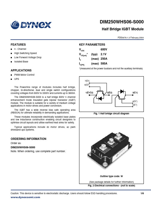
Caution: This device is sensitive to electrostatic discharge. Users should follow ESD handling procedures.1/8KEY PARAMETERS V CES 600V V CE(sat)*(typ)2.1VI C (max)250A I C(PK)(max)500A*(measured at the power busbars and not the auxiliary terminals)FEATURESI n - ChannelI High Switching Speed I Low Forward Voltage Drop IIsolated BaseAPPLICATIONSI PWM Motor Contro l IUPSThe Powerline range of modules includes half bridge,chopper, bi-directional, dual and single switch configurations covering voltages from 600V to 3300V and currents up to 3600A.The DIM250WHS06-S000 is a half bridge 600V n channel enhancement mode insulated gate bipolar transistor (IGBT)module. The module is suitable for a variety of medium voltage applications in motor drives and power conversion.The IGBT has a wide reverse bias safe operating area (RBSOA) for ultimate reliability in demanding applications.These modules incorporate electrically isolated base plates and low inductance construction enabling circuit designers to optimise circuit layouts and utilise earthed heat sinks for safety.Typical applications include dc motor drives, ac pwm drivesand ups systems.ORDERING INFORMATIONOrder as:DIM250WHS06-S000Note: When ordering, use complete part number.Fig. 1 Half bridge circuit diagramFig. 2 Electrical connections - (not to scale)Outline type code: W(See package details for further information)PDS5676-1.3 February 2004DIM250WHS06-S000Half Bridge IGBT ModuleDIM250WHS06-S0002/8Caution: This device is sensitive to electrostatic discharge. Users should follow ESD handling procedures.Test ConditionsV GE = 0V-T case = 65˚C 1ms, T case = 95˚C T case = 25˚C, T j = 150˚C V R = 0, t p = 10ms, T vj = 125˚CCommoned terminals to base plate. AC RMS, 1 min, 50Hz Symbol V CES V GES I C I C(PK)P max I 2t V isolABSOLUTE MAXIMUM RATINGS - PER ARMStresses above those listed under 'Absolute Maximum Ratings' may cause permanent damage to the device. In extreme conditions, as with all semiconductors, this may include potentially hazardous rupture of the package. Appropriate safety precautions should always be followed. Exposure to Absolute Maximum Ratings may affect device reliability.T case = 25˚C unless stated otherwise Units V V A A W kA 2s kVMax.600±202505001157TBD 2.5ParameterCollector-emitter voltage Gate-emitter voltage Continuous collector current Peak collector currentMax. transistor power dissipation Diode I 2t valueIsolation voltage - per moduleSymbol R th(j-c)R th(j-c)R th(c-h)T jT stg -Test ConditionsContinuous dissipation -junction to caseContinuous dissipation -junction to caseMounting torque 5Nm (with mounting grease)Transistor Diode-Mounting - M6Electrical connections - M6ParameterThermal resistance - transistorThermal resistance - diode Thermal resistance - case to heatsink (per module)Junction temperature Storage temperature range Screw torqueUnits ˚C/kW˚C/kW˚C/kW˚C ˚C ˚C Nm NmMax.1082031515012512555Typ.--------Min.-----–4032.5THERMAL AND MECHANICAL RATINGSInternal insulation: Al 2O 3Clearance: 13mmBaseplate material: Cu CTI (Critical Tracking Index): 175Creepage distance: 24mmDIM250WHS06-S000Caution: This device is sensitive to electrostatic discharge. Users should follow ESD handling procedures.3/8Note:†Measured at the power busbars and not the auxiliary terminals.L* is the circuit inductance + L MTest ConditionsV GE = 0V, V CE = V CESV GE = 0V, V CE = V CES , T case = 125˚CV GE = ±20V, V CE = 0V I C = 10mA, V GE = V CE V GE = 15V, I C = 250AV GE = 15V, I C = 250A, , T case = 125˚CDC t p = 1ms I F = 250AI F = 250A, T case = 125˚CV CE = 25V, V GE = 0V, f = 1MHz--ParameterCollector cut-off currentGate leakage current Gate threshold voltageCollector-emitter saturation voltageDiode forward currentDiode maximum forward current Diode forward voltageInput capacitance Module inductanceInternal transistor resistance - per armELECTRICAL CHARACTERISTICST case = 25˚C unless stated otherwise.Symbol I CESI GES V GE(TH)V CE(sat)†I F I FM V F †C ies L M R INTUnits mA mA µA V V V A A V V nF nH m ΩMax.11017.52.62.82505001.81.8--Typ.---5.52.12.3--1.51.527200.23Min.---4.5---------DIM250WHS06-S0004/8Caution: This device is sensitive to electrostatic discharge. Users should follow ESD handling procedures.Units ns ns mJ ns ns mJ µC µC A mJMax.----------Typ.60025020330130122151854Min.----------Test ConditionsI C = 250A V GE = ±15V V CE = 300V R G(ON) = R G(OFF) = 4.7ΩL ~ 100nHI F = 250A, V R = 300V,dI F /dt = 3600A/µs ParameterTurn-off delay time Fall timeTurn-off energy loss Turn-on delay time Rise timeTurn-on energy loss Gate chargeDiode reverse recovery charge Diode reverse currentDiode reverse recovery energyELECTRICAL CHARACTERISTICST case = 25˚C unless stated otherwise Symbol t d(off)t f E OFF t d(on)t r E ON Q g Q rr I rr E RECT case = 125˚C unless stated otherwise Units ns ns mJ ns ns mJ µC A mJMax.---------Typ.6505003040016018232005Min.---------Test ConditionsI C = 250A V GE = ±15V V CE = 300V R G(ON) = R G(OFF) = 4.7ΩL ~ 100nHI F = 250A, V R = 300V,dI F /dt = 3600A/µs ParameterTurn-off delay time Fall timeTurn-off energy loss Turn-on delay time Rise timeTurn-on energy lossDiode reverse recovery charge Diode reverse currentDiode reverse recovery energySymbol t d(off)t f E OFF t d(on)t r E ON Q rr I rr E RECDIM250WHS06-S000Caution: This device is sensitive to electrostatic discharge. Users should follow ESD handling procedures.5/8TYPICAL CHARACTERISTICSFig.3 Typical output characteristicsFig.4 Typical output characteristicsFig.4 Typical switching energy vs collector currentFig.5 Typical switching energy vs gate resistanceDIM250WHS06-S0006/8Caution: This device is sensitive to electrostatic discharge. Users should follow ESD handling procedures.Fig.6 Diode typical forward characteristicsDIM250WHS06-S000PACKAGE DETAILSFor further package information, please visit our website or contact Customer Services. All dimensions in mm, unless stated otherwise. DO NOT SCALE.Fig. 15 Package detailsCaution: This device is sensitive to electrostatic discharge. Users should follow ESD handling procedures.7/8POWER ASSEMBLY CAPABILITYThe Power Assembly group was set up to provide a support service for those customers requiring more than the basicsemiconductor, and has developed a flexible range of heatsink and clamping systems in line with advances in device voltages and current capability of our semiconductors.We offer an extensive range of air and liquid cooled assemblies covering the full range of circuit designs in general use today.The Assembly group offers high quality engineering support dedicated to designing new units to satisfy the growing needs of our customers.Using the latest CAD methods our team of design and applications engineers aim to provide the Power Assembly Complete Solution (PACs).HEATSINKSThe Power Assembly group has its own proprietary range of extruded aluminium heatsinks which have been designed to optimise the performance of Dynex semiconductors. Data with respect to air natural, forced air and liquid cooling (with flow rates) is available on request.For further information on device clamps, heatsinks and assemblies, please contact your nearest sales representative or Customer Services.CUSTOMER SERVICETel: +44 (0)1522 502753 / 502901. Fax: +44 (0)1522 500020SALES OFFICESBenelux, Italy & Switzerland: Tel: +33 (0)1 64 66 42 17. Fax: +33 (0)1 64 66 42 19.France: Tel: +33 (0)2 47 55 75 53. Fax: +33 (0)2 47 55 75 59.Germany, Northern Europe, Spain & Rest Of World: Tel: +44 (0)1522 502753 / 502901.Fax: +44 (0)1522 500020North America: Tel: (440) 259-2060. Fax: (440) 259-2059. Tel: (949) 733-3005. Fax: (949) 733-2986.These offices are supported by Representatives and Distributors in many countries world-wide.© Dynex Semiconductor 2003 TECHNICAL DOCUMENTATION – NOT FOR RESALE. PRODUCED IN UNITED KINGDOMHEADQUARTERS OPERATIONS DYNEX SEMICONDUCTOR LTD Doddington Road, Lincoln.Lincolnshire. LN6 3LF. United Kingdom.Tel: +44-(0)1522-500500Fax: +44-(0)1522-500550This publication is issued to provide information only which (unless agreed by the Company in writing) may not be used, applied or reproduced for any purpose nor form part of any order or contract nor to be regarded as a representation relating to the products or services concerned. No warranty or guarantee express or implied is made regarding the capability, performance or suitability of any product or service. The Company reserves the right to alter without prior notice the specification, design or price of any product or service. Information concerning possible methods of use is provided as a guide only and does not constitute any guarantee that such methods of use will be satisfactory in a specific piece of equipment. It is the user's responsibility to fully determine the performance and suitability of any equipment using such information and to ensure that any publication or data used is up to date and has not been superseded. These products are not suitable for use in any medical products whose failure to perform may result in significant injuryor death to the user. All products and materials are sold and services provided subject to the Company's conditions of sale, which are available on request.All brand names and product names used in this publication are trademarks, registered trademarks or trade names of their respective owners.e-mail:*****************************。
机器视觉英文词汇

机器视觉英文词汇机器视觉英文词汇Aaberration 像差accessory shoes 附件插座、热靴accessory 附件achromatic 消色差的active 主动的、有源的acutance 锐度acute-matte 磨砂毛玻璃adapter 适配器advance system 输片系统ae lock(ael) 自动曝光锁定af illuminatoraf 照明器af spotbeam projectoraf 照明器af(auto focus) 自动聚焦algebraic operation 代数运算一种图像处理运算,包括两幅图像对应像素的和、差、积、商。
aliasing 走样(混叠)当图像象素间距和图像细节相比太大时产生的一种人工痕迹。
alkaline 碱性ambient light 环境光amplification factor 放大倍率analog input/output boards 模拟输入输出板卡analog-to-digital converters 模数转换器ancillary devices 辅助产品angle finder 弯角取景器angle of view 视角anti-red-eye 防红眼aperture priority(ap) 光圈优先aperture 光圈apo(apochromat) 复消色差application-development software 应用开发软件application-specific software 应用软件apz(advanced program zoom) 高级程序变焦arc 弧图的一部分;表示一曲线一段的相连的像素集合。
area ccd solid-state sensors 区域ccd 固体传感器area cmos sensors 区域cmos传感器area-array cameras 面阵相机arrays 阵列asa(american standards association) 美国标准协会asics 专用集成电路astigmatism 像散attached coprocessrs 附加协处理器auto bracket 自动包围auto composition 自动构图auto exposure bracketing 自动包围曝光auto exposure 自动曝光auto film advance 自动进片auto flash 自动闪光auto loading 自动装片auto multi-program 自动多程序auto rewind 自动退片auto wind 自动卷片auto zoom 自动变焦autofocus optics 自动聚焦光学元件automatic exposure(ae) 自动曝光automation/robotics 自动化/机器人技术automation 自动化auxiliary 辅助的Bback light compensation 逆光补偿back light 逆光、背光back 机背background 背景backlighting devices 背光源backplanes 底板balance contrast 反差平衡bar code system 条形码系统barcode scanners 条形码扫描仪barrel distortion 桶形畸变base-stored image sensor (basis) 基存储影像传感器battery check 电池检测battery holder 电池手柄bayonet 卡口beam profilers 电子束仿形器beam splitters 光分路器bellows 皮腔binary image 二值图像只有两级灰度的数字图像(通常为0和1,黑和白)biometrics systems 生物测量系统blue filter 蓝色滤光镜blur 模糊由于散焦、低通滤波、摄像机运动等引起的图像清晰度的下降。
Infineon 2EDF7275双向图腾柱PFC

Infineon 2EDF7275F 3300W CCM双向图腾柱PFC解决方案infineon公司的EiceDRIVER™ 2Edi系列产品是双路隔离MOSFET栅极驱动器,通过无芯变压器(CT)技术提供功能(2EDFx)或增强(2EDSx)输入/输出隔离.由于具有高驱动电流,极好的共模抑制和快速信号传输,2EDi 系列特别适用于驱动快速开关电源系统的中压到高压MOSFET (CoolMOS™, OptiMOS™, CoolSIC™).源/沉输出电流为4A/8A或1A/2A,高达10MHz PWM开关频率,PWM信奉传输时延典型值为37ns:通路到通路不匹配为3ns,传输时延变化为+7/-6ns.电阻可编程死区控制(DTC)范围从15ns到250ns.共模瞬态免疫度CMTI大于150V/ns,输入边欠压锁住(UVLO)情况下快速安全关断,4V或8V UVLO阈值输出电压从4.5V到20V,工作温度TJ = -40C 到+150C.主要用在服务器,通信和工业SMPS,同步整流,砖型转换器,UPS和电池存储,以EV充电工业自动化,马达驱动和电动工具.本文介绍了2EDF7275F主要特性,框图,应用电路,以及3300W CCM双向图腾柱评估板EVAL_3K3W_TP_PFC_SIC主要特性,主板和控制板电路图.The EiceDRIVER™ 2EDi is a family of fast dual-channel isolated MOSFET gate-driver ICs providing functional (2EDFx) or reinforced (2EDSx) input-to-output isolation by means of coreless transformer (CT) technology. Due to high driving current, excellent common-mode rejection and fast signal propagation,2EDi is particularly well suited for driving medium- to high-voltage MOSFETs (CoolMOS™, OptiMOS™, CoolSIC™) in fast-switching power systems.The ga te drivers of the EiceDRIVER™ 2EDi product family are designed for fast-switching, medium to high power systems with MOSFET switches. They are optimized for high timing accuracy over temperature and production spread. The reliable accurate timing simp lifi es system design and provides better power conversion efficiency.The 2EDSx, 2EDFx dual-channel reinforced (safe) and functional isolated product variants are available with different drive strengths: 4 A/8 A for low-ohmic power MOSFETs, 1 A/2 A for higher Ron MOSFETs or slower switching transients (EMI). The 1 A/2 A reinforced isolation driver can also be used as a PWM Data Coupler in combination with a non-isolated boost gate driver such as 1EDNx 4 A/8 A placed in closest proximity to the Superjunction power switches.Two independent and galvanically isolated gate driver channels ensure that all 2EDi versions can be used in any possible configuration of low- and high-side switches.Improved system robustness is supported by min. 150 V/ns Common Mode Transient Immunity (CMTI), PWM inputs with 18 ns noise filter, UVLO on output side including a safety self-lock-down of driver outputs in case of input UVLO (VDDI < 3 V), PWM outputs with up to 5 A peak reverse current capability and an intrinsically robust gate driver design.2EDF7275F主要特性:• 4 A / 8 A or 1 A / 2 A source / sink output current• Up to 10 MHz PWM switching frequency• PWM signal propagation delay typ. 37 ns with– 3 ns channel-to-channel mismatch– +7/-6 ns propagation delay variance• Res istor-programmable Dead Time Control (DTC) ranging from 15 ns to 250 ns• Common Mode Transient Immunity CMTI >150 V/ns• Fast safety turn-off in case of input side Undervoltage Lockout (UVLO)• Output supply voltage from 4.5 V to 20 V with 4 V or 8 V UVLO threshold• Wide temperature operating range TJ = -40C to +150C• RoHS compliant wide /narrow-body (WB/NB) DSO16 and 5mm x 5mm LGA packages• Fully qualified according to JEDEC for Industrial ApplicationsIsolation and safety certificates• 2EDSx with reinforced isolation:– DIN V VDE V 0884-10 (2006-12) compliant with VIOTM = 8 kVpk and VIOSM = 6.25 kVpk (tested at 10kVpk)– certified according to UL1577 (Ed. 5) opto-coupler component isolation standard with VISO = 5700 VRMS– certified according to DIN EN 62368-1 and DIN EN 60950-1 and corresponding CQC certificates– certified according to EN 61010-1 (reinforced isolation, 300 Vrms mains voltage, overvoltage category III)• 2EDFx with functional isolation: Production test with 1.5 kVDC for 10 msEice DRIVER™ 2Edi系列应用:• Server, telecom and industrial SMPS• Synchronous rectification, brick converters, UPS and battery storage• EV charging industry automation, motor drives and power tools图1. 2EDF7275F应用电路(1):5V控制器和自举高边VDDA图2. EiceDRIVER™ 2EDi产品系列框图评估板EVAL_3K3W_TP_PFC_SIC:3300W CCM双向图腾柱和650V CoolSiC™与XMC™The EVAL_3K3W_TP_PFC_SIC board is a system solution enabled by Infineon Technologies power semicon ductors as well as drivers and microcontroller. The evaluation board consists of a bridgeless totem-pole topology and it is intended for high-end applications in which the highest efficiency is required. Furthermore, the totem-pole topology is simple and offers a reduced part count and full utilization of the PFC inductor and switches [1]. For these reasons, totem-pole PFC enables high power density at a limited system cost for high-performance systems. In addition, the EVAL_3K3W_TP_PFC_SIC board provides reverse power flow (inverter operation for grid-connected applications) due to the inherentbi-directional power flow capability of the totem-pole topology.The totem-pole topology in PFC applications with CCM operation is feasible by using wide band-gap semiconductors [1]. In this case, the Infineon CoolSiC™ MOSFET in TO-247 four-pin package is used to push the efficiency to 99 percent at half-load (Figure 2). The converter operates exclusively at high-line (176 Vrms minimum, 230 Vrms nominal) in CCM with 65 kHz switching frequency.This document presents a system solution based on Infineon superjunction (SJ) (CoolMOS™) and wide band-gap (CoolSiC™) power semiconductors, drivers and microcontroller for a bridgeless totem-pole Power Factor Corrector (PFC) with bi-directional capability. The EVAL_3K3W_TP_PFC_SIC board is intended for those applications which require the highest efficiency (99 percent) and high power density (73 W/in3), such as high-end servers and telecoms. In addition, the bi-directional power flow capability would allow this design to be used in battery chargers or battery formation applications. The totem pole implemented in the EVAL_3K3W_TP_PFC_SIC board operates in Continuous Conduction Mode (CCM) in both rectifier (PFC) and inverter mode, with full digital control implementation on the Infineon XMC™ 1000 series microcontroller.The Infineon components used in the 3300 W bridgeless bi-directional totem-pole board are as follows: · 600 V CoolMOS™ C7 SJ MOSFET and 650 V CoolSiC™ silicon carbide MOSFET· 2EDF7275F isolated gate drivers (EiceDRIVER™)· XMC1404 microcontroller· ICE5QSAG CoolSET™ QR Flyback controller· 950 V CoolMOS™ P7 SJ MOSFETThe PFC function to achieve bulk voltage regulation while demanding high-quality current from the grid is implemented with an Infineon XMC1404 microcontroller [2]. Further detail on PFC control implementation in the XMC™ 1000 family can be found in the application notes of other Infineon PSU and PFC evaluation boards with classic boost or dual boost topologies [3][4][5].The 3300 W bridgeless bi-directional (PFC/AC-DC and inverter/AC-DC) totem-pole presented in this application note is a system solution developed with Infineon power semiconductors as well as Infineon drivers and controllers. The Infineon devices used in the implementation of theEVAL_3K3W_TP_PFC_SIC board are listed below.· 64 mΩ 650 V CoolSiC™ (IMZA65R048M1) in TO-247 four-pin package, as totem-pole PFChigh-frequency switches· 17 mΩ 600 V CoolMOS™ C7 (IPW60R017C7) in TO-247 package, for the totem-pole PFC return path (low-frequency bridge)· 2EDF7275F isolated gate drivers (EiceDRIVER™)· ICE5QSAG QR Flyback controller and 950 V CoolMOS™ P7 (IPU95R3K7P7) for the bias auxil iar y supply· XMC1404 microcontroller for PFC control implementationA simplified block diagram of the bridgeless topology with the mentioned devices from the Infineon portfolio is shown in Figure 3. The diode bridge in front of the totem-pole PFC converter is meant to be a current path for start-up or surge conditions and it is not part of the current path during the steady-state converter operation. The power flow direction, which will select the converter operation – forward power flow or PFC operation versus reverse power flow or inverter operation – can be selected by a switch connected to the XMC™ microcontroller as a digital input pin.图3. 评估板EVAL_3K3W_TP_PFC_SIC外形图图4. 评估板EVAL_3K3W_TP_PFC_SIC简化框图图5. 评估板EVAL_3K3W_TP_PFC_SIC不同部分位置图图6. 评估板EVAL_3K3W_TP_PFC_SIC主板电路图图7. 评估板EVAL_3K3W_TP_PFC_SIC控制板电路图。
Infineon 2EDF7275F驱动器解决方案

Infineon 2EDF7275F双路隔离MOSFET栅极驱动器解决方案infineon公司的EiceDRIVER™2EDF7275F是双路隔离MOSFET栅极驱动器集成电路系列,通过无芯变压器(CT)技术,提供功能(2EDFx)或加强(2EDSx)输入/输出隔离性能.由于高驱动电流,极好的共模抑制和快速信号传输,2EDi系列特别适合于开速开关电源系统中驱动中/高压MOSFET器件(CoolMOS™, OptiMOS™, CoolSIC™).2EDSx, 2EDFx双路加强(安全)和功能隔离产品有不同的驱动强度:4A/8A低欧姆功率MOSFET,1A/2A高Ron MOSFET或更低开关瞬态(EMI).器件提供4A/8A或1A/2A源/沉输出电流,高达10MHz PWM开关频率,PWM信号传输时延0.37ns:通路不匹配3ns和+7/-6 ns传播延迟方差.输出电源电压从4.5V到20V,工作温度TJ = -40℃到+150℃.主要用在服务器,通信和工业开关电源(SMPS),同步整流,砖型转换器,UPS和电池存储,EV充电工业自动化,马达驱动和电动工具.为您整理如下详细资料,本文介绍了2EDF7275F主要特性,2EDi系列框图,以及评估板EVAL_3K3W_TP_PFC_SIC主要特性,指标.The EiceDRIVER™ 2EDi is a family of fast dual-channel isolated MOSFET gate-driver ICs providing functional(2EDFx) or reinforced (2EDSx) input-to-output isolation by means of coreless transformer (CT) technology. Dueto high driving current, excellent common-mode rejection and fast signal propagation,2EDi is particularly wellsuited for driving medium- to high-voltage MOSFETs (CoolMOS™, OptiMOS™, CoolSIC™) in fast-switching power systems.The gate drivers of the EiceDRIVER™ 2EDi product family are designed for fast-switching, medium to high powersystems with MOSFET switches. They are optimized for high timing accuracy over temperature and productionspread. The reliable accurate timing simp lifi es system design and provides better power conversion efficiency.The 2EDSx, 2EDFx dual-channel reinforced (safe) and functional isolated product variants are available withdifferent drive strengths: 4 A/8 A for low-ohmic power MOSFETs, 1 A/2 A for higher Ron MOSFETs or slowerswitching transients (EMI). The 1 A/2 A reinforced isolation driver can also be used as a PWM Data Coupler incombination with a non-isolated boost gate driver such as 1EDNx 4 A/8 A placed in closest proximity to theSuperjunction power switches.Two independent and galvanically isolated gate driver channels ensure that all 2EDi versions can be used in anypossible configuration of low- and high-side switches.Improved system robustness is supported by min. 150 V/ns Common Mode Transient Immunity (CMTI), PWMinputs with 18 ns noise filter, UVLO on output side including a safety self-lock-down of driver outputs in case ofinput UVLO (VDDI < 3 V), PWM outputs with up to 5 A peak reverse current capability and an intrinsically robustgate driver design.The 2EDi product table is provided as a first quick device selection guide; more detailed specifications areprovided in the product features, package dimension and testing chapters of this datasheet.2EDF7275F主要特性:• 4 A/8 A or 1 A/2 A source/sink output current• Up to 10 MHz PWM switching frequency• PWM signal propagation delay typ. 37 ns with– 3 ns channel-to-channel mismatch– +7/-6 ns propagation delay variance• Resistor-programmable Dead Time Control (DTC) ranging from 15 ns to 250 ns• Common Mode Transient Immunity CMTI >150 V/ns• Fast safety turn-off in case of input side Undervoltage Lockout (UVLO)• Output supply voltage from 4.5 V to 20 V with 4 V or 8 V UVLO threshold• Wide temperature operating range TJ = -40°C to +150°C• RoHS compliant wide /narrow-body (WB/NB) DSO16 and 5mm x 5mm LGA packages• Fully qualified according to JEDEC for Industrial ApplicationsIsolation and safety certificates• 2EDSx with reinforced isolation:– DIN V VDE V 0884-10 (2006-12) compliant with VIOTM = 8 kVpk and VIOSM = 6.25 kVpk (tested at 10kVpk)– certified according to UL1577 (Ed. 5) opto-coupler component isolation standard with VISO = 5700 VRMS– certified according to DIN EN 62368-1 and DIN EN 60950-1 and corresponding CQC certificates– certified according to EN 61010-1 (reinforced isolation, 300 Vrms mains voltage, overvoltage category III)• 2EDFx with functional isolation: Production test with 1.5 kVDC for 10 ms2EDF7275F潜在应用:• Server, telecom and industrial SMPS• Synchronous r ectification, brick converters, UPS and battery storage• EV charging industry automation, motor drives and power tools图1.EiceDRIVER™ 2EDi系列框图图2.EiceDRIVER™ 2EDi系列和5V控制器和高边VDD自举的应用电路评估板EVAL_3K3W_TP_PFC_SICThe EVAL_3K3W_TP_PFC_SIC board is a system solution enabled by Infineon Technologiespower semicon ductors as well as drivers and microcontroller. The evaluation board consists of a bridgeless totem-pole topology and it is intended for high-end applications in which the highest efficiency is required. Furthermore, the totem-pole topology is simple and offers a reduced part count and full utilization of the PFC inductor and switches [1]. For these reasons, totem-pole PFC enables high power density at a limited system cost for high-performance systems. In addition, theEVAL_3K3W_TP_PFC_SIC board provides reverse power flow (inverter operation for grid-connected applications) due to the inherent bi-directional power flow capability of the totem-pole topology.The totem-pole topology in PFC applications with CCM operation is feasible by using wide band-gap semiconductors [1]. In this case, the Infineon CoolSiC™ MOSFET in TO-247 four-pin package is used to push the efficiency to 99 percent at half-load (Figure 2). The converter operates exclusively at high-line (176 Vrms minimum, 230 Vrms nominal) in CCM with 65 kHz switching frequency.The PFC function to achieve bulk voltage regulation while demanding high-quality current from the grid is implemented with an Infineon XMC1404 microcontroller [2]. Further detail on PFC control implementation in the XMC™ 1000 family can be found in the application notes of other Infineon PSU and PFC evaluation boards with classic boost or dual boost topologies [3][4][5].The 3300 W bridgeless bi-directional (PFC/AC-DC and inverter/AC-DC) totem-pole presented in thisapplication note is a system solution developed with Infineon power semiconductors as well as Infineon drivers and controllers. The Infineon devices used in the implementation of theEVAL_3K3W_TP_PFC_SIC board are listed below.64 mΩ 650 V CoolSiC™ (IMZA65R048M1) in TO-247 four-pin package, as totem-pole PFChigh-frequency switches17 mΩ 600 V CoolMOS™ C7 (IPW60R017C7) in TO-247 package, for the totem-pole PFC return path (low-frequency bridge)2EDF7275F isolated gate drivers (EiceDRIVER™)ICE5QSAG QR Flyback controller and 950 V CoolMOS™ P7 (IPU95R3K7P7) for the bias auxil iar y supplyXMC1404 microcontroller for PFC control implementationA simplified block diagram of the bridgeless topology with the mentioned devices from the Infineon portfolio is shown in Figure 3. The diode bridge in front of the totem-pole PFC converter is meant to be a current path for start-up or surge conditions and it is not part of the current path during the steady-state converter operation. The power flow direction, which will select the converter operation – forward power flow or PFC operation versus reverse power flow or inverter operation – can be selected by a switch connected to the XMC™ microcontroller as a digital input pin.This document presents a system solution based on Infineon superjunction (SJ) (CoolMOS™) and wide band-gap (CoolSiC™) power semiconductors, drivers and microcontroller for a bridgeless totem-pole Power Factor Corrector (PFC) with bi-directional capability. The EVAL_3K3W_TP_PFC_SIC board is intended for those applications which require the highest efficiency (99 percent) and high power density (73 W/in3), such as high-end servers and telecoms. In addition, the bi-directional power flow capability would allow this design to be used in battery chargers or battery formation applications. The totem pole implemented in the EVAL_3K3W_TP_PFC_SIC board operates in Continuous Conduction Mode (CCM) in both rectifier (PFC) and inverter mode, with full digital control implementation on the Infineon XMC™ 1000 series microcontroller.The Infineon components used in the 3300 W bridgeless bi-directional totem-pole board are as follows:600 V CoolMOS™ C7 SJ MOSFET and 650 V CoolSiC™ silicon carbide MOSFET2EDF7275F isolated gate drivers (EiceDRIVER™)XMC1404 microcontrollerICE5QSAG CoolSET™ QR Flyback controller950 V CoolMOS™ P7 SJ MOSFET图3.3300W无桥图腾柱PFC和CoolSiC™, CoolMOS™ and XMC™控制板评估板EVAL_3K3W_TP_PFC_SIC主要特性:High efficiency bridgeless totem-pole PFCHigh power densityEnabled by CoolSiC™ MOSFET 650VDigitally controlled with XMC1404Bidirectional capability (DC-AC operation)BenefitsEfficiency close to 99%Compact form factor (72W/in3)Low component countBidirectional operation (digital control)图4.3300W无桥图腾柱PFC板(EVAL_3K3W_TP_PFC_SIC)简化框图图5.3300W无桥图腾柱PFC板和650V CoolSiC和600V C7 C OS MOSFET和XMC控制位置图。
Lenovo ThinkSystem DM3000H 统一混合存储阵列产品指南说明书
Lenovo ThinkSystem DM3000H Unified Hybrid Storage ArrayProduct GuideLenovo ThinkSystem DM3000H is a unified, hybrid storage system that is designed to provide performance, simplicity, capacity, security, and high availability for small enterprises and remote offices/branch offices of large enterprises. Powered by the ONTAP software, ThinkSystem DM3000H delivers enterprise-class storage management capabilities with a wide choice of host connectivity options, flexible drive configurations, and enhanced data management features.The ThinkSystem DM3000H is a perfect fit for small offices and remote and branch offices of large enterprises that run a wide range of general purpose workloads, including file services, virtualization, Microsoft applications, backup and archiving, and other storage I/O-intensive applications.ThinkSystem DM3000H models are 2U rack-mount controller enclosures that include two controllers, 64 GB RAM and 8 GB battery-backed NVRAM per system (32 GB RAM and 4 GB NVMRAM per controller), and12 LFF hot-swap drive bays (2U12 form factor). Controllers provide universal 1/10 GbE NAS/iSCSI or4/8/16 Gb Fibre Channel (FC) ports, or 1/10 GbE RJ-45 ports for host connectivity.A single ThinkSystem DM3000H Storage Array scales up to 144 drives with the attachment of ThinkSystemDM120S 2U12 LFF, DM600S 4U60 LFF, and DM240S 2U24 SFF Expansion Enclosures.Figure 1. Lenovo ThinkSystem DM3000HUp to 12 DM3000H Storage Arrays can be combined into a clustered system in a NAS environment, or up to6 DM3000H Storage Arrays can be combined into a clustered system in a SAN environment.Did you know?A single ThinkSystem DM3000H can scale up to 2.3 PB of raw storage capacity. A cluster of the DM3000H storage arrays can scale up to 27.6 PB for NAS or up to 13.8 PB for SAN environments.The ThinkSystem DM3000H offers unified file and block storage connectivity with support for 1 GbE or 10 GbE NAS and iSCSI, and 8 Gb or 16 Gb Fibre Channel protocols at the same time.Click here to check for updatesFigure 2. ThinkSystem DM3000H or DM120S 2U12 LFF enclosure front viewThe front of the DM3000H or DM120S 2U LFF enclosure includes the following components:12 LFF hot-swap drive baysEnclosure status LEDsEnclosure ID LEDThe following figure shows the rear of the ThinkSystem DM3000H 2U controller enclosure with universal SFP+ host ports.Figure 3. ThinkSystem DM3000H 2U controller enclosure rear view: Universal SFP+ host portsThe following figure shows the rear of the ThinkSystem DM3000H 2U controller enclosure with 10GBASE-T host ports.Figure 4. ThinkSystem DM3000H 2U controller enclosure rear view: 10GBASE-T host portsFigure 5. ThinkSystem DM240S expansion enclosure front viewThe front of the ThinkSystem DM240S 2U SFF expansion enclosure includes the following components:24 SFF hot-swap drive baysEnclosure status LEDsEnclosure ID LEDThe following figure shows the rear of the DM120S and DM240S 2U expansion enclosure.Figure 6. ThinkSystem DM120S or DM240S 2U expansion enclosure rear viewFigure 7. ThinkSystem DM600S 4U LFF expansion enclosure front viewThe front of the ThinkSystem DM600S 4U LFF expansion enclosure includes the following components: Five drawers, each with 12 LFF hot-swap drive bays.Enclosure status LEDs.Enclosure ID LED.Figure 8. ThinkSystem DM600S 4U LFF expansion enclosure rear viewThe rear of the ThinkSystem DM600S 4U LFF expansion enclosure includes the following components: Two redundant hot-swap I/O Modules; each I/O Module provides four 12 Gb SAS x4 expansion ports (Mini-SAS HD SFF-8644) for connections to the controller enclosures and for connecting the expansion enclosures between each other.Two redundant hot-swap 2325 W (200 - 240 V) AC power supplies (IEC 320-C20 power connector) Two hot-swap cooling fan modules; each module has two fans.Note: The failed cooling module should be replaced as soon as possible.I/O Module status LEDs.System specificationsThe following table lists the ThinkSystem DM3000H storage system specifications.Lenovo 15m LC-LC OM4 MMF Cable 4Z57A10850B2PE 12Lenovo 25m LC-LC OM4 MMF Cable 4Z57A10851B2PF 12Lenovo 30m LC-LC OM4 MMF Cable 4Z57A10852B2PG 12OM3 cable options for 8 Gb FC, 16 Gb FC, and 10 GbE SW SFP+ optical transceiversLenovo 0.5m LC-LC OM3 MMF Cable 00MN499ASR512Lenovo 1m LC-LC OM3 MMF Cable 00MN502ASR612Lenovo 3m LC-LC OM3 MMF Cable 00MN505ASR712Lenovo 5m LC-LC OM3 MMF Cable 00MN508ASR812Lenovo 10m LC-LC OM3 MMF Cable 00MN511ASR912Lenovo 15m LC-LC OM3 MMF Cable 00MN514ASRA 12Lenovo 25m LC-LC OM3 MMF Cable 00MN517ASRB 12Lenovo 30m LC-LC OM3 MMF Cable 00MN520ASRC 12DAC cable options for 10 GbE SFP+ connectivity (SFP+ base, adapter card, and interconnect ports)0.5m Passive DAC SFP+ Cable 00D6288A3RG 121m Passive DAC SFP+ Cable 90Y9427A1PH 121.5m Passive DAC SFP+ Cable 00AY764A51N 122m Passive DAC SFP+ Cable 00AY765A51P 123m Passive DAC SFP+ Cable 90Y9430A1PJ 125m Passive DAC SFP+ Cable 90Y9433A1PK 127m Passive DAC SFP+ Cable 00D6151A3RH 12UTP Category 6 cables options for 1/10 GbE RJ-45 host connectivity and 1 GbE RJ-45 management ports0.75m Green Cat6 Cable 00WE123AVFW 101.0m Green Cat6 Cable 00WE127AVFX 101.25m Green Cat6 Cable 00WE131AVFY 101.5m Green Cat6 Cable 00WE135AVFZ 103m Green Cat6 Cable 00WE139AVG01010m Green Cat6 Cable 90Y3718A1MT 1025m Green Cat6 Cable90Y3727A1MW10DescriptionPart number Featurecode Maximum quantity per controller enclosure * Factory-installed only.Figure 9. DM3000H expansion enclosure connectivity topologyExpansion cabling rules:Port 0b on the Controller 1 is the primary path that is connected to the Port 3 on the I/O Module A in the last expansion enclosure in a stack.Port 1 on the I/O Module A in the last expansion enclosure is connected to Port 3 on the I/O Module A in the adjacent expansion enclosure, and so on (until the first expansion enclosure in a stack is cabled).Port 0a on the Controller 1 is the secondary path that is connected to the Port 1 on the I/O Module B in the first expansion enclosure in a stack.Port 0b on the Controller 2 is the primary path that is connected to the Port 3 on the I/O Module B in the last expansion enclosure in a stack.96TB (6x 16TB NL SAS HDDs) 2U12 Drive Pack for DM3000H - Fundamentals4XB7A65399BCV62DescriptionPart number Feature code Maximum quantityper 2U12enclosure The following table lists supported drive packs for the DM600S 4U60 LFF expansion enclosures.Table 10. DM600S 4U60 LFF drive packs for ONTAPDescriptionPart number Feature code Maximumquantityper 4U60enclosure 3.5-inch 12 Gbps NL SAS hot-swap HDDsThinkSystem 120TB (30x 4TB NL SAS HDDs) 4U60 Drive Pack for DM3000H 4XB7A14684B3X32ThinkSystem 240TB (30x 8TB NL SAS HDDs) 4U60 Drive Pack for DM3000H 4XB7A14685B3WZ 2ThinkSystem 300TB (30x 10TB NL SAS HDDs) 4U60 Drive Pack for DM3000H 4XB7A14686B3X12ThinkSystem 480TB (30x 16TB NL SAS HDDs) 4U60 Drive Pack for DM3000H4XB7A65405BCVC2Table 11. DM600S 4U60 LFF drive packs for ONTAP FundamentalsDescriptionPart number Feature code Maximumquantityper 4U60enclosure 3.5-inch 12 Gbps NL SAS hot-swap HDDs120TB (30x 4TB NL SAS HDDs) 4U60 Drive Pack for DM3000H - Fundamentals 4XB7A39389B73Q 2240TB (30x 8TB NL SAS HDDs) 4U60 Drive Pack for DM3000H - Fundamentals4XB7A39390B73R2300TB (30x 10TB NL SAS HDDs) 4U60 Drive Pack for DM3000H - Fundamentals 4XB7A39391B73S 2480TB (30x 16TB NL SAS HDDs) 4U60 Drive Pack for DM3000H - Fundamentals 4XB7A65404BCVB2The following table lists supported drive packs for the DM240S 2U24 SFF expansion enclosures.Table 12. DM240S 2U24 SFF drive packs for ONTAPDescriptionPart number Feature code Maximumquantityper 2U24enclosure 2.5-inch 12 Gbps SAS hot-swap SSDs (1 Drive Write per Day)ThinkSystem 5.76TB (6x 960GB SAS SSDs) 2U24 Drive Pack for DM3000H 4XB7A16999B6774ThinkSystem 23.04TB (6x 3.84TB SAS SSDs) 2U24 Drive Pack for DM3000H 4XB7A17001B6794ThinkSystem 46.08TB (6x 7.68TB SAS SSDs) 2U24 Drive Pack for DM3000H 4XB7A17003B67B 4ThinkSystem 92.16TB (6x 15.36TB SAS SSDs) 2U24 Drive Pack for DM3000H 4XB7A17005B67D 42.5-inch 12 Gbps SAS hot-swap HDDsThinkSystem 5.4TB (6x 900GB SAS 10K HDDs) 2U24 Drive Pack for DM3000H 4XB7A17007B67F 4ThinkSystem 7.2TB (6x 1.2TB SAS 10K HDDs) 2U24 Drive Pack for DM3000H 4XB7A17009B67H 4ThinkSystem 10.8TB (6x 1.8TB SAS 10K HDDs) 2U24 Drive Pack for DM3000H4XB7A17011B67K4Table 15. Software selectionFeaturecode Description Availability ONTAP 9.11BRK0Lenovo ThinkSystem DM Series ONTAP 9.11 Software Base NonEncryption China only BRJW Lenovo ThinkSystem DM Series ONTAP 9.11 Software Encryption All markets exceptChinaBRJX Lenovo ThinkSystem DM Series ONTAP 9.11 Software NonEncryption All marketsBRJY Lenovo ThinkSystem DM Series ONTAP 9.11 Software Fundamentals Encryption All markets exceptChinaBRJZ Lenovo ThinkSystem DM Series ONTAP 9.11 Software FundamentalsNonEncryptionAll markets ONTAP 9.12BU6N Lenovo ThinkSystem DM Series ONTAP 9.12 Software Base NonEncryption China onlyBU6Q Lenovo ThinkSystem DM Series ONTAP 9.12 Software Fundamentals Encryption All markets exceptChinaBU6P Lenovo ThinkSystem DM Series ONTAP 9.12 Software Fundamentals NonEncryption All markets except ChinaBU6S Lenovo ThinkSystem DM Series ONTAP 9.12 Software Encryption All markets exceptChinaBU6R Lenovo ThinkSystem DM Series ONTAP 9.12 Software NonEncryption All markets exceptChinaSoftware maintenance is included in the DM3000H warranty and support (see Warranty and support for details).Extended ONTAP featuresFabricPool and SnapLock WORM data protection are optional extended features. To obtain these feature licenses, order the part numbers as listed in the following table. Upgrades are supported in specific bundles as listed in the Comparison of software features table.Note: Extended features are only available as field upgrades and are not orderable as part of a CTO configuration.Table 16. Optional software featuresPart number Feature code Description Quantity4P47A16547None*DM Series SnapLock License 1 per system (contains two licenses) 4P47A37057None*DM Series FabricPool – 1TB Increment – 3 years 1 per TB of storage capacity4P47A37288None*DM Series FabricPool – 1TB Increment – 5 years 1 per TB of storage capacity4P47A82668BPQ6Security and Compliance Bundle 1 per system (contains two licenses) 4P47A83121BQ8X Hybrid Cloud Bundle 3 year per TB License 1 per TB of storage capacity4P47A83123BQ8W Hybrid Cloud Bundle 5 year per TB License 1 per TB of storage capacity* Field upgrade only; no factory installation.The ThinkSystem DM600S 4U60 LFF expansion enclosures ship with two redundant hot-swap 2325 W (200 -240 V) Platinum AC power supplies, each with an IEC 320-C20 connector.Each ThinkSystem DM Series enclosure requires the selection of two power cables.The following table lists the rack power cable and line cord options that can be ordered for the DM3000H, DM120S 2U12 LFF, and DM240S 2U24 SFF enclosures (two power cords per enclosure).Table 18. Power cables for DM3000H, DM120S 2U12 LFF, and DM240S 2U24 SFF enclosuresDescription PartnumberFeaturecodeRack power cables1.0m, 10A/100-250V, C13 to IEC 320-C14 Rack Power Cable00Y3043A4VP 1.0m, 13A/100-250V, C13 to IEC 320-C14 Rack Power Cable4L67A08367B0N5 1.2m, 16A/100-250V, 2 Short C13s to Short C20 Rack Power Cable47C2491A3SW 1.5m, 10A/100-250V, C13 to IEC 320-C14 Rack Power Cable39Y793762011.5m, 13A/100-250V, C13 to IEC 320-C14 Rack Power Cable4L67A08368B0N62.0m, 10A/100-250V, C13 to IEC 320-C14 Rack Power Cable4L67A08365B0N4 2.0m, 13A/125V-10A/250V, C13 to IEC 320-C14 Rack Power Cable4L67A083696570 2.5m, 16A/100-250V, 2 Long C13s to Short C20 Rack Power Cable47C2492A3SX 2.8m, 10A/100-250V, C13 to IEC 320-C14 Rack Power Cable4L67A083666311 2.8m, 13A/125V-10A/250V, C13 to IEC 320-C14 Rack Power Cable4L67A083706400 2.8m, 10A/100-250V, C13 to IEC 320-C20 Rack Power Cable39Y79386204 2.8m, 16A/100-250V, 2 Short C13s to Long C20 Rack Power Cable47C2493A3SY 4.1m, 16A/100-250V, 2 Long C13s to Long C20 Rack Power Cable47C2494A3SZ 4.3m, 10A/100-250V, C13 to IEC 320-C14 Rack Power Cable39Y79326263 4.3m, 13A/125V-10A/250V, C13 to IEC 320-C14 Rack Power Cable4L67A083716583 Line cordsArgentina 2.8m, 10A/250V, C13 to IRAM 2073 Line Cord39Y79306222 Argentina 4.3m, 10A/250V, C13 to IRAM 2073 Line Cord81Y23846492 Australia/New Zealand 2.8m, 10A/250V, C13 to AS/NZS 3112 Line Cord39Y79246211 Australia/New Zealand 4.3m, 10A/250V, C13 to AS/NZS 3112 Line Cord81Y23836574 Brazil 2.8m, 10A/250V, C13 to NBR 14136 Line Cord69Y19886532 Brazil 4.3m, 10A/250V, C13 to NBR14136 Line Cord81Y23876404 China 2.8m, 10A/250V, C13 to GB 2099.1 Line Cord39Y79286210 China 4.3m, 10A/250V, C13 to GB 2099.1 Line Cord81Y23786580 Denmark 2.8m, 10A/250V, C13 to DK2-5a Line Cord39Y79186213 Denmark 4.3m, 10A/250V, C13 to DK2-5a Line Cord81Y23826575 Europe 2.8m, 10A/250V, C13 to CEE7-VII Line Cord39Y79176212 Europe 4.3m, 10A/250V, C13 to CEE7-VII Line Cord81Y23766572 India 2.8m, 10A/250V, C13 to IS 6538 Line Cord39Y79276269 India 4.3m, 10A/250V, C13 to IS 6538 Line Cord81Y23866567 Israel 2.8m, 10A/250V, C13 to SI 32 Line Cord39Y79206218 Israel 4.3m, 10A/250V, C13 to SI 32 Line Cord81Y23816579 Italy 2.8m, 10A/250V, C13 to CEI 23-16 Line Cord39Y79216217 Italy 4.3m, 10A/250V, C13 to CEI 23-16 Line Cord81Y23806493Japan 2.8m, 12A/125V, C13 to JIS C-8303 Line cord46M2593A1RE Japan 2.8m, 12A/250V, C13 to JIS C-8303 Line Cord4L67A083576533 Japan 4.3m, 12A/125V, C13 to JIS C-8303 Line Cord39Y79266335 Japan 4.3m, 12A/250V, C13 to JIS C-8303 Line Cord4L67A083626495 Korea 2.8m, 12A/250V, C13 to KS C8305 Line Cord39Y79256219 Korea 4.3m, 12A/250V, C13 to KS C8305 Line Cord81Y23856494 South Africa 2.8m, 10A/250V, C13 to SABS 164 Line Cord39Y79226214 South Africa 4.3m, 10A/250V, C13 to SABS 164 Line Cord81Y23796576 Switzerland 2.8m, 10A/250V, C13 to SEV 1011-S24507 Line Cord39Y79196216 Switzerland 4.3m, 10A/250V, C13 to SEV 1011-S24507 Line Cord81Y23906578 Taiwan 2.8m, 10A/250V, C13 to CNS 10917-3 Line Cord81Y23756317 Taiwan 2.8m, 15A/125V, C13 to CNS 10917-3 Line Cord81Y23746402 Taiwan 4.3m, 10A/250V, C13 to CNS 10917-3 Line Cord81Y23896531 Taiwan 4.3m, 15A/125V, C13 to CNS 10917-3 Line Cord81Y23886530 United Kingdom 2.8m, 10A/250V, C13 to BS 1363/A Line Cord39Y79236215 United Kingdom 4.3m, 10A/250V, C13 to BS 1363/A Line Cord81Y23776577 United States 2.8m, 10A/125V, C13 to NEMA 5-15P Line Cord90Y30166313 United States 2.8m, 10A/250V, C13 to NEMA 6-15P Line Cord46M2592A1RF United States 2.8m, 13A/125V, C13 to NEMA 5-15P Line Cord00WH5456401 United States 4.3m, 10A/125V, C13 to NEMA 5-15P Line Cord4L67A083596370 United States 4.3m, 10A/250V, C13 to NEMA 6-15P Line Cord4L67A083616373 United States 4.3m, 13A/125V, C13 to NEMA 5-15P Line Cord4L67A08360AX8A Description number code The following table lists the rack power cable and line cord options that can be ordered for the DM600S 4U60 LFF expansion enclosures (two power cords per enclosure).Table 19. Power cables for DM600S 4U60 enclosuresDescription PartnumberFeaturecodeRack power cables2.5m, 16A/100-250V, C19 to IEC 320-C20 Rack Power Cable39Y79166252 Line cordsArgentina 4.3m, 16A/250V, C19 to IRAM 2073 Line Cord40K97776276 Australia/New Zealand 4.3m, 15A/250V, C19 to AS/NZS 3112 Line Cord40K97736284 Brazil 4.3m, 16A/250V, C19 to NBR 14136 Line Cord40K97756277 China 4.3m, 16A/250V, C19 to GB2099.1 Line Cord40K97746288 Denmark/Switzerland 4.3m, 16A/250V, C19 to IEC 309 P+N+G Line Cord40K97696283 Europe 4.3m, 16A/250V, C19 to CEE7-VII Line Cord40K97666279 India 4.3m, 16A/250V, C19 to IS6538 Line Cord40K97766285 Israel 4.3m, 16A/250V, C19 to SI 32 Line Cord40K97716282 Italy 4.3m, 16A/250V, C19 to CEI 23-16 Line Cord40K97686281 Japan 4.3m, 15A/200V, C19 to JIS C-8303 Line Cord41Y92336291Korea 4.3m, 15A/250V, C19 to KSC 8305 Line Cord41Y92316289 South Africa 4.3m, 16A/250V, C19 to SABS 164 Line Cord40K97706280 Switzerland 4.3m, 16A/250V, C19 to SEV 1011 Line Cord81Y23916549 Taiwan 4.3m, 16A/250V, C19 to CNS 10917-3 Line Cord41Y92306287 United Kingdom 4.3m, 13A/250V, C19 to BS 1363/A Line Cord40K97676278 United States 4.3m, 15A/250V, C19 to NEMA 6-15P Line Cord00D7197A1NV United States 4.3m, 18A/250V, C19 to NEMA L6-20P Line Cord40K97726275 Description number code Rack installationThe individually shipped DM3000H and DM120S enclosures come with the ThinkSystem Storage Rack Mount Kit 2U12, and the individually shipped DM600S and DM240S enclosures come with the ThinkSystem Storage Rack Mount Kit 2U24/4U60. The rack mount kits are listed in the following table.Table 20. 4-post rack mount kitsDescription Featurecode QuantityThinkSystem Storage Rack Mount Kit 2U12B38X1 ThinkSystem Storage Rack Mount Kit 2U24/4U60B38Y1When the ThinkSystem DM Series enclosures are factory-integrated and shipped installed in a rack cabinet, the rack mount kits that support Ship-in-Rack (SIR) capabilities are derived by the configurator. The SIR-capable rack mount kits are listed in the following table.Table 21. 4-post SIR rack mount kitsDescription Featurecode QuantityLenovo ThinkSystem Storage Rack Mount Kit 2U12B38X1 Lenovo ThinkSystem Storage SIR Rack Mount Kit (for 2U24 enclosures)B6TH1 DM/DE 4U Adjustable Rail Kit (SIR)B7421The following table summarizes the rack mount kit features and specifications.Table 22. Rack mount kit features and specifications summaryAttribute Screw-in fixed rail with adjustable depth2U122U24/4U602U24 SIR4U SIRFeature code B38X B38Y B6TH B742Enclosure support DM3000HDM120S DM240SDM600S‡DM240S DM600S‡Rail type Fixed (static) withadjustable depth Fixed (static) withadjustable depthFixed (static) withadjustable depthFixed (static) withadjustable depthTool-less installation No No No NoIn-rack maintenance Yes*Yes*Yes*Yes* Ship-in-rack (SIR) support Yes No Yes Yes1U PDU support Yes Yes Yes Yes0U PDU support Limited**Limited**Limited**Limited**Rack cabinetsThe following table lists the supported rack cabinets.Table 25. Rack cabinetsPart number Description93072RX25U Standard Rack (1000mm)93072PX25U Static S2 Standard Rack (1000mm)7D6DA007WW ThinkSystem 42U Onyx Primary Heavy Duty Rack Cabinet (1200mm)7D6DA008WW ThinkSystem 42U Pearl Primary Heavy Duty Rack Cabinet (1200mm)93604PX42U 1200mm Deep Dynamic Rack93614PX42U 1200mm Deep Static Rack93634PX42U 1100mm Dynamic Rack93634EX42U 1100mm Dynamic Expansion Rack93074RX42U Standard Rack (1000mm)7D6EA009WW ThinkSystem 48U Onyx Primary Heavy Duty Rack Cabinet (1200mm)7D6EA00AWW ThinkSystem 48U Pearl Primary Heavy Duty Rack Cabinet (1200mm)For specifications about these racks, see the Lenovo Rack Cabinet Reference, available from: https:///lp1287-lenovo-rack-cabinet-referenceFor more information, see the list of Product Guides in the Rack cabinets category:https:///servers/options/racksPower distribution unitsThe following table lists the power distribution units (PDUs) that are offered by Lenovo.Table 26. Power distribution unitsPart number Featurecode Description0U Basic PDUs00YJ776ATZY0U 36 C13/6 C19 24A 1 Phase PDU N Y Y N N N N N N Y Y Y N 00YJ777ATZZ0U 36 C13/6 C19 32A 1 Phase PDU Y Y N Y Y Y Y Y Y N N Y Y 00YJ778AU000U 21 C13/12 C19 32A 3 Phase PDU Y Y N Y Y Y Y Y Y N N Y Y 0U Switched and Monitored PDUs00YJ783AU040U 12 C13/12 C19 Switched and Monitored 48A3 Phase PDUN N Y N N N Y N N Y Y Y N00YJ781AU030U 20 C13/4 C19 Switched and Monitored 24A 1Phase PDUN N Y N Y N Y N N Y Y Y N00YJ782AU020U 18 C13/6 C19 Switched and Monitored 32A 3Phase PDUY Y Y Y Y Y Y Y Y N Y N Y00YJ780AU010U 20 C13/4 C19 Switched and Monitored 32A 1Phase PDUY Y Y Y Y Y Y Y Y N Y N Y 1U Switched and Monitored PDUs4PU7A81117BNDV1U 18 C19/C13 switched and monitored 48A 3PWYE PDU - ETL N N N N N N N N N N N Y N ANZASEANBrazilEETMEARUCISWEHTKINDIAJAPANLANAPRC4PU7A77467BLC41U 18 C19/C13 Switched and Monitored 80A 3PDelta PDUN N N N N N N N N Y N Y N 4PU7A77469BLC61U 12 C19/C13 switched and monitored 60A 3P Delta PDUN N N N N N N N N N N Y N 4PU7A77468BLC51U 12 C19/C13 switched and monitored 32A 3P WYE PDUY Y Y Y Y Y Y Y Y N Y Y Y 4PU7A81118BNDW1U 18 C19/C13 switched and monitored 48A 3P WYE PDU - CEY Y Y Y Y Y Y Y Y N Y N Y1U Ultra Density Enterprise PDUs (9x IEC 320 C13 + 3x IEC 320 C19 outlets)71763NU 6051Ultra Density Enterprise C19/C13 PDU 60A/208V/3PHN N Y N N N N N N Y Y Y N 71762NX 6091Ultra Density Enterprise C19/C13 PDU Module Y Y Y Y Y Y Y Y Y Y Y Y Y 1U C13 Enterprise PDUs (12x IEC 320 C13 outlets)39M28166030DPI C13 Enterprise PDU Plus Module (WW)Y Y Y Y Y Y Y Y Y Y Y Y Y 39Y89416010DPI C13 Enterprise PDU Module (WW)Y Y Y Y Y Y Y Y Y Y Y Y Y 1U C19 Enterprise PDUs (6x IEC 320 C19 outlets)39Y89486060DPI C19 Enterprise PDU Module (WW)Y Y Y Y Y Y Y Y Y Y Y Y Y 1U Front-end PDUs (3x IEC 320 C19 outlets)39Y89386002DPI Single-phase 30A/120V Front-end PDU (US)Y Y Y Y Y Y Y Y Y Y Y Y Y 39Y89396003DPI Single-phase 30A/208V Front-end PDU (US)Y Y Y Y Y Y Y Y Y Y Y Y Y 39Y89346005DPI Single-phase 32A/230V Front-end PDU (International)Y Y Y Y Y Y Y Y Y Y Y Y Y 39Y89406004DPI Single-phase 60A/208V Front-end PDU (US)Y N Y Y Y Y Y N N Y Y Y N 39Y89356006DPI Single-phase 63A/230V Front-end PDU (International)Y Y Y Y Y Y Y Y Y Y Y Y Y1U NEMA PDUs (6x NEMA 5-15R outlets)39Y89055900DPI 100-127V NEMA PDUY Y Y Y Y Y Y Y Y Y Y Y Y Line cords for 1U PDUs that ship without a line cord40K96116504 4.3m, 32A/380-415V, EPDU/IEC 309 3P+N+G 3ph wye (non-US) Line CordY Y Y Y Y Y Y Y Y Y Y Y Y 40K96126502 4.3m, 32A/230V, EPDU to IEC 309 P+N+G (non-US) Line CordY Y Y Y Y Y Y Y Y Y Y Y Y 40K96136503 4.3m, 63A/230V, EPDU to IEC 309 P+N+G (non-US) Line CordY Y Y Y Y Y Y Y Y Y Y Y Y 40K96146500 4.3m, 30A/208V, EPDU to NEMA L6-30P (US)Line CordY Y Y Y Y Y Y Y Y Y Y Y Y 40K96156501 4.3m, 60A/208V, EPDU to IEC 309 2P+G (US)Line CordN N Y N N N Y N N Y Y Y N 40K96176505 4.3m, 32A/230V, Souriau UTG Female to AS/NZ 3112 (Aus/NZ) Line CordY Y Y Y Y Y Y Y Y Y Y Y Y 40K961865064.3m, 32A/250V, Souriau UTG Female to KSC 8305 (S. Korea) Line CordY Y Y Y Y Y Y Y Y Y Y Y YPart number Feature code DescriptionFor more information, see the Lenovo Press documents in the PDU category:https:///servers/options/pduA N Z A S E A NB r a z i lE E TM E A R U C I SW E H T KI N D I A J A P A NL AN A P R CUninterruptible power supply unitsThe following table lists the uninterruptible power supply (UPS) units that are offered by Lenovo.Table 27. Uninterruptible power supply unitsPart number Description55941AX RT1.5kVA 2U Rack or Tower UPS (100-125VAC)55941KX RT1.5kVA 2U Rack or Tower UPS (200-240VAC)55942AX RT2.2kVA 2U Rack or Tower UPS (100-125VAC)55942KX RT2.2kVA 2U Rack or Tower UPS (200-240VAC)55943AX RT3kVA 2U Rack or Tower UPS (100-125VAC)55943KX RT3kVA 2U Rack or Tower UPS (200-240VAC)55945KX RT5kVA 3U Rack or Tower UPS (200-240VAC)55946KX RT6kVA 3U Rack or Tower UPS (200-240VAC)55948KX RT8kVA 6U Rack or Tower UPS (200-240VAC)55949KX RT11kVA 6U Rack or Tower UPS (200-240VAC)55948PX RT8kVA 6U 3:1 Phase Rack or Tower UPS (380-415VAC)55949PX RT11kVA 6U 3:1 Phase Rack or Tower UPS (380-415VAC)55943KT†ThinkSystem RT3kVA 2U Standard UPS (200-230VAC) (2x C13 10A, 2x GB 10A, 1x C19 16A outlets)55943LT†ThinkSystem RT3kVA 2U Long Backup UPS (200-230VAC) (2x C13 10A, 2x GB 10A, 1x C19 16A outlets)55946KT†ThinkSystem RT6kVA 5U UPS (200-230VAC) (2x C13 10A outlets, 1x Terminal Block output) 5594XKT†ThinkSystem RT10kVA 5U UPS (200-230VAC) (2x C13 10A outlets, 1x Terminal Block output)† Only available in China and the Asia Pacific market.For more information, see the list of Product Guides in the UPS category:https:///servers/options/upsLenovo Financial ServicesTrademarksLenovo and the Lenovo logo are trademarks or registered trademarks of Lenovo in the United States, other countries, or both. A current list of Lenovo trademarks is available on the Web athttps:///us/en/legal/copytrade/.The following terms are trademarks of Lenovo in the United States, other countries, or both:Lenovo®Lenovo ServicesThinkSystem®XClarity®The following terms are trademarks of other companies:Excel®, Internet Explorer®, and Microsoft® are trademarks of Microsoft Corporation in the United States, other countries, or both.Other company, product, or service names may be trademarks or service marks of others.。
DC1561B 说明书
DESCRIPTIONLTC4278: PoE+ (802.3at) Powered Device Controller and Synchronous FlybackDemonstration circuit 1561B is an Ethernet Alliance™ certified Power over Ethernet (PoE) powered device (PD), featuring the L TC®4278. The DC1561B also features a wide auxiliary input voltage range of 9V to 57V. The demon-stration board can connect to a Type 2 Power Sourcing Equipment (PSE) device, such as the DC1567.This board is a Type 2 (IEEE 802.3at) compliant, high power Power over Ethernet (PoE), Powered Device (PD). The DC1561B also features a wide auxiliary input voltage range of 9V to 57V. The demonstration board can connect to a Type 2 Power Sourcing Equipment (PSE) device, such as the DC1567.PERFORMANCE SUMMARY The L TC4278 provides IEEE 802.3at standard (PoE+) PD interfacing and power supply control. When the PD fully powers, the PD interface passes power from the PSE to the switcher through an internal, low resistance, high power MOSFET. The highly integrated L TC4278 controls a high power, small power supply that utilizes a highly-efficient isolated flyback topology with synchronous rectification. The DC1561B outputs 5V at 4.5A.DC1561B also demonstrates the use of an auxiliary wall adapter for nominal 12VDC, 24VAC/24VDC, or 48VDC sys-tems. When present, the auxiliary supply is the dominant supply over PoE to provide power.Design files for this circuit board are available.(T A = 25°C)PARAMETER CONDITION VALUEPoE Input Voltage (V PORT)At RJ–45 Jack (J1)37V to 57V Auxiliary Input Voltage (V AUX)From AUX+ to AUX– Terminals8V(On)/7V(Off) to 57V Output Voltage (V OUT)Typical5VOutput Current (I OUT)Over 9V to 57V Input Voltage 4.5A (Max) Output Voltage Ripple (Typ)Over 9V to 57V Input Voltage, I OUT = 4.5A30mV P–P (Typ)Output Regulation PoE Input Voltage, I OUT = 0A to 4.5AAuxiliary Input Voltage, I OUT = 0A to 4.5A ±0.4% (Typ) ±1.1% (Typ)Output Voltage Response to Load Step (Typ)Load Step = 2.25A to 4.5A, 48V Input Voltage±500mV (±10%) (Typ)Settling Time (Within 1% of V OUT)< 150µs (Typ)Switching Frequency250kHz (Typ)Efficiency V AUX = 24V, I OUT = 4.5A (Includes Diode D12)89% (Typ)All registered trademarks and trademarks are the property of their respective owners.1Rev AOPERATING PRINCIPLESA compatible high power PSE board, such as the DC1567, connects to the DC1561B at the RJ45 connector J1 (see the schematic in Figure 12). As required by IEEE 802.3at, the DC1561B uses a diode bridge across the data pairs and signal pairs. Schottky diodes (D2-D9) are used at the input to improve efficiency over standard diode bridges. The L TC4278 provides the PoE required 25k signature resistance and classification up to class 4 (25.5W). When the PD is powered and voltage reaches above the PoE “On Voltage,” the L TC4278 switches the port voltage over to the power supply controller through its internal MOSFET. This voltage allows the Zener and NPN-based linear regulator (R9/D17/Q3) to power up the bias pin, V CC, of the power supply controller. The IC begins a controlled soft-start of the output. As the output voltage rises, bias power takes over by the bias supply made up of T1’s bias winding and D11 since it reverse biases the linear regulator’s (Q3) base to emitter junction.When the soft-start period is over, the output voltage regulates by observing the pulses across the bias wind-ing during the flyback time. The Primary Gate drive (PG) and Synchronous Gate (SG) drive Pulse Width Modulates (PWM) in order to keep the output voltage constant. The synchronous gate drive signal transmits to the secondary via the small signal transformer, T2. The output of T2 drives a discrete gate drive buffer, R22 and Q6/7 to achieve fast gate transition times, hence higher efficiency.The two-stage input filter, C5, L2, and C6 and output filter, C1/C3, L1, and C9 are the reasons that this PoE flyback supply has exceptionally low differential mode conducted emissions. A common mode filter consisting of a common mode choke (L3) and common mode capacitor (C34) yields low common mode emissions out of the power supply.Demonstration circuit 1561B is easy to set up to evaluate the performance of the L TC4278 in a PoE+ PD application. Refer to Figure 1 for proper equipment setup and follow the procedure below:1. Place test equipment (voltmeter, ammeter, and electronic load) across output.2. Input supplies:a. Connect a PoE+ capable PSE, like the DC1567, withan Ethernet cable to the RJ45 connector, J1. See Figure 1.b. Or, connect a 37V to 57V capable power supply(Power Supply in Figure 1) across VPORT_P and VPORT_N.c. Or, if evaluating the auxiliary power supply capa-bility, connect a 9V to 57V at 4A capable power supply across AUX+ to AUX– (Auxiliary Supply in Figure 1).3. Check for the proper output voltage of 5V.4. Once the proper output voltage is confirmed, adjust the output’s load current within the operating range and observe the output voltage regulation, output ripple voltage, efficiency, and other parameters. NOTE: When measuring the input or output voltage ripple, care must be taken to avoid a long ground lead on the oscilloscope probe. Measure the output (or input) voltage ripple by touching the probe tip and probe ground directly across the +VOUT and –VOUT (or VPORT_P and VPORT_N) terminals. See Figure 2 for proper scope probe technique.QUICK START PROCEDURE2Rev AQUICK START PROCEDUREFigure 1. Proper Measurement Equipment SetupFigure 2. Measuring Input and Output Ripple3Rev A4Rev AMEASURED DATAFigures Figure 3 through Figure 11 are measured data for a typical DC1561B. Figure 12 is the schematic and Figure 13 is the bill of materials.LOAD CURRENT (mA)E F F I C I E N C Y (%)V OUT (V)9282848088908676787472 5.255.005.054.955.155.205.104.854.904.804.75DC1561B F03Figure 3. Efficiency and Regulation (Including OR’ing Diode, D12)5Rev AMEASURED DATAFigure 4. Output Ripple (24V AUX , 4.5A)Figure 5. Load T ransient Response (57V PORT, 2.25A to 4.5A to 2.25A)MEASURED DATAFigure 6. Temperature Data (9V AUX, 4.5A, Top)Figure 7. Temperature Data (9V AUX, 4.5A, Bottom)6Rev AMEASURED DATAFigure 8. Temperature Data (37V PORT, 4.5A, Top)Figure 9. Temperature Data (37V PORT, 4.5A, Bottom)7Rev A8Rev AMEASURED DATAFigure 10. Stresses (9V AUX , 4.5A)Figure 11. Stresses (57V AUX, 4.5A)PARTS LISTQTY REFERENCE PART DESCRIPTION MANUFACTURER/PART NUMBERRequired Circuit Components (Note 1)2C1, C3CAP., X5R, 22µF, 6.3V, 1206 MURATA, GRM31CR60J226KE19L2C6, C2CAP., X7S, 3.3µF, 100V, 1210 TDK, C3225X7S2A335M1C4CAP., X7R, 1000pF, 50V, 1206AVX, 12065C102KAT1C5CAP., ELEC., 10µF, 100V NIC COMP., NACEW100M100V6.3X8TR13F1C7CAP., NPO, 220pF, 200V, 1206AVX, 12062A221KAT2A1C8CAP., X7R, 0.1µF, 100V, 0805AVX, 08051C104JAT2A1C9CAP., X5R, 100µF, 6.3V, 1210TDK, C3225X5R0J107M3C19, C24, C27CAP., X7R, 1µF, 16V, 0805MURATA, GRM21BR71C105KA01L1C25CAP., X7R, 1000pF, 50V, 0603AVX, 06035C102KAT2A1C26CAP., X7R, 33nF, 50V, 0603AVX, 06035C333KAT2A1C28CAP., X7R, 2200pF, 50V, 0603AVX, 06035C222KAT2A1C30CAP., NPO, 33pF, 50V, 0603AVX, 06035A330KAT2A1C32CAP., X7R, 0.1µF, 50V, 0603AVX, 06035C104KAT2A1C33CAP., X7R, 3300pF, 50V, 0603AVX, 06035C332KAT2A1C34CAP., X7R, 4700pF, 2KV, 1812MURATA, GR443DR73D472KW01L1D1DIODE, 58V 600W TVS, SMB-DIODE DIODES/ZETEX, SMBJ58A-13-F1D16DIODE, SCHOTTKY, 1A, SMA-DIODE DIODES/ZETEX, B1100-13-F1D11DIODE, FAST SWITCHING, SOT23DIODES/ZETEX, BAS21-7-F1D12DIODE, SCHOTTKY, 5A DIODES/ZETEX, PDS5100H-131D13DIODE, 1A SM RECTIFIER DIODES/ZETEX, S1B-13-F1D14DIODE, SCHOTTKY, SOT23DIODES/ZETEX, BAT54-7-F1D17DIODE, SMT ZENER 7.5V, 500mW CENTRAL SEMI., CMHZ4693 TR1L1INDUCTOR, 180µH, DO1813H-181MLD COILCRAFT, DO1813H-181MLD1L2INDUCTOR, 8.2µH, WE-HCC WÜRTH, 74433308201Q1MOSFET, N-CHANNEL, 100V, Power 56FAIRCHILD, FDMS861011Q2MOSFET, N-CHANNEL, 40V, LFPAK RENESAS, HAT2169H1Q3TRANSISTOR, NPN, SOT23DIODES/ZETEX, FMMT624TA1Q5TRANSISTOR, PNP, SOT23ON SEMI., BSS63L T1G1Q6TRANSISTOR, PNP, SOT23CENTRAL SEMI., CML T7820G TR1Q7TRANSISTOR, NPN, SOT23CENTRAL SEMI., CML T3820G TR1R28RES., CHIP, 10k, 1/10W, 1%, 0603VISHAY, CRCW060310K0FKEA1R2RES., CHIP, 47Ω, 1/4W, 5%, 1206VISHAY, CRCW120647R0JNEA1R9RES., CHIP, 20k, 1/4W, 5%, 1206VISHAY, CRCW120620K0JNEA1R10RES., CHIP, 20Ω, 1/8W, 5%, 0805VISHAY, CRCW080520R0JNEA1R12RES., CHIP, 294k, 1/10W, 1%, 0603VISHAY, CRCW0603294KFKEA1R13RES., CHIP, 21.5k, 1/10W, 1%,0603VISHAY, CRCW060321K5FKEA1R14RES., CHIP, 2.49k, 1/10W, 1%, 0603VISHAY, CRCW06032K49FKEA1R15RES., CHIP, 10Ω, 1/10W, 1%, 0603VISHAY, CRCW060310RFKEA1R16RES., CHIP, 0.012Ω, 1/4W, 1%, 1206VISHAY, WSL1206R0120FEA1R17RES., CHIP, 100Ω, 1/10W, 1%, 0603VISHAY, CRCW0603100RFKEA9Rev APARTS LISTQTY REFERENCE PART DESCRIPTION MANUFACTURER/PART NUMBER1R18RES., CHIP, 20k, 1/10W, 1%, 0603VISHAY, CRCW060320K0FKEA1R19RES., CHIP, 54.9k, 1/10W, 1%, 0603VISHAY, CRCW060354K9FKEA1R20RES., CHIP, 3.01k, 1/10W, 1%, 0603VISHAY, CRCW06033K01FKEA1R21RES., CHIP, 24k, 1/10W, 5%, 0603VISHAY, CRCW060324K0JNEA1R22RES., CHIP, 15Ω, 1/10W, 5%, 0603VISHAY, CRCW060315R0JNEA1R23RES., CHIP, 12k, 1/10W, 5%, 0603VISHAY, CRCW060312K0JKEA1R24RES., CHIP, 100k, 1/10W, 1%, 0603VISHAY, CRCW0603100KFKEA1R25RES., CHIP, 1.82k, 1/10W, 1%, 0603VISHAY, CRCW06031K82FKEA1R26RES., CHIP, 38.3k, 1/10W, 1%, 0603VISHAY, CRCW060338K3FKEA1R27RES., CHIP, 3.3k, 1/10W, 1%, 0603VISHAY, CRCW06033K30FKEA1R34RES., CHIP, 5.1Ω, 1/4W, 5%, 1206VISHAY, CRCW12065R10JNEA1R36RES., CHIP, 30.9Ω, 1/10W, 1%, 0603VISHAY, CRCW060330R9FKEA1T1Flyback T ransformer EPC3472G-LF PCA Electronics Inc., EPC3472G-LF1T2XFMR, GATE DRIVE, EPA4271GE PCA, EPA4271GE-LF0T2 (AL TERNATE)XFMR, GATE DRIVE PULSE, PE-68386NL0T2 (AL TERNATE)XFMR, GATE DRIVE EPCOS, T54761U1IC, L TC4278IDKD, DFN32ANALOG DEVICES, L TC4278IDKDAdditional Demo Board Circuit Components (Note 2)0C10 OPT CAP., TANT, 100µF, 6.3V, 3528NEO CAPACITOR, PSLB20J107M(25)0C11, C12, C13 (OPT)CAP., 1812, OPT0C31 (OPT)CAP., 06031C99CAP., X7R, 1000pF, 50V, 0603AVX, 06035C102KAT2A8D2-D9DIODE, SCHOTTKY, 1A, SMA-DIODE DIODES/ZETEX, B1100-13-F1D15LED, SMT GREEN PANASONIC, LN1351C-(TR)14E1-E14TP, TURRET, 0.094"MILL-MAX, 2501-2-00-80-00-00-07-01J1CONN., Integrated Jack WÜRTH, 74995110011L3INDUCTOR, 3.3mH, 744272332WÜRTH, 7442723322R1, R8RES., CHIP, 10k, 1/10W, 1%, 0603VISHAY, CRCW060310K0FKEA2R11, R38RES., CHIP, 0Ω, JUMPER, 0603VISHAY, CRCW06030000Z0EA0R3, R37 (OPT)RES., 12061R33RES., CHIP, 620, 1/10W, 1%, 0603VISHAY, CRCW0603620RFKEA1U2I.C., OPTOCOUPLERS PS2801-1-L NEC, PS2801-1-F3-ANote 1: Required Circuit Components are those parts that are required to implement the core circuit function.Note 2: Additional Demo Board Circuit Components are those parts that provide added functionality for the demo board but are or may not be required in the actual circuit. Some of these parts, like the Ethernet transformer (T3), can be substituted with other vendor’s parts.10Rev A11Rev A DEMO MANUAL DC1561BInformation furnished by Analog Devices is believed to be accurate and reliable. However , no responsibility is assumed by Analog Devices for its use, nor for any infringements of patents or other rights of third parties that may result from its use. Specifications subject to change without notice. No license is granted by implication or otherwise under any patent or patent rights of Analog Devices.SCHEMATIC DIAGRAM12Rev ADEMO MANUAL DC1561BANALOG DEVICES, INC. 2012 - 201811/ ESD Caution ESD (electrostatic discharge) sensitive device. Charged devices and circuit boards can discharge without detection. Although this product features patented or proprietary protection circuitry, damage may occur on devices subjected to high energy ESD. Therefore, proper ESD precautions should be taken to avoid performance degradation or loss of functionality.Legal Terms and ConditionsBy using the evaluation board discussed herein (together with any tools, components documentation or support materials, the “Evaluation Board”), you are agreeing to be bound by the terms and conditions set forth below (“Agreement”) unless you have purchased the Evaluation Board, in which case the Analog Devices Standard Terms and Conditions of Sale shall govern. Do not use the Evaluation Board until you have read and agreed to the Agreement. Your use of the Evaluation Board shall signify your acceptance of the Agreement. This Agreement is made by and between you (“Customer”) and Analog Devices, Inc. (“ADI”), with its principal place of business at One Technology Way, Norwood, MA 02062, USA. Subject to the terms and conditions of the Agreement, ADI hereby grants to Customer a free, limited, personal, temporary, non-exclusive, non-sublicensable, non-transferable license to use the Evaluation Board FOR EVALUATION PURPOSES ONL Y. Customer understands and agrees that the Evaluation Board is provided for the sole and exclusive purpose referenced above, and agrees not to use the Evaluation Board for any other purpose. Furthermore, the license granted is expressly made subject to the following additional limitations: Customer shall not (i) rent, lease, display, sell, transfer , assign, sublicense, or distribute the Evaluation Board; and (ii) permit any Third Party to access the Evaluation Board. As used herein, the term “Third Party” includes any entity other than ADI, Customer , their employees, affiliates and in-house consultants. The Evaluation Board is NOT sold to Customer; all rights not expressly granted herein, including ownership of the Evaluation Board, are reserved by ADI. CONFIDENTIALITY. This Agreement and the Evaluation Board shall all be considered the confidential and proprietary information of ADI. Customer may not disclose or transfer any portion of the Evaluation Board to any other party for any reason. Upon discontinuation of use of the Evaluation Board or termination of this Agreement, Customer agrees to promptly return the Evaluation Board to ADI. ADDITIONAL RESTRICTIONS. Customer may not disassemble, decompile or reverse engineer chips on the Evaluation Board. Customer shall inform ADI of any occurred damages or any modifications or alterations it makes to the Evaluation Board, including but not limited to soldering or any other activity that affects the material content of the Evaluation Board. Modifications to the Evaluation Board must comply with applicable law, including but not limited to the RoHS Directive. TERMINATION. ADI may terminate this Agreement at any time upon giving written notice to Customer . Customer agrees to return to ADI the Evaluation Board at that time. LIMITATION OF LIABILITY. THE EVALUATION BOARD PROVIDED HEREUNDER IS PROVIDED “AS IS” AND ADI MAKES NO WARRANTIES OR REPRESENTATIONS OF ANY KIND WITH RESPECT TO IT . ADI SPECIFICALL Y DISCLAIMS ANY REPRESENTATIONS, ENDORSEMENTS, GUARANTEES, OR WARRANTIES, EXPRESS OR IMPLIED, RELATED TO THE EVALUATION BOARD INCLUDING, BUT NOT LIMITED TO, THE IMPLIED WARRANTY OF MERCHANTABILITY, TITLE, FITNESS FOR A PARTICULAR PURPOSE OR NONINFRINGEMENT OF INTELLECTUAL PROPERTY RIGHTS. IN NO EVENT WILL ADI AND ITS LICENSORS BE LIABLE FOR ANY INCIDENTAL, SPECIAL, INDIRECT , OR CONSEQUENTIAL DAMAGES RESUL TING FROM CUSTOMER’S POSSESSION OR USE OF THE EVALUATION BOARD, INCLUDING BUT NOT LIMITED TO LOST PROFITS, DELAY COSTS, LABOR COSTS OR LOSS OF GOODWILL. ADI’S TOTAL LIABILITY FROM ANY AND ALL CAUSES SHALL BE LIMITED TO THE AMOUNT OF ONE HUNDRED US DOLLARS ($100.00). EXPORT . Customer agrees that it will not directly or indirectly export the Evaluation Board to another country, and that it will comply with all applicable United States federal laws and regulations relating to exports. GOVERNING LAW . This Agreement shall be governed by and construed in accordance with the substantive laws of the Commonwealth of Massachusetts (excluding conflict of law rules). Any legal action regarding this Agreement will be heard in the state or federal courts having jurisdiction in Suffolk County, Massachusetts, and Customer hereby submits to the personal jurisdiction and venue of such courts. The United Nations Convention on Contracts for the International Sale of Goods shall not apply to this Agreement and is expressly disclaimed.。
SKC400U 电动门开启器用户手册说明书
SKC400U SLIDING GATEOPENEROWNER’S MANUALIMPORTANT SAFTEY INFORMATIONInstalling the SKC400U Gate Opener requires wiring of standard110V electrical lines. This should only be performed by a trainedtechnician. Mis-wiring could cause personal injury or DEATH. To prevent the risk of electrocution, be sure to turn off all power to the SKC400U until installation is complete.•The gate opener should be installed by a qualified technician; otherwise, serious personal injury or property damage may occur•The auto-reverse function must be checked during installation to ensure that the gate can auto-reverse in the event of obstruction•Children should not be allowed to play near or operate automatic gates.•Read the entire manual before starting installation.•The automatic gate opener must be grounded.•Do not attempt to go through the gate while it is still in motion.•This operator is intended for vehicular use only.•Install the gate opener on the inside of the propert y, DO NOT install it on the outside of the property where the public has access to it.•Be careful when in close proximity to moving parts where hands or fingers could be pinched.•Additional safety equipment such as photoelectric sensors, safety edges, roller guards and warning signs must be installed to prevent injury.•Do n ot allow control devices to be placed so that a person can access them by reaching through the gate.•In the event of power failure, an emergency release key allows you to operate the gate manually.•The opener should be switched off before repairing it or opening its cover.•Please erase and reset the code after installing the opener.Class I: A vehicular gate opener (or system) intended solely for use in a single-family home, or an associated garage or parking area.ADDITIONAL FEATURES• An interface for an optional keypad is available on the control board.• User may add additional remote controllers to operate the gate opener.• This gate opener includes emergency stop and reverse functions if it senses an obstruction. This feature MUST be tuned prior to operation. Be sure to follow the directions in the section on Tuning the Auto Reverse prior to operational use.• The device is composed of a single-phase motor, worm, and worm gear. The main shaft of the motor rotates the worm with the clutch engaged. The worm rotates the worm gear and output sprocket wheel, which drives the chain and pushes the bracket (fixed to the gate), thus moving the gate.SpecificationsPower Supply AC 110V±10%V, 60HzMotor Speed 1470 rpmStarting Current<8AGate Moving Speed 10m/minOpening Strength >400NAuto-Close-Time0 ~ 45 sec.Remote Control Mode Single ButtonEnvironmental Temperature -25C ~ 50CNet Weight 21 KgEmergency Release Key in Case of Power FailureParts List•(1) Sliding gate operator•(1) Operator Base•(1) Limit switch sensor•(2) Remote control•(2) Master Links•(1) 10 ft. Chain•(2) Chain Bolts•(2) Chain Brackets•(4) “U” Bolts for 2_ (51mm) for square & round gate frame•(4) 2 ¾_ (70mm) #48 Bolts for mounting operator to the base and washers•(4) 2 ½_ (64mm) Bolts for mounting Magnet brackets and washers•(4) 3 ¾_Anchor bolts, Anchors, Washers and Nuts (In the same bag with Manual release key)•(4) 5/8_ (15mm) Socket Head Cap screws for mounting chain box•(2) Manual release key•(2) Magnet brackets•(2) Magnets•Installation and Safety manualInstallation and AdjustmentThe SKC400U Chain-driven Gate Opener operates by forcing a straight piece of chain through its chain box. This length of chain is extended between two “L” brackets located at opposite ends of the gate. The entire configuration is shown in the diagram below.Concrete PadThe base unit of the gate opener requires a concrete pad in order to maintain proper stability. The concrete pad should be approximately 24” (600mm) x 12” (300mm) x 18” (460mm) deep in order to provide for adequate operation. The pad should be 3” (70mm) above finish grade. Be sure to locate the pad so that it will not interfere with the gate. In locations where ground freeze is possible, extend the pad below the frost line.AnchorsYou can use the anchors that are provided with the opener, 3 ¾ anchor bolts (4), anchors, washers, and nuts. These anchors must be set into the concrete when it is poured, or you can use wedge anchors (1/4” x 4”).Operator BaseMount the gate opener base to the concrete pad. The distance between the gate and the base should be no more than 2 ½ “ (64mm). Verify that the opener is leveled properly.Chain BoxMake sure the ends of the guide chain are out of the chain holes on both sides of the chain box. Remove the cover and insert the manual release key and turn counter-clock wise to disengage the clutch. Remove the tape from the shaft and line up the key on the shaft with the sprocket at the chain box. Insert the sprocket from the chain box into the operator shaft. Place the operator on top of the base and use (4) 5/8 “ (15mm) socket head cap screws to mount the chain box in to the base.OpenerMount the gate opener to the base using (4) 2 ¾ “ (70mm) #48 bolts and washers. Make sure there is no more than 1/8” (2mm) of space between the cover and the chain box. Check the opener and make sure it is lined up with the gate.Chain BracketsUse the appropriate bolts to attach the “L” bracket to the frame of the gate. If the gate is square post style, use the square bolts shown.¶8)If the gate is of round post style, use the U bolts shown.¶8)ChainClose the gate and attach a chain bolt to the piece of chain that comes with the chain box using enclosure master links. Tighten the chain bolt to the bracket with washers and nuts. Pull the chain through the chain wheel box to the other “L” bracket at the opposite end of the gate. Connect the other end of the chain and the chain bolt, and then tighten the chain bolt to the “L” bracket. Thread up the chain by adjusting the chain bolt. Cut the chain to length if necessary. Make sure that the chain is perfectly aligned with the chain holes on the chain box. Tighten the chain by tightening the chain bolts at either end. See illustration below.ElectricalPowerUsing the 18-3 gauge electrical wire, wire a standard grounded plug to your Gatekeeper control board using standard electricians wiring practices. Wire the opposite end of this cable to the E, N, L contacts (block 20) of t he control board. Connect L to the power or black line, N to the neutral or white line, and E to the ground line.Magnets for Limit Switchl Install the magnet ic steel and magnetic reed switch as shown in figure 6. The magnetic steel and reed switch are used to control the position of the gate.When the magnetic steel is installed, release the gear clutch and push thesliding gate manually to pre-determine the position. Fit the magnet bracket to the gate and then tighten the gear clutch. The shorter bracket is for openposition and longer bracket is for close position. Finally adjust the magneticsteel to the proper position by moving the gate with the motor. The magnetic steel should be .39 - .59 “away from the magnetic reed switch. If it is too faraway, the switch will fail to work. The distance between the magnet and theoperator should be @ ½” (12mm) with the operator cover on. Adjust theposition of the magnetic reed switch until the positions of the opening andclosing meet the requirement.The magnetic reed switchwas installed in the operator.Fig.6Tuning and Operationl With each press of the button the gate will open, close, or stop.n Adding extra remote controls (learning): press the button “AN” on the control board, then the beeper will ring, when you press the transmitterbutton the beeper will ring again, press the same button again, thebeeper will ring at 1/2Hz frequency and then stop, the last ring iscontinuous. Up to 25 remote controls may be used. To erase all remotecontrols, press and hold the red button on the control board until the“LED” stops flashing. After 1 second, it will flash again. This indicatesthat the remote controls have been erased completely.l Button 1,button 2, button 3 are used to open or close gate.l Set auto close function (The Auto-Close feature can be selected to close the door automatically): Short-circuit the AUTO terminal. Press any button on the remote control (button 1, button 2 or button 3) that has been programmed to open the gate. S top the gate at any position by pressing the same button.Wait a while according to your requirement and set this period of time as its auto-close time. The longest auto close time is 45 sec. If the auto close time is greater than 45 sec., the auto close feature will not function. C lose thegate by pressing the same button. After the gate stops at its closed position, remove the short-circuit wire.l Check the power supply, grounding and wiring before running the device.l Release the gear clutch with the release key to determine whether or not the gates can be moved manually. If everything is in good working order, tighten the clutch with the key.l Switch the power on and run the device to e nsure that the gate is sliding smoothly.l The motor for the device is only designed to work for less than 25 minutes. If it runs continually for an extended period of time, a thermal protector will stop it because of the high temperature.Obstruction SensorThe Obstruction Sensor continuously monitors the gate movement for any obstructions. If any obstructions are detected when the gate is closing, the gate will stop and reverse back to the open position. . If any obstructions are detected when opening, the gate will stop. The factory setting is set at MEDIUM sensitivity. You may need to increase or decrease depending on the weight and the condition of your gate.Adjustment of the Auto-Reverse Functionl Tuning the auto-reverse safety function: Rotate the “Force Adj. (VR1)” Knob with a screwdriver. The resistance may be increased or decreased byrotating clockwise or counterclockwise. If you turn the overload variableresistors clockwise it will increase sensitivity. If you turn the overload variable resistors counterclockwise, it will decrease sensitivity. NOTE: If the gate fails to reverse in the event of obstruction, then the opening force or closing force should be checked for conformity with requirements and adjustedaccordingly. The gate will reverse if obstructed when closing, and will stop if jammed when opening. Exchange wires V and W if the auto-reversedirection is wrong. Exchange wires OP and CL if the limit direction is wrong.WARNING: Do not attempt to tune the gate by placing your hand, arm or other body part in the path of the gate, as serious injury could result. Damage to the gate opener motors may also occur by placing a heavy immovable object in the path during the testing phase. Instead, place a light object in the path (e.g., a chair or trash can) which can be pushed out of the way without causing damage to the gate motors, if the setting is still too high. Note: This auto reverse function should be regularly inspected and adjusted if necessary. Once the tuning is complete you may replace the cover.Fig.7 Control boardWiring Notes of Control Board1. Power Switch: ON/OFF2. Fuse: 10A, Ø5x20 glass tube3. Antenna: ANT4. Buzzer: DC12V5. Memory Card: 93C666. CPU: PIC16C57C7. Button Switch: single button K, GND11. Infrared: I.R. (N.C)12. Output Power Supply: AC24V13. Power Indicator: LED14. Learn Button: LEARN15. Force Adjustor: Clockwise +, Counterclockwise –16. Transformer: 110V/12Vx217. Sampling Transformer: 120V/8.8V 4W18. Alarm Lamp: AC110V19. Motor Capacitor: 55µF 300V AC20. Motor: U (Com), V (Positive direction), W (Opposite Direction)21. Power Input: E (Earth), L (Line), N (Neutral) AC110VMaintenance and ElectricalEvery six months check the following items for proper operation of the unit • Check the chain lubricant and add 1# grease regularly.• Lubricate shafts and sprockets.• Keep opener clean at all times.• Check and tighten anchors bolts.• Check inside cover for insects.Install the External Keypad/Button Switch (See Table 3)The port “GND” is the common port, the port “K” is used to open the gate, “G” is used to close the gate, and “T” is used to stop the gate.Table 3: Wiring terminal for external button / external deviceNo. Tag Remark1 12V Output +12V 100mA2 GND Ground3 I C N.O.4 I R Infrared N.C.5 LD Loop-detector interface6 5V Output +5V 100mA7 K External button: Open8 G External button: Close9 T External button: StopTroubleShootingThis Sliding Gate Operator is wired to be mounted as right hand installation.GATE WILL NOT OPEN OR CLOSE1) Make sure Power switch is ON2) Check for AC power light3) Check terminals connections at block20 “110VAC” High power side of control board4) Check for limit switch Jumper 8 (N/O or N/C). Factory settings should beN/O for the operator to work.5) Check for any active inputs such as safety beams6) Check fuse F17) Check clutch to make sure it is tight (use special key provided)6) In case of Power Failure, use the manual release key to open or close gate manually. Insert key and turn Counterclockw ise to release the clutch. After power is restored, use the manual release key to tighten the clutch by turning the key Clockwise and resume normal operation.GATE STARTS OPENING OR CLOSING THEN STOPS1) Adjust Obstruction S ensor to decrease sensitivity (see section Obstruction Sensor)2) Make sure gate is moving freely; check wheels, roller guides and any obstacles.3) Check the tightness of the chain to make sure it is not too tight.GATE DOES NOT STOP WHEN IT REACHES OPEN OR CLOSE POSITION1) Check the position of the magnets.2) Check that the light comes on when the gate is closed (upper magnet), andwhen the gate is open (lower magnet)3) Slide the gate manually to open and close positions and make sure the lighton the control board comes on when gate is in the open or close position. REMOTE CONTROL DOES NOT WORK1) Check receiver make sure the wire harness is plugged in at the receiver.2) Check the dipswitch settings at the receiver and remote control to make sure they are set at same p osition.3) Check the batteries on your remote control.GATE OPENS AUTOMATICALLY AFTER IT IS CLOSED1) Check motor & limit switch wiring.Gatekeeper Ltd.P.O. Box 752Laceys Spring, AL 35754**********************For updated versions of the manual see: ©2005-2007 GatekeeperLtd All Rights Reserved。
IGBT Basics
History of the Fairchild IGBT
Fairchild Semiconductor began developing the IGBT in 1992. This was later than its competitors for a power semiconductor company. However, Fairchild Semiconductor was able to catch up with its leading competitors with the development of the third generation 600V IGBT and 1500V ultra-fast IGBT for 220V power IH applications in 1995. In 1996, Fairchild Semiconductor developed the 600V rugged type RUF series with its own stripe pattern. This has strengthened short circuit withstanding capability, which makes it suitable for motor control applications such as inverters. Following this development, Fairchild Semiconductor used trench technology in 1998 to develop the 400V IGBT for camera strobes and the 900V IGBT for 110V power IH applications. Both of these require low-loss high current conduction capabilities. These design achievements indicated that Fairchild Semiconductor now possessed both planar and trench technologies. In particular, Fairchild has achieved world-class quality in 1998 by developing 1200V IGBT using SDB (silicon direct bonding) technology. Fairchild began research on SDB in 1996. Unlike existing technology, which uses an epi-grown wafer, SDB technology binds P+ substrate and N- substrate directly to allow easier manipulation of the thickness of the N- substrate. This enables easier fabrication of high voltage IGBTs. Specifically, as the formation of a high density N+ buffer layer is possible, fast switching characteristics can be obtained without high density electron irradiation, which increases the leakage current and decreases reliability. Hence, it enables the production of high speed, highly efficient and reliable IGBTs. It is also suitable for large capacity drives, as it has the same temperature characteristics as the NPT IGBT, which is suitable for a parallel drive. In the year 2000, Fairchild has applied this technology to develop 1500V and 1700V IGBTs. These can be used in 220V 1φ IH applications. Now, Fairchild is in the process of developing IPMs (Intelligent Power Modules), which are IGBT Inverter Modules that combine the control ICs in order to provide a lot of intelligent functions. The IPMs will drastically change the three-phase AC/DC Motor Speed Control arenas paving the way for reliable, compact and high performance desibruary 2001
- 1、下载文档前请自行甄别文档内容的完整性,平台不提供额外的编辑、内容补充、找答案等附加服务。
- 2、"仅部分预览"的文档,不可在线预览部分如存在完整性等问题,可反馈申请退款(可完整预览的文档不适用该条件!)。
- 3、如文档侵犯您的权益,请联系客服反馈,我们会尽快为您处理(人工客服工作时间:9:00-18:30)。
Gate and Base Drives
Gate or base drive circuits are designed to supply the control terminals proper currents or voltages to cause the devices to switch and can mainly be divided into two parts, one is the signal progressing circuit by which the desired timing and wave shapes are produced, the other is the drive circuit, the output stage, which basic function is to amplify the low level signals created by the first part into the required levels of voltages and currents for the main device and to transform them into a special shape during the switching transient to make the device work better. Considering the design for the former part is too flexible in various applications, we discuss the latter part,the output stage chiefly here.
To design a drive circuit, many problems are common, three of them listed as follows:
Isolation is very important if not more important than other two problems. Most drive circuit without isolation may not work in order. It has two meanings which are the isolation between the drive circuit and the main circuit to reduce noises and disturbances and the isolation between each output in case the cathodes of the devices are not at the same potential to produce the trigging pulses separately.
In practice, to obtain desired isolation usually involves the use of a pulse-transformer or an opto-coupler. But they both have some disadvantages. The opto-coupler has the danger of unexpected turn-on of the device, e.g. a thyristor, by the parasitic capacitance between the optically isolated components, so a Faraday shield is provided by some manufactures to reduce the capacitance. For the pulse-transformer, the interwinding capacitance which plays the same role as the input-output capacitance in the opto-couple, may add some noise on the signal side of the transformer and what needs be paid more attention is that the magnetization in the core must be reset to prevent the transformer from saturating.
Power loss is another problem we must think much of. Considering the main usage of the drive circuit, the switching power
loss is mainly discussed
here. Mentioned in chapter
one, a power electronic
device is not an ideal
switch and power loss can
not be avoided during the
switching time. One
possible way to solve the
problem is to shape the
waveforms of the control of
signal, especially for the current-control device. The figure shows the ideal base current waveform, a typical pedestal and porch shape. High current pulse is employed so the turn-on time for the device is minimized and therefore switching loss is reduced. Many other ways are possible too, for example, using a snubber circuit which will be studied in the next chapter.
The third problem is the switch frequency that is crucial in some cases. Usually adopted is the way to add some clamp circuit to pervert the devices working in a deep saturated on-state, while the penalty of increased on state losses will occur simultaneously, so a clever designer must make a balance between them with the practical requirement. Another serviceable way is to reverse biased voltage, to produce reverse base current, so the charge stored in device can be dissipated much more quickly, therefore the turn-off time is much cut down. Sometimes negative gate voltage is needed.
Apart from the main problems mentioned above, many other cases must also be attached importance to on the basis of different characters of the different devices to drive. For instance, because of the parasitic capacitance, when the MOSFET are used in parallel operation, small resisters must be placed in series with the gate to avoid the possible oscillation; the gate current can be removed completely if the device is thyristor, but a small continuous current must be kept during the whole time the GTO is on, and others are not listed now one after another.。