NA9354使用说明(1.1)
ANALOG DEVICES AD9354 说明书

WiMAX/WiBro RF MxFEMISO TransceiverAD9354 Rev. SpAInformation furnished by Analog Devices is believed to be accurate and reliable. However, noresponsibility is assumed by Analog Devices for its use, nor for any infringements of patents or other rights of third parties that may result from its use. Specifications subject to change without notice. No license is granted by implication or otherwise under any patent or patent rights of Analog Devices. T rademarks and registered trademarks are the property of their respective owners. One Technology Way, P.O. Box 9106, Norwood, MA 02062-9106, U.S.A. Tel: 781.329.4700 Fax: 781.461.3113 ©2008—2009 Analog Devices, Inc. All rights reserved.FEATURESRF transceiver with integrated ADCs and DACsIEEE 802.16 WiMAX/WiBroDual receivers, single transmitterOperating band: 2.3 GHz to 2.7 GHz3.5 MHz < BW < 10 MHzSuperior receiver sensitivity with NF < 3.5 dBManual Rx gain or autonomous AGC modeHighly linear and spectrally pure transmitterTx EVM = −38 dBTx noise floor < −134 dBm/Hz at f OFFSET > 22 MHzTx power control range of 58 dB, resolution of 0.25 dB Integrated fractional-N synthesizer10 Hz LO step sizeLO integrated phase noise < 0.4°rmsAutomatic frequency correction < 0.012 ppmIndustry-standard JESD-207 digital interface APPLICATIONSBWA/WiMAX/WiBroCPEsUSB dongles/minicardsPico and femto base stationsProprietary radio systemsGENERAL DESCRIPTIONThe AD9354 is a radio frequency (RF) transceiver with a single transmitter and dual receivers fully integrated into the device. This allows the part to be used for mobile and fixed WiMAX/WiBro wireless network systems. By incorporating an RF MxFE™, the AD9354 offers the combination of an RF front end and a mixed-signal baseband, enabling an easy-to-use JESD-207-compliant digital interface to the baseband application-specific integrated circuit (ASIC) or field-programmable gate array (FPGA). In addition, the AD9354 operates in the 2.3 GHz to 2.7 GHz range, covering most of the licensed and unlicensed bands. Channel bandwidths of 3.5 MHz, 4.375 MHz, 5 MHz, 7 MHz, 8.75 MHz, and 10 MHz are supported.The direct-conversion receivers have state-of-the-art noise figure (NF) and linearity and, with the exception of baluns, do not require external components. The complete RF subsystem integrates autonomous automatic gain control (AGC) loops and dc offset corrections, thus eliminating the need for high speed interaction with the baseband processor.The received signal is digitized with a set of four analog-to-digital converters (ADCs) with high dynamic range. Decimation andFUNCTIONAL BLOCK DIAGRAMRX1_N, RX1_PCTRL_OUT[1:0]AUXADC AUXDACRX2_N, RX2_P762-1 *RADIO SWITCHING IS ONE POSSIBLE USE FOR THE GPO PINS.Figure 1.channel filters produce a 10-bit output signal at the appropriate sample rate determined by the bandwidth mode. The transmit path interpolates 10-bit input data before converting it to the analog domain, and then upconverting it to the carrier frequency. The highly linear transmit path has excellent spectral purity with sideband noise less than −134 dBm/Hz at 22 MHz offset, and it offers an error vector magnitude (EVM) of −38 dB at0 dBm output power. The transmit power is detected by an accurate power detector with a range of more than 40 dB and 0.5 dB steps. The output power can be calibrated at the factory by a single measurement.The reference frequency is produced by an internal digitally controlled crystal oscillator (DCXO) that has a programmable frequency offset correction with a resolution of 0.012 ppm, thus reducing the total bill of materials (BOM) of the device.An internal auxiliary ADC and an auxiliary digital-to-analog converter (DAC) are available for system monitoring and control. Four general-purpose I/Os are also included and can be register programmed or automatically sequenced by a user-defined state machine. Mode control is via a 3- or 4-wire serial port and four real-time I/O control pins. The AD9354 is powered either from a single 3.3 V supply or, for power savings, from dual supplies and contains on-chip low dropout (LDO) regulators. The AD9354 is packaged in an 8 mm × 8 mm, 56-lead lead frame chip scale package (LFCSP).AD9354Rev. SpA | Page 2 of 2NOTES©2008—2009 Analog Devices, Inc. All rights reserved. Trademarks and registered trademarks are the property of their respective owners.D07602F-0-3/09(SpA)。
N95口罩机调机操作说明

KN95半自动口罩机操作说明书一、主要结构及图片说明:1. 料架:1.1、编号1-6为上料调节杆,主要功能为区分固定卷材布层及调节布料左右,上料顺序按编号1-6层,上料方向如图布料从左上角向前方拉出穿过(8红外线感应支架)。
布层安装顺序(四层:1.60克无纺布 2. 25克熔喷棉 3. 25克熔喷棉 4.25克无纺布。
五层:1.60克无纺布 2. 25克熔喷棉 3. 25克熔喷棉 4.50克热风棉 5.25克无纺布)1.2、编号7为紧固嘴,主要功能为固定布料及调节布料左右偏差,紧固方式为把布料中间滚筒穿在调节杆上,一边紧固嘴完全对准布料滚筒,然后装一另外一边,两边向中间用力顶住,然后锁紧紧固嘴上的六角螺丝。
1.3、编号8为红外线感应支架,主要功能为红外线感应缺料,穿料方式按图片。
2.鼻梁条切送装置:2.1、编号1为送料连接杆,主要功能为连接顶送舌片,控制送料距离。
2.2、编号2为鼻梁条顶送舌片,主要功能为鼻梁条切断后,送到布层中间。
2.3、编号3为鼻梁条切刀,主要功能为按规定长度切断鼻梁条2.4、常见故障及排除:2.4.1、鼻梁条没有在鼻梁条框内向前出框如右图:检查1送料连接杆,向前送料过长,排除方法把连接杆取下,把连接杆上的调节螺丝顺时针拧1到2圈,使其送料距离减短。
2.4.2鼻梁条没有在鼻梁条框内向后出框如右图:检查1送料连接杆,向前送料过短,排除方法把连接杆取下,把连接杆上的调节螺丝顺时针拧1到2圈,使其送料距离加长。
2.4.3无鼻梁条如右图:检查2送料舌片是否平整,跟其它地方有明显摩擦卡住。
排除方法解决舌片平整或更换舌片。
检查3切刀是否很顺畅的上下弹起,如否2原因引起,1切刀弹簧是否因长时间使用弹力减弱,2切刀与弹簧固定件是否有段差。
检查鼻梁条送料系统是否卡料及缺料。
3.齿模:3.1、编号1为超声波齿模,主要功能为在布面上通过超声波焊出口罩的平面形状。
3.2、编号2为超声波齿印深浅调节旋扭,主要功能通过此旋扭调节布面齿印的深浅,过深把旋扭逆时针方向调松,过浅反把旋扭顺时针方向调紧,(齿印深浅标准一定为半透明为佳) 3.3、编号3超声波口罩平面成型,此平面两边两条齿印很关键,如果只有一边有,另一边无,就容易产生如下图不良(外型因布料没有拉紧,刀模裁切后出现毛刺)4.布料分中调节螺杆:4.1、编号1为布料分中调节螺杆,主要功能为调节布料分中。
NA3548冷水机组控制器使用说明-电控箱

3主要功能和控制逻辑
本控制器适用于水冷式冷水机组,主要功能如下: 两路温度检测:一路在回水口,作为温度控制信号,另一路在出水口,用作防冻。 四路输出: 压缩机、冷却负载、冷冻负载、告警外接。 四路开关量输入(无源触点信号):负载过载、高压/低压、水压/水温、远程开关。 控制逻辑: 1、开关机 本控制器的开关机可由面板上的“开/关”键和外接开关同时控制,开机状态“正常供电”灯亮, 关机状态“正常供电”灯灭。 2、制冷 开始制冷时先开冷却水泵,待冷却水压开关闭合时再开压缩机;停止制冷时关压缩机和冷却水 泵。冷冻水泵在开机状态时常转。 3、缺水告警 通过水压开关来检测冷冻水是否正常,非制冷状态如果冷冻水缺水则关冷冻水泵并告警,并且 不能再启动制冷;在制冷状态如果冷冻水缺水则系统停机并报警。 4、防冻 如果冷冻水出水温度低于 3℃则停止制冷,冷冻水泵仍然运转,直到出水温度高于 5℃时恢复 制冷。(防冻温度和恢复温度是可调的,内部参数 F31、F32) 5、外部告警 有二路外部告警信号(过载和压力),可设置成常开、常开锁定、常闭、常闭锁定、或禁用, 当检测到外部告警时,机组停止运行。 6、高低温告警 可设定高低温告警点和告警延迟时间,当温度过高或过低时,显示告警代码并输出告警信号。
所以无论外接开关在断开状态还是闭合状态,都仍可以通过长按面板上的“开/关”键来开机或关机。
* 怎样设置温度上限和下限?
在显示温度状态,按“选择”键切换显示到“温度上限”,然后用上或下键改变设定值(“”
键增 0.1°C,“”键减 0.1°C,按住不放超过 0.5 秒则快速增减)。再按一次“选择”键可按同样方
参数名称
设定范围
出厂设定 单位
备注
温控类
日置模拟兆欧表IR4000系列和35

日置模拟兆欧表IR4000系列和34
日置模拟兆欧表IR4000系列和3490的使用指南
日置HIOKI去年新推出了模拟兆欧表IR4000系列(单量程)和3490(3档量程)。
对于使用方面,现在我们向大家介绍一些小窍门,让您的实际测量变得更加方便和简单。
(1)你知道吗? IR4000系列以及3490的「自动放电功能」
关于绝缘电阻计的主机上面“闪电”的标记。
这个闪电标识是指绝缘电阻计试验电压被发生时会有亮灯。
这个设置为了探头前端发生高电压时,提醒使用者注意安全。
但是,闪电标识并不只在电压发生时才亮。
实际上,在“自动放电”进行的时候也是亮的。
当然,这点在说明书里面也并没有说明,因为不需要特别在主机上面设定,可能一不小心就会忽略这个重要的功能。
那幺,所谓“自动放电功能”到底是个什幺样的功能呢?。
RCS-9000系列远动通讯装置技术和使用说明书(ZL_TXZ

1.6 组态软件简介 ................................................30
2. RCS-9698C/D 远动通信装置................................................................................ 31
1.5 总控 VQC 说明 ................................................18 1.5.1 VQC 的应用 ..................................................... 18 1.5.2 VQC 的功能 ..................................................... 18 1.5.3 VQC 的原理 ..................................................... 18 1.5.4 VQC 的使用 ..................................................... 24
4395A 阻抗分析仪使用方法
安捷伦4395A 阻抗分析仪使用方法1.使用频率范围:100kHz ~ 500MHz2.使用配件(非标配):41951-69001阻抗适配器,16092弹簧夹具,0S/0Ω/50Ω校准用标准配件,同轴线缆(3条)3.同轴线缆连接41951-69001阻抗适配器与4395A阻抗分析仪同轴线缆4395A阻抗分析仪41951-69001阻抗适配器NO. 1 RF OUT 50Ω端Input S端NO. 2 R 50Ω端OUTPUT R端NO. 3 A 50Ω或B 50Ω端OUTPUT T端备注:连接41951-69001阻抗适配器与4395A阻抗分析仪应当在关机状态下进行。
4.测试参数设置阻抗测试至少应当设置以下参数:(a)测试频率范围——通过4395A阻抗分析仪前面板上的START/STOP或者CENTER/SPAN即可设置起始/终止频率或者中心频率/范围。
(b)信号输出等级——选择4395A阻抗分析仪前面板上的Source硬键,在出现的菜单中选择POWER软键可以设置信号输出等级。
参数可选范围为:-15dB ~ +15dB。
该参数与测试过程中可能出现的A或B端过载报警有关。
为避免出现报警,可以将其设置为负值。
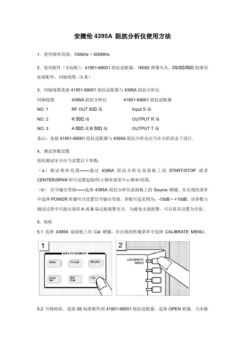
5.校机5.1 选择4395A前面板上的Cal硬键,在出现的软键菜单中选择CALIBRATE MENU。
5.2 开路校机。
连接0S标准配件到41951-69001阻抗适配器,选择OPEN软键。
当本操作实施后,OPEN字样下方会出现下划线,此时可以取下0S标准配件。
5.2 短路校机。
连接0Ω标准配件到41951-69001阻抗适配器,选择SHORT软键。
当本操作实施后,SHORT字样下方会出现下划线,此时可以取下0Ω标准配件。
5.3 50Ω负载校机。
连接50Ω标准配件到41951-69001阻抗适配器,选择LOAD软键。
当本操作实施后,SHORT字样下方会出现下划线。
5.4 选择DONE CAL软键实施校机。
FW354使用手册
抗电快速脉冲群干扰 抗浪涌冲击干扰 抗射频电磁波干扰 抗静电放电干扰
工作温度 工作湿度 存储温度 存储湿度 工作大气压
0.5s (输入自 10%至 90%阶跃变化,进 入稳态 1%带时间)
30 ppm/℃ 指示通信中断,数据保持
指示通道自检错误 ≥120dB ≥60dB
EMC 指标 信号线与地 1kV
备用
COM(绿) 通信指示 无通信
常亮 闪
自检故障 CPU 复位
-正常
工作 试切换
组态不匹 正常
POWER(绿) 5V 电源指示
故障 正常
--
3.2 跳线
状态
跳线
正常使用
程序更新(开发商保 留) 连接传感器 标定调试(开发商保 留)
JP1 跳 1-2 跳 2-3 跳 1-2
--
表 3-2 FW354 卡件跳线
3
FW354 使用手册
工程量的下限值与上限值。
6 故障分析及维护方法
表格 6-1 故障分析及维护方法
序号 1 2
故障特征
FAIL 灯闪、亮 RUN 灯暗 COM 灯暗
FAIL 灯常亮 RUN 灯亮 COM 灯闪
故障原因
CPU 没有正常工作;5V 供电电压偏低
DC/DC 电源不正常,导致 AD 无法正常 工作;CPU 写/读 AD 寄存器校验出错
JP2 跳 1-2 跳 2-3 跳 1-2
--
JP3 跳 1-2 跳 2-3 跳 1-2
--
JP4 跳 1-2 跳 2-3 跳 1-2
--
JP5 第一路 ---
跳 1-2 跳 2-3
JP6 第二路 ---
跳 1-2 跳 2-3
安捷伦34950A使用说明文档
Agilent 34950A64-Bit Digital I/O and Counter Module User’s GuideAgilent Technologies, Inc.Printed in MalaysiaEdition 1June 2008 E0608*34980-90050* 34980-90050Notices© Agilent Technologies, Inc. 2008No part of this manual may be reproduced in any form or by any means (including electronic storage and retrieval or transla-tion into a foreign language) without prior agreement and written consent from Agilent Technologies, Inc. as governedby United States and international copy-right laws.Manual Part Number34980-90050EditionFirst Edition, June 2008Printed in MalaysiaAgilent Technologies, Inc.3501 Stevens Creek BlvdSanta Clara, CA 95052 USAMicrosoft® and Windows® are U.S. regis-tered trademarks of Microsoft Corporation. Software RevisionThis guide is valid for the firmware that was installed in the instrument at the time of manufacture. However, upgrading the firmware may add or change product features. For the latest firmware and documentation, go to the product page at: /find/34980A WarrantyThe material contained in this docu-ment is provided “as is,” and is sub-ject to being changed, without notice,in future editions. Further, to the max-imum extent permitted by applicablelaw, Agilent disclaims all warranties,either express or implied, with regardto this manual and any informationcontained herein, including but notlimited to the implied warranties ofmerchantability and fitness for a par-ticular purpose. Agilent shall not beliable for errors or for incidental orconsequential damages in connectionwith the furnishing, use, or perfor-mance of this document or of anyinformation contained herein. ShouldAgilent and the user have a separatewritten agreement with warrantyterms covering the material in thisdocument that conflict with theseterms, the warranty terms in the sep-arate agreement shall control.Technology LicensesThe hardware and/or software described inthis document are furnished under alicense and may be used or copied only inaccordance with the terms of such license.Restricted Rights LegendU.S. Government Restricted Rights.Software and technical data rights grantedto the federal government include onlythose rights customarily provided to enduser customers. Agilent provides thiscustomary commercial license in Softwareand technical data pursuant to FAR 12.211(Technical Data) and 12.212 (ComputerSoftware) and, for the Department ofDefense, DFARS 252.227-7015 (TechnicalData - Commercial Items) and DFARS227.7202-3 (Rights in Commercial Com-puter Software or Computer SoftwareDocumentation).Safety NoticesA CAUTION notice denotes a haz-ard. It calls attention to an operat-ing procedure, practice, or the likethat, if not correctly performed oradhered to, could result in damageto the product or loss of importantdata. Do not proceed beyond aCAUTION notice until the indicatedconditions are fully understood andmet.A WARNING notice denotes ahazard. It calls attention to anoperating procedure, practice, orthe like that, if not correctly per-formed or adhered to, could resultin personal injury or death. Do notproceed beyond a WARNINGnotice until the indicated condi-tions are fully understood and met.ii A gilent 34950A 64-Bit Digital I/O and Counter Module User’s GuideAdditional Safety NoticesThe following general safety precautions must be observed during all phases of oper-ation of this instrument. Failure to comply with these precautions or with specific warnings or instructions elsewhere in this manual violates safety standards of design, manufacture, and intended use of the instrument. Agilent Technologies assumes no liability of the customer’s failure to com-ply with the requirements.GeneralDo not use this products in any manner not specified by the manufacturer. The protec-tive features of this product may be impaired if it is used in a manner not speci-fied in the operation instructions. Before Applying PowerVerify that all safety precautions are taken. Make all connections to the unit before applying power.Ground the InstrumentThis product is provided with protective earth terminals. To minimize shock hazard, the instrument must be connected to the ac power mains through a grounded power cable, with the ground wire firmly con-nected to an electrical ground (safety ground) at the power outlet. Any interrup-tion of the protective (grounding) conduc-tor or disconnection of the protective earth terminal will cause a potential shock haz-ard that could result in personal injury. Do Not Operate in an Explosive AtmosphereDo not operate the instrument in the pres-ence of flammable gases or fumes.Do Not Remove the Instrument CoverOnly qualified, service-trained personal who are aware of the hazards involved should remove instrument covers. Always disconnect the power cable and any exter-nal circuits before removing the instrument cover. Do Not Modify the InstrumentDo not install substitute parts or performany unauthorized modification to the prod-uct. Return the product to an Agilent Salesand Service Office for service and repair toensure that safety features are maintained.In Case of DamageInstruments that appear damaged or defec-tive should be made inoperative andsecured against unintended operation untilthey can be repaired by qualified servicepersonnel.Safety SymbolsWaste Electrical and ElectronicEquipment (WEEE) Directive2002/96/ECThis product complies with the WEEEDirective (2002/96/EC) marking require-ment. The affixed product label (see above)indicates that you must not discard thiselectrical/electronic product in domestichousehold waste.Product Category: With reference to theequipment types in the WEEE directiveAnnex 1, this product is classified as a“Monitoring and Control instrumentation”product.To return unwanted products, contactyour local Agilent office, or go to/environment/productfor more information.Technical SupportIf you have questions about your shipment,or if you need information about warranty,service, or technical support, contactAgilent Technologies:In the United States: (800) 829-4444In Europe: 31 20 547 2111In Japan: 0120-421-345Or go to /find/assistfor information on contacting Agilent inyour country of specific location. You canalso contact your Agilent TechnologiesRepresentative.Alternating currentFrame or chassisterminalStandby supply. Unit isnot completelydisconnected from acmains when switch is offCaution, risk of electricshockCaution, refer toaccompanying descriptionAgilent 34950A 64-Bit Digital I/O and Counter Module User’s Guide iiiThe Declaration of Conformity(DoC) for the 34980A mainframe instrument can be found on page iii in the 34980A Mainframe User’s Guide. That DoC applies to the 34980A mainframe and all available plug-in modules.Contents34950A 64-Bit Digital I/O Module with Memory and Counter . . . . . . . . . . .. . . . . . . . . . . .1 Bank and Channel Assignments . . . . . . . . . . . . . . . . . . . . . . . . . . . . . . . . .. . . . . . . . . . . .1Electrical Characteristics for Digital I/O Lines . . . . . . . . . . . . . . . . . . . . .. . . . . . . . . . . .2Operating Considerations. . . . . . . . . . . . . . . . . . . . . . . . . . . . . . . . . . . . . . .. . . . . . . . . . . .2Basic Digital I/O Operations . . . . . . . . . . . . . . . . . . . . . . . . . . . . . . . . . . . . . . .. . . . . . . . . . . .3 Channel Numbering and Width . . . . . . . . . . . . . . . . . . . . . . . . . . . . . . . . . .. . . . . . . . . . . .3Reading Digital Data . . . . . . . . . . . . . . . . . . . . . . . . . . . . . . . . . . . . . . . . . . .. . . . . . . . . . . .4Writing Digital Data . . . . . . . . . . . . . . . . . . . . . . . . . . . . . . . . . . . . . . . . . . .. . . . . . . . . . . .5Channel Width and Polarity, Threshold, Level, and Drive . . . . . . . . . . . .. . . . . . . . . . . .6 Handshaking. . . . . . . . . . . . . . . . . . . . . . . . . . . . . . . . . . . . . . . . . . . . . . . . . . . . .. . . . . . . . . . . .7 Setting the Handshake Line Parameters . . . . . . . . . . . . . . . . . . . . . . . . . .. . . . . . . . . . . .8Synchronous Handshake Mode. . . . . . . . . . . . . . . . . . . . . . . . . . . . . . . . . .. . . . . . . . . . . .9Buffered I/O Operations. . . . . . . . . . . . . . . . . . . . . . . . . . . . . . . . . . . . . . . . . . .. . . . . . . . . . .14 Buffered (Memory) Output. . . . . . . . . . . . . . . . . . . . . . . . . . . . . . . . . . . . . .. . . . . . . . . . .14Deleting Trace . . . . . . . . . . . . . . . . . . . . . . . . . . . . . . . . . . . . . . . . . . . . . . . .. . . . . . . . . . .16Buffered (Memory) Input . . . . . . . . . . . . . . . . . . . . . . . . . . . . . . . . . . . . . . .. . . . . . . . . . .16 Interrupt Lines . . . . . . . . . . . . . . . . . . . . . . . . . . . . . . . . . . . . . . . . . . . . . . . . . . .. . . . . . . . . . .18 Memory Output Operations . . . . . . . . . . . . . . . . . . . . . . . . . . . . . . . . . . . . .. . . . . . . . . . .18Memory Input Operations. . . . . . . . . . . . . . . . . . . . . . . . . . . . . . . . . . . . . . .. . . . . . . . . . .19 Byte Ordering . . . . . . . . . . . . . . . . . . . . . . . . . . . . . . . . . . . . . . . . . . . . . . . . . . . .. . . . . . . . . . .20Pattern Matching . . . . . . . . . . . . . . . . . . . . . . . . . . . . . . . . . . . . . . . . . . . . . . . .. . . . . . . . . . .21Counter . . . . . . . . . . . . . . . . . . . . . . . . . . . . . . . . . . . . . . . . . . . . . . . . . . . . . . . . .. . . . . . . . . . .22 Totalizer Mode . . . . . . . . . . . . . . . . . . . . . . . . . . . . . . . . . . . . . . . . . . . . . . . .. . . . . . . . . . .22Initiated Measurement Mode . . . . . . . . . . . . . . . . . . . . . . . . . . . . . . . . . . .. . . . . . . . . . .23Threshold Voltages . . . . . . . . . . . . . . . . . . . . . . . . . . . . . . . . . . . . . . . . . . . . . . . . . . . . . . .23 Clock. . . . . . . . . . . . . . . . . . . . . . . . . . . . . . . . . . . . . . . . . . . . . . . . . . . . . . . . . . . .. . . . . . . . . . .2434950A D-Sub Connectors . . . . . . . . . . . . . . . . . . . . . . . . . . . . . . . . . . . . . . . . .. . . . . . . . . . .2534950T Terminal Block . . . . . . . . . . . . . . . . . . . . . . . . . . . . . . . . . . . . . . . . . . . .. . . . . . . . . . .2734950A 64-Bit Digital I/O Module with Memory and Counter34950A 64-Bit Digital I/O Module with Memory and CounterThe 34950A has 64-bits of general-purpose digital I/O grouped in 8-bitchannels with programmable polarity, input thresholds, and output levels.The module is segmented into two banks of four 8-bit channels. Each bankhas 64 Kb of volatile memory for pattern capture and pattern generationwith hardware interrupt capability. Up to three pins of handshaking areavailable for each bank of 32 bits.The module also has two 10 MHz frequency counter/totalizer measurementinput channels and a programmable clock output for frequencysynchronization or general clocking needs.Bank and Channel AssignmentsThe digital channels are numbered by bank; 101 through 104 and 201through 204 for banks 1 and 2 respectively. The counter/totalizer channelsare assigned channel numbers 301 and 302. The programmable clock is not34950A 64-Bit Digital I/O Module with Memory and CounterElectrical Characteristics for Digital I/O LinesThe following simplified schematic shows the interface circuitry and specifications for each of the 64 digital I/O lines:Operating ConsiderationsSee the Introduction to the Plug In Modules chapter of the 34980A Mainframe User’s Guide for detailed environmental operating conditions for the 34980A mainframe and its installed modules. That guidance sets maximum per channel current and power ratings at rated voltage for pollution degree 1 (dry) and pollution degree 2 (possible condensation) conditions, for the Digital I/O module.Active Drive:V in 0V – 5VV out (L) 0.24V < V out < 0.55V 4mA < I out < 24mA V out (H)1.6V < V out < 5V -4mA < I out < -24mAOpen Collector:V out0V – 5V-4 mA < I out < -24mA V cc (< 2V)V cc (> 2V)215 Ω < R pullup < 1 k Ω215 Ω < R pullup < 10 k ΩBasic Digital I/O Operations Basic Digital I/O OperationsChannel Numbering and WidthThe digital channels are numbered by bank; 101 through 104 and 201through 204 for banks 1 and 2 respectively.Using SCPI commands you can group digital I/O channels together toallow 16- or 32-bit operations. The first and third channels on a bank canbe control channels. Width and direction of the memory operations arecontrolled by the width and direction of the first channel on the bank(i.e., 101 or 201). In the SCPI language for the 34950A, BYTE refers to8-bit operations, WORD refers to 16-bit operations, and LWORd refers to32-bit operations.This table illustrates how the channels are numbered for each operatingconfiguration.Bank 1Bank 2ChannelBYTE (default)1011021031042012022032048-bits8-bits8-bits8-bits8-bits8-bits8-bits8-bitsWORD10110320120316-bits16-bits16-bits16-bitsLWORd10120132-bits32-bitsBasic Digital I/O OperationsReading Digital DataThe simplest way to read a digital channel is using the MEASure:DIGital?query. This query sets the channel to be an input channel and sets allother channel parameters to the default settings.For example, sending the following SCPI command to a Digital I/O moduleinstalled in slot 1 of the mainframe will read the value of the 8-bitchannel 102. An unsigned integer value is returned that represents thestate of the 8 bits on channel 102.MEAS:DIG? BYTE, (@1102)By adding parameters to the command, you can set the channel width,polarity, and threshold for read. For example, sending the following SCPIcommand you can read the 32-bit channel 201.MEAS:DIG? LWOR, (@1201)To read digital data with more control over the channel parameters,use the SCPI CONFigure and SENSe commands. The CONFigure commandsset up the digital I/O channel parameters. For example, sending thefollowing SCPI command to a Digital I/O module installed in slot 1 of themainframe, sets a 16-bit input channel (103) to use a 2.5 V inputthreshold, and normal polarity.CONF:DIG WORD, 2.5, NORM, (@1103)Once configured, the data is read using the following command.SENS:DIG:DATA:WORD? (@1103)You may also read an individual bit using the SENSe commands.This allows you to check the state of an individual bit in a channelwithout having to create an input mask. For example, the followingcommand returns the state of bit 3 in the channel 101 byte.SENS:DIG:DATA:BIT? 3, (@1101)The acceptable range for the bit parameter is based on the channel widthas shown below:•BYTE (8-bit): <bit> can range from ‘0’ to ‘7’•WORD (16-bit): <bit> can range from ‘0’ to ‘15’•LWORd (32-bit): <bit> can range from ‘0’ to ‘31’The SENSe command differs from the MEASure command in that it will notchange the direction (input or output) of the channel. If the channel isconfigured as an output, the SENSe command will return the value beingdriven.Basic Digital I/O OperationsWriting Digital DataTo write digital data, set the channel output parameters using the SOURcecommands. For example, sending the following SCPI commands to a DigitalI/O module in slot 1 sets a 32-bit channel to use normal polarity,with active drive and a ‘set’ output voltage of 4 volts.CONF:DIG:WIDT LWOR,(@1201)CONF:DIG:POL NORM,(@1201)SOUR:DIG:DRIV ACT,(@1201)SOUR:DIG:LEV 4,(@1201)The width and polarity parameters apply to both input and output operations.You can set a channel to output in either active drive or open collectorconfigurations. When set to ACTive, the module drives the digital lines for bothhigh and low. The voltage level that represents a logic ‘1’ can be set using theSOURce:DIGital:LEVel command. Output voltages can range from 0.80 V(default) to 5 V.When the channel is set to OCOLlector, lines are driven low, but set to highimpedance (Hi-Z) when asserted. In the open collector mode, multiple linescan be connected together by providing external pull-ups.When using external pull-ups in the open collector mode, the outputs willnot exceed 5 V.Once a channel has been configured, write digital data to the channel using theSOURce:DIGital:DATA command.SOUR:DIG:DATA:LWOR 26503,(@1201)You may also use a hexadecimal format to represent values in the commands.For example, to send the decimal value of 26503 in hex use the command form:SOUR:DIG:DATA:LWOR #h6787,(@1201)Writing to a channel automatically configures the channel as an output.Note that the data should match the channel width configured usingCONFigure:DIGital:DATA:WIDTh command. The data written is maskedby the configured width so that any extra bytes will be discarded.For example: sending the value 65531 to a byte wide channel will resultin the channel discarding the upper byte and outputting 251.Basic Digital I/O OperationsChannel Width and Polarity, Threshold, Level, and DriveWhen the width of a channel is set to WORD or LWORd, the channeldirection (input or output) of the channels spanned by the width iscontrolled by the channel in operation. That is, all grouped channels areautomatically set to the same input or output operation.Channel settings of polarity, threshold, level, and drive mode areunchanged when channels are combined. For example, consider thefollowing command sequence.CONF:DIG:POL NORM,(@1101)CONF:DIG:POL INV,(@1102)CONF:DIG:WIDT WORD,(@1101)This command sequence set the first 8 bits (channel 101) to normalpolarity for input and output operations, set the next 8 bits (channel 102)to inverted polarity, and then combines the bits into a 16-bit channel.When this WORD channel is used, the first eight bits will input or outputusing normal polarity but the next 8 bits will read or written usinginverted polarity.Threshold, level, and drive settings all behave in the same manner as thepolarity setting described above.HandshakingHandshakingHandshaking provides a means to synchronize the input or output ofdigital data. By default, no handshaking is used; data is input or output as the command is executed. The handshake is configured per bank.The 34950A provides a synchronous handshake mode (strobe handshake). You can use this mode with basic input and output operations. You must use this handshake mode to use buffered I/O (see “Buffered I/OOperations” on page 14).The handshake is performed using three lines on each bank. The lines are labeled H0, H1, and H2. The function of each line is set by the input or output mode in use. Since there are only three handshake lines per bank, the SCPI handshake commands are only valid for the first channel in a bank. Once handshaking is enabled, it applies to the width of the first channel in the bank.The three handshaking lines on each bank also differ slightly if you are using buffered (memory) I/O (see page 14) or unbuffered I/O operations. You can also perform unbuffered operations without any handshake. The function of each line for each mode of operation is defined in the table below.The following handshake command sets the synchronous handshaking mode for the channels in bank 1.CONF:DIG:HAND SYNC, (@1101)This form of the handshaking command also allows you to optionally set the input threshold, output drive level, and polarity of all the handshake lines. For example, the following command sets bank 2 to use synchronous handshaking, with an input threshold of 2.5 V, an output drive level of2.5 V, and normal polarity. Other parameters such as the handshake timing are set to default values (refer to the Programmer’s Reference Help file for details ).CONF:DIG:HAND SYNC, 2.5, 2.5, NORM, (@1201)H0H1H2Unbuffered Synchronous Input I/O Direction (output)Strobe (output)Not Used (Hi-Z)Unbuffered SynchronousOutputI/O Direction (output)Strobe (output)Not Used (Hi-Z)Buffered Synchronous Input Start/Stop (output)Not Used (Hi-Z)Input Strobe (input)Buffered Synchronous Output (internal clock)Start/Stop (output)Strobe (output)Not Used (Hi-Z)Buffered Synchronous Output (external clock)Start/Stop (output)Not Used (Hi-Z)Output Strobe (input)HandshakingYou can set parameters by using a sequence of commands instead of theCONFigure macro command. For example, the following command sequencesets the handshaking mode to synchronous, the output drive to opencollector, and the handshake rate to 1 MHz.CONF:DIG:HAND:MODE SYNC, (@1101)CONF:DIG:HAND:DRIV OCOL, (@1101)CONF:DIG:HAND:RATE 1000000, (@1101)Setting the Handshake Line ParametersYou can set the handshake lines’ input threshold, output drive mode, andoutput drive voltage. These settings affect all the handshake lines in thebank. Handshake line polarity can be set for each individual handshakeline.For example, you can invert the polarity of the handshake line H1 onbank 2 with the following command.CONF:DIG:HAND:POL INV, H1, (@1201)You can set the output drive mode, output voltage, and input threshold forall handshake lines in each bank. For example, the following commands setthe drive mode to active, the drive voltage to 4.5 V, and the inputthreshold to 1.0 V on bank 2.CONF:DIG:HAND:DRIV ACT, (@1201)SOUR:DIG:HAND:LEV 4.5, (@1201)SENS:DIG:HAND:THR 1, (@1202)The settings for drive mode, output drive level, and input threshold alsoapply to the bank’s interrupt line.When using external pull-ups in the open collector mode, the outputs willnot exceed 5 V.HandshakingSynchronous Handshake ModeIn the synchronous handshake mode, a strobe or clock signal is used totransfer data to or from an external device. The strobe line (H1) is anoutput and is pulsed once for each transfer.Synchronous Unbuffered InputsFor synchronous handshake unbuffered inputs the H0 line indicates thedirection of the transfer. This line is set high to indicate an inputoperation. The H0 line will remain in the high state until the 34950Adirection is changed. The H1 line is the strobe output line. The H2 line isnot used and is set to high impedance.The timing of the input operation is controlled by the T CYCLE parameterset using the CONFigure:DIGital:HANDshake:RATE command. This settingaffects strobe width, memory clock rate, as well as the setup and holdtimes. Alternatively, the reciprocal form of the commandCONFigure:DIGital:HANDshake:CTIMe can be used to specify the speed interms of time instead of a rate. T CYCLE begins when the 34950A executesone of the input commands.The timing should be set such that the device sending the data ensuresthe data lines are valid prior to T SETUP time. The trailing edge of thestrobe line indicates the 34950A will latch the data within the T HOLD time.T SETUP is 90 ns and T HOLD is 0 ns. Since T HOLD = 0 µs, the sending devicecan use the trailing edge of the strobe to initiate a change in the datalines.A synchronous unbuffered input is shown in the diagram belowFor example, the following SCPI commands set a 34950A in slot 5 to havea 16-bit input using synchronous handshake. Two data inputs are thenperformed and the strobe line is pulsed for each query. The I/O directionline is set high following the first SENSe:DIGital:DATA:WORD? query andremains high until the digital channel is reset or reconfigured.CONF:DIG:WIDT WORD, (@5101)CONF:DIG:DIR INP, (@5101)CONF:DIG:HAND SYNC, (@5101)SENS:DIG:DATA:WORD? (@5101)SENS:DIG:DATA:WORD? (@5101)HandshakingSynchronous Unbuffered OutputsFor synchronous handshake unbuffered outputs, the H0 line indicates thedirection of the transfer. This line is set low to indicate an outputoperation. The H0 line will remain in the low state until the 34950Adirection is changed. The H1 line is the strobe output line.When the 34950A executes an output command, it sets the data lines andwaits for T CYCLE/2 before asserting the strobe line. The leading edge of thestrobe indicates the data is valid. The strobe line is asserted for T CYCLE /2and then de-asserted. The H2 line is not used and is set to highimpedance.The timing of the output operation is controlled by the T CYCLE parameterset using the CONFigure:DIGital:HANDshake:RATE command. This settingaffects strobe width, memory clock rate, as well as the setup and holdtimes. Alternatively, the reciprocal form of the commandCONFigure:DIGital:HANDshake:CTIMe can be used to specify the speed interms of time instead of a rate. The timing should be set such that thedevice receiving the data can read the data lines during the T CYCLE/2 time.A synchronous unbuffered output is shown in the diagram below (defaultFor example, the following SCPI commands set a 34950A in slot 5 to havea 16-bit output using synchronous handshake. Two data outputs are thenperformed and the strobe line is pulsed for each. The I/O direction line isset low following the first SOURce:DIGital:DATA:WORD command andremains low until the digital channel is reset of reconfigured.CONF:DIG:WIDT WORD, (@5101)CONF:DIG:DIR OUTP, (@5101)CONF:DIG:HAND SYNC, (@5101)SOUR:DIG:DATA:WORD #hFFFF, (@5101)SOUR:DIG:DATA:WORD #h4DB5, (@5101)HandshakingSynchronous Buffered InputsYou can use synchronous mode handshake with buffered (memory) input operations. (Buffered operations are described in more detail beginning on page 14.) For buffered input operations, the H0 line acts as a start/stop line. This line will be set high when the memory input command is executed and will return low when the memory input operation has completed. The H1 line is not used and is set to high impedance.An external strobe input on the H2 line controls the pace of memory transfers. The sending device must ensure the data is valid before theT SETUP and stays valid until after T HOLD. T SETUP is 46 ns and T HOLD is10 ns.A synchronous buffered input using an external clock is shown in the diagram below (default handshake line polarity).For example, the following SCPI commands set a 34950A in slot 5 to have an 8-bit input using synchronous handshake with an external strobe input. The number of bytes to read into memory is set to infinite (continuous reading into memory until the memory is stopped). The memory is enabled and then triggered. The start/stop line is set high following the first byte handshake and remains high until the last byte is captured. CONF:DIG:WIDT BYTE, (@5101)CONF:DIG:DIR INP, (@5101)CONF:DIG:HAND SYNC, (@5101)SENS:DIG:MEM:SAMP:COUN 0, (@5101)SENS:DIG:MEM:ENAB ON, (@5101)SENS:DIG:MEM:STAR (@5101)HandshakingSynchronous Buffered OutputsYou can use synchronous mode handshake with buffered (memory) outputoperations. (Buffered operations are described in more detail beginning onpage 14.) For buffered output operations, the H0 line acts as a start/stopline. This line will be set high when the memory output command isexecuted by the 34950A and will return low when the memory outputoperation has completed.Synchronous memory output operations can be paced using either theinternal strobe or an external strobe.When using the internal strobe, the H1 line is the strobe output line.The timing of the output operation when using the default INTernal clockis controlled by the CONFigure:DIGital:HANDshake:RATE command.This setting affects strobe width, memory clock rate, as well as the setupand hold times. Alternatively, the reciprocal form of the commandCONFigure:DIGital:HANDshake:CTIMe can be used to specify the speed interms of time instead of a rate. The timing should be set such that thedevice receiving the data can latch the data lines during the T CYCLE time.The receiving device should detect the leading edge of the strobe line, waitfor the 34950A to set the data (T PD) and then latch the data. Latching thedata on the trailing edge of the strobe is recommended, however, you canthe data following T PD. T PD ranges from -23 to 23 ns.A synchronous buffered output using the internal clock is shown in thediagram below (default handshake line polarity).。
新亚科技 NA9353E 使用说明说明书
NA9353E 使用说明(V1.2)安装注意事项1、面板与控制器通信线如需延长请使用四芯屏蔽双绞线,长度不要超过300m。
2、双库温探头请绑在一起,放置在冷风机回风处,距离冷风机背面或者下方20cm处,不要靠近库板及货物密集区域。
3、化霜温度探头建议固定在冷风机回气管上,距离冷风机不超过10cm,并用保温管包住。
4、请使用本公司配套生产的互感线圈。
5、“压控开关”、“库门开关”均为无源通断信号,严禁带电接入。
6、请使用本公司配置的温度探头,如需对温度探头进行延长接线(延长线不要超过10m),请使用双芯屏蔽线焊接,连接处做好绝缘处理。
7、以上所有涉及的布线均为弱电信号线,不能与强电信号线、供电主线混在一起布线,否则可能干扰控制器正常运行。
主要功能及技术指标主要功能:一、控制功能:1、控制压缩机:根据开、停机温度控制压缩机启停,两路温控探头同时故障时可以按设定的开停时间定期运行。
2、控制化霜:可设置周期化霜、北京时间化霜和强制化霜;化霜结束条件为温度和时间双重控制,可设置化霜滴水时间。
3、控制冷风机:可设置跟随压缩机控制、根据化霜温度控制等五种运行模式。
二、告警保护功能:1、高、低温告警:可设定高、低温告警温度,温度过高或过低时产生告警。
2、压缩机保护:压缩机过载保护,欠载保护,电流不平衡保护。
3、冷风机保护:冷风机过载保护,电流不平衡保护。
4、供电保护:供电缺相、错相保护。
5、外部告警保护:可接压控开关,压缩机模块开关等开关量保护装置。
6、库门开启提醒:需外接库门开关;通过库门开关可实现开门时系统待机功能。
三、远程功能:1、远程查看数据:手机APP端及电脑网页端双平台查看实时数据、机组状态、温度曲线、历史数据等。
2、远程控制设备:手机APP端及电脑网页端双平台设置参数、开关机、强制化霜、权限管理等操作。
3、峰谷电运行模式:当峰谷电工作模式开关打开时,系统在设定的时段内以峰谷电工作模式运行,利用该功能可实现让设备只在设定的时段内工作。
全面型呼吸防护器
Jupiter特点
扁轮廓设计,适合狭小空间作业 大流量,最低设计流量150升/分 可选本质安全配置 可选防尘/尘毒组合 滤料盖设计防液体喷溅,阻隔粗粉尘,延长主滤棉使用寿命 自上向下气流避免面镜起雾 提供流量检验(白球流量计) 多种头罩/头盔选择,适应性强 坚固耐用,零部件少,外形流畅,易于清洁,低保养需求 预过滤棉延长主滤棉寿命 提供低流量及低电量声光报警
• 充满电的Jupiter镍氢电池储存在室温条件下,每天大约损失2%的电量,一个星期大约损失 10%电量,一个月大约损失20%电量。存放温度升高,自我放电率也将增加;
• 不常使用的Jupiter电池如果不是一直连接在充电器上充电,应该在下次使用前,充分充电 ,然后每个月充分充电一次以维持电量;在储存周期中(少于1年),允许电池自己放电将不 会破坏电池,但如果电池一直长时间存放不用(长于1年),将失去可以维持满电量的能力。
+
Jupiter
DM
HT- 840
防液体喷溅时不建议用 HT-101/103,需要考虑 颈部有覆盖的头罩。
HT-100系列头罩
HT-101
轻质随弃式头罩; 白色聚丙烯材质; 宽视野面镜; 指定防护因数:25
HT-103
轻质头罩; 耐用灰色尼龙有纺基层材质,低保养; 宽视野面镜; 指定防护因数:25
Jupiter & DM适用的头罩和头盔
100 Series
400 Series 700 Series 800 Series(视窗防熔融金属)
HT-101 HT-103
HT-120
HT- 401 (A)
HT-770011
HT-770022
- 1、下载文档前请自行甄别文档内容的完整性,平台不提供额外的编辑、内容补充、找答案等附加服务。
- 2、"仅部分预览"的文档,不可在线预览部分如存在完整性等问题,可反馈申请退款(可完整预览的文档不适用该条件!)。
- 3、如文档侵犯您的权益,请联系客服反馈,我们会尽快为您处理(人工客服工作时间:9:00-18:30)。
NA9354使用说明(V1.1)主要功能及技术指标主要功能:一、具备温度控制功能:1、控制压缩机开停:温度显示、温度控制、压缩机开机延时保护、温控探头故障告警、两路温控探头同时故障时可以按设定的开停比定期运行。
2、控制化霜:温控化霜、周期化霜、北京时间化霜。
化霜结束条件为温度和时间双重控制、化霜滴水、化霜探头故障告警。
备注:也可使用“手动进入或退出化霜”功能。
3、控制冷风机:由化霜温度控制、跟随压缩机控制等五种运行模式可设置。
二、具备以下保护功能:1、高低温告警:可设定高低温告警温度,温度过高或过低时产生告警。
2、电机过载保护:可显示压缩机运行电流,当电流超过设定的过载电流及三相电流严重不平衡时,保护电路动作,断开负载,保护压缩机。
3、冷风机保护:当电流超过设定的过载电流及三相电流严重不平衡时,保护电路动作,断开负载,保护冷风机。
4、电压缺相错相保护:三相输入电压缺相、错相时,保护电路动作,断开负载。
5、未关冷库门提醒:记录库门开启的次数和时间。
(需要安装门开关,并将信号线接入控制器)6、外部告警控制:可根据外部告警信号的形式,选择四种外部告警信号输入模式。
7、告警输出:当出现告警时,控制器提供一路开关量输出信号,用于外接报警器。
三、基于远程管理条件下具备的功能:1、用电量统计:查看冷库每天、每月或一段时间内的用电量。
2、月报表推送:每月初向业主手机发送冷库上月的三项指标:安全指标、能耗指标、日常管理指标。
便于业主随时了解冷库的现状。
3、峰谷电运行模式:当峰谷电工作模式开关打开时,系统在设定的时段内以峰谷电工作模式运行。
备注:使用该功能时,请注意储品的存储温度,避免温度过低对冻品造成伤害。
4、冷库断电提醒:当冷库关闭电源或异常断电的情况,控制器会自动发出断电提醒。
备注:本通讯模块为嵌入式GSM/GPRS通讯模块,无需插卡。
主要技术指标:温度显示范围: -45~120℃温度设定范围: -40~115℃电流显示范围: 0~100A电流设定范围: 0~80A控制器电源: AC380V,三相四线制使用环境:温度-20℃~60℃;湿度≤85%,无凝露,无腐蚀输出触点容量: 5A/250VAC温度传感器: NTC R25=5kΩ,B(25/50)=3470K执行标准: Q/320585 XYK 01 Q/320585 XYK 03 Q/320585 XYK 04操作指南面板显示框图示☝面板上的指示灯含义是什么?2数码管显示含义数码管在正常时显示冷库温度,告警时交替显示冷库温度和告警代码(Axx),显示代码如下表:3注意:库温探头1和库温探头2都故障时,告警停机,手动恢复。
数码管长显示“- - - -”表示面板与主控板通信异常。
*注:排除故障后按面板任意键进行告警复位并自动开机1、系统解锁系统上电后进入调试阶段,调试时间固定为2小时,之后系统将会自动停机并锁定,控制面板上交替显示“LOC”与当前冷库温度。
用户需用手机扫描电控箱体二维码,下载远程监控客户端进行注册,然后根据电控箱体提示获取“开机码”,或者直接联系电控箱厂商获取开机码。
按住“SET”键不放保持5秒控制面板显示“0000”,按“SET”键光标可在四位数字中切换,按“ ”或“ ”键上下调节数字大小,按住“SET”键不放保持2秒进行开机码输入确认,开机码保持3秒后控制面板长显示温度,如不再显示“LOC”,表示系统已激活,按照控制器参数内容说明及修改操作说明进入“开机码(F90)”可查看输入的开机码。
用户也可以直接设置参数“开机码(F90)”激活系统,无需等待调试阶段。
注意:在2小时的调试阶段内,如果系统还未输入正确的开机码,控制面板会每间隔30显示“LOC”,并且蜂鸣器告警(持续5秒)指示系统还未激活。
2、按键锁定和解锁2.1、按键未操作时间超过30秒,锁形图标“”长亮,所有操作按键锁定。
42.2、在按键锁定状态下,按住“SET”键不放保持3秒,锁形状图标“”灭掉,按键解锁,所有按键恢复正常使用。
3、怎样开/关机在按键解锁状态,且无停机告警时按住“ON/OFF”键不放保持5秒系统开机,按住“ON/OFF”键不放保持5秒系统关机。
4、怎样快速设置开/停机温度、化霜周期、化霜持续时间按“SET”键进入快速设置状态,按“ ”或“ ”可在开机温度、停机温度、化霜周期、化霜持续时间4个参数项中来回切换,按“SET”键参数闪烁后按“ ”或“ ”键可上下调节参数值(长按“ ”或“ ”键可快速上下调节参数值),调节到所需参数后按“SET”键确认参数,根据状态指示灯提示可依次设置开机温度、停机温度、化霜周期、化霜持续时间,全部设置完成后自动退出设置状态,设置过程中也可以按“ON/OFF”键直接退出设置状态。
注意:1、在设置状态,如果连续20秒没有按键,则自动退出设置状态,但不保存当前未确认的参数。
2、必须确认参数才能确保将设定参数值保存起来。
如果在确认参数之前断电,则当前调节的参数没有保存。
5、怎样进行强制化霜按住“ ”键不放保持5秒,则进入强制化霜状态。
在化霜时按住“ ”键不放保持5秒,能强制结束化霜。
6、怎样查看库温探头2温度、压缩机运行电流和用电量在显示库温时按下“ ”键,就会切换显示库温探头2温度、压缩机运行电流(在化霜时显示化霜电流)及系统用电量。
松开“ ”键则恢复显示冷库温度。
7、怎样查看冷风机电流、化霜温度在显示库温时按下“ ”键,就会切换显示化霜温度和冷风机电流。
松开“ ”键则恢复显示冷库温度。
注意:如果按住“ ”键不放保持5秒会进入强制化霜。
8、怎样查看及设置时间进入系统参数表(详见控制器参数内容说明及修改操作说明),F96为系统时间参数“时:分”,F97为系统时间参数“月日”,F98为系统时间参数“年”。
9、控制器参数内容说明及修改操作说明9.1 本控制器可以对一些内部参数进行调整,以适应不同的需要。
这些参数是为专业技术人员提供的,普通用户不必了解。
也请非专业人员不要随便改变控制器的内部参数,以免造成控制器工作异常。
9.2 在显示状态下,按住“SET”键不放保持5秒,可进入参数设置状态,如果设置了口令,数码管会显示“0000”,用“ 、 、SET”键输入每一位口令后按住“SET”键不放保持2秒,如果口令正确,会显示参数代码“F00”,表示进入高级参数菜单,用“ 、 ”键选择参数代码,选择一个要设置的代码后按“SET”键对该代码参数值进行设置,按“ ”或“ ”键可上下调节参数值(按住“ ”或“ ”键不放可快速上下调节参数值),调节到所需参数值后按“SET”键确认参数,按“ON/OFF”可退出参数设置状态(连续20秒没有操作按键,则自动退出设置5状态)。
注意:参数改变后要按“SET”键回到“Fxx”状态才会被保存。
参数代码明细表:67*注:“压缩机运行频率”在两个库温探头都故障时起作用,让压缩机工作在保护运转状态,在这个状态下,以30分钟为一个周期,压缩机运转F22 x 3分钟,停止30 – (F22 x 3)分钟,例如: F22设置为3,则当两个温控探头发生故障时压缩机运转9分钟,停21分钟,如此循环。
如果不需要此功能,可将F22设为0。
基本工作原理1、制冷控制温度控制根据“开机温度(F11)”和“停机温度(F12)”两个参数进行。
当温控探头上感知到的温度高于“开机温度(F11)”时启动制冷,直到温度低于“停机温度(F12)”时停止制冷,将冷库温度控制在“开机温度(F11)”和“停机温度(F12)”之间。
82、峰谷电工作模式“峰谷电工作模式开关(F70)”设置1可打开峰谷电工作模式,在“谷电模式开始时间(F73)”和“谷电模式结束时间(F74)”设定的时段内,温度控制根据“谷电模式开机温度(F71)”和“谷电模式停机温度(F72)”两个参数进行。
当温控探头上感知到的温度高于“谷电模式开机温度(F71)”时启动制冷,直到温度低于“谷电模式停机温度(F72)”时停止制冷,将冷库温度控制在“谷电模式开机温度(F71)”和“谷电模式停机温度(F72)”之间。
注意:该工作模式需要远程监控功能支持。
3、压缩机开机延时保护控制器内有一个“压缩机停机计时器”,当压缩机停机时开始计时,下一次启动压缩机前首先检查这个计时器,如果已满三分钟则立即启动压缩机,如果不满三分钟则等满三分钟再启动。
这样可以保证停机后再启动间隔大于三分钟,防止频繁启动损坏压缩机。
另外控制器刚通电的三分钟之内也不会启动压缩机,这样在突然停电再来电的情况下也能保护压缩机。
注意:上述的“三分钟”为“压缩机停机保护时间(F21)”默认参数,用户可调。
4、自动化霜控制4.1 控制器有2种化霜模式(F30):1、F30=0时,控制器根据“化霜周期(F31)”设定的时间定时启动化霜(时间为压缩机累计运行时间)。
2、F30=1时,控制器根据“化霜北京时间(F61、F62、F63)”设定的北京时间段启动化霜。
4.2 化霜启动后控制器会通过化霜温度探头检查化霜效果,如果探头温度达到“化霜结束温度”则认为化霜完毕,结束化霜。
如果化霜时间过长,超过了“化霜持续时间(F33)”,控制器将强制结束化霜。
4.3 控制器有2种化霜方式(F36):1、F36=0时,电化霜方式。
2、F36=1时,热氟化霜方式。
5、化霜滴水可以设定一个“化霜滴水时间(F34)”,例如设为5分钟,则化霜结束后5分钟内不会启动制冷。
注意:任何方式结束化霜,都需要化霜滴水。
6、冷风机控制冷风机共有五种运行模式(“冷风机模式(F41)”):0: 关闭冷风机。
1:在制冷状态,冷风机跟随压缩机状态,压缩机启动后冷风机延时启动,延时时间由“冷风机提前/延时启动时间(F42)”设定;压缩机停止后冷风机延时停止,延时时间由“冷风机延时停止时间(F43)”设定。
2:冷风机受化霜温度控制,低温开高温停,由“冷风机启动温度(F44)”和“冷风机启动温度回差(F45)”设定,当化霜温度低于F44时开冷风机,到温度高于F44+F45时关冷风机。
3:压缩机开时开冷风机,压缩时停时风机定时启停,启停时间由“冷风机开时间(F46)”和“冷风机停时间(F47)”设定,即开F46分钟,停F47分钟。
4:冷风机常转,但在发生停机告警时停止。
7、压缩机及化霜电流检测控制器通过专用的互感线圈检测制冷及化霜总回路的电流值,当制冷时显示压缩机电流,当化霜时显示化霜电流。
98、压缩机过载保护8.1 当负载平均电流超过“压缩机过载电流(F51)”,并且达到设定的“过载告警延时(F53),则触发过载告警。
为了避开电机的启动电流,过载告警延时要大于电机启动时间。
8.2 为了防止误动作,过载告警触发后,可自动恢复2次,若连续3次触发过载告警,则保护电路动作,断开负载,系统停机,产生告警。