单片机外文文献翻译
单片机-外文翻译-外文文献-英文文献-单片机简介-中英对照电子教案
Single chip brief introductionThe monolithic integrated circuit said that the monolithic micro controller, it is not completes some logical function the chip, but integrates a computer system to a chip on. Summary speaking: A chip has become a computer. Its volume is small, the quality is light, and the price cheap, for the study, the application and the development has provided the convenient condition. At the same time, the study use monolithic integrated circuit is understandsthe computer principle and the structure best choice.The monolithic integrated circuit interior also uses with the computer function similar module, for instance CPU, memory, parallel main line, but also has with the hard disk behave identically the memory component7 what is different is its these part performance is opposite our home-use computer weak many, but the price is also low, generally does not surpass 10 Yuan then Made some control electric appliance one kind with it is not the 'very complex work foot, We use now the completely automatic drum washer, the platoon petti-coat pipe: VCD and so on Inside the electrical appliances may see its form! It is mainly takes the control section the core part.It is one kind of online -like real-time control computer, online -like is the scene control, needs to have the strong antijamming ability, the low cost, this is also and the off-line type computer (forinstance home use PC,) main differenceThe monolithic integrated circuit is depending on the procedure, and may revise. Realizes the different function through the different procedure, particularly special unique some functions, this is other component needs to take the very big effort to be able to achieve, some are the flowered big strength is also very difficult to achieve. One is not the very complex function, if develops in the 50s with the US 74 series, or the 60s's CD4000 series these pure hardware do decides, the electric circuit certainly arc a big PCB board ! But if, if succeededin the 70s with the US puts in the market the series monolithic integrated circuit, the result will have the huge difference. Because only the monolithic integrated circuit compiles through you the procedure may realize the high intelligence, high efficiency, as well as redundant reliabilityThe CPU is the key component of a digital computer. Its purpose is to decode instruction received from memory and perform transfers, arithmetic, logic, and control operations with data stored in internal registers, memory, or I/O interface units. Externally, the CPU provides one or more buses for transferring instructions, data, and control information to and from components connected to it. A microcontroller is present in the keyboard and in the monitor in the generic computer; thus these components are also shaded. In such microcontrollers, the CPU may be quite different from those discussed in this chapter. The word lengths may be short, the number of registers small, and the instruction sets limited. Performance, relatively speaking, is poor, but adequate for the task. Most important, the cost of these microcontrollers is very low, making their use cost effective.Because the monolithic integrated circuit to the cost is sensitive, therefore present occupies the dominant status the software is the most preliminary assembly language7 it was except the binary machine code above the most preliminary language, since why were such preliminary must use?Why high-level did the language already achieve the visualization programming level not to use? The reason is very simple, is the monolithic integrated circuit docs not have home computer such CPU, and also has not looked like the hard disk such mass memory equipment. Inside even if a visualization higher order language compilation script only then a button, also will achieve several dozens K the sizes! Does not speak anything regarding the home use PC hard disk, but says regarding the monolithic integrated circuit cannot accept. The monolithic integrated circuit in the hardware source aspect's use factor must very Gao Caixing, therefore assembly, although primitive actually massively is using, Same truth, if attains supercomputer'son operating system and the application software home use PC to come up the movement, home use PC could also not withstand.It can be said that the 20th century surmounted three "the electricity" the time, namely the electrical time, the Electronic Age and already entered computer time. However, this kind of computer, usually refers to the personal computer, is called PC machine. It by the main engine, the keyboard, the monitor and so on is composed. Also has a kind of computer, most people actually not how familiar. This kind of computeris entrusts with the intelligence each kind of mechanical monolithic integrated circuit (also to call micro controller). , This kind of computer's smallest system only has used as the name suggests a piece of integrated circuit, then carries on the simple operation and the control. Because its volume is small, usually hides in is accused the machinery "the belly". It in the entire installment, plays is having like the human brains role, it went wrong, the entire installment paralyzed. Now, this kind of monolithic integrated circuit's use domain already very widespread, like the intelligent measuring appliance, the solid work paid by time control, the communication equipment, the guidance system, the domestic electric appliances and so on, Once each product used the monolithic integrated circuit, could get up causes theeffect which the product turned to a new generation, often before product range crown by adjective ‘ intelligence ' , like intelligence washer and so on. Nowsome factory's technical personnel or other extra-curricular electronic exploiter do certain products, are not the electric circuit are too complex, is the function is too simple, and is imitated extremely easily. Investigates its reason, possibly on card, in the product has not used on the monolithic integrated circuit or other programmable logical component.单片机简介单片机又称单片微控制器,它不是完成某一个逻辑功能的芯片,而是把一个计算机系统集成到一个芯片上。
单片机英文文献资料及翻译
单片机英文文献资料及翻译单片机(英文:Microcontroller)Microcontroller is a small computer on a single integrated circuit that contains a processor core, memory, and programmable input/output peripherals. Microcontrollers are designed for embedded applications, in contrast to the microprocessors used in personal computers or other general purpose applications.A microcontroller's processor core is typically a small, low-power computer dedicated to controlling the operation of the device in which it is embedded. It is often designed to provide efficient and reliable control of simple and repetitive tasks, such as switching on and off lights, or monitoring temperature or pressure sensors.MEMORYMicrocontrollers typically have a limited amount of memory, divided into program memory and data memory. The program memory is where the software that controls the device is stored, and is often a type of Read-Only Memory (ROM). The data memory, on the other hand, is used to store data that is used by the program, and is often volatile, meaning that it loses its contents when power is removed.INPUT/OUTPUTMicrocontrollers typically have a number of programmable input/output (I/O) pins that can be used to interface with external sensors, switches, actuators, and other devices. These pins can be programmed to perform specific functions,such as reading a sensor value, controlling a motor, or generating a signal. Many microcontrollers also support communication protocols like serial, parallel, and USB, allowing them to interface with other devices, including other microcontrollers, computers, and smartphones.APPLICATIONSMicrocontrollers are widely used in a variety of applications, including:- Home automation systems- Automotive electronics- Medical devices- Industrial control systems- Consumer electronics- RoboticsCONCLUSIONIn conclusion, microcontrollers are powerful and versatile devices that have become an essential component in many embedded systems. With their small size, low power consumption, and high level of integration, microcontrollers offer an effective and cost-efficient solution for controlling a wide range of devices and applications.。
单片机英文文献及翻译)
Validation and Testing of Design Hardening for Single Event Effects Using the 8051 MicrocontrollerAbstractWith the dearth of dedicated radiation hardened foundries, new and novel techniques are being developed for hardening designs using non-dedicated foundry services. In this paper, we will discuss the implications of validating these methods for the single event effects (SEE) in the space environment. Topics include the types of tests that are required and the design coverage (i.e., design libraries: do they need validating for each application?). Finally, an 8051 microcontroller core from NASA Institute of Advanced Microelectronics (IAμE) CMOS Ultra Low Power Radiation Tolerant (CULPRiT) design is evaluated for SEE mitigative techniques against two commercial 8051 devices.Index TermsSingle Event Effects, Hardened-By-Design, microcontroller, radiation effects.I. INTRODUCTIONNASA constantly strives to provide the best capture of science while operating in a space radiation environment using a minimum of resources [1,2]. With a relatively limited selection of radiation-hardened microelectronic devices that are often two or more generations of performance behind commercialstate-ofthe-art technologies, NASA’s performance of this task is quite challenging. One method of alleviating this is by the use of commercial foundry alternatives with no or minimally invasive design techniques for hardening. This is often called hardened-by-design (HBD).Building custom-type HBD devices using design libraries and automated design tools may provide NASA the solution it needs to meet stringent science performance specifications in a timely,cost-effective, and reliable manner.However, one question still exists: traditional radiation-hardened devices have lot and/or wafer radiation qualification tests performed; what types of tests are required for HBD validation?II. TESTING HBD DEVICES CONSIDERATIONSTest methodologies in the United States exist to qualify individual devices through standards and organizations such as ASTM, JEDEC, and MIL-STD- 883. Typically, TID (Co-60) and SEE (heavy ion and/or proton) are required for device validation. So what is unique to HBD devices?As opposed to a “regular” commercial-off-the-shelf (COTS) device or application specific integrated circuit (ASIC) where no hardening has been performed, one needs to determine how validated is the design library as opposed to determining the device hardness. That is, by using test chips, can we “qualify” a future device using the same library?Consider if Vendor A has designed a new HBD library portable to foundries B and C. A test chip is designed, tested, and deemed acceptable. Nine months later a NASA flight project enters the mix by designing a new device using Vendor A’s library. Does this device require complete radiation qualification testing? To answer this, other questions must be asked.How complete was the test chip? Was there sufficient statistical coverage of all library elements to validate each cell? If the new NASA design uses a partially or insufficiently characterized portion of the design library, full testing might be required. Of course, if part of the HBD was relying on inherent radiation hardness of a process, some of the tests (like SEL in the earlier example) may be waived.Other considerations include speed of operation and operating voltage. For example, if the test chip was tested statically for SEE at a power supply voltage of 3.3V, is the data applicable to a 100 MHz operating frequency at 2.5V? Dynamic considerations (i.e., nonstatic operation) include the propagated effects of Single Event Transients (SETs). These can be a greater concern at higher frequencies.The point of the considerations is that the design library must be known, the coverage used during testing is known, the test application must be thoroughly understood and the characteristics of the foundry must be known. If all these are applicable or have been validated by the test chip, then no testing may be necessary. A task within NASA’s Electronic Parts and Packaging (NEPP) Program was performed to explore these types of considerations.III. HBD TECHNOLOGY EVALUATION USING THE 8051 MICROCONTROLLERWith their increasing capabilities and lower power consumption, microcontrollers are increasingly being used in NASA and DOD system designs. There are existing NASA and DoD programs that are doing technology development to provide HBD. Microcontrollers are one such vehicle that is being investigated to quantify the radiation hardness improvement. Examples of these programs are the 8051 microcontroller being developed by Mission Research Corporation (MRC) and the IAμE (the focus of this study). As these HBD technologies become available, validation of the technology, in the natural space radiation environment, for NASA’s use in spaceflight systems is required.The 8051 microcontroller is an industry standard architecture that has broad acceptance, wide-ranging applications and development tools available. There are numerous commercial vendors that supply this controller or have it integrated into some type of system-on-a-chip structure. Both MRC and IAμE chose this device to demonstrate two distinctly different technologies for hardening. The MRC example of this is to use temporal latches that require specific timing to ensure that single event effects are minimized. The IAμE technology uses ultra low power, and layout and architecture HBD design rules to achieve their results. These are fundamentally different than the approach by Aeroflex-United Technologies Microelectronics Center (UTMC), the commercial vendor of a radiation–hardened 8051, that built their 8051 microcontroller using radiationhardened processes. This broad range of technology within one device structure makes the 8051an ideal vehicle for performing this technology evaluation.The objective of this work is the technology evaluation of the CULPRiT process [3] from IAμE. The process has been baselined against two other processes, the standard 8051 commercial device from Intel and a version using state-of-the-art processing from Dallas Semiconductor. By performing this side-by-side comparison, the cost benefit, performance, and reliability trade study can be done.In the performance of the technology evaluation, this task developed hardware and software for testing microcontrollers. A thorough process was done to optimize the test process to obtain as complete an evaluation as possible. This included taking advantage of the available hardware and writing software that exercised the microcontroller such that all substructures of the processor were evaluated. This process is also leading to a more complete understanding of how to test complex structures, such as microcontrollers, and how to more efficiently test these structures in the future.IV. TEST DEVICESThree devices were used in this test evaluation. The first is the NASA CULPRiT device, which is the primary device to be evaluated. The other two devices are two versions of a commercial 8051, manufactured by Intel and Dallas Semiconductor, respectively.The Intel devices are the ROMless, CMOS version of the classic 8052 MCS-51 microcontroller. They are rated for operation at +5V, over a temperature range of 0 to 70 °C and at a clock speeds of 3.5 MHz to 24 MHz. They are manufactured in Intel’s P629.0 CHMOS III-E process.The Dallas Semiconductor devices are similar in that they are ROMless 8052 microcontrollers, but they are enhanced in various ways. They are rated for operation from 4.25 to 5.5 Volts over 0 to 70 °C at clock speeds up to 25 MHz. They have a second full serial port built in, seven additional interrupts, a watchdog timer, a power fail reset, dual data pointers and variable speed peripheral access. In addition, the core is redesigned so that the machine cycle is shortened for most instructions, resulting in an effective processing ability that is roughly 2.5 times greater (faster) than the standard 8052 device. None of these features, other than those inherent in the device operation, were utilized in order to maximize the similarity between the Dallas and Intel test codes.The CULPRiT technology device is a version of the MSC-51 family compatible C8051 HDL core licensed from the Ultra Low Power (ULP) process foundry. The CULPRiT technology C8051 device is designed to operate at a supply voltage of 500 mV and includes an on-chip input/output signal level-shifting interface with conventional higher voltage parts. The CULPRiT C8051 device requires two separate supply voltages; the 500 mV and the desired interface voltage. The CULPRiT C8051 is ROMless and is intended to be instruction set compatible with the MSC-51 family.V. TEST HARDWAREThe 8051 Device Under Test (DUT) was tested as a component of a functional computer. Aside from DUT itself, the other componentsof the DUT computer were removed from the immediate area of the irradiation beam.A small card (one per DUT package type) with a unique hard-wired identifier byte contained the DUT, its crystal, and bypass capacitors (and voltage level shifters for the CULPRiT DUTs). This "DUT Board" was connected to the "Main Board" by a short 60-conductor ribbon cable. The Main Board had all other components required to complete the DUT Computer, including some which nominally are not necessary in some designs (such as external RAM, external ROM and address latch). The DUT Computer and the Test Control Computer were connected via a serial cable and communications were established between the two by the Controller (that runs custom designed serial interface software). This Controller software allowed for commanding of the DUT, downloading DUT Code to the DUT, and real-time error collection from the DUT during and post irradiation. A 1 Hz signal source provided an external watchdog timing signal to the DUT, whose watchdog output was monitored via an oscilloscope. The power supply was monitored to provide indication of latchup.VI. TEST SOFTWAREThe 8051 test software concept is straightforward. It was designed to be a modular series of small test programs each exercising a specific part of the DUT. Since each test was stand alone, they were loaded independently of each other for execution on the DUT. This ensured that only the desired portion of the 8051 DUT was exercised during the test and helped pinpoint location of errors that occur during testing. All test programs resided on the controller PC until loaded via the serial interface to the DUT computer. In this way, individual tests could have been modified at any time without the necessity of burning PROMs. Additional tests could have also been developed and added without impacting the overall test design. The only permanent code, which was resident on the DUT, was the boot code and serial code loader routines that established communications between the controller PC and the DUT.All test programs implemented:• An external Universal Asynchronous Receive and Transmit device (UART) for transmission of error information and communication to controller computer.• An external real-time clock for data error tag.•A watchdog routine designed to provide visual verification of 8051 health and restart test code if necessary.• A "foul-up" routine to reset program counter if it wanders out of code space.• An external telemetry data storage memory to provide backup of data in the event of an interruption in data transmission.The brief description of each of the software tests used is given below. It should be noted that for each test, the returned telemetry (including time tag) was sent to both the test controller and the telemetry memory, giving the highest reliability that all data is captured.Interrupt –This test used 4 of 6 available interrupt vectors (Serial, External, Timer0 Overflow, and Timer1 Overflow) to trigger routines that sequentially modified a value in the accumulator which was periodically compared to a known value. Unexpected values were transmitted with register information.Logic –This test performed a series of logic and math computations and provided three types of error identifications: 1) addition/subtraction, 2) logic and 3) multiplication/division. All miscompares of computations and expected results were transmitted with other relevant register information.Memory – This test loaded internal data memory at locations D:0x20 through D:0xff (or D:0x20 through D:0x080 for the CULPRiT DUT), indirectly, with an 0x55 pattern. Compares were performed continuously and miscompares were corrected while error information and register values were transmitted.Program Counter -The program counter was used to continuously fetch constants at various offsets in the code. Constants were compared with known values and miscompares were transmitted along with relevant register information. Registers – This test loaded each of four (0,1,2,3) banks of general-purpose registers with either 0xAA (for banks 0 and 2) or 0x55 (for banks 1 and 3). The pattern was alternated in order to test the Program Status Word (PSW) special function register, which controls general-purpose register bank selection. General-purpose register banks were then compared with their expected values. All miscompares were corrected and error information was transmitted.Special Function Registers (SFR) – This test used learned static values of 12 out 21 available SFRs and then constantly compared the learned value with the current one. Miscompares were reloaded with learned value and error information was transmitted.Stack – This test performed arithmetic by pushing and popping operands on the stack. Unexpected results were attributed to errors on the stack or to the stack pointer itself and were transmitted with relevant register information.VII. TEST METHODOLOGYThe DUT Computer booted by executing the instruction code located at address 0x0000. Initially, the device at this location was an EPROM previously loaded with "Boot/Serial Loader" code. This code initialized the DUT Computer and interface through a serial connection to the controlling computer, the "Test Controller". The DUT Computer downloaded Test Code and put it into Program Code RAM (located on the Main Board of the DUT Computer). It then activated a circuit which simultaneously performed two functions: held the DUT reset line active for some time (~10 ms); and, remapped the Test Code residing in the Program Code RAM to locate it to address 0x0000 (the EPROM will no longer be accessible in the DUT Computer's memory space). Upon awaking from the reset, the DUT computer again booted by executing the instruction code at address 0x0000, except this time that code was not be the Boot/Serial Loader code but the Test Code.The Test Control Computer always retained the ability to force the reset/remap function, regardless of the DUT Computer's functionality. Thus, if the test ran without a Single Event Functional Interrupt (SEFI) either the DUT Computer itselfor the Test Controller could have terminated the test and allowed the post-test functions to be executed. If a SEFI occurred, the Test Controller forced a reboot into Boot/Serial Loader code and then executed the post-test functions. During any test of the DUT, the DUT exercised a portion of its functionality (e.g., Register operations or Internal RAM check, or Timer operations) at the highest utilization possible, while making a minimal periodic report to the Test Control Computer to convey that the DUT Computer was still functional. If this reportceased, the Test Controller knew that a SEFI had occurred. This periodic data was called "telemetry". If the DUT encountered an error that was not interrupting the functionality (e.g., a data register miscompare) it sent a more lengthy report through the serial port describing that error, and continued with the test.VIII.DISCUSSIONA. Single Event LatchupThe main argument for why latchup is not an issue for the CULPRiT devices is that the operating voltage of 0.5 volts should be below the holding voltage required for latchup to occur. In addition to this, the cell library used also incorporates the heavy dual guard-barring scheme [4]. This scheme has been demonstrated multiple times to be very effective in rendering CMOS circuits completely immune to SEL up to test limits of 120 MeV-cm2/mg. This is true in circuits operating at 5, 3.3, and 2.5 Volts, as well as the 0.5 Volt CULPRiT circuits. In one case, a 5 Volt circuit fabricated on noncircuits wafers even exhibited such SEL immunity.B. Single Event UpsetThe primary structure of the storage unit used in the CULPRiT devices is the Single Event Resistant Topology (SERT) [5]. Given the SERT cell topology and a single upset node assumption, it is expected that the SERT cell will be completely immune to SEUs occurring internal to the memory cell itself. Obviously there are other things going on. The CULPRiT 8051 results reported here are quite similar to some resultsobtained with a CULPRiT CCSDS lossless compression chip (USES) [6]. The CULPRiT USES was synthesized using exactly the same tools and library as the CULPRiT 8051.With the CULPRiT USES, the SEU cross section data [7] was taken as a function of frequency at two LET values, 37.6 and 58.5 MeV-cm2/mg. In both cases the data fit well to a linear model where cross section is proportional to clock. In the LET 37.6 case, the zero frequency intercept occurred essentially at the zero cross section point, indicating that virtually all of these SEUs are captured SETs from the combinational logic. The LET 58.5 data indicated that the SET (frequency dependent) component is sitting on top of a "dc-bias" component –presumably a second upset mechanism is occurring internal to the SERT cells only at a second, higher LET threshold.The SET mitigation scheme used in the CULPRiT devices is based on the SERT cell's fault tolerant input property when redundant input data is provided to separate storage nodes. The idea is that the redundant input data is provided through a total duplication of combinational logic (referred to as “dual rail design”) such that a simple SET on one rail cannot produce an upset. Therefore, some other upset mechanism must be happening. It is possible that a single particle strike is placing an SET on both halves of the logic streams, allowing an SET to produce an upset. Care was taken to separate the dual sensitive nodes in the SERT cell layouts but the automated place-and-route of the combinatorial logic paths may have placed dual sensitive nodes close enough.At this point, the theory for the CULPRiT SEU response is that at about an LET of 20, the energy deposition is sufficiently wide enough (and in the right locations) to produce an SET in both halves of the combinatorial logic streams. Increasing LET allows for more regions to be sensitive to this effect, yielding a larger cross section. Further, the second SEU mechanism that starts at an LET of about 40-60 has to do with when the charge collection disturbance cloud gets large enough to effectively upset multiples of the redundant storage nodes within the SERT cell itself. In this 0.35 μm library, the node separation is several microns. However, since it takes less charge to upset a node operating at 0.5 Volts, with transistors having effective thresholds around 70 mV, this is likely the effect being observed. Also the fact that the per-bit memory upset cross section for the CULPRiT devices and the commercial technologies are approximately equal, as shown in Figure 9, indicates that the cell itself has become sensitive to upset.IX. SUMMARYA detailed comparison of the SEE sensitivity of a HBD technology (CULPRiT) utilizing the 8051 microcontroller as a test vehicle has been completed. This paper discusses the test methodology used and presents a comparison of the commercial versus CULPRiT technologies based on the data taken. The CULPRiT devices consistently show significantly higher threshold LETs and an immunity to latchup. In all but the memory test at the highest LETs, the cross section curves for all upset events is one to two orders of magnitude lower than the commercial devices. Additionally, theory is presented, based on the CULPRiT technology, that explain these results.This paper also demonstrates the test methodology for quantifying the level of hardness designed into a HBD technology. By using the HBD technology in a real-world device structure (i.e., not just a test chip), and comparing results to equivalent commercial devices, one can have confidence in the level of hardness that would be available from that HBD technology in any circuit application.ACKNOWLEDGEMENTSThe authors of this paper would like to acknowledge the sponsors of this work. These are the NASA Electronic Parts and Packaging Program (NEPP), NASA Flight Programs, and the Defense Threat Reduction Agency (DTRA).。
单片机外文翻译
中文2623字附录四外文资料翻译A microcontroller (or MCU) is a computer-on-a-chip. It is a type of microprocessor emphasizing self-sufficiency and cost-effectiveness, in contrast to a general-purpose microprocessor (the kind used in a PC).The majority of computer systems in use today are embedded in other machinery, such as telephones, clocks, appliances, vehicles, and infrastructure. An embedded system usually has minimal requirements for memory and program length and may require simple but unusual input/output systems. For example, most embedded systems lack keyboards, screens, disks, printers, or other recognizable I/O devices of a personal computer. They may control electric motors, relays or voltages, and read switches, variable resistors or other electronic devices. Often, the only I/O device readable by a human is a single light-emitting diode, and severe cost or power constraints can even eliminate that.In contrast to general-purpose CPUs, microcontrollers do not have an address bus or a data bus, because they integrate all the RAM and non-volatile memory on the same chip as the CPU. Because they need fewer pins, the chip can be placed in a much smaller, cheaper package.Integrating the memory and other peripherals on a single chip and testing them as a unit increases the cost of that chip, but often results in decreased net cost of the embedded system as a whole. (Even if the cost of a CPU that has integrated peripherals is slightly more than the cost of a CPU + external peripherals, having fewer chips typically allows a smaller and cheaper circuit board, and reduces the labor required to assemble and test the circuit board). This trend leads to design.A microcontroller is a single integrated circuit, commonly with the following features: central processing unit - ranging from small and simple 4-bit processors to sophisticated 32- or 64-bit processors input/output interfaces such as serial ports(UARTs)other serial communications interfaces like I²C, Serial Peripheral Interface and Controller Area Network for system interconnect peripherals such as timers and watchdog RAM for data storage ROM, EPROM, EEPROM or Flash memory for program storage clock generator - often an oscillator for a quartz timing crystal, resonator or RC circuit many include analog-to-digital convertersThis integration drastically reduces the number of chips and the amount of wiring and PCB space that would be needed to produce equivalent systems using separate chips and have proved to be highly popular in embedded systems since their introduction in the 1970s.Some microcontrollers can afford to use a Harvard architecture: separate memory buses for instructions and data, allowing accesses to take place concurrently.The decision of which peripheral to integrate is often difficult. The Microcontroller vendors often trade operating frequencies and system design flexibility against time-to-market requirements from their customers and overall lower system cost. Manufacturers have to balance the need to minimize the chip size against additional functionality.Microcontroller architectures are available from many different vendors in so many varieties that each instruction set architecture could rightly belong to a category of their own. Chief among these are the 8051, Z80 and ARM derivatives.Higher performance with the 80C51:Specifically targeted at high-end 8-bit microprocessor applications requiring low power consumption, the 80C51 has all of the 8051's architectural features, including its enhanced CPU and I/O functions. The on-chip program memory size remains 4 Kbytes, with a full 64-kbyte external range. The 128byte on-chip RAM also is externally expandable to 64kbytes. Also , on board are two 16-bit time counters , a full duplex serial port, and a 1-bit Boolean processor for control functions, Figure 2b shows the 80C51's pinot for both the expanded and the port mode.The 80S52 has a Vcc range of 4 to 6 V and is TTL-compatible between 4.5-5.5V, above 4.5V, the chip operates at clock rates of up to 15 MHz (see the table).the 80S52 offers an idle mode for lower power dissipation .This mode is initiated by setting a bit in a new on-chip register, called the PCON register that resides in previously unused chip area. When the bit is set, the CPU is disabled, but the timer-counter, interrupts, and serial port continue to function normally. A reset or any enabled interrupt terminates the idle mode.If an interrupt ends the idle mode. all register data remain unchanged and the interrupt is serviced. idle is implemented in much the same way as on the 80c49, that is, by splitting the on-chip clocks into two signals, one for the CPU and the other for the active idle circuitry, Using this technique, current drain in the idle mode is about 1 mA at a supply voltage of 6 V and an operating frequency of 15 MHzOther bits of the PCON registers can be set as flags to determine whether an interrupt has been used for its normal function or to terminate the idle mode. These flags permit an interrupt to do double duty, instead of having to dedicate a particular interrupt specifically to this mode.The AT89S2 is a low-power, high-performance CMOS 8-bit microcomputer with 8K bytes of Flash programmable and erasable read only memory (PEROM). The device is manufactured using Atmel’s high-density nonvolatile memory technology and is compatible with the industry-standard MCS-51 instruction set and pinout. The on-chip Flash allows the program memory to be reprogrammed in-system or by a conventional nonvolatile memory programmer. By combining a versatile 8-bit CPU with Flash on a monolithic chip, the Atmel AT89S52 is a powerful microcomputer which provides a highly-flexible and cost-effective solution to many embedded control applications.The AT89S52 provides the following standard features:8K bytes of Flash, 256 bytes of RAM, 32 I/O lines, two 16-bit timer/counters, a six vector two-level interrupt architecture, a full duplex serial port, on-chip oscillator and clock circuitry. In addition, the AT89S52 is designed with static logic for operation down to zero frequency and supports two software selectable power saving modes. The Idle Mode stops the CPU while allowing the RAM, timer/counters, serial port and interrupt system to continue functioning. The Power-down Mode saves the RAM contents butfreezes the oscillator disabling all other chip functions until the next hardware reset.Pin DescriptionVCC:Supply voltage.GND:Ground.Port 0:Port 0 is an 8-bit open-drain bi-directional I/O port. As an output port, each pin can sink eight TTL inputs. When 1s are written to port 0 pins, the pins can be used as highimpedance inputs.Port 0 may also be configured to be the multiplexed loworder address/data bus during accesses to external program and data memory. In this mode P0 has internal pullups.Port 0 also receives the code bytes during Flash programming,and outputs the code bytes during programverification. External pullups are required during programverification.Port 1: Port 1 is an 8-bit bi-directional I/O port with internal pullups.The Port 1 output buffers can sink/source four TTL inputs.When 1s are written to Port 1 pins they are pulled high by the internal pullups and can be used as inputs. As inputs,Port 1 pins that are externally being pulled low will source current (IIL) because of the internal pullups.Port 1 also receives the low-order address bytes during Flash programming and verification.Port 2: Port 2 is an 8-bit bi-directional I/O port with internal pullups.The Port 2 output buffers can sink/source four TTL inputs.When 1s are written to Port 2 pins they are pulled high by the internal pullups and can be used as inputs. As inputs,Port 2 pins that are externally being pulled low will source current, because of the internal pullups.Port 2 emits the high-order address byte during fetches from external program memory and during accesses to external data memory that use 16-bit addresses. In this application, it uses strong internal pullupswhen emitting 1s. During accesses to external data memory that use 8-bit addresses, Port 2 emits the contents of the P2 Special Function Register.Port 2 also receives the high-order address bits and some control signals during Flash programming and verification.Port 3: Port 3 is an 8-bit bi-directional I/O port with internal pullups.The Port 3 output buffers can sink/source four TTL inputs.When 1s are written to Port 3 pins they are pulled high by the internal pullups and can be used as inputs.RST: Reset input. A high on this pin for two machine cycles while the oscillator is running resets the device.ALE/PROG: Address Latch Enable output pulse for latching the low byte of the address during accesses to external memory. This pin is also the program pulse input (PROG) during Flash programming.In normal operation ALE is emitted at a constant rate of 1/6 the oscillator frequency, and may be used for external timing or clocking purposes. Note, however, that one ALE pulse is skipped during each access to external Data Memory. If desired, ALE operation can be disabled by setting bit 0 of SFR location 8EH. With the bit set, ALE is active only during a MOVX or MOVC instruction. Otherwise, the pin is weakly pulled high. Setting the ALE-disable bit has no effect if the microcontroller is in external execution mode.PSEN: Program Store Enable is the read strobe to external program memory.When the AT89S52 is executing code from external program memory, PSEN is activated twice each machine cycle, except that two PSEN activations are skipped during each access to external data memory.EA/VPP: External Access Enable. EA must be strapped to GND in order to enable the device to fetch code from external program memory locations starting at 0000H up to FFFFH. Note, however, that if lock bit 1 is programmed, EA will be internally latched on reset.EA should be strapped to VCC for internal program executions.This pin also receives the 12-volt programming enable voltage(VPP) during Flash programming, for parts that require12-volt VPP.XTAL1: Input to the inverting oscillator amplifier and input to the internal clock operating circuit.XTAL2: Output from the inverting oscillator amplifier.单片机即单片微型计算机,是把中央处理器、存储器、定时/计数器、输入输出接口都集成在一块集成电路芯片上的微型计算机。
单片机英文文献及翻译
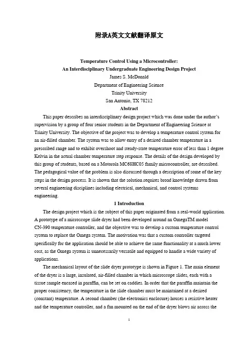
附录A英文文献翻译原文Temperature Control Using a Microcontroller:An Interdisciplinary Undergraduate Engineering Design ProjectJames S. McDonaldDepartment of Engineering ScienceTrinity UniversitySan Antonio, TX 78212AbstractThis paper describes an interdisc iplinary design project which was done under the author’s supervision by a group of four senior students in the Department of Engineering Science at Trinity University. The objective of the project was to develop a temperature control system for an air-filled chamber. The system was to allow entry of a desired chamber temperature in a prescribed range and to exhibit overshoot and steady-state temperature error of less than 1 degree Kelvin in the actual chamber temperature step response. The details of the design developed by this group of students, based on a Motorola MC68HC05 family microcontroller, are described. The pedagogical value of the problem is also discussed through a description of some of the key steps in the design process. It is shown that the solution requires broad knowledge drawn from several engineering disciplines including electrical, mechanical, and control systems engineering.1 IntroductionThe design project which is the subject of this paper originated from a real-world application.A prototype of a microscope slide dryer had been developed around an OmegaTM modelCN-390 temperature controller, and the objective was to develop a custom temperature control system to replace the Omega system. The motivation was that a custom controller targeted specifically for the application should be able to achieve the same functionality at a much lower cost, as the Omega system is unnecessarily versatile and equipped to handle a wide variety of applications.The mechanical layout of the slide dryer prototype is shown in Figure 1. The main element of the dryer is a large, insulated, air-filled chamber in which microscope slides, each with a tissue sample encased in paraffin, can be set on caddies. In order that the paraffin maintain the proper consistency, the temperature in the slide chamber must be maintained at a desired (constant) temperature. A second chamber (the electronics enclosure) houses a resistive heater and the temperature controller, and a fan mounted on the end of the dryer blows air across theheater, carrying heat into the slide chamber. This design project was carried out during academic year 1996–97 by four students under the author’s supervision as a Senior Design project in the Department of Engineering Science at Trinity University. The purpose of this paper isto describe the problem and the students’ solution in some detail, and to discuss some of the pedagogical opportunities offered by an interdisciplinary design project of this type. The students’ own report was presented a t the 1997 National Conference on Undergraduate Research [1]. Section 2 gives a more detailed statement of the problem, including performance specifications, and Section 3 describes the students’ design. Section 4 makes up the bulk of the paper, and discusses in some detail several aspects of the design process which offer unique pedagogical opportunities. Finally, Section 5 offers some conclusions.2 Problem StatementThe basic idea of the project is to replace the relevant parts of the functionality of an Omega CN-390 temperature controller using a custom-designed system. The application dictates that temperature settings are usually kept constant for long periods of time, but it’s nonetheless important that step changes be tracked in a “reasonable” manner. Thus the main requirements boil down to·allowing a chamber temperature set-point to be entered,·displaying both set-point and actual temperatures, and·tracking step changes in set-point temperature with acceptable rise time, steady-state error, and overshoot.Although not explicitly a part of the specifications in Table 1, it was clear that the customer desired digital displays of set-point and actual temperatures, and that set-point temperature entry should be digital as well (as opposed to, say, through a potentiometer setting).3 System DesignThe requirements for digital temperature displays and setpoint entry alone are enough to dictate that a microcontrollerbased design is likely the most appropriate. Figure 2 shows a block diagram of the stude nts’ design.The microcontroller, a MotorolaMC68HC705B16 (6805 for short), is the heart of the system. It accepts inputs from a simple four-key keypad which allow specification of the set-point temperature, and it displays both set-point and measured chamber temperatures using two-digit seven-segment LED displays controlled by a display driver. All these inputs and outputs are accommodated by parallel ports on the 6805. Chamber temperature is sensed using apre-calibrated thermistor and input via one of the 6805’s analog-to-digital inputs. Finally, a pulse-width modulation (PWM) output on the 6805 is used to drive a relay which switches line power to the resistive heater off and on.Figure 3 shows a more detailed schematic of the electronics and their interfacing to the 6805. The keypad, a Storm 3K041103, has four keys which are interfaced to pins PA0{ PA3 of Port A, configured as inputs. One key functions as a mode switch. Two modes are supported: set mode and run mode. In set mode two of the other keys are used to specify the set-point temperature: one increments it and one decrements. The fourth key is unused at present. The LED displays are driven by a Harris Semiconductor ICM7212 display driver interfaced to pins PB0{PB6 of Port B, configured as outputs. The temperature-sensing thermistor drives, through a voltage divider, pin AN0 (one of eight analog inputs). Finally, pin PLMA (one of two PWM outputs) drives the heater relay.Software on the 6805 implements the temperature control algorithm, maintains the temperature displays, and alters the set-point in response to keypad inputs. Because it is not complete at this writing, software will not be discussed in detail in this paper. The control algorithm in particular has not been determined, but it is likely to be a simple proportional controller and certainly not more complex than a PID. Some control design issues will be discussed in Section 4, however.4 The Design ProcessAlthough essentially the project is just to build a thermostat, it presents many nice pedagogical opportunities. The knowledge and experience base of a senior engineering undergraduate are just enough to bring him or her to the brink of a solution to various aspects of the problem. Yet, in each case, realworld considerations complicate the situation significantly.Fortunately these complications are not insurmountable, and the result is a very beneficial design experience. The remainder of this section looks at a few aspects of the problem which present the type of learning opportunity just described. Section 4.1 discusses some of the features of a simplified mathematical model of the thermal properties of the system and how it can beeasily validated experimentally. Section 4.2 describes how realistic control algorithm designs can be arrived at using introductory concepts in control design. Section 4.3 points out some important deficiencies of such a simplified modeling/control design process and how they can be overcome through simulation. Finally, Section 4.4 gives an overview of some of the microcontroller-related design issues which arise and learning opportunities offered.4.1 MathematicalModelLumped-element thermal systems are described in almost any introductory linear control systems text, and just this sort of model is applicable to the slide dryer problem. Figure 4 shows a second-order lumped-element thermal model of the slide dryer. The state variables are the temperatures Ta of the air in the box and Tb of the box itself. The inputs to the system are the power output q(t) of the heater and the ambient temperature T¥. ma and mb are the masses of the air and the box, respectively, and Ca and Cb their specific heats. μ1 and μ2 are heat transfer coefficients from the air to the box and from the box to the external world, respectively.It’s not hard to show that the (linearized) state equationscorresponding to Figure 4 areTaking Laplace transforms of (1) and (2) and solving for Ta(s), which is the output of interest, gives the following open-loop model of the thermal system:where K is a constant and D(s) is a second-order polynomial.K, tz, and the coefficients ofD(s) are functions of the variousparameters appearing in (1) and (2).Of course the various parameters in (1) and (2) are completely unknown, but it’s not hard to show that, regardless of their values, D(s) has two real zeros. Therefore the main transfer function of interest (which isthe one from Q(s), since we’ll assume constant ambient temperature) can be writtenMoreover, it’s not too hard to show that 1=tp1 <1=tz <1=tp2, i.e., that the zero lies between the two poles. Both of these are excellent exercises for the student, and the result is the openloop pole-zero diagram of Figure 5.Obtaining a complete thermal model, then, is reduced to identifying the constant K and the three unknown time constants in (3). Four unknown parameters is quite a few, but simple experiments show that 1=tp1 _ 1=tz;1=tp2 so that tz;tp2 _ 0 are good approximations. Thus the open-loop system is essentially first-order and can therefore be written(where the subscript p1 has been dropped).Simple open-loop step response experiments show that,for a wide range of initial temperatures and heat inputs, K _0:14 _=W and t _ 295 s.14.2 Control System DesignUsing the first-order model of (4) for the open-loop transfer function Gaq(s) and assuming for the moment that linear control of the heater power output q(t) is possible, the block diagram of Figure 6 represents the closed-loop system. Td(s) is the desired, or set-point, temperature,C(s) is the compensator transfer function, and Q(s) is the heater output in watts.Given this simple situation, introductory linear control design tools such as the root locus method can be used to arrive at a C(s) which meets the step response requirements on rise time, steady-state error, and overshoot specified in Table 1. The upshot, of course, is that a proportional controller with sufficient gain can meet all specifications. Overshoot is impossible, and increasing gains decreases both steady-state error and rise time.Unfortunately, sufficient gain to meet the specifications may require larger heat outputs than the heater is capable of producing. This was indeed the case for this system, and the result is that the rise time specification cannot be met. It is quite revealing to the student how useful such an oversimplified model, carefully arrived at, can be in determining overall performance limitations.4.3 Simulation ModelGross performance and its limitations can be determined using the simplified model of Figure 6, but there are a number of other aspects of the closed-loop system whose effects on performance are not so simply modeled. Chief among these are·quantization error in analog-to-digital conversion of the measured temperature and· the use of PWM to control the heater.Both of these are nonlinear and time-varying effects, and the only practical way to study them is through simulation (or experiment, of course).Figure 7 shows a SimulinkTM block diagram of the closed-loop system which incorporates these effects. A/D converter quantization and saturation are modeled using standard Simulink quantizer and saturation blocks. Modeling PWM is more complicated and requires a customS-function to represent it.This simulation model has proven particularly useful in gauging the effects of varying thebasic PWM parameters and hence selecting them appropriately. (I.e., the longer the period, the larger the temperature error PWM introduces. On the other hand, a long period is desirable to avoid excessiv e relay “chatter,” among other things.) PWM is often difficult for students to grasp, and the simulation model allows an exploration of its operation and effects which is quite revealing.4.4 The MicrocontrollerSimple closed-loop control, keypad reading, and display control are some of the classic applications of microcontrollers, and this project incorporates all three. It is therefore an excellent all-around exercise in microcontroller applications. In addition, because the project isto produce an actua l packaged prototype, it won’t do to use a simple evaluation board with theI/O pins jumpered to the target system. Instead, it’s necessary to develop a complete embedded application. This entails the choice of an appropriate part from the broad range offered in a typical microcontroller family and learning to use a fairly sophisticated development environment. Finally, a custom printed-circuit board for the microcontroller and peripherals must be designed and fabricated.Microcontroller Selection. In view of existing local expertise, the Motorola line of microcontrollers was chosen for this project. Still, this does not narrow the choice down much. A fairly disciplined study of system requirements is necessary to specify which microcontroller, out of scores of variants, is required for the job. This is difficult for students, as they generally lack the experience and intuition needed as well as the perseverance to wade through manufacturers’ selection guides.Part of the problem is in choosing methods for interfacing the various peripherals (e.g., what kind of display driver should be used?). A study of relevant Motorola application notes [2, 3, 4] proved very helpful in understandingwhat basic approaches are available, and what microcontroller/peripheral combinations should be considered.The MC68HC705B16 was finally chosen on the basis of its availableA/D inputs and PWMoutputs as well as 24 digital I/O lines. In retrospect this is probably overkill, as only oneA/D channel, one PWM channel, and 11 I/O pins are actually required (see Figure 3). The decision was made to err on the safe side because a complete development system specific to the chosen part was necessary, and the project budget did not permit a second such system to be purchased should the firstprove inadequate.Microcontroller Application Development. Breadboarding of the peripheral hardware, development of microcontroller software, and final debugging and testing of a customprinted-circuit board for the microcontroller and peripherals all require a development environment of some kind. The choice of a development environment, like that of themicrocontroller itself, can be bewildering and requires some faculty expertise. Motorola makes three grades of development environment ranging from simple evaluation boards (at around $100) to full-blown real-time in-circuit emulators (at more like $7500). The middle option was chosen for this project: the MMEVS, which consists of _ a platform board (which supports all 6805-family parts), _ an emulator module (specific to B-series parts), and _ a cable and target head adapter (package-specific). Overall, the system costs about $900 and provides, with some limitations, in-circuit emulation capability. It also comes with the simple but sufficient software development environment RAPID [5].Students find learning to use this type of system challenging, but the experience they gain in real-world microcontroller application development greatly exceeds the typical first-course experience using simple evaluation boards.Printed-Circuit Board. The layout of a simple (though definitely not trivial) printed-circuit board is another practical learning opportunity presented by this project. The final board layout, with package outlines, is shown (at 50% of actual size) in Figure 8. The relative simplicity of the circuit makes manual placement and routing practical—in fact, it likely gives better results than automatic in an application like this—and the student is therefore exposed to fundamental issues of printed-circuit layout and basic design rules. The layout software used was the very nice package pcb,2 and the board was fabricated in-house with the aid of our staff electronics technician.5 ConclusionThe aim of this paper has been to describe an interdisciplinary, undergraduate engineering design project: a microcontroller- based temperature control system with digital set-point entry and set-point/actual temperature display. A particular design of such a system has been described, and a number of design issues which arise—from a variety of engineering disciplines—have been discussed. Resolution of these issues generally requires knowledge beyond that acquired in introductory courses, but realistically accessible to advance undergraduate students, especiallywith the advice and supervision of faculty.Desirable features of the problem, from a pedagogical viewpoint, include the use of a microcontroller with simple peripherals, the opportunity to usefully apply introductorylevel modeling of physical systems and design of closed-loop controls, and the need for relatively simple experimentation (for model validation) and simulation (for detailed performance prediction). Also desirable are some of the technologyrelated aspects of the problem including practical use of resistive heaters and temperature sensors (requiring knowledge of PWM and calibration techniques, respectively), microcontroller selection and use of development systems, and printedcircuit design.AcknowledgementsThe author would like to acknowledge the hard work, dedication, and ability shown by the students involved in this project: Mark Langsdorf, Matt Rall, PamRinehart, and David Schuchmann. It is their project, and credit for its success belongs to them.References[1] M. Langsdorf, M. Rall, D. Schuchmann, and P. Rinehart,“Temperature control of a microscope slide dryer,” in1997 National Conference on Undergraduate Research,(Austin, TX), April 1997. Poster presentation.[2] Motorola, Inc., Phoenix, AZ, Temperature Measurementand Display Using the MC68HC05B4 and the MC14489,1990. Motorola SemiconductorApplicationNote AN431.[3] Motorola, Inc., Phoenix, AZ, HC05 MCU LED DriveTechniques Using the MC68HC705J1A, 1995. MotorolaSemiconductor Application Note AN1238.[4] Motorola, Inc., Phoenix, AZ, HC05MCU Keypad DecodingTechniques Using the MC68HC705J1A, 1995. MotorolaSemiconductor Application Note AN1239.[5] Motorola, Inc., Phoenix, AZ, RAPID Integrated DevelopmentEnvironment User’s Manual, 1993. (RAPID wasdeveloped by P & E Microcomputer Systems, Inc.).附录B英文文献翻译中文单片机温度控制:一个跨学科的本科生工程设计项目JamesS.McDonald工程科学系三一大学德克萨斯州圣安东尼奥市78212摘要本文所描述的是作者领导由四个三一大学高年级学生组成的团队进行的一个跨学科工程项目的设计。
自动化专业 单片机相关 外文文献 英文文献 外文翻译中英对照
本科生毕业论文(外文翻译) 译文名称:MCS -51 系列单片机的功能和结构专业:自动化班次:学员:指导教员:评阅人:完成时间:2022 年11 月30 日Structure and function of the MCS-51 series Structure and function of the MCS-51 series one-chip computer is a name ofa piece of one-chip computer series which Intel Company produces. This company introduced 8 top-grade one-chip computers of MCS-51 series in 1980 after introducing 8 one-chip computers of MCS-48 series in 1976. It belong to alot of kinds this line of one-chip computer the chips have,such as 8051, 8031, 8751, 80C51BH, 80C31BH,etc., their basic composition, basic performance and instruction system are all the same. 8051 daily representatives- 51 serial one-chip computers .An one-chip computer system is made up of several following parts: ( 1) One microprocessor of 8 (CPU). ( 2) At slice data memory RAM (128B/256B),it use not depositting not can reading /data that write, such as result not middle of operation, final result and data wanted to show, etc. ( 3) Procedure memory ROM/EPROM (4KB/8KB ), is used to preserve the procedure , some initial data and form in slice. But does not take ROM/EPROM within some one-chip computers, such as 8031 , 8032, 80C ,etc.. ( 4) Four 8 run side by side I/O interface P0 four P3, each mouth can use as introduction , may use as exporting too. ( 5) Two timer / counter, each timer / counter may set up and count in the way, used to count to the external incident, can set up into a timing way too, and can according to count or result of timing realize the control of the computer. ( 6) Five cut off cutting off the control system of the source . ( 7) One all duplexing serial I/O mouth of UART (universal asynchronous receiver/transmitter (UART) ), is it realize one-chip computer or one-chip computer and serial communication of computer to use for. ( 8) Stretch oscillator and clock produce circuit, quartz crystal finely tune electric capacity need outer. Allow oscillation frequency as 12 megahertas now at most. Every the above-mentioned part was joined through the inside data bus .Among them, CPU is a core of the one-chip computer, it is the control of the computer and command centre, made up of such parts as arithmetic unit and controller , etc.. The arithmetic unit can carryon 8 persons of arithmetic operation and unit ALU of logic operation while including one, the 1 storing device temporarilies of 8, storing device 2 temporarily, 8's accumulation device ACC, register B and procedure state register PSW, etc. Person who accumulate ACC count by 2 input ends entered of checking etc. temporarily as one operation often, come from person who store 1 operation is it is it make operation to go on to count temporarily , operation result and loopback ACC with another one. In addition, ACC is often regarded as the transfer station of data transmission on 8051 inside . The same as general microprocessor, it is the busiest register. Help remembering that agreeing with A expresses in the order. The controller includes the procedure counter , the order is depositted, the order decipher, the oscillator and timing circuit, etc. The procedure counter is made up of counter of 8 for two, amounts to 16. It is a byte address counter of the procedure in fact, the content is the next IA that will carried out in PC. The content which changes it can change the direction that the procedure carries out . Shake the circuit in 8051 one-chip computers, only need outer quartz crystal and frequency to finely tune the electric capacity, its frequency range is its 12MHZ of 1.2MHZ. This pulse signal, as 8051 basic beats of working, namely the minimum unit of time. 8051 is the same as other computers, the work in harmony under the control of the basic beat, just like an orchestra according to the beat play that is commanded.There are ROM (procedure memory , can only read ) and RAM in 8051 slices (data memory, can is it can write ) two to read, they have each independent memory address space, dispose way to be the same with general memory of computer. Procedure 8051 memory and 8751 slice procedure memory capacity 4KB, address begin from 0000H, used for preserving the procedure and form constant. Data 8051- 8751 8031 of memory data memory 128B, address false 00FH, use for middle result to deposit operation, the data are stored temporarily and the data are buffered etc.. In RAM of this 128B, there is unit of 32 byteses that can be appointed as the job register, this and generalmicroprocessor is different, 8051 slice RAM and job register rank one formation the same to arrange the location. It is not very the same that the memory of MCS-51 series one-chip computer and general computer disposes the way in addition. General computer for first address space, ROM and RAM can arrangein different space within the range of this address at will, namely the addressesof ROM and RAM, with distributing different address space in a formation. While visiting the memory, corresponding and only an address Memory unit, can ROM, it can be RAM too, and by visiting the order similarly. This kind of memory structure is called the structure of Princeton. 8051 memories are divided into procedure memory space and data memory space on the physics structure, there are four memory spaces in all: The procedure stores in one and data memory space outside data memory and one in procedure memory space and one outside one, the structure forms of this kind of procedure device and data memory separated form data memory, called Harvard structure. But use the angle from users, 8051 memory address space is divided into three kinds: (1) In the slice, arrange blocks of FFFFH , 0000H of location , in unison outside the slice (use 16 addresses). (2) The data memory address space outside one of 64KB, the address is arranged from 0000H 64KB FFFFH (with 16 addresses ) too to the location. (3) Data memory address space of 256B (use 8 addresses). Three above-mentioned memory space addresses overlap, for distinguishing and designing the order symbol of different data transmission in the instruction system of 8051: CPU visit slice, ROM order spend MOVC , visit block RAM order uses MOVX outside the slice, RAM order uses MOV to visit in slice.8051 one-chip computer have four 8 walk abreast I/O port, call P0, P1, P2 and P3. Each port is 8 accurate two-way mouths, accounts for 32 pins altogether. Every one I/O line can be used as introduction and exported independently. Each port includes a latch (namely special function register ), one exports the driver and a introduction buffer . Make data can latch when outputting, data can buffer when making introduction , but four function of passway these self-same.Expand among the system of memory outside having slice, four port these may serve as accurate two-way mouth of I/O in common use. Expand among the system of memory outside having slice, P2 mouth see high 8 address off; P0 mouth is a two-way bus, send the introduction of 8 low addresses and data / export in timesharingThe circuit of 8051 one-chip computers and four I/O ports is very ingenious in design. Familiar with I/O port logical circuit, not only help to use ports correctly and rationally, and will inspire to designing the peripheral logical circuit of one-chip computer to some extent. Load ability and interface of port have certain requirement, because output grade, P0 of mouth and P1 end output, P3 of mouth grade different at structure, so, the load ability and interface of its door demand to have nothing in common with each other. P0 mouth is different from other mouths, its output grade draws the resistance supremly. When using it as the mouth in common use to use, output grade is it leak circuit to turn on, is it is it urge NMOS draw the resistance on taking to be outer with it while inputting toEvery one with P0 mouth can drive 8 Model LS TTL load to export. P1 mouth is an accurate two-way mouth too, used as I/O in common use. Different from P0 mouth output of circuit its, draw load resistance link with power on inside have. In fact, the resistance is that two effects are in charge of FET and together: One FET is in charge of load, its resistance is regular. Another one can is it lead to work with close at two state, make its President resistance value change approximate 0 or group value heavy two situation very. When it is 0 that the resistance is approximate , can draw the pin to the high level fast ; When resistance value is very large, P1 mouth, in order to hinder the introduction state high. Output as P1 mouth high electricity at ordinary times, can is it draw electric current load to offer outwards, draw the resistance on needn't answer and thenning. Here when the port is used as introduction, must write into 1 to the corresponding latch first too, make FET end. Relatively about 20,000 ohmsbecause of the load resistance in scene and because 40,000 ohms, will not exert an influence on the data that are input. The structure of P2 some mouth is similar to P0 mouth, there are MUX switches. Is it similar to mouth partly to urge, but mouth large a conversion controls some than P1. P3 mouth one multi-functionalthese, make her besides accurate two-way function with P1 mouth just, can alsodetermines to be to output data of latch to output second signal of function. Act as W =At 1 o'clock, output Q end signal; Act as Q =At 1 o'clock, can output W line signal . At the time of programming, it is that the first function is still the second function but needn't have software that set up P3 mouth in advance . It hardware not inside is the automatic to have two function outputted when CPU carries on SFR and seeks the location (the location or the byte ) to visit to P3 mouth /at not lasting lining, there are inside hardware latch Qs =1.The operation principle of P3 mouth is similar to P1 mouth.Output grade , P3 of mouth , P1 of P1 , connect with inside have load resistance of drawing , every one of they can drive 4 Model LS TTL load to output. As while inputting the mouth, any TTL or NMOS circuit can drive P1 of 8051 one-chip computers as P3 mouth in a normal way . Because draw resistance on output grade of them have, can open a way collector too or drain-source resistance is it urge to open a way, do not need to have the resistance of drawing outerly . Mouths are all accurate two-way mouths too. When the conduct is input, must write the corresponding port latch with 1 first . As to 80C51 one-chip computer, port can only offer milliampere of output electric currents, is it output mouth go when urging one ordinary basing of transistor to regard as, should contact a resistance among the port and transistor base , in order to the electricity while restraining the high level from exporting P1~P3 Being restored to the throne is the operation of initializing of an one-chip computer. Its main function is to turn PC into 0000H initially , make theone-chip computer begin to hold the conduct procedure from unit 0000H. Except that the ones that enter the system are initialized normally,as because procedure operate it make mistakes or operate there aren't mistake, in order to extricate oneself from a predicament , need to be pressed and restored to the throne the key restarting too. It is an input end which is restored to the throne the signal in 8051 China RST pin. Restore to the throne signal high level effective , should sustain 24 shake cycle (namely 2 machine cycles ) the above its effective times. If 6 of frequency of utilization brilliant to shake, restore to the throne signal duration should exceed 4 delicate to finish restoring to the throne and operating. Produce the logic picture of circuit which is restored to the throne the signal:Restore to the throne the circuit and include two parts outside in the chip entirely. Outside that circuit produce to restore to the throne signal (RST ) hand over to Schmitt's trigger, restore to the throne circuit sample to output , Schmitt of trigger constantly in each S5P2 , machine of cycle in having one more , then just got and restored to the throne and operated the necessary signal insidly. Restore to the throne resistance of circuit generally, electric capacity parameter suitable for 6 brilliant to shake, can is it restore to the throne signal high level duration greater than 2 machine cycles to guarantee. Being restored to the throne in the circuit is simple, its function is very important. Pieces of one-chip computer system could normal running,should first check it can restore to the throne not succeeding. Checking and can pop one's head and monitor the pin with the oscillograph tentatively, push and is restored to the throne the key, the wave form that observes and has enough range is exported (instantaneous), can also through is it restore to the throne circuit group holding value carry on the experiment to change.MCS -51 系列单片机的功能和结构MCS - 51 系列单片机具有一个单芯片电脑的结构和功能,它是英特尔公司生产的系列产品的名称。
单片机外文文献翻译(2024)
引言:单片机(Microcontroller)是一种广泛应用于嵌入式系统中的小型计算机芯片。
它集成了处理器核心、存储器、外设接口和时钟电路等核心部件,可以独立运行。
随着全球化的发展,外文文献对于学习和研究单片机领域来说至关重要。
本文翻译的外文文献《MicrocontrollerbasedTrafficLightControlSystem》详细介绍了基于单片机的交通信号灯控制系统。
概述:交通信号灯控制是现代都市交通系统中至关重要的一环。
传统的交通信号灯控制系统通常由定时器控制,不能根据实际交通情况动态调整信号灯的时间。
而基于单片机的交通信号灯控制系统可以实现根据实时交通流量来动态调整信号灯的时间,优化交通效率。
本文将详细介绍该系统的设计和实现。
正文:一、单片机选型1.1.CPU性能:本文选择了一款高性能的32位单片机作为控制核心,它具有较高的处理能力和较大的存储器容量,可以同时处理多条交通路口的信号控制。
1.2.外设接口:该单片机具有丰富的外设接口,可以与交通信号灯、传感器和通信设备等进行连接,实现信号控制和数据交互。
1.3.低功耗设计:为了节约能源和延长系统寿命,在单片机选型时考虑了低功耗设计,降低系统运行的能耗。
二、硬件设计2.1.交通信号灯:在设计交通信号灯时,考虑了日夜可见性和能耗。
采用了高亮度LED作为信号灯光源,同时添加了光敏传感器控制信号灯的亮度,以满足不同时间段的亮度需求。
2.2.传感器:通过安装车辆感应器和行人感应器等传感器,可以在实时监测交通流量的基础上,智能调整信号灯时间,提高路口的交通效率。
2.3.通信设备:在交通信号灯控制系统中引入了通信设备,可以实现各交通路口之间的信息交互和协调控制,提高整体交通系统的效率。
三、软件设计3.1.程序架构:采用了多任务的实时操作系统,将交通信号灯控制、传感器数据处理和通信设备控制等功能分别封装成不同的任务,实现了系统的高效运行和任务调度。
单片机设计外文文献翻译(含中英文)
附录A 外文翻译——AT89S52/AT89S51技术手册AT89S52译文主要性能与MCS-51单片机产品兼容8K字节在系统可编程Flash存储器1000次擦写周期全静态操作:0Hz~33Hz三级加密程序存储器32个可编程I/O口线三个16位定时器/计数器八个中断源全双工UART串行通道低功耗空闲和掉电模式掉电后中断可唤醒看门狗定时器双数据指针掉电标识符功能特性描述AT89S52是一种低功耗、高性能CMOS8位微控制器,具有8K在系统可编程Flash 存储器。
使用Atmel公司高密度非易失性存储器技术制造,与工业80C51产品指令和引脚完全兼容。
片上Flash 允许程序存储器在系统可编程,亦适于常规编程器。
在单芯片上,拥有灵巧的8位CPU和在系统可编程Flash,使得AT89S52为众多嵌入式控制应用系统提供高灵活、超有效的解决方案。
AT89S52具有以下标准功能:8k字节Flash,256字节RAM,32位I/O口线,看门狗定时器,2个数据指针,三个16位定时器/计数器,一个6向量2级中断结构,全双工串行口,片内晶振及时钟电路。
另外,AT89S52可降至0Hz静态逻辑操作,支持2种软件可选择节电模式。
空闲模式下,CPU停止工作,允许RAM、定时器/计数器、串口、中断继续工作。
掉电保护方式下,RAM内容被保存,振荡器被冻结,单片机一切工作停止,直到下一个中断或硬件复位为止。
引脚结构方框图VCC : 电源GND :地P0口:P0口是一个8位漏极开路的双向I/O口。
作为输出口,每位能驱动8个TTL逻辑电平。
对P0端口写“1”时,引脚用作高阻抗输入。
当访问外部程序和数据存储器时,P0口也被作为低8位地址/数据复用。
在这种模式下,P0具有内部上拉电阻。
在flash编程时,P0口也用来接收指令字节;在程序校验时,输出指令字节。
程序校验时,需要外部上拉电阻。
P1口:P1 口是一个具有内部上拉电阻的8位双向I/O 口,p1 输出缓冲器能驱动4个TTL 逻辑电平。
电气自动化 单片机 外文文献 英文文献 外文翻译 中英对照
Single-chip1.The definition of a single-chipSingle-chip is an integrated on a single chip a complete computer system .Even though most of his features in a small chip,but it has a need to complete the majority of computer components:CPU,memory,internal and external bus system,most will have the Core.At the same time,such as integrated communication interfaces,timers,real-time clock and other peripheral equipment.And now the most powerful single-chip microcomputer system can even voice ,image,networking,input and output complex system integration on a single chip.Also known as single-chip MCU(Microcontroller),because it was first used in the field of industrial control.Only by the single-chip CPU chip developed from the dedicated processor. The design concept is the first by a large numberof peripherals and CPU in a single chip,the computer system so that smaller,more easily integrated into the complex and demanding on the volume control devices.INTEL the Z80 is one of the first design in accordance with the idea of the processor,From then on,the MCU and the development of a dedicated processor parted ways.Early single-chip 8-bit or all the four.One of the most successful is INTELs 8031,because the performance of a simple and reliable access to a lot of good praise.Since then in 8031to develop a single-chip microcomputer system MCS51 series.based on single-chip microcomputer system of the system is still widely used until now.As the field of industrial control requirements increase in the beginning of a 16-bit single-chip,but not ideal because the price has not been very widely used.After the90s with the big consumer electronics product development,single-chip technology is a huge improvement.INTEL i960 series with subsequent ARM in particular ,a broad range of application,quickly replaced by 32-bit single-chip 16-bit single-chip performance has been the rapid increase in processing power compared to the 80s to raise a few hundred times.At present,the high-end 32-bit single-chip frequency over 300MHz,the performance of the mid-90s close on the heels of a special processor,while the ordinary price of the model dropped to one U.S dollars,the most high-end models,only 10 U.S dollars.Contemporary single-chip microcomputer system is no longer only the bare-metal environment in the development and use of a large number of dedicated embedded operating system is widely used in the full range of single-chip microcomputer.In PDAs and cellphones as the coreprocessing of high-end single-chip or even a dedicated direct access to Windows and Linux operating systems.More than a dedicated single-chip processor suitable for embedded systems,so it was up to the application.In fact the number of single-chip is the worlds largest computer.Modern human life used in almost every piece of electronic and mechanical products will have a single-chip integration.Phone,telephone,calculator,home applicances,electronic toys,handheld computers and computer accessories such as a mouse in the Department are equipped with 1-2 single chip.And personal computers also have a large number of single-chip microcomputer in the workplace.Vehicles equipped with more than 40 Department of the general single-chip ,complex industrial control systems and even single-chip may have hundreds of work at the same time!SCM is not only far exceeds the number of PC and other integrated computing,even more than the number of human beings.2.single-chip introducedSingle-chip,also known as single-chip microcontroller,it is not the completion of a logic function of the chip,but a computer system integrated into a chip.Speaking in general terms: a single chip has become a computer .Its small size,light weight,cheap,for the learning,application and development of facilities provided .At the same time,learning to use the principle of single-chip computer to understand and structure the best choice.Single-chip and computer use is also similar to the module,such as CPU,memory,parallel bus, as well as the role and the same hard memory,is it different from the performance of these components are relatively weak in our home computer a lot,but the price is low ,there is generally no more than 10yuan,,can use it to make some control for a class of electrical work is not very complex is sufficient.We are using automatic drum washing machines, smoke hood,VCD and so on inside the home appliances can see its shadow! It is mainly as part of the core components of the control.It is an online real-time control computer,control-line is at the scene,we need to have a stronger anti-interference ability,low cost,and this is off-line computer(such as home PC)The main difference.By single-chip process,and can be amended.Through different procedures to achieve different functions,in particular the special unique features,this is the need to charge other devices can do a great effort,some of it is also difficult to make great efforts to do so .A function is not very complicated fi the United States the development of the 50s series of 74 or 60 during the CD4000series to get these pure hardware,the circuit must be a big PCB board !However,if the United States if the successful 70s seriesof single-chip market ,the result will be different!Simply because the adoption of single-chip preparation process you can achieve high intelligence,high efficiency and high reliability!Because of cost of single-chip is sensitive,so the dominant software or the lowest level assembly language,which is in addition to the lowest level for more than binary machine code of the language ,since such a low-level so why should we use ?Many of the seniors language has reached a level of visual programming why is it not in use ?The reason is simple ,that is,single-chip computer as there is no home of CPU,also not as hard as the mass storage device.A visualization of small high-level language program,even if there is only one button which will reach the size of dozens of K! For the home PCs hard drive is nothing,but in terms of the single-chip microcomputer is unacceptable.Single-chip in the utilization of hardware resources have to do very high ,so the compilation of the original while still in heavy use .The same token ,if the computer giants operating system and appplications run up to get the home PC,homePCcan not afford to sustain the same.It can be said that the twentieth century across the three “power”of the times,that is ,the electrical era,the electronic age and has now entered the computer age. However ,such a computer,usually refers to a personal computer,or PC.It consisits of the host ,keyboards,displays .And other components.There is also a type of computer,not how most people are familiar with . This computer is smart to give a variety of mechanical single-chip(also known as micro-controller).As the name suggests,these computer systems use only the minimum of an integrated circuit to make a simple calculation and control. Because of its small size,are usually charged with possession of machine in the “belly”in. It in the device,like the human mind plays a role, it is wrong,the entire device was paralyzed .Now,this single chip has a very wide field of use,such as smart meters,real-time industrial control,communications equipment,navigation systems,and household appliances. Once a variety of products with the use of the single-chip ,will be able to play so that the effectiveness of product upgrading,product names often adjective before the word “intelligent”,such as was hing machines and so intelligent.At present,some technical personnel of factories or other amateur electrtonics developers from engaging in certain products ,not the circuit is too complex ,that is functional and easy to be too simple imitation.The reason may be the product not on the cards or the use of single-chip programmable logic device on the other.3.single-chip historysingle-chip 70 was born in the late 20th century,experienced a SCM,MCU,SOC three stages.Single-chip micro-computer 1.SCM that(Single Chip Microcomputer)stage,is mainly a single from to find the best of the best embedded systems architecture.”Innovation model”to be successful,lay the SCM with the general-purpose computers,a completely different path of development . In embedded systems to create an independent development path,Intel Corporation credit.That is 2.MCU microcontroller(Micro Controller Unit)stage,the main direction of technology development: expanding to meet the embedded applications,the target system requirements for the various peripheral circuits and interface circuits,to highlingt the target of intelligent control.It covers all areas related with the objectSystem,therefore,the development of MCU inevitably fall on the heavy electrical,electronics manufacturers. From this point of view ,Intels development gradually MCU has its objective factors.MCU in the development ,the most famous manufacturers when the number of Philips Corporation.Philips in embedded applications for its enormous advantages,the MCS-51 from the rapid deveploment of single-chip micro-computer to the microcontroller.Therefore,when we look back at the path of development of embedded systems,Intel and Philips do not forget the historical merits.3.Single-chip is an independent embedded systems development,to the MCU an important factor in the development stage,is seeking applications to maximize the natural trend .With the mico-electronics technology,IC design,EDA tools development,based on the single-chip SOC design application systems will have greater development. Therefore,the understanding of single-chip micro-computer from a single ,monolithic single-chip microcontroller extends to applications.4.Single-chip applicationsAt present,single-chip microcomputer to infiltrate all areas of our lives,which is very difficult to find the area of almost no traces of single-chip microcomputer.Missile navigation equipment,aircraft control on a variety of instruments,compuer network communications and data transmission,industrial automation,real-time process control and data processing ,are widely used in a variety of smart IC card,limousine civilian security systems,video recorders,cameras,the control of automatic washing machines,as well as program-controllde toys,electronic pet,etc,which are inseparable from the single-chip microcomputer.Not to mention the field of robot automation ,intelligent instrumentation,medical equipment has been. Therefore,the single- chip learning ,development and application to a large number of computer applications and intelligent control of scientists,engineers.Single-chip widely used in instruments and meters,household appliances,medical equipment ,acrospace,specialized equipment and the intellingent management in areas such as process control,generally can be divided into the following areas:1.In the smart application of instrumentationSingle-chip with small size,low power consumption,control,and expansion flexibility , miniaturization and ease of sensors,can be realized,suchvoltage,power,frequency,humidity,temperature,flow,speed,thickness,angle,length,hardness,elemen t,measurement of physical pressure. SCM makes use of digital instrumentation,intelligence,miniaturization and functional than the use of electronic or digital circuitry even stronger.For example,precision measurement equipment(power meter,oscilloscope,and analyzer).2.In the industrial controlMCU can constitute a variety of control systems,data acquisition system.Such as factory assembly line of intelligent management ,intelligent control of the lift ,all kinds of alarm systems ,and computer networks constitute a secondary control system.3.In the applicationof household appliancesIt can be said that almost all home appliances are using the single-chip control,electric rice from favorable,washing machines,refrigerators,air conditioners,color TV and other audio video equipment,and then to the electronic weighing equipment,all kinds ,everywhere.4.On computer networks and communication applications in the field ofGenerally with the modern single-chip communication interface,can be easily carried out with computer carried out with computer data communications,computer networks and in inter-application communications equipment to provide an excellent material conditions,the communications equipment to provide an excellent material condition,from the mobile phone ,telephone , mini-program-controlled switchboards,buiding automated communications system call,the train wireless communications,and then you can see day-to-day work of mobile phones,Mobile communications,such as radios.5.Single-chip in the field of medical equipment applicationsSingle-chip microcomputer in medical devices have a wide range of purpose,such as medical ventilator,various analyzers,monitors,ultrasonic diagnostic equipment and hospital call systems.6.In a variety of large-scale electrical applications of modularSome special single-chip design to achieve a specific function to carry out a variety of modular circuitapplications,without requiring users to understand its internal structure.Integrated single-chip microcomputer such as music ,which seems to be simpleFunctions,a miniature electronic chip in a pure(as distinct from the principle of tape machine),would require a complex similar to the principle of the computer. Such as :music signal to digital form stored in memory(similar to ROM),read out by the microcontroller into analog music signal(similar to the sound card).In large circuits,modular applications that greatly reduces the size ,simplifying the circuit and reduce the damage,error rate ,but also to facilitate the replacement.In addition,single-chip microcomputer in the industrial,commercial,financial,scientific research ,education,defense aerospace and other fields have a wide range of uses.单片机1.单片机定义单片机是一种集成在电路芯片上的完整计算机系统。
基于单片机的外文翻译、中英文翻译
英文原文DescriptionThe at89s52 is a low-power, high-performance CMOS 8-bit microcomputer with 4K bytes of Flash Programmable and Erasable Read Only Memory (PEROM) and 128 bytes RAM. The device is manufactured using Atmel’s high density nonvolatile memory technology and is compatible with the industry standard MCS-51™ instruction set and pinout. The chip combines a versatile 8-bit CPU with Flash on a monolithic chip, the Atmel at89s52 is a powerful microcomputer which provides a highly flexible and cost effective solution to many embedded control applications.Features:• Compatible with MCS-51™ Products• 4K Bytes of In-System Reprogrammable Flash Memory• Endurance: 1,000 Write/Erase Cycles• Fully Static Operation: 0 Hz to 24 MHz• Three-Level Program Memory Lock• 128 x 8-Bit Internal RAM• 32 Programmable I/O Lines• Two 16-Bit Timer/Counters• Six Interrupt Sources• Programmable Serial Channel• Low Power Idle and Power Down ModesThe at89s52 provides the following standard features: 4K bytes of Flash, 128 bytes of RAM, 32 I/O lines, two 16-bit timer/counters, a five vector two-level interrupt architecture, a full duplex serial port, on-chip oscillator and clock circuitry. In addition, the at89s52 is designed with static logic for operation down to zero frequency and supports two software selectable power saving modes. The Idle Mode stops the CPU while allowing the RAM, timer/counters, serial port and interrupt system to continue functioning. The Power Down Mode saves the RAM contents but freezes the oscillator disabling all other chip functions until the next hardware reset. Pin Description:VCC Supply voltage.GND Ground.Port 0Port 0 is an 8-bit open drain bidirectional I/O port. As an output port each pin can sink eight TTL inputs. When is are written to port 0 pins, the pins can be used as high impedance inputs.Port 0 may also be configured to be the multiplexed loworder address/data bus during accesses to external program and data memory. In this mode P0 has internal pullups.Port 0 also receives the code bytes during Flash programming, and outputs theduring accesses to external memory. This pin is also the program pulse input (PROG) during Flash programming.In normal operation ALE is emitted at a constant rate of 1/6 the oscillator frequency, and may be used for external timing or clocking purposes. Note, however, that one ALE pulse is skipped during each access to external Data Memory.If desired, ALE operation can be disabled by setting bit 0 of SFR location 8EH. With the bit set, ALE is active only during a MOVX or MOVC instruction. Otherwise, the pin is weakly pulled high. Setting the ALE-disable bit has no effect if the microcontroller is in external execution mode.PSENProgram Store Enable is the read strobe to external program memory.When the at89s52 is executing code from external program memory, PSEN is activated twice each machine cycle, except that two PSEN activations are skipped during each access to external data memory.EA/VPPExternal Access Enable. EA must be strapped to GND in order to enable the device to fetch code from external program memory locations starting at 0000H up to FFFFH. Note, however, that if lock bit 1 is programmed, EA will be internally latched on reset.EA should be strapped to VCC for internal program executions.This pin also receives the 12-volt programming enable voltage(VPP) during Flash programming, for parts that require 12-volt VPP.XTAL1Input to the inverting oscillator amplifier and input to the internal clock operating circuit.XTAL2Output from the inverting oscillator amplifier.Oscillator CharacteristicsXTAL1 and XTAL2 are the input and output, respectively, of an inverting amplifier which can be configured for use as an on-chip oscillator, as shown in Figure 1. Either a quartz crystal or ceramic resonator may be used. To drive the device from an external clock source, XTAL2 should be left unconnected while XTAL1 is driven as shown in Figure 2. There are no requirements on the duty cycle of the external clock signal, since the input to the internal clocking circuitry is through adivide-by-two flip-flop, but minimum and maximum voltage high and low time specifications must be observed.Idle ModeIn idle mode, the CPU puts itself to sleep while all the onchip peripherals remain active. The mode is invoked by software. The content of the on-chip RAM and all the special functions registers remain unchanged during this mode. The idle mode can be terminated by any enabled interrupt or by a hardware reset.It should be noted that when idle is terminated by a hard ware reset, the device normally resumes program execution, from where it left off, up to two machine cycles before the internal reset algorithm takes control. On-chip hardware inhibits access toport pin or to external memory.RDY/BSY output signal. P3.4 is pulled low after ALE goes high during programming to indicate BUSY. P3.4 is pulled high again when programming is done to indicate READY.Program Verify: If lock bits LB1 and LB2 have not been programmed, the programmed code data can be read back via the address and data lines for verification. The lock bits cannot be verified directly. Verification of the lock bits is achieved by observing that their features are enabled.Chip Erase: T he entire Flash Programmable and Erasable Read Only Memory array is erased electrically by using the proper combination of control signals and by holding ALE/PROG low for 10 ms. The code array is written with all “1”s. The chip erase operation must be executed before the code memory can be re-programmed.Reading the Signature Bytes: The signature bytes are read by the same procedure as a normal verification of locations 030H, 031H, and 032H, except thatP3.6 and P3.7 must be pulled to a logic low. The values returned are as follows.(030H) = 1EH indicates manufactured by Atmel(031H) = 51H indicates 89C51(032H) = FFH indicates 12V programming(032H) = 05H indicates 5V programmingProgramming InterfaceEvery code byte in the Flash array can be written and the entire array can be erased by using the appropriate combination of control signals. The write operation cycle is selftimed and once initiated, will automatically time itself to completion.中文翻译描述at89s52是美国ATMEL公司生产的低电压,高性能CMOS8位单片机,片内含4Kbytes的快速可擦写的只读程序存储器(PEROM)和128 bytes 的随机存取数据存储器(RAM),器件采用ATMEL公司的高密度、非易失性存储技术生产,兼容标准MCS-51产品指令系统,片内置通用8位中央处理器(CPU)和flish存储单元,功能强大at89s52单片机可为您提供许多高性价比的应用场合,可灵活应用于各种控制领域。
- 1、下载文档前请自行甄别文档内容的完整性,平台不提供额外的编辑、内容补充、找答案等附加服务。
- 2、"仅部分预览"的文档,不可在线预览部分如存在完整性等问题,可反馈申请退款(可完整预览的文档不适用该条件!)。
- 3、如文档侵犯您的权益,请联系客服反馈,我们会尽快为您处理(人工客服工作时间:9:00-18:30)。
外文文献一单片机简介单片机是一种集成在电路芯片,是采用超大规模集成电路技术把具有数据处理能力的中央处理器CPU随机存储器RAM、只读存储器ROM、多种I/O口和中断系统、定时器/计时器等功能(可能还包括显示驱动电路、脉宽调制电路、模拟多路转换器、A/D转换器等电路)集成到一块硅片上构成的一个小而完善的计算机系统。
单片机也被称为微控制器(Microcontroller),是因为它最早被用在工业控制领域。
单片机由芯片内仅有CPU的专用处理器发展而来。
最早的设计理念是通过将大量外围设备和CPU集成在一个芯片中,使计算机系统更小,更容易集成进复杂的而对体积要求严格的控制设备当中。
INTEL的Z80是最早按照这种思想设计出的处理器,从此以后,单片机和专用处理器的发展便分道扬镳。
二、单片机的发展趋势现在可以说单片机是百花齐放,百家争鸣的时期,世界上各大芯片制造公司都推出了自己的单片机,从8位、16位到32位,数不胜数,应有尽有,有与主流C51系列兼容的,也有不兼容的,但它们各具特色,互成互补,为单片机的应用提供广阔的天地。
纵观单片机的发展过程,可以预示单片机的发展趋势,大致有:1.低功耗CMOSMCS-51系列的8031推出时的功耗达630mW,而现在的单片机普遍都在100mW左右,随着对单片机功耗要求越来越低,现在的各个单片机制造商基本都采用了CMOS(互补金属氧化物半导体工艺)。
象80C51就采用了HMOS(即高密度金属氧化物半导体工艺)和CHMOS(互补高密度金属氧化物半导体工艺)。
CMOS虽然功耗较低,但由于其物理特征决定其工作速度不够高,而CHMOS则具备了高速和低功耗的特点,这些特征,更适合于在要求低功耗象电池供电的应用场合。
所以这种工艺将是今后一段时期单片机发展的主要途径。
2.微型单片化现在常规的单片机普遍都是将中央处理器(CPU)、随机存取数据存储(RAM)、只读程序存储器(ROM)、并行和串行通信接口,中断系统、定时电路、时钟电路集成在一块单一的芯片上,增强型的单片机集成了如A/D转换器、PMW(脉宽调制电路)、WDT(看门狗)、有些单片机将LCD(液晶)驱动电路都集成在单一的芯片上,这样单片机包含的单元电路就更多,功能就越强大。
甚至单片机厂商还可以根据用户的要求量身定做,制造出具有.自己特色的单片机芯片。
此外,现在的产品普遍要求体积小、重量轻,这就要求单片机除了功能强和功耗低外,还要求其体积要小。
现在的许多单片机都具有多种封装形式,其中SMD(表面封装)越来越受欢迎,使得由单片机构成的系统正朝微型化方向发展。
3.主流与多品种共存现在虽然单片机的品种繁多,各具特色,但仍以80C51为核心的单片机占主流,兼容其结构和指令系统的有PHILIPS公司的产品,ATMEL公司的产品和中国台湾的Winbond系列单片机。
所以C8051为核心的单片机占据了半壁江山。
而Microchip公司的PIC精简指令集(RISC)也有着强劲的发展势头,中国台湾的HOLTEK公司近年的单片机产量与日俱增,与其低价质优的优势,占据一定的市场分额。
此外还有MOTOROLA公司的产品,日本几大公司的专用单片机。
在一定的时期内,这种情形将得以延续,将不存在某个单片机一统天下的垄断局面,走的是依存互补,相辅相成、共同发展的道路。
三、仿真器的发展纵观国内近二十年的仿真技术发展历程,根据仿真器使用的技术来划分,国内仿真器的设计大约可以分成以下几个时期:(1) 70年代末期-80年代中期这个时期采用的技术主要是仿真开发系统,现在看来技术含量不高,用户要求也不高。
(2) 80年代末期-90年代末期这个时期主要使用华邦一颗带有仿真功能的芯片制作,采用的技术叫做Bondout。
采用这颗芯片能大大简化仿真器的设计,因此国内仿真器的水准有了大的提高,基本上可以不占用用户资源。
正是由于仿真性能的提高,国内的仿真器制作在将近10年的时间内没有进步,一直采用这种制作模式。
虽然个别厂商也尝试过别的技术来提高仿真水准,例如HOOKS技术,但是由于本身技术的限制没有成功。
相反国外的仿真器较早地使用了HOOKS技术,在初期由于HOOKS技术本身的复杂性,仿真性能和价格不如国内采用Bondout的仿真器。
随着IC技术的发展,国内制作HOOKS技术的条件已经成熟,但是国内的几家主要的生产厂商还陶醉于Bondout技术之中。
(3) 2000年开始2000年是中国仿真器市场变化最大的时期,其中最引人注目的变化是华邦仿真芯片W78958的停产。
华邦公司在设计W78958芯片时,其内部的仿真功能只是为了仿真器厂商能制作仿真演变成为一颗仿真器上使用的W78958但是经过几年的变化,。
W78958器以便更好的推广仿真专用芯片而不是用户使用的标准芯片,使用的范围也仅限于国内,一年不到20000只的用量也促使华邦公司在进入2002年后宣布将停产该芯片。
W78958停产以后,国内仿真器厂商处于一个非常尴尬的局面。
由于W78958在国内使用了将近10年,国内的用户群非常庞大,这些用户将无法得到持续的支持特别是维修方面。
另外,国内围绕在W78958上所做的技术工作也无法得到延续和提高,很多业界人士认为仿真器行业将面临另起炉灶或重新洗牌的局面。
HOOKS技术无疑是仿真器厂商在失去W78958后的替代品,但是由于没有长期跟踪和关注,短期内多数厂家无法将复杂的HOOKS技术应用于成熟的产品中。
专家们认为仿真器厂家的整体转型可能需要2-3年的周期,并且有相当的仿真器厂家将会被淘汰,市场拥有量将主要集中在少数几个仿真器厂家。
随着芯片厂家越来越多、资源越来越强,用甲厂芯片去仿真乙厂芯片的兼容仿真模式,存在资源覆盖不全(如附加端口、附加外部中断)、地址分布不同(如P4口)、操作方式不同(如EXTRAM、WTD)等缺点。
用专用仿真芯片或Philips芯片去仿真20多个厂家的400多种芯片,所需的仿真头越来越多,因此有了新一代专利技术的仿真器。
但是新一代专利技术的仿真器却使没有什么经济能力的初学者无力购买。
四、以单片机为核心的嵌入式系统单片机的另外一个名称就是嵌入式微控制器,原因在于它可以嵌入到任何微型或小型仪器或设备中。
目前,把单片机嵌入式系统和Internet连接已是一种趋势。
但是,Internet一向是一种采用肥服务器,瘦用户机的技术。
这种技术在互联上存储及访问大量数据是合适的,但对于控制嵌入式器件就成了杀鸡用牛刀了。
要实现嵌入式设备和Int ernet连接,就需要把传统的Internet理论和嵌入式设备的实践都颠倒过来。
为了使复杂的或简单的嵌入式设备,例如单片机控制的机床、单片机控制的门锁,能切实可行地和Internet连接,就要求专门为嵌入式微控制器设备设计网络服务器,使嵌入式设备可以和Internet相连,并通过标准网络浏览器进行过程控制。
目前,为了把单片机为核心的嵌入式系统和Internet相连,已有多家公司在进行这方面的较多研究。
这方面较为典型的有emWare公司和TASKING公司。
EmWare 公司提出嵌入式系统入网的方案--EMIT技术。
这个技术包括三个主要部分:即emMicro,emGateway和网络浏览器。
目前,单片机应用中提出了一个新的问题:这就是如何使8位、16位单片机控制的产品,也即嵌入式产品或设备能实现和互联网互连? TASKING公司目前正在为解决这个问题提供了途径。
该公司已把emWare的EMIT软件包和有关的软件配套集成,形成一个集成开发环境,向用户提供开发方便。
五单片机应用的可靠性技术发展在单片机应用中,可靠性是首要因素为了扩大单片机的应用范围和领域,提高单片机自身的可靠性是一种有效方法。
近年来,单片机的生产厂家在单片机设计上采用了各种提高可靠性的新技术,这些新技术表现在如下几点:1、EFT(Ellectrical Fast Transient)技术EFT技术是一种抗干扰技术,它是指在振荡电路的正弦信号受到外界干扰时,其波形上会迭加各种毛刺信号,如果使用施密特电路对其整形,则毛刺会成为触发信号干扰正常的时钟,在交替使用施密特电路和RC滤波电路时,就可以消除这些毛否则令其作用失效,从而保证系统的时钟信号正常工作。
这样,就提高了单片机工作的可靠性。
Motorola公司的 MC68HC08系列单片机就采用了这种技术。
低噪声布线技术及驱动技术在传统的单片机中,电源及地线是在集成电路外壳的对称引脚上,一般是在左上、右下或右上、左下的两对对称点上。
这样,就使电源噪声穿过整块芯片,对单片机的内部电路造成干扰。
现在,很多单片机都把地和电源引脚安排在两条相邻的引脚上。
这样,不仅降低了穿过整个芯片的电流,另外还在印制电路板上容易布置去耦电容,从而降低系统的噪声。
现在为了适应各种应用的需要,很多单片机的输出能力都有了很大提高,Motorola公司的单片机I/O口的灌拉电流可达8mA以上,而Microchip公司的单片机可达25mA。
其它公司:AMD,Fujitsu,NEC ,Infineon,Hitachi,Ateml,Tosbiba等基本上可达8~20mA的水平。
这些电流较大的驱动电路集成到芯片内部在工作时带来了各种噪声,为了减少这种影响,现在单片机采用多个小管子并联等效一个大管子的方法,并在每个小管子的输出端串上不同等效阻值的电阻,以降低di/dt,这也就是所谓跳变沿软化技术,从而消除大电流瞬变时产生的噪声。
2、采用低频时钟高频外时钟是噪声源之一,不仅能对单片机应用系统产生干扰,还会对外界电路产生干扰,令电磁兼容性不能满足要求。
对于要求可靠性较高的系统,低频外时钟有利于降低系统的噪声。
在一些单片机中采用内部琐相环技术,则在外部时钟较低时,也能产生较高的内部总线速度,从而保证了速度又降低了噪声。
Motorola 公司的MC68HC08系列及其1 6/32位单片机就采用了这种技术以提高可靠性Foreign documents Microcontroller introduction一SCM is A kind of integrated circuit chips, is to use very large scale integratedmemory random access RAM to handle data CPU CPU, has circuit technology the abilityread only memory ROM, A variety of I/O mouth and interrupt system,timer/timerfunction (may include display driver circuit, pulse width modulation circuit,simulation way more converter, A/D converter circuits, etc) integrated into oneof these forms of A small and perfect computer system.SCM is also called micro controller (Microcontroller), because it was the firstused in the industrial control area. By chip microcontroller within the CPU onlydedicated processor. The first design concept is through the huge amounts ofperipheral and CPU integration in a chip, make the computer system more small,more easily integrated into the complex and demanding to volume control ofequipment. The INTEL Z80 is the earliest according to this design thought of theand separate.development dedicated SCM then and processor, from on, and processorThe development trend of the single chip microcomputer二Now can say MCU is let flowers blossom and schools of thought contend period, theworld each big chip manufacturing companies have launched their own microcontroller, from 8 bits, 16 to 32 bit, countless, everything, and thespecial they have their also C51 series compatible, have compatible, but mainstreamfeatures, complementary to each other, for the application of the single chipmicrocomputer provide vast heaven and earth.Throughout the development process of single chip microcomputer, predicts thedevelopment trend of the single chip microcomputer, roughly:.1Low power consumption CMOSMCS-51 series of 8031 when the power consumption of the launch of the 630 mW, butnow the single chip microcomputer universal in 100 mW or so, as the SCM powerconsumption demand more and more low, each single chip manufacturers now basicusing CMOS (complementary metal oxide semiconductor process). Like 80 C51 hadCHMOS and semiconductor technology) metal HMOS adopted (namely high density oxide(high density complementary metal oxide semiconductor process). Though low powerconsumption CMOS, but because of its physical characteristics to determine thespeed of work is not quite high, and CHMOS is the high speed and have the characteristics of low power consumption, these characteristics and is moresuitable for low power consumption in demand like battery power applications. Sothis process will be for a period of the development of the single chip microcomputer main ways2.Miniature sheet piece ofNow the single chip microcomputer universal conventional is will the centralprocessing unit (CPU), random access memory (RAM), data read only memory (ROM)program, parallel and serial communication interface, the interrupt system,single enhanced the in A single chip, regular circuit, clocking circuit integrationchip micro computer integrated as A/D converter, PMW (pulse width modulationcircuit), WDT (watchdog), some SCM LCD (LCD) will drive circuit are integratedin A single chip, this single chip unit circuit will contain more, function, thestronger you will be. Even single chip manufacturer still can be customizedchip single of its own characteristics according to the user's requirements, makemicrocomputer chip. In addition, the products now universal demand small volume,light weight, which requires the single-chip microcomputer besides function isstrong and low power consumption, but also to ask its volume to small. Many ofSMD including of packaging forms, microcomputer now has a variety chip the singleconstructed system makes the become more and more popular, surface packaging) hasby single-chip microcomputer is the development direction in miniaturization.3.The mainstream and many kinds of coexistenceNow, while the single chip microcomputer variety, each characteristic, but stillwith 80 C51 single chip microcomputer as the core of the mainstream,compatiblewith its structure and instructions of the system PHILIPS products, ATMEL companyproducts and China Taiwan's Winbond series microcontroller. So as the core of thesingle chip microcomputer occupy C8051 heavily-accented screams. Microchipcompany and the PIC reduced instruction set (RISC) also have a strong momentumof development, China and Taiwan HOLTEK company in recent years of the single chipmicro computer output grows day by day, and the advantages of high quality andlow price, takes up the market share. In addition to MOTOROLA the product of thecompany, a few big companies for the Japanese microcontroller. In a certain periodof time, this kind of situation will to continue, there won't be a single chipcomplementary, is dependent of skillfulness monopoly situation, go microcomputersupplement each other and common development road.三The development of the simulatorThroughout the domestic nearly 20 years of simulation technology developmentcourse, according to the simulation implement use technology to differentiate,the design of the domestic simulator can be divided into the following severalperiod about:(1) 70 s-the mid 80'sThis period is mainly the adopted technology of the simulation system development,and now it is not high technical content, user requirements is not high also.(2) the 80 s-90 sThis period mainly use HuaBang a simulation of production function with chip, usingtechnology called Bondout. Adopting the single chip can greatly simplified thedesign of the simulation system, therefore the domestic simulators level haveimproved, basically can do not take up the user resources.It is due to the improvement of the performance of the simulation, the domesticsimulator in nearly 10 years of making time no progress, has been using this kindof production mode. Although individual manufacturer has also tried other technology to improve simulation level, such as HOOKS technology, but because ofits technical limitations without success. Instead of foreign simulators earlyuse HOOKS technology, in early because of the complexity of the HOOKS technologyitself, the simulation performance and price as the domestic Bondout simulationdevice.Along with the IC technology development, the domestic production of the HOOKStechnology conditions ripe, but domestic several major production manufacturerstill lose themselves in Bondout technology in.(3) started in 20002000 is the Chinese simulators market change is the biggest period, one of themost dramatic change is HuaBang simulation chip W78958 shut-down. Sinocon corp. In W78958 chip design, its internal simulation function just forsimulators manufacturers can make simulator in order to better promote W78958.But after years of change, W78958 evolved into a simulation device on the use ofthe special chip simulation and not users with the use of the standard chip, thescope of use for domestic, less than a year the dosage of only 20000 prompted sinoconcorp. In the 2002 years later announced it will stop production the chip. W78958 after production, domestic simulation device manufacturers in a veryembarrassing situation. Because in the domestic use W78958 nearly 10 years,domestic user group of very large, these users will not be able to get the ongoingsupport especially maintenance. In addition, China has done in W78958 around thetechnical work will be given continue and improve, many professionals thinksimulators industry will face the drawing board or to shuffling of the situation.HOOKS technology is undoubtedly simulator in W78958 lost after the manufacturersubstitute, but with no long-term tracking and attention, the short term mostmanufacturers can't will complex HOOKS technology applied to mature product.Experts think the whole transformation of the manufacturer may need to 2-3 yearcycle, and so is the simulation of the factory will be eliminated, the market willbe mainly the ownership in a few simulation device manufacturers.As the more and more manufacturers, resource is more and more strong, with JiaChangchip to the simulation YiChang chips compatible simulation model, existingresources does not cover all (such as additional port, additional external interruption), address distribution different (such as P4 mouth), the operationmode different (such as EXTRAM, WTD) shortcomings. Use special simulation chipor Philips chip to the simulation of a variety of more than 20 factory 400 chip,technology of patent have a new generation simulation the head is more and more, soemulator.But a new generation of patent technology of the simulator will make no economicability unable to buy the beginners.四With the single chip processor as the core of the embedded systemSCM another name is embedded microcontroller controller, the reason is that itcan be embedded into any miniature or small instrument or equipment. At present,the single chip embedded system and Internet connection is a kind of trend. But,the Internet has always been a server with fat, thin users machine technology.The technology of the Internet in the storage and access to large amounts of datais appropriate, but for control embedded devices became kill chicken por musonmortigi oni pafiloro ne uzas. To realize the embedded equipment and Internetconnection, it needs to put the traditional Internet theory and the practice ofembedded system is upside down. In order to make the complex or simple embeddeddevices, such as single chip microcomputer control machine tools, single chipmicrocomputer control locks, can feasible and Internet connection, it requiresspecial equipment for embedded microcontroller controller design web server, makeembedded devices can be and Internet connected, and through the standard webbrowser process control.embeddedthe of core the as microcomputer chip single the put to order in present, Atsystem and Internet connected, has had a lot of companies in the more research.company EmWare TASKING company. have emWare company and typical This aspect of theto put forward the embedded system of the program-the net EMIT technology. Thisbrowser. a web emMicro, emGateway and is technology includes three main parts: thatAt present, the SCM put forward a new problem: this is how to make eight, 16equipment or namely embedded products single-chip microcomputer control products,solve currently to company the Internet? TASKING is and can realize interconnectionthis problem provides way. The company has the emWare EMIT the software packageand relevant software integration of form a complete set, forming an integrateddevelopment environment, to facilitate the development of the users.五 The reliability of the microcomputer application technology developmentIn the single chip microcomputer applications, the reliability is the primaryfactor in order to expand the application range of the single chip microcomputerand field, improve the reliability of the single chip microcomputer itselfis akind of effective method. In recent years, the single chip manufacturers in thedesign of the single chip microcomputer to improve reliability of the new technology, the new technology performance in the following:(1) EFT (Ellectrical Fast Transient) technologyEFT technology is a kind of anti-interference technology, it is to point to inthe oscillating circuit by the sine signal interference, the waveform superposition of burr signal will, if use the plastic schmidt circuit, the burrwould be triggered signals interferes with normal clock, in the alternate useschmidt circuit and the RC filter circuit, can eliminate the hair or make itsfunction failure to ensure system clock signal normal work. So, improve thereliability of the single chip microcomputer. Motorola company MC68HC08 seriesmicrocontroller adopt the technology. Low noise wiring technology and drivetechnologyIn the traditional single chip microcomputer, the power and the ground is inintegrated circuit of the shell of ChenYin feet, general is in the upper left,right or at the lower left, two for symmetry point. It is, it makes the power supplynoise through the whole chip, the SCM internal circuit cause interference. Now,a lot of the single chip microcomputer and power pin arranged in two adjacent pin.So, not only reduces the through the chip of the current, and also in the printedcircuit board to decorate its decoupling capacitor, so as to reduce the noise ofthe system. In order to adapt to all kinds of application of now need, a lot ofthe single chip microcomputer output ability all had the very big enhancement,the single chip microcomputer Motorola company I/O mouth filling the pull currentcan reach 8 mA above, and Microchip company single-chip to 25 mA. Other companies:AMD, Fujitsu, NEC, Infineon, Hitachi, Ateml, such as Tosbiba basically can reach8 ~ 20 mA level. The current larger drive circuit integration to chip in workinternal causes all sorts of noise, in order to reduce the influence, now morethan the small tube single chip parallel equivalent a large pipes method, and inevery little the pipe string, the output terminal of the different equivalentresistance of resistance to reduce di/dt, this also is the so-called jump to changealong the softening technology, so as to eliminate large current transient produced by the noise.(2)the low frequency clockThe clock is one of high frequency noise sources, not only can the disturbanceof SCM system, and also to the outside world circuitry interference and make theelectromagnetic compatibility can't meet the requirements. Asking for highreliability system, the low frequency clock which helps reduce system noise. Insome of the single chip microcomputer by internal zohar cirtle technology, is inthe external clock is low, also can produce high internal bus speed, and thus makesthe speed and reduce the noise. The company MC68HC08 series Motorola and its 16/32 a single chip adopt the technology to improve reliability。