BAT54C 打标KL3肖特基二极管选型手册
BAT54CLT1G;BAT54CLT3G;中文规格书,Datasheet资料
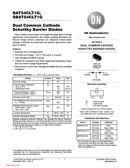
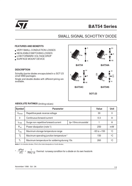
BAT54CLT1G,SBAT54CLT1GDual Common Cathode Schottky Barrier DiodesThese Schottky barrier diodes are designed for high speed switching applications, circuit protection, and voltage clamping. Extremely low forward voltage reduces conduction loss. Miniature surface mount package is excellent for hand−held and portable applications where space is limited.Features∙Extremely Fast Switching Speed∙Low Forward V oltage − 0.35 V (Typ) @ I F = 10 mAdc∙AEC Qualified and PPAP Capable∙S Prefix for Automotive and Other Applications Requiring Unique Site and Control Change Requirements∙These Devices are Pb−Free, Halogen Free/BFR Free and are RoHS Compliant*MAXIMUM RATINGS(T J = 125︒C unless otherwise noted)Rating Symbol Value Unit Reverse Voltage V R30VForward Power Dissipation @ T A = 25︒CDerate above 25︒C P F2251.8mWmW/︒CThermal Resistance (Note 1) Junction-to-Ambient (Note 2)R q JA508311︒C/WForward Current (DC)I F200 Max mANon−Repetitive Peak Forward Current t p < 10 msec I FSM600mARepetitive Peak Forward Current Pulse Wave = 1 sec,Duty Cycle = 66%IFRM300mAJunction Temperature T J−55 to +125︒C Storage Temperature Range T stg−55 to +150︒C Stresses exceeding Maximum Ratings may damage the device. Maximum Ratings are stress ratings only. Functional operation above the Recommended Operating Conditions is not implied. Extended exposure to stresses above the Recommended Operating Conditions may affect device reliability.1.FR−4 @ Minimum Pad.2.FR−4 @ 1.0 x 1.0 inch Pad.*For additional information on our Pb−Free strategy and soldering details, please download the ON Semiconductor Soldering and Mounting Techniques Reference Manual, SOLDERRM/D.30 VOLTDUAL COMMON CATHODE SCHOTTKY BARRIER DIODESCATHODE12MARKING DIAGRAM†For information on tape and reel specifications, including part orientation and tape sizes, please refer to our T ape and Reel Packaging Specifications Brochure, BRD8011/D.SOT−23CASE 318STYLE 95C= Device CodeM= Date CodeG= Pb−Free Package15C M GG*Date Code orientation and/or position mayvary depending upon manufacturing location.Device Package Shipping†ORDERING INFORMATIONBAT54CLT1G SOT−23(Pb−Free)3,000 /Tape & ReelBAT54CLT3G SOT−23(Pb−Free)10,000 /Tape & Reel (*Note: Microdot may be in either location) SBAT54CLT1G SOT−23(Pb−Free)3,000 /Tape & ReelELECTRICAL CHARACTERISTICS (T A = 25 C unless otherwise noted) (EACH DIODE)Characteristic Symbol Min Typ Max UnitReverse Breakdown Voltage (I R = 10 m A)V(BR)R30−−VTotal Capacitance(V R = 1.0 V, f = 1.0 MHz)C T−7.610pFReverse Leakage (V R = 25 V)I R−0.5 2.0m AForward Voltage (I F = 0.1 mAdc)V F−0.220.24VForward Voltage(I F = 30 mAdc)V F−0.410.5VForward Voltage(I F = 100 mAdc)V F−0.520.8VReverse Recovery Time(IF = I R = 10 mAdc, I R(REC) = 1.0 mAdc, Figure 1)trr−− 5.0nsForward Voltage(I F = 1.0 mAdc)V F−0.290.32VForward Voltage(I F = 10 mAdc)V F−0.350.40VNotes: 1. A 2.0 k W variable resistor adjusted for a Forward Current (I F) of 10 mA.2. Input pulse is adjusted so I R(peak) is equal to 10 mA.3. t p » t rrV Rt r10%90%IIOUTPUT PULSE(I F = I R = 10 mA; measuredat i R(REC) = 1 mA)INPUT SIGNALFigure 1. Recovery Time Equivalent Test CircuitC T , T O T A L C A P A C I T A N C E (p F )100V F , FORWARD VOLTAGE (VOLTS)101.00.110V R , REVERSE VOLTAGE (VOLTS)1.00.10.010.001140V R , REVERSE VOLTAGE (VOLTS)124205101530Figure 2. Forward VoltageFigure 3. Leakage CurrentFigure 4. Total Capacitance100100025206810I R , R E V E R S E C U R R E N T (m A )I F , F O R W A R D C U R R E N T (m A )PACKAGE DIMENSIONSSOT −23 (TO −236)CASE 318−08ISSUE APSTYLE 9:PIN 1.ANODE2.ANODE3.CATHODE*For additional information on our Pb −Free strategy and solderingdetails, please download the ON Semiconductor Soldering and Mounting Techniques Reference Manual, SOLDERRM/D.SOLDERING FOOTPRINT*NOTES:1.DIMENSIONING AND TOLERANCING PER ANSI Y14.5M, 1982.2.CONTROLLING DIMENSION: INCH.3.MAXIMUM LEAD THICKNESS INCLUDES LEAD FINISHTHICKNESS. MINIMUM LEAD THICKNESS IS THE MINIMUM THICKNESS OF BASE MATERIAL.4.DIMENSIONS D AND E DO NOT INCLUDE MOLD FLASH,PROTRUSIONS, OR GATE BURRS.VIEW CDIM A MIN NOM MAX MINMILLIMETERS0.89 1.00 1.110.035INCHES A10.010.060.100.001b 0.370.440.500.015c 0.090.130.180.003D 2.80 2.90 3.040.110E 1.20 1.30 1.400.047e 1.78 1.90 2.040.070L 0.100.200.300.0040.0400.0440.0020.0040.0180.0200.0050.0070.1140.1200.0510.0550.0750.0810.0080.012NOM MAX L1 2.10 2.40 2.640.0830.0940.104H E 0.350.540.690.0140.0210.0290−−−100−−−10q︒︒︒︒ON Semiconductor and are registered trademarks of Semiconductor Components Industries, LLC (SCILLC). SCILLC reserves the right to make changes without further notice to any products herein. SCILLC makes no warranty, representation or guarantee regarding the suitability of its products for any particular purpose, nor does SCILLC assume any liability arising out of the application or use of any product or circuit, and specifically disclaims any and all liability, including without limitation special, consequential or incidental damages.“Typical” parameters which may be provided in SCILLC data sheets and/or specifications can and do vary in different applications and actual performance may vary over time. All operating parameters, including “Typicals” must be validated for each customer application by customer’s technical experts. SCILLC does not convey any license under its patent rights nor the rights of others. SCILLC products are not designed, intended, or authorized for use as components in systems intended for surgical implant into the body, or other applications intended to support or sustain life, or for any other application in which the failure of the SCILLC product could create a situation where personal injury or death may occur. Should Buyer purchase or use SCILLC products for any such unintended or unauthorized application, Buyer shall indemnify and hold SCILLC and its officers, employees, subsidiaries, affiliates,and distributors harmless against all claims, costs, damages, and expenses, and reasonable attorney fees arising out of, directly or indirectly, any claim of personal injury or death associated with such unintended or unauthorized use, even if such claim alleges that SCILLC was negligent regarding the design or manufacture of the part. SCILLC is an Equal Opportunity/Affirmative Action Employer. This literature is subject to all applicable copyright laws and is not for resale in any manner.PUBLICATION ORDERING INFORMATION分销商库存信息:ONSEMIBAT54CLT1G BAT54CLT3G。
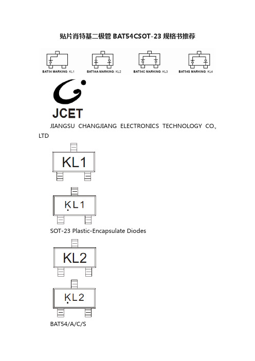
贴片肖特基二极管BAT54CSOT-23规格书推荐
Peak Repetitive Reverse Voltage Working Peak Reverse Voltage DC Blocking Voltage V RRM V RWM V R 30
贴片肖特基二极管 bat54c sot-23规格书推荐 jiangsu changjiang electronics technology co., ltd sot-23 plastic-encapsulate diodes bat54/a/c/s schottky barrier diode features z extremely fast switching speed maximum ratings ( t a =25℃ unless otherwise noted ) parameter symbol value unit peak repetitive reverse voltage working peak reverse voltage dc blocking voltage v rrm v rwm v r 30 v forward continuous current i fm 200 ma non-repetitive peak forward surge current @ t =8.3ms i fsm 600 ma repetitive peak forward current @ t≤1s,δ≤0.5 i frm 300 ma power dissipation p d 200 mw thermal resistance from junction to ambient rΘja 500℃/w junction temperature t j 125℃ storage temperature t stg -55~+150 ℃ electrical characteristics(t a =25℃ unless otherwise specified) parameter symbol min typ max unit test conditions reverse voltage v (br) 30 v i r =100μa forward voltage v f 0.24 v i f1=0.1ma 0.32 v i f2=1ma 0.40 v i f3=10ma 0.50 v i f4=30ma 1 v i f5=100ma reverse current i r 2 μa v r =25v diode capacitance c d 1
BAT54S BAT54肖特基二极管参数
℃
TJ
Operating Junction Temperature工作结温
-55 to +150
℃
电气特性:
符号
Parameter参数
Conditions测试条件
最小
最大
单位
VR
Breakdown Voltage击穿电压
IR30-Fra bibliotekVVF
Forward Voltage正向电压
IF = 0.1mA
IF = IR = 10mA, IRR = 1.0mA,
RL = 100Ω
-
5.0
nS
BAT54封装外型及引脚图
BAT54
BAT54A
BAT54C
BAT54S
BAT54FILM
BAT54AFILM
BAT54CFILM
BAT54SFILM
BAT54S BAT54肖特基二极管参数
来源:|时间:2010年05月02日
三端贴片肖特基二极管BAT54/BAT54A/BAT54C/BAT54S
特点:
极小传导损耗
开关损耗可以忽略不计
低正向压降
表面贴装器件
肖特基势垒二极管封装采用SOT-23
绝对最大额定值:
Symbol符号
Parameter参数
Value数值
Unit单位
VRRM
Maximum Repetitive Reverse Voltage最大重复反向电压
30
V
IF(AV)
Average Rectified Forward Current平均正向电流整流
200
mA
IFSM
肖特基二极管参数表
肖特基二极管参数表摘要:I.肖特基二极管简介A.肖特基二极管的定义B.肖特基二极管的作用II.肖特基二极管参数表A.肖特基二极管的分类B.肖特基二极管的主要参数1.最大重复峰值反向电压2.最大直流阻断电压3.最大正向平均整流电流4.最大瞬时正向电压5.最大直流反向电流C.肖特基二极管参数的重要性III.肖特基二极管参数的选择与应用A.参数选择的原则B.肖特基二极管的应用领域1.电源电路2.通信设备3.电子仪器4.其他领域IV.肖特基二极管的性能与使用寿命A.肖特基二极管的性能优势B.肖特基二极管的使用寿命C.提高肖特基二极管性能和使用寿命的方法正文:肖特基二极管是一种半导体器件,具有单向导通的特性,主要应用于电路中的整流、稳压、保护等场合。
它的参数表是选择和应用肖特基二极管的关键依据。
肖特基二极管参数表主要包括以下几个方面:1.最大重复峰值反向电压:指肖特基二极管能够承受的最大反向电压,决定了二极管在电路中工作的稳定性和可靠性。
2.最大直流阻断电压:肖特基二极管在正向导通状态下,能够承受的最大直流电压。
3.最大正向平均整流电流:肖特基二极管在正向导通状态下,能够承受的最大平均电流。
4.最大瞬时正向电压:指肖特基二极管在正向导通状态下,瞬时承受的最大正向电压。
5.最大直流反向电流:指肖特基二极管在反向截止状态下,能够承受的最大直流反向电流。
这些参数对于选择合适的肖特基二极管至关重要,关系到电路的正常工作和设备的安全。
在选择肖特基二极管参数时,需要根据具体应用场景和电路需求来进行权衡。
例如,对于电源电路,需要关注肖特基二极管的最大重复峰值反向电压和最大直流阻断电压;对于通信设备,需要关注其最大正向平均整流电流和最大瞬时正向电压;对于电子仪器,需要关注最大直流反向电流等参数。
肖特基二极管广泛应用于电源电路、通信设备、电子仪器等领域。
例如,在电源电路中,肖特基二极管可以实现整流、稳压等功能,保证电路的稳定运行;在通信设备中,肖特基二极管可以用于信号放大、开关等电路,提高通信质量和设备性能;在电子仪器中,肖特基二极管可以作为保护元件,防止电路因过电压、过电流等异常情况而受损。
SiC系列产品选型指南肖特基二极管和MOSFET说明书
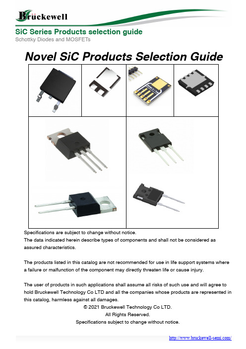
Schottky Diodes and MOSFETsNovel SiC Products Selection GuideSpecifications are subject to change without notice.The data indicated herein describe types of components and shall not be considered as assured characteristics.The products listed in this catalog are not recommended for use in life support systems where a failure or malfunction of the component may directly threaten life or cause injury.The user of products in such applications shall assume all risks of such use and will agree to hold Bruckewell Technology Co LTD and all the companies whose products are represented in this catalog, harmless against all damages.© 2021 Bruckewell Technology Co LTD.All Rights Reserved.Specifications subject to change without notice.Schottky Diodes and MOSFETsIn the recent decades, the Silicon carbide (SiC), turned out to be an excellent semiconductor material. Composed of carbon and silicon, and used in power applications in which it showed excellent performance,far superior to those of silicon.Significant progress has been made in the field of the semiconductor industry, in which the technologies forthe processing of silicon carbide have become increasingly more sophisticated, and have produced semiconductor devices with excellent performance.In the facts those devices during the applications have shown a remarkable capacity to reduce losses and ahigh switching speed in comparison to that offered by silicon. The use of silicon carbide (SiC) as a semiconductor begins to expand into multiple applications and always proves to be more and more the candidate to replace silicon in the most important applications such as automotive and E-Bike motor control.For these reasons, Bruckewell Semi decided to launch the production of the SiC Products, including the SiC Schottky Diode and SiC MOSFET, support the 650V to 1200V, and give the opportunity to its customers totake advantage of the benefits that the products offer in the SiC high-voltage power applications.Present our SiC products line as belowSMD PackageAmp DFN3X3 DFN5X6 TO-277 DFN 8X8 TO-252(DPak) TO-263(D2Pak)4 CBR04P65D6 CBR06P65HL CBR06P65D8 CBR08P65HL CBR08P65D10 CBR10P65HM CBR10P65SCBR10120SCBR10P65HLCBR10P65DCBR10120D20 CBR20120S30 CBR30120H CBR30120S40DFN 3X3 is unique package and CBR10P65HM is first smallest SiC SBD Diode in the industry.TO-277 has same foot print with TO-252 (DPak), and has better thermal performance.Through Hole PackageAmp TO-220AC TO-220AB TO-247 TO-247 (Dual Die)4 CBR04P656 CBR06P658 CBR08P6510 CBR10P65CBR10120 CBR10120PCBR10120W20 CBR20P65CBR20120CBR20P65PCCBR20120PCBR20P65WCBR20120WCBR20P65WCCBR20120WC30 CBR30120W40 CBR40P65WC CBR40120WCSchottky Diodes and MOSFETsPart NomenclatureExample: CBR20P65PC CBR SiC Barrier RectifierCMS SiC MOSFET20 IF, Forward current, as 20AP65 Breakdown Voltage, as P65=650V, 120=1200VPC Package CodeBlank: TO-220AC-2LP: TO-220ABPC: TO-220AB, Dual Die D: TO-252-2L, DPAKW: TO-247-2LWC: TO-247-3L, Dual Die WU: TO-247-3L, Single Die S: TO-277A: SMA, B: SMB, C: SMC B: TO-263, D2PAKH: DFN5x6HM: DFN3x3HL: DFN8x8When the diodes are used simultaneously:ΔTj(diode1) = P(diode1) x Rth(j-c) (per diode) + P(diode2) x Rth(c)To evaluate the conduction losses use the following equation:P = 1.35 x IF(AV) + 0.144 x IF2(RMS)Schottky Diodes and MOSFETsComparison with industry supplier-TO-220AC/ABAmpBruckewellST-MicroInfineonTO-220ACTO-220ABTO-220ACTO-220ABTO-220AC TO-220AB2 IDH02G65C5IDH02G120C53 IDH03SG60C IDH03G65C5 4CBR04P65IDH04SG60C IDH04G65C55 IDH05SG60C IDH05G65C5 IDH05G120C56 CBR06P65 STPSC6TH13TI IDH06SG60C IDH06G65C58 CBR08P65STPSC8TH13TI STPSC8H065CIDH08SG60C IDH08G65C5 IDH08G120C5 9IDH09SG60C IDH09G65C510CBR10P65 CBR10120CBR10120PSTPSC10H065D STPSC10H12D STPSC10TH13TIIDH10SG60CIDH10G65C5 IDH10G120C512 STPSC12065 STPSC1206 STPSC12H065CIDH12SG60C IDH12G65C515 STPSC15H1216STPSC16H065C IDH16G65C5IDH16G120C520CBR20P65 CBR20120CBR20P65PC CBR20120PSTPSC20065D STPSC20H12DSTPSC20H065CIDH20G65C5 IDH20G120C5Note:The suffix C5 in the Infineon Parts means the CoolSiC™ 5G, others are CoolSiC™ 3GSchottky Diodes and MOSFETsComparison with Japan suppliers-TO-220AC/ABAmpBruckewell Rohm Toshiba TO-220AC TO-220AB TO-220AC ITO-220AC TO-220AC ITO-220AC4 CBR04P65 SCS304AP TRS4E65F TRS4A65F5 SCS205KG6 CBR06P65 SCS306APSCS206AGSCS206AM TRS6E65F TRS6A65F8 CBR08P65 SCS308APSCS208AGSCS208AM TRS8E65F TRS8A65F10 CBR10P65CBR10120 CBR10120PSCS310APSCS210AGSCS210KGSCS210AM TRS10E65F TRS10A65F12 SCS212AG SCS212AM15 SCS215AGSCS215KGSCS215AM20 CBR20P65CBR20120CBR20P65PCCBR20120PSCS220AGSCS220KGSCS220AMNote:The suffix of Rohm Parts means the breakdown voltage, A means 650V, K means 1200VSchottky Diodes and MOSFETsComparison with industry supplier-TO-247 Single/ Dual DieAmpBruckewellST-MicroInfineonTO-247 TO-247 DualTO-247TO-247 DualTO-247TO-247 Dual 10 CBR10120WIDW10G65C5 IDW10G120C5B 20 CBR20P65W CBR20120W CBR20P65WC CBR20120WC STPSC20065WSTPSC20H065CWIDW20G65C5IDW20G65C5B IDW20G120C5B12 IDW12G65C515IDW15G120C5B16 IDW16G65C524IDW24G65C5B 30 CBR30120WIDW30G65C5IDW30G120C5B 32IDW32G65C5B 40CBR40120WCSTPSC40065CWIDW40G65C5IDW40G65C5B IDW40G120C5BComparison with Japan suppliers-TO-247 Single/ Dual DieAmpBruckewellRohmFuji electricTO-247 TO-247 DualTO-247TO-247 Dual TO-247 TO-247 Dual10 CBR10120WSCS210KE2FDCY10S6515SCS215AE20 CBR20P65W CBR20120W CBR20P65WC CBR20120WCSCS220AESCS220AE2 SCS220KE2FDCY18S120 FDCY20C6525 FDCY25S6530 CBR30120WSCS230AE2 SCS230KE240 CBR40120WCSCS240AE2 SCS240KE2FDCY36C120 50FDCY50C65Schottky Diodes and MOSFETsProduct IO(A)VB min (V)VF typ(V)IR Max (uA)PackageNumber of Diodes CBR04P65 4 650 1.5 10 TO-220AC 1 CBR04P65D 4 650 1.5 10 DPAK (TO-252) 1 CBR06P65 6 650 1.5 10 TO-220AC 1 CBR06P65D 6 650 1.5 10 DPAK (TO-252) 1 CBR 06P65HL 6 650 1.5 10 DFN 8X8 1 CBR08P65 8 650 1.5 10 TO-220AC 1 CBR08P65D 8 650 1.5 10 DPAK (TO-252) 1 CBR08P65HL 8 650 1.5 10 DFN 8X8 1 CBR10P65 10 650 1.5 10 TO-220AC 1 CBR10P65D 10 650 1.5 10 DPAK (TO-252) 1 CBR10P65S 10 650 1.5 10 TO-277 1 CBR10P65HM 10 650 1.5 10 DFN3.3 1 CBR10P65HL 10 650 1.5 10 DFN8X8 1 CBR20P65PC 20 650 1.5 10 TO-220AB 2 CBR20P65 20 650 1.5 10 TO-220AC 1 CBR20P65W 20 650 1.5 10 TO-247 1 CBR20P65WC 20 650 1.5 10 TO-247 2 CBR40P65WC 40 650 1.5 10 TO-247 2 CBR10120 10 1200 1.5 10 TO-220AC 1 CBR10120P 10 1200 1.5 10 TO-220AB 1 CBR10120D 10 1200 1.5 10 DPAK (TO-252) 1 CBR10120S 10 1200 1.5 10 TO-277 1 CBR10120W 10 1200 1.5 10 TO-247 1 CBR20120WC 20 1200 1.5 10 TO-247 2 CBR20120W 20 1200 1.5 10 TO-247 1 CBR20120 20 1200 1.5 10 TO-220AC 1 CBR20120P 20 1200 1.5 10 TO-220AB 1 CBR20120PC 20 1200 1.5 10 TO-220AB 2 CBR20120S 20 1200 1.5 10 TO-277 1 CBR30120W 30 1200 1.5 10 TO-247 1 CBR30120S 30 1200 1.5 10 TO-277 1 CBR30120H 30 1200 1.5 10 DFN 5X6 1 CBR40120WC 4012001.510 TO-2472Schottky Diodes and MOSFETsDisclaimerALL PRODUCT, PRODUCT SPECIFICATIONS AND DATA ARE SUBJECT TO CHANGE WITHOUT NOTICE TO IMPROVE RELIABILITY, FUNCTION OR DESIGN OR OTHERWISE. Bruckewell Technology Inc., its affiliates, agents, and employees, and all persons acting on its or their behalf (collectively, “Bruckewell”), disclaim any and all liability for any errors, inaccuracies or incompleteness contained in any datasheet or in any other disclosure relating to any product. Bruckewell makes no warranty, representation or guarantee regarding the suitability of the products for any particular purpose or the continuing production of any product. To the maximum extent permitted by applicable law, Bruckewell disclaims(i) Any and all liability arising out of the application or use of any product.(ii) Any and all liability, including without limitation special, consequential or incidental damages. (iii) Any and all implied warranties, including warranties of fitness for particular purpose, non-infringement and merchantability.Statements regarding the suitability of products for certain types of applications are based on Bruckewell’s knowledge of typical requirements that are often placed on Bruckewell products in generic applications.Such statements are not binding statements about the suitability of products for a particular application. It is the customer’s responsibility to validate that a particular product with the properties described in the product specification is suitable for use in a particular application. Parameters provided in datasheets and/or specifications may vary in different applications and performance may vary over time.Product specifications do not expand or otherwise modify Bruckewell’s terms and conditions of purchase, including but not limited to the warranty expressed therein.。
BAT54 Series中文资料
A1 K2
BAT54A
A2 A1 K2
K
K1 A2
K1
BAT54C SOT-23
BAT54S
ABSOLUTE RATINGS (limiting values) Symbol VRRM IF IFSM Ptot Tstg Tj TL Parameter Repetitive peak reverse voltage Continuous forward current Surge non repetitive forward current Power dissipation (note 1) Maximum storage temperature range Maximum operating junction temperature * Maximum temperature for soldering durong 10s tp=10ms sinusoidal Value 30 0.3 1 250 - 65 to +150 150 260 Unit V A A mW °C °C °C
Note 1: for double diodes, Ptot is the total dissipation of both diodes
* :
1 dPtot < thermal runaway condition for a diode on its own heatsink Rth(j−a) dTj
2.35 0.92
1.9 0.075
2 0.079 1 0.040 mm inch
0.9 0.035
0.9 0.035
Information furnished is believed to be accurate and reliable. However, STMicroelectronics assumes no responsibility for the consequences of use of such information nor for any infringementof patents or other rights of third parties which may result from its use. No license is granted by implication or otherwise under any patent or patent rights of STMicroelectronics. Specifications mentioned in this publication are subject to change without notice. This publication supersedes and replaces all information previously supplied. STMicroelectronics products are not authorized for use as critical components in life support devices or systems without express written approval of STMicroelectronics.
DIODES SOT523肖特基二极管BAT54T选型手册

May 2018
© Diodes Incorporated
CT, TOTAL CAPACITANCE (pF) PD, POWER DISSIPATION (mW)
12 10
8
6 4
2
0
0
5
10
15
20
25
30
VR, DC REVERSE VOLTAGE (V)
Fig. 3 Total Capacitance vs. Reverse Voltage
Solderable per MIL-STD-202, Method 208 Lead-Free Plating Polarity: See Diagrams Below Weight: 0.002 grams (Approximate)
Top View
BAT54T
BAT54AT
BAT54CT
BAT54ST
Ordering Information (Note 4)
Notes:
Part Number
Case
Packaging
BAT54T-7-F
SOT523
3,000/Tape & Reel
BAT54AT-7-F
SOT523
3,000/Tape & Reel
BAT54CT-7-F
SOT523
1
100
IF, INSTANTANEOUS FORWARD CURRENT (A)
10 0.1
1 0.01
0.1
0.001 0.01
0.0001 0
0.2
0.4
0.6
0.8
1.0
VF, INSTANTANEOUS FORWARD VOLTAGE (V)
TBAT54,LM(T肖特基二极管东芝最新资料
3
2016-05-12 Rev.1.0
TBAT54,TBAT54A,TBAT54C,TBAT54S
Package Dimensions
Unit: mm
Weight: 0.0125 g (typ.)
Package Name(s) TOSHIBA: 2-3AB1A Nickname: SOT23
©2016 Toshiba Corporation
TBAT54,TBAT54A,TBAT54C,TBAT54S
Schottky Barrier Diode Silicon Epitaxial
TBAT54,TBAT54A,TBAT54C,TBAT54S
1. Applications
• Ultra-High-Speed Switching
2. Packaging
5. Absolute Maximum Ratings (Note) (Unless otherwise specified, Ta = 25 )
Characteristics Peak reverse voltage Reverse voltage Average rectified current Peak forward current Non-repetitive peak forward surge current Power dissipation Junction temperature Storage temperature Symbol VRM VR IO IFM IFSM PD Tj Tstg (Note 3) (Note 3) (Note 1), (Note 3) (Note 2), (Note 3) Note Rating 35 30 200 300 1 320 150 -55 to 150 A mW mA Unit V
- 1、下载文档前请自行甄别文档内容的完整性,平台不提供额外的编辑、内容补充、找答案等附加服务。
- 2、"仅部分预览"的文档,不可在线预览部分如存在完整性等问题,可反馈申请退款(可完整预览的文档不适用该条件!)。
- 3、如文档侵犯您的权益,请联系客服反馈,我们会尽快为您处理(人工客服工作时间:9:00-18:30)。
Symbol
Min
Typ Max Unit
V (BR)
30
V
VF1
0.24
V
VF2
0.32
V
VF3
0.40
V
VF4
0.50
V
VF5
1
V
IR
2
μA
CD
10
pF
Reverse recovery time
trr
5
ns
Unit
V
mA mW ℃/W ℃
Symbol VRRM VRWM
VR IFM PD RθJA Tj TSTG
Limit
30
200 200 500 125 -55~+150
Electrical Characteristics @Ta=25℃
Parameter Reverse breakdown voltage
Forward voltage
【领先的片式无源器件整合供应商—南京南山半导体有限公司】
JIANGSU CHANGJIANG ELECTRONICS TECHNOLOGY CO., LTD
SOT-23 Plastic-Hale Waihona Puke ncapsulate Diodes
BA T54/A/C/S SCHOTTKY BARRIER DIODE
BAT54/A/C/S
REVERSE CURRENT IR (uA)
FORWARD CURRENT IF (mA)
Forward Characteristics
1000
100
oC
T
=100
a
10
oC
=2 5
T a
1
0.1
Reverse Characteristics
100
网址:
□技术 □采购 □贸易商 邮箱:
元器件明细资料
元器件名称 型号及封装
单机用量 申请数量 备注
预计生产情况
预计小批量生产时间:
规模生产时间:
样品申请时间:
样品申请流程
1、请详细、全面、真实填写上列各项。表格不够填写,可自行复制。 2、请以附件的形式将该文档通过 E-mail 发送,并请客户将此单打印盖章后 邮件至:Service@nsc。 。 3、公司将根据客户所填信息并综合相关情况,及时确定该样品申请是否执行及如何执行。 4、收到样品申请单并经审核通过后,南京公司有现货24小时内发出,如需订货,交期3-4周,非常规品顺延1-2 周。 5、样品免费,运费到付(一般选择顺丰快递);样品数量规定:单个型号5~20pcs, 或按单机数量2~5套。 6、特别说明:由于体制约束等不确定因素,我们并不保证样品数量和型号完全符合要求,也不承诺一定按期 交出。
FEATURES z Extremely Fast Switching Speed
SOT-23
BAT54 MARKING: KL1
BAT54A MARKING: KL2
BAT54C MARKING: KL3
BAT54S MARKING: KL4
Maximum Ratings @Ta=25℃
Parameter Peak Repetitive Peak Reverse Voltage Working Peak Reverse Voltage DC Blocking Voltage Forward Continuous Current Power Dissipation Thermal Resistance Junction to Ambient Junction temperature Storage Temperature
℃
Conditions IR=100μA IF=0.1mA IF=1mA IF=10mA IF=30mA IF=100mA VR=25V
VR=1V,f=1MHz IF=IR=10mA
Irr=0.1XIR,RL=100Ω
B,Jul,2012
【领先的片式无源器件整合供应商—南京南山半导体有限公司】
Typical Characteristics
回访记录
□已联系确认 日期:
□已建议执行 日期:
□未发送但已下单 日期:
□已发送样品 日期:
□客户已签收 日期:
第1页共1页
16
12
8
4
0
0
5
10
15
20
25
30
REVERSE VOLTAGE VR (V)
POWER DISSIPATION PD (mW)
Power Derating Curve
300
250
200
150
100
50
0
0
25
50
75
100
125
150
AMBIENT TEMPERATURE Ta (℃)
CAPACITANCE BETWEEN TERMINALS CT (pF)
B,Jul,2012
【领先的片式无源器件整合供应商—南京南山半导体有限公司】
联系资料
电话:
南京南山半导体有限公司-样品申请单
技术支持:
传真:
电邮:Service@
客户基本资料
公司名称
联系方式
电话:
收货地址
主要产品
联络人
姓名:
电话:
传真:
职务: 手机:
Ta=100 oC 10
1 Ta=25 oC
0.1
0.01 0
200
400
600
800
1000
FORWARD VOLTAGE VF (mV)
0.01 0
5
10
15
20
25
30
REVERSE VOLTAGE VR (V)
Capacitance Characteristics
20 Ta=25℃ f=1MHz