Xilinx Platform Studio的使用流程
Xilinx使用步骤.doc

Xilinx使用步骤:第一步:打开Xilinx→打开File→点击New Project然后输入工程名qq,点击Next点击Next点击Next点击New Source→点击VHDL Module→在File name处输入文件名Cui→点击下一步端口的名字自己随便写,这是两个输入端a,b。
一个输出端c。
用来实现与门的功能,继续点击Next点击Finish点击Yes然后继续点击下一步,下一步,直到点击Finish,将出现此对话框然后大概到39行左右(begin 与end Behavioral之间)就可以输入VHDL 代码。
例如:输入c<=a and b;//实现与门的功能。
然后点击保存(这个很重要)然后点击运行如果程序正确,将运行成功,如下然后可以查看(老师说这种图要保存):在这个图上继续点击(双击):(这个图要保存)第二步:仿真测试在Sources For处修改Synthesis/Implementation为Behavioral Simulation,然后再cui- Behavioral右击NewSource,结果如下:添加Test Bench WaveForm,及File Name,然后下一步然后下一步,下一步,下一步……直到Finish屏幕上b处的波形是可以点出来的,b处必须有波动,不可以是直线,然后必须保存,如下:然后点击Processes,右击Simulate Behavioral Model ,点击运行将出现以下结果点击Wave default,就可以看到结果(这个要保存),如下(F5、F6调大小):大家不懂得问哦!!!这个工程要保存下来,用来答辩!!!。
XilinxPlatformStudio教程

XPS - Processor Selection
• Choice as to which processor to use in our SoC.
• PowerPC:
• PPC405 Hard Core. • Physical CPU embedded
within FPGA fabric.
• MicroBlaze:
Write SW to “make things work”.
• Iterate if needed.
• The FPGA has a malleable fabric…
• So both SW and HW are flexible and can be changed…
• At “compile-time”. • At “run-time” (dynamic reconfiguration).
• A file that lists all components and how they are configured and connected.
• This file can be translated directly to VHDL or Verilog, and synthesized to the FPGA.
• This is done by selecting “Device Configuration”.
• “Update Bitstream” - combines HW/SW (.bit + .elf). • “Download Bitstream” - downloads the configuration to the
• STDIN = UART. • STDOUT = UART.
赛灵思PLATFORM STUDIO SUITE7.1简化嵌入式系统

赛灵思PLATFORM STUDIO SUITE7.1简化嵌入式系统
佚名
【期刊名称】《世界仪表与自动化》
【年(卷),期】2005(009)004
【摘要】赛灵思公司近日宣布推出针对平台FPGA嵌入式处理设计的Platform Studio工具套件7.1i版。
这款新版工具利用新推出Xilinx(Virtex-4 FX器件中突破性的嵌入式功能可简化开发过程。
Xilinx(Virtex-4 FX器件拥有业界唯一的嵌入
式双PowerPC处理器和用于加快处理功能的创新的辅助处理器单元(APU)控制器。
7.1i版集成了FPGA设计中前所未有的多种增强型使用功能和新特性,可进一步简化、概括和加快嵌入式系统的开发。
【总页数】1页(P62)
【正文语种】中文
【中图分类】TP316
【相关文献】
1.赛灵思针对工业自动化简化实时以太网网络开发 [J],
2.赛灵思推出新型MICROBLAZE嵌入式套件可使嵌入式系统设计快速启动 [J],
3.赛灵思新版本平台整合全新图形UI简化嵌入式设计 [J], 无
4.赛灵思新推VIRTEX-5协议包简化PCI Express、千兆以太网和XAUI设计 [J],
5.“北工大—赛灵思软件工程(嵌入式系统方向)联合人才培养模式创新实验区”开园暨“第二届开放源码硬件与嵌入式大赛”开赛 [J], 迎九
因版权原因,仅展示原文概要,查看原文内容请购买。
(完整版)XilinxSDK使用教程

Xilinx SDK使用教程本文参考Xilinx SDK软件内置的教程,打开方法:打开SDK->Help->Cheet Sheets...->Xilinx SDK Tutorials,这里有6篇文档。
本文详细介绍其中的4篇(与Application相关)如何创建一个新的软件应用1.打开SDK,切换到c/c++界面下。
(有两个界面,还有一个是Debug界面,在软件右上角处切换)2.指定一个新的硬件平台项目在SDK开发软件时,需要指定硬件平台。
(如果你打开一个现成的SDK工作空间,这一步可以省略)如果SDK工作空间中没有指定,BSP新建窗口会弹出,询问你硬件平台。
---File > New > Other > Xilinx > Hardware Platform Specification---Next, 显示新的硬件项目对话框。
---设定项目名称,以及由Vivado产生的硬件平台。
---Finish.3.创建一个独立的板级支持包(Board Support Package )---File > New > Board Support Package,打开对话框。
---指定新项目的名字(已初始一个默认的名称)---从CPU下拉列表中,选择目标处理器---从BSP OS下拉列表中,选择操作系统,默认是standalone(没有操作系统)---Finish.弹出BSP设置对话框---配置参数,生成一个BSP---OK4.创建应用项目---File > New > Application Project---指定项目名称---选择OS---选择目标硬件平台---选择目标处理器---选择编程语言---选择一个现有的BSP,或者新建一个---Next---选择一个模板,生成一个可直接运行的软件工程---Finish如何调试一个软件应用1.配置目标连接如果你想用本地设备,你可以跳过这个步骤。
xilinx platform studio 教程
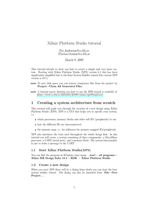
Xilinx Platform Studio tutorialPer.Anderson@cs.lth.seFlavius.Gruian@cs.lth.seMarch9,2009This tutorial intends to show you how to create a simple and very basic sys-tem.Starting with Xilinx Platform Studio(XPS)version6.1this has been significantly simplified due to the Base System Builder wizard(the current XPS version is10.1).note To save disk space you can remove temporaryfiles from the project by Project→Clean All Generated Files.note A tutorial movie showing you how to use the BSB wizard is available at http://www.cs.lth.se/EDA385/HT08/videos/xpsWizard.avi1Creating a system architecture from scratch This tutorial will guide you through the creation of a new design using Xilinx Platform Studio(XPS).XPS is a GUI that helps you to specify your system, i.e.•which processors,memory blocks and other soft IPs(peripherals)to use•how the different IPs are interconnected•the memory map,i.e.for addresses for memory mapped IO/peripheralsXPS also interfaces the tools used throughout the whole designflow.In this tutorial you will create a system consisting of three components,a MicroBlaze processor,a UART(serial port),and a memory block.The system functionality is just to write a message to the UART.1.1Start Xilinx Platform Studio(XPS)You canfind the program in Windows start menu.start→all programs→Xilinx ISE Design Suite10.1→EDK→Xilinx Platform Studio1.2Create a new designWhen you start XPS there will be a dialog from which you can start the base system builder wizard.The dialog can also be launched from File→New Project...1•In thefirst wizard dialog,specify the project location and name(the path cannot contain spaces).XPS will create a lot offiles in the project direc-tory,so create a new empty directory.You will also need to check the Set Project Peripheral Repositories box,and write in the path to the Digilent BSBfiles,if you are using the Digilent boards(C:\XILINX\Nexys_BSP\lib).Click OK.•In the new dialog select“I would like to create a new design”,Click Next.•In the new dialog set the target board as follows:Board Vendor DigilentBoard Name Nexys2-1200BoardBoard Revision CClick Next.•MicroBlaze is the only available processor option,so click Next.•Keep the50MHz clock,but you may remove the debug interface.During the labs it is recommended to increase the size of the local memory to at least16KB.To continue click Next.•At this step you may choose which board components(LEDs,buttons, switches etc.)you want to create interfaces for.Keep whichever LEDs and buttons,and click next.•Keep the RS232(UART)which will be your STDIN and STDOUT(for the C IO functions,i.e.printf()and scanf()).•Make sure you uncheck the Micron RAM and Intel Flash.These are in-terfaces to the off-chip,on-board RAM and Flash memories,which you will not be using.The system will function properly with on-chip memory only.You do not need other extra peripherals for now,next.•Now you are done,click next in the remaining dialogs,Generate and Finish.After this you want to“Start using Platform Studio”.You have created your initial system.All you need to do now is compile and run logic synthesis,as will be explained later.Now is a good time to explore XPS a bit.Lets start by looking into the hardware architecture generated for you.It can be visualised by selecting Project→Generate and View Block Diagram.A block diagram will appear in the frame to the right1. Do not worry if you do not get all the abbreviations.Here is a partial list: LMB Local Memory Bus CPU↔memory bus(point to point bus) PLB Processor Local Bus CPU↔peripheral bus(shared bus)GPIO General Purpose IO glue logic for the buttons/leds on the board RS232serial port used for text input/output of your application An extended view which also contains more information about the components is created by selecting Project→Generate and View Design Report.1If the picture will appear only as a broken image in a web browser,you should do the following.Open Edit→Preferences→Block Diagram and select the PNG radio button instead of SVG in the dialog that pops up.You should obtain a proper picture now.2There are three main frames in the XPS window.Lets start with the left frame.It contains three tabs Project,Applications,and IP Catalog.In the Project tab youfind general systemfiles as well as logfiles,in the Application tab youfind the software parts of your system,andfinally in the IP Catalog you find a tree containing all the IP components you can use to build your system.Select the Application tab.There are two projects,one for memory test and one for peripheral test.The projects which are not active(downloaded)have a red cross in their icon.Right click on a project and select Mark to Initialize BRAMs to activate it.By right clicking you can also compile(build)individual software projects.There can only be one main function for every processor,so do not activate several projects that contain a main function.The frame to the right in the XPS window is used for viewing and editing documents.This is where you opened the block diagram earlier.Select the System Assembly tab(the tabs are in the bottom of the frame).This view contains a list/tree of your system components and their connections.There are three busses.The two blue are LMBs connecting the processor and the memory controller,one is used for instruction fetch(ilmb)and the other is used for data read/write(dlmb).The red lines are not buses,but illustrate the connection between the memory controller and the memory block(s).Finally the gold line is a PLB connecting the processor and the peripherals.All peripherals are memory mapped,thus they can be addressed through read/write to memory addresses(see the Addresses tab).To connect/disconnect a component to/from a bus click on the circles.Double click on a component to get a dialog in which you can change its parameters.2Building your systemXPS keeps track of all dependencies in your system and will automatically rebuild the parts which are affected if you change a parameter or edit afile. You can select Device Configuration→Update Bitstream and the tool will build the whole system and prepare the configurationfile for the FPGA. To download and run this onto the FPGA you must use another application, specific for the Digilent boards.All these step are explained below.First,let’s have a look at the software part.In a system,the user pro-grams access the hardware resources via libraries.XPS automatically con-figures and generates the library code for your system.To do this,select( Software→Generate Libraries and BSPs).This step also generates header files containing symbolic names for memory mapped peripherals.Run this step and look at your software projects(the Applications tab in the left frame). Click on the+left of processor:microblaze0in your active project.There you willfind a headerfile(xparameters.h)with symbolic names of all mem-ory mapped e the symbolic names in your C code,so you can change the memory layout later without changing the C code.Headerfiles are also generated(if necessary)under Headers(the same level in the tree as proces-sor:microblaze0).Here you willfind functions specific to your peripherals,for example functions to read/write from/to GPIO.Note,the standard C function printf generates huge libraries,which will notfit in the small on-chip memory. Instead use print,or xil printf functions to output text.xil printf is sim-ilar to printf,but much smaller and lacks some of the formatting,i.e.floating3point support.If you want to discover more about the software settings,have a look at Software→Software Platform Settings....Now compile your programs by selecting Software→Build All User Applications.Let’s move on to the hardware.Hardware synthesis is done in several steps (create the logic circuit(netlist),create the FPGA configuration(bitmap)),but you do not need to worry about this just yet.Simply select Hardware→Gen-erate Bitstream and everything will be generated automatically for you.This might take a long time,in the range of10minutes or even more.Fortunately the hardware is independent of the software,so whenever you change your C files,this step will not rerun.During the hardware synthesis,the tools use a User Constraint File(UCF),which can be found in the left frame in the Project tab.Thisfile binds external ports in your design to physical pins on the FPGA. It is important that the names in the design are the same as in thisfile,so do not rename the external ports.Also if you add or remove external pins thisfile must be edited,i.e.removing a GPIO peripheral.The last step before dowloading the configuration to the FPGA is to merge software binaries and the bit stream from the hardware synthesis,run Device Configuration→Update Bitstream.This places the executable in the on-chip memory,making the configurationfile ready to be downloaded on the FPGA.2.1Run thefinal implementation on the FPGAWhen you run your system it is nice to see some output,i.e.the result of print().The text is forwarded to the serial port(STDOUT being set to the RS232device)and to monitor this we can use the windows hypertermi-nal start→all programs→accessories→communications→hyperter-minal.Give the new connection a new name and chose com1in the Connect using e port settings according to the uart parameters:Bits per second9600Data bits8Parity NoneStop bits1Flow control NoneThis must be the same as the configuration of the RS232peripheral.Feel free to change the speed of the UART,but beware,if you change the peripheral parameters you must run hardware synthesis again.Now you are about to run the system and you need a FPGA board,connect it(both the USB and the RS232cables)and switch the power on.The Digilent boards can be configured with the system you just synthesized using a specific program,found in start→all programs→Xilinx ISE Design Suite10.1→Adept(Digilent)→ExPort.At this point you should have a new window called Digilent ExPort.Do the following:•Check the Auto-Detect USB box•Click on the Initialize Chain button to detect the configurable devices accessible through the JTAG.At this point you should be able to see two devices-one being the FPGA,xc3s1200e,and one being the ROM device4for the boot configuration xcf04s.(If this does not happen,check your USB connection again).We will only configure the FPGA directly,so •Check the ROM box to bypass it•Click Browse and select the download.bit configurationfile from your project directory home,under implementation/•Finally,click the Program Chain button to configure the FPGAThe system should start to run directly.Depending on the application you selected for BRAM Initialization,you may see some LEDs blinking and text messages in the hyperterminal(this assumes you are running the peripheral test application).Press the button labelled BTN0on the FPGA board to restart the program(will give a new printout).XPS keeps track of most dependencies among the sourcefiles,so if you change anything,selecting a download to the FPGA will rebuild all parts that are affected.You can force XPS to rerun a step by choosing Software→Clean Software and Hardware→Clean Hardware.This removes all generated files,thus it also saves disk space.3That was easy,what’s next?You should have by now created and run yourfirst e the remaining time in thefirst lab to explore the XPS program.The following labs will contain much more work and you will not be able tofinish unless you have prepared ahead,i.e.created the system.In the next lab you will need a system consisting of a MicroBlaze,a RS232(xps uartlite)and a timer(xps timer).If you have time you can start to create this system.Read the documentation of the timer. Tofind the documentation,right click on it in the IP Catalog tab in the left XPS frame.4Dual processor and FSL communicationLet’s continue by creating a dual processor system,that will be needed in lab 3.Start by creating a system containing only one MicroBlaze and a RS232 (xps uartlite)using the BSB wizard(or continue working with the system you just created).To add a second processor you need to manually duplicate all components and parameters in the processor/memory subsystem.Look at the block diagram to see how the memory and CPU are connected(CPU↔LMB↔LMB controller↔memory block).Notice that MicroBlaze uses a Harvard ar-chitecture,where data and instructions have separate pathways.On the other hand,the memory blocks are dual ported,meaning that you can connect both the instruction and data bus to the same memory block.To add IP components to your design,select the IP from the IP Catalog tab in the left XPS frame,and double-click on it.The newly added IP should appear in the System Assembly tab,where you can also rename the instance.Now add the following:•one Processor→microblaze,•one Memory Block→bram block,5•two Memory Controllers→lmb bram if ctrl,•two Buses→lmb v10,•two Fast Simplex Link Buses→fsl v20).Connect the components you’ve just added.The processor should also be connected to the common PLB bus.This is done in the System Assembly tab. Make sure that the Bus Interface tab is selected.All busses are shown to the left (vertical lines).Simply click on a circle/box to connect a component instance to a bus.You can only connect ports on an instance,so click on the+to see the component portsfirst.Fast Simplex Link(FSL)is a uni-directional point to point connection which will be used to communicate directly between the processors.To use them, you must add FSL ports to the processors.To do this,double click on the processor,select the Bus Interface tab and change Number of FSL Links to one (meaning one duplex interface,with a master port and a slave port).Connect the processors to the FSL busses.A FSL is directed,so one processor should write(master)and the other should read(slave)on the same FSL.To have communication in both directions you need two FSLs.Your system should be looking something like in Figure1.Figure1:Dual MicroBlaze system viewYou also need to connect the clock and reset signals.Change thefilter from Bus Interface to Ports.First connect the reset signal of the newly added pro-cessor to the mb reset signal.Connect all four buses you added to the nets sys clk s and sys bus reset(click on No Connection and select the appro-priate signal).Your ports should be connected now as depicted in Figure2.6Figure2:Ports Connection7Let’s move on to the memory layout of the newly added processor.Change the filter from Ports to Addresses .The two new LMBs have unknown address space.Set the memory size to 16K for both,which will result in Base Address set to 0x00000000and High Address set to ing more than 16K might make your system too large to fit on the FPGA.Now,that the hardware system is set up properly,let’s continue with the software.You must direct STDIN or STDOUT of the new processor to the common serial port.Select Software →Software Platform Settings .Select the new processor,under OS and Libraries assign STDIN and STDOUT to RS232PORT .Finally you also need a program to run on the second processor.In the left frame,select the Applications tab.You should have two projects.Lets run one on each processor.To select the target processor for a project open its tree structure (click on the +to the left),right click on Processor:...and select the target processor.Make sure both projects are Mark to Initialize BRAMs (if not right click on Project:...).Thats all you need to do.Run hardware synthesis,software compilation,and configure (download to)the FPGA.4.1FSL communicationOnce you have got both CPUs running (messages from both show up on the terminal),it is time to do something useful.Let’s make them talk to each other,through the FSL.Macros for reading and writing from/to the FSL are already available in a header file that should be included in your sources mb interface.h ,file that can be found in under your_project\microblaze_0\include .The commonly used macros are putfsl(data,port)and getfsl(data,port).Both are blocking,data is the data to read/write.For the read/get operation it must be a variable,which then will be updated to contain the value read,port is the FSL port number,starting from 0.Example program (assuming there is a FSL in both directions):MicroBlaze 0:MicroBlaze 1:#include <mb_interface.h>#include <xutil.h>int main(void){int i =0;while(i<10){putfsl(i,0);getfsl(i,0);xil_printf("pong %d\n\r",i);}}#include <mb_interface.h>#include <xutil.h>int main(void){int i;while(1){getfsl(i,0);i++;xil_printf("ping %d\n\r",i);putfsl(i,0);}}8。
MB使用心得

今天在网上的高人(青芷蓝烟)指点,用chipscope调试MB,不过到目前(2006-3-27 17:17pm)还没有搞出来。
青芷蓝烟(30840814) 16:47:50我的意思是,EDK中不要那个chipscope的核和mdm 而是将它的project option 设为submode 将它Export to ProjNav青芷蓝烟(30840814) 16:48:19在那里新建一个cdc 文件,调用chipscope海洋深处~(4704295) 16:55:53export to Projnav 是什么啊,弄到ISE里面?青芷蓝烟(30840814) 16:49:01就是完全和在ISE中使用chipscope 一样青芷蓝烟(30840814) 16:49:17你看你的option 选项海洋深处~(4704295) 16:56:35哦青芷蓝烟(30840814) 16:49:37里面有project options青芷蓝烟(30840814) 16:50:04打开就可以看到可以设置你的project是top mode haishi sub mode海洋深处~(4704295) 16:57:44哦,这里有选项青芷蓝烟(30840814) 16:50:56你把它设为submode青芷蓝烟(30840814) 16:51:07然后生成网表海洋深处~(4704295) 16:58:11嗯,设了海洋深处~(4704295) 16:58:14哦青芷蓝烟(30840814) 16:51:37再在Tools->Export to ProjNav海洋深处~(4704295) 16:59:00哦海洋深处~(4704295) 16:59:19这些是哪里看到的哦,自己领悟的?青芷蓝烟(30840814) 16:53:19这个是某个指南上有的应该就在EDK->doc 里青芷蓝烟(30840814) 16:53:43也许是system tools 指南,也许是XPS 指南,忘了:)海洋深处~(4704295) 17:00:56哦海洋深处~(4704295) 17:01:07我太着急了,没有看海洋深处~(4704295) 17:01:10来不及看海洋深处~(4704295) 17:01:12唉。
ISE中应用MicroBlaze软核
Siga-S16_ISE中使用MicroBlaze软核Rev. 1.00版本记录版本时间作者描述ReleaseLuo FirstRev1.00 2012-6-20一、前言在FPGA实际开发中,有时会用MicroBlaze软核做为主控芯片,再在处理器周围设计一些独立的逻辑电路或包含其它的功能模块。
这样对于MicroBlaze系统开发部分,可以由熟悉单片机及C语言开发的人开发。
对于逻辑部分,就由熟悉Verilog 语言进行项目的开发。
在FPGA的设计项目中嵌入MicroBlaze软核将会起到事半功倍的效果。
下面就在ISE如何使用Microblaze软核,写一个简单的入门教程。
教程以图片为主,辅以简单的文字进行说明。
实验使用的是Siga-S16 Spartan 6的FPGA开发板,开发环境为ISE13.1。
本文档分为以下几个部分:1、ISE创建顶层文件2、ISE创建Microblaze软核3、ISE 创建Verilog文件4、设计/添加Microblaze的应用程序5、创建UCF文件6.编译和下载1. ISE创建顶层文件¾先在ISE中创建一个ISE工程。
选择菜单:File→New Project,在弹出的对话框中输入工程名字。
这里为ISE_Microblaze,在Top-level source type一栏中选择Schematics。
在这里选择Siga-S16开发板上的FPGA型号。
根据自己开发习惯,选择是使用Verilog语言还是VHDL语言。
点击Finish完成。
工程创建完成,现在的工程ISE_MB_TEST里还没有其它文件。
¾向工程中添加顶层文件我们添加原理图文件作为项目的顶层文件,右键点击工程,选择New Source…。
在弹出的对话框中选择Schematics,文件名和工程名一致。
点击Finish完成。
2. ISE创建Microblaze软核右键点击顶层文件ISE_MB_TEST,选择New Source…。
可编程片上系统开发平台
基于设计人员选择的板子,设计人员通过BSB选择并 配置基本的元素,比如:处理器类型、调试接口、缓存配 置、存储器类型和大小、外设等。 对于BSB不支持的目标系统,设计人员可以选择定制 板选项。使用这个选项时,必须指定未来板子的硬件,并 且要给出用户约束文件UCF。 如果选择的是支持的目标板,BSB向导自动的加入 UCF文件。当退出BSB时,BSB所建立的MHS和MSS文 件自动加入到XPS工程中,设计人员能在XPS中进行更进 一步的设计。
软件开发
Library Generator(Libgen)
构建一个软件平台,该软件平台由定制的软件库、驱动程序和OS构成。
GNU Compiler Tools(GCC)
基于库产生器建立的平台,建立软件应用程序。
验证
Xilinx Microprocessor Debugger(XMD)
打开shell用于软件下载和调试,也提供通道用于GNU调试器访问设备。
设计流程及EDK工具 - Xilinx Platform Studio(XPS)
XPS提供下面的特性: (1) 能够添加核,编辑核参数和进行总线和信号连接,产生MHS 文件; (2) 能够产生和修改MSS文件; (3) 支持表5.1内的所有工具; (4) 能够产生和观察系统块图和设计报告; (5) 多用户软件应用支持; (6) 项目管理; (7) 过程和工具流程依赖管理; (8) 输出MHS文件到SDK工具
在主机上建立一个MFS存储器镜像,该镜像并被下载到嵌入式系统存储器。
Platform Specification Utility
自动产生微处理器外设定义MPD数据文件,该文件要求创建EDK兼容的制定外设。
xilinx使用步骤
Xilinx软件使用步骤目录基本操作1. 打开xilinx2. open project3. New project4. 创建新的 .vhd文件5. 建立波形文件6. 综合7. 仿真8. 下载程序到电路板中需要注意的问题1.生成顶层原理图2.建立.ucf文件3. implement时出错的原因4.仿真时的问题基本操作1. 打开xilinx图1 打开xilinx界面2. open project图2 open project图3 查找要打开的.ise文件单击打开后,出现在左侧box中。
图4 open project3. New project顶层文件类型,原理图类型选Schematic,否则选择HDL;单击下一步,通过右侧value各项目,配置器件类型,即FPGA 型号。
注意:此处配置错误的话,综合时会出现放不下或者些不进去的错误。
配置完成后,单击下一步,出现创建源文件对话框如下图所示。
不需做设置更改,直接点击下一步,出现添加现有源对话框如下图所示。
不需做任何设置,直接单击下一步,出现New project information对话框,如下图所示。
确认信息无误后,单击完成,创建的新的project即出现在主页面左侧Sources in project中,如下图所示。
4. 创建新的 .vhd文件右击主页面左侧Sources in project中xc2s200-5pq208,在右键菜单中选择New source,如下图所示;出现New source对话框;左侧选择VHDL Module,右侧输入文件名,如下图所示,单击下一步;出现define vhdl source对话框,输入端口名,输入输出类型和MSB,LSB, 如下图所示,然后单击下一步,出现信息对话框,如下图所示,确认无误后,单击完成。
然后主页面如下图所示:5. 建立波形文件在主页面,编程之后保存。
在如下图所示位置右击.vhd文件,选择new source选项。
实验七 SOPC 基础实验
实验七SOPC 基础实验SOPC即System-On-a-Programmable-Chip(可编程片上系统),本章通过一系列的实验,使学习者对SOPC的应用有较为深刻的认识,并对FPGA的仿真与设计环境有深入的了解,为进一步的工作奠定基础。
7.1 SOPC概述SOPC是PLD和ASIC技术融合的结果,它是一种特殊的嵌入式系统。
首先它是片上系统(SOC),即由单个芯片完成整个系统的主要逻辑功能;其次,它是可编程系统,具有灵活的设计方式,可裁减、可扩充、可升级,并具备软硬件在系统可编程的功能。
由于FPGA无论在逻辑门密度还是在运行频率等诸多方面都取得了长足进步,基于FPGA的嵌入式系统成为SOPC的热点。
目前已经可以把处理器软核、ASIC硬核、数字信号处理器件以及网络控制等各种数字逻辑控制器以IP核的形式集成到FPGA芯片里,构成嵌入式系统。
7.2 基本硬件设计实验嵌入式开发环境EDK是用于设计嵌入式处理系统的集成软件,是利用嵌入式PowerPC™硬处理器核和/或Xilinx MicroBlaze™软处理器核进行Xilinx平台FPGA设计时所需的全部技术文档和IP。
EDK包括硬件部分和软件部分:1. 硬件部分:Xilinx Platform Studio (XPS)XPS是设计嵌入式处理器系统硬件部分的开发环境和用户图形界面。
可使用底层系统生成器BSB(Base System Builder )创建XPS工程,BSB能够快速和有效地创建工程设计。
Xilinx推荐使用BSB向导来创建任何新的嵌入式设计工程,BSB能够满足你所有设计的需要,并且可以帮助你节省很多时间。
使用BSB创建XPS的过程如下:创建顶层工程文件(*.xmp File)选择板型选择和配置处理器选择和配置多重I/O口添加内部的外围设备设置软件观看系统摘要页2. 软件部分:Software Development Kit (SDK)SDK是综合的开发环境,是对XPS的补充,可用C/C++进行嵌入式软件应用的编写和验证。
- 1、下载文档前请自行甄别文档内容的完整性,平台不提供额外的编辑、内容补充、找答案等附加服务。
- 2、"仅部分预览"的文档,不可在线预览部分如存在完整性等问题,可反馈申请退款(可完整预览的文档不适用该条件!)。
- 3、如文档侵犯您的权益,请联系客服反馈,我们会尽快为您处理(人工客服工作时间:9:00-18:30)。
Xilinx Platform Studio的使用流程
(1)配置硬件
根据BSB向导完成硬件的配置,在Project option设置HDL and simulation
然后generate netlist
编写引脚约束文件ucf,并generate bitstream,生成相应的bit文件(工程名.bit)
编译后可打开xflow.log查看硬件资源的使用情况
(2)编译软件
首先generate libraries,产生与硬件相匹配的xparameters.h文件。
编写C程序,并添加入工程
范例程序,简单IO口的操作:
#include "xparameters.h" //必须包含此头文件
#include "stdio.h"
#include "xgpio.h"
//====================================================
int main(void)
{
XGpio led_8bit;
XGpio_Initialize(&led_8bit,XPAR_LEDS_8BIT_DEVICE_ID); XGpio_SetDataDirection(&led_8bit,1,0x00000000);//???? unsigned intnflashtemp;
nflashtemp = 0x00000011;
unsigned int i;
while(1)
{
nflashtemp = nflashtemp<<1;
if( nflashtemp == 0x00001100)
{
nflashtemp = 0x00000011;
}
XGpio_DiscreteWrite(&led_8bit,1,nflashtemp);
for(i=0;i<10000000;i++);
}
}
调试阶段一般不需优化程序
最后编译应用程序,生成相应的elf可执行可连接文件
(3)软硬件合并
将前两步生成的bit文件和elf文件合并,在implementation文件夹里生成一个新的bit文件——download.bit,用此文件下载入FPGA可成功运行microblaze程序
Initializing Memory...
Checking ELFs associated with MICROBLAZE instance microblaze_0 for overlap...
Analyzing file TestApp_Memory/executable.elf...
Running Data2Mem with the following command:
data2mem -bm "implementation/lightcontrol_bd" -bt
"implementation/lightcontrol.bit" -bd "TestApp_Memory/executable.elf" tag
microblaze_0 -o b implementation/download.bit。