PCB专业英语培训教材(1)
PCB训练教材
寸在此基础上加0.5“ 或1.0”; 如利有率仅相差1~2%时就不必采用特殊板料;
另外在开大料时每切一刀均有0.1“的损耗,如48.5”的大料开两刀最大可以开到
16.1“{16.1” ×3+0.2“(损耗)=48.5”}
板料利用率:客户成品最大边界的面积的总和,与大料sheet的比,如:客户成品为
7.2“×9.2“, 生产panel开16X20,4只成品/panel,共开6个panel, 大料为40X48,
脂制造有阻燃性能的材料 4)Solder mask:阻焊剂 5)Peelable solder mask:蓝胶 6)Carbon Ink:碳油 7)Dry film:干膜 8)RCC:Resin Coated Copper (不含玻璃布)
Training Material
39/63
C)有关工序
1. PTH: (Plated through hole) 电镀孔
Training Material
第16 节 :V-cut & 外形加工
1. V-cut:
30/63
Training Material
31/63
Training Material
2. 外型加工
32/63
Training Material
第17 节 :E-T/FQC
33/63
Training Material
将基板上整面的铜皮利用化学蚀刻的方式,将不要的铜蚀去留下线路 干菲林成卷状使用,其规格有10“, 10.25“, 其范围为10~23.75“,每间隔0.25” 递变, 选用D/F的原则是
Training Material
Training Material
10/63
pcb生产流程培训英文版

pcb生产流程培训英文版Here is the English essay on the topic of "PCB production process training" with a word count of over 1000 words:The production of printed circuit boards (PCBs) is a crucial process in the electronics industry, as these components serve as the backbone for a wide range of electronic devices, from smartphones to industrial equipment. Ensuring the proper training and understanding of the PCB production process is essential for maintaining high standards of quality and efficiency. In this essay, we will delve into the various stages of the PCB production process, providing a comprehensive overview for trainees and professionals alike.The first step in the PCB production process is the design phase. This involves the creation of a digital schematic or layout, which outlines the placement and interconnections of the various components that will be mounted on the board. The design phase requires a thorough understanding of electrical engineering principles, as well as the specific requirements and constraints of the intended application. Designers must consider factors such as component size, heat dissipation, and signal routing to ensure the PCB will function asintended.Once the design is complete, the next step is the fabrication of the PCB itself. This process begins with the creation of the base material, which is typically a thin, rigid substrate made of fiberglass or other insulating materials. The substrate is then coated with a thin layer of copper, which will serve as the conductive pathways for the electronic components. The copper layer is then etched away, leaving behind the desired circuit patterns.After the basic PCB structure has been created, the next step is the drilling process. This involves the use of specialized machinery to create the necessary holes and vias that will allow the components to be mounted and interconnected. The drilling process must be carried out with a high degree of precision, as the placement and size of these holes can have a significant impact on the overall performance and reliability of the PCB.Following the drilling process, the PCB undergoes a series of cleaning and preparation steps to ensure that the surface is ready for the next stage of production. This may include the application of a solder mask, which is a protective coating that helps to prevent short circuits and corrosion, as well as the application of a surface finish, such as gold or tin, to improve the solderability of the board.Once the PCB has been prepared, the next step is the component placement and soldering process. This involves the use of specialized equipment, such as pick-and-place machines, to accurately position the various electronic components on the board. The components are then secured in place using a process called soldering, which involves the melting of a metal alloy to create a strong, conductive bond between the component and the PCB.After the component placement and soldering process, the PCB undergoes a series of quality control checks to ensure that it meets the required standards for performance and reliability. This may include visual inspections, electrical testing, and even more advanced techniques such as automated optical inspection (AOI) and X-ray analysis.Finally, the completed PCB is packaged and prepared for shipment to the end customer. This may involve the addition of protective coatings, the installation of connectors or other hardware, and the labeling and documentation of the PCB.Throughout the entire PCB production process, it is essential that workers and trainees receive comprehensive training on the various techniques and equipment involved. This training should cover not only the practical aspects of the production process, but also the underlying principles and best practices that guide the industry. Byensuring that all personnel involved in the PCB production process are well-trained and knowledgeable, companies can ensure that their products meet the highest standards of quality and reliability.In conclusion, the PCB production process is a complex and multifaceted endeavor that requires a deep understanding of electrical engineering, materials science, and manufacturing techniques. By providing comprehensive training to all personnel involved in the process, companies can ensure that their PCBs are produced to the highest possible standards, helping to drive innovation and advancement in the electronics industry.。
PCB专业英语培训内部教材(1)
Gold TAB 镀金手指 Surface Treatment 表面处理 Component Mark 白字 Wet Film 绿油<湿菲林 湿菲林> 绿油 湿菲林
T O P S E A R C H
PCB Process Code
PCB工序代码 PCB工序代码
BD-CUT PTH ODF PF E-Test
• • • • • • •
A&M HR R&D P&S ACC TR MIS
•行政及维修部 •研究及发展部 •财务部 •培训部 •采购及船务部 •人力资源部 •资讯系统部
T O P S E A R C H
Administration & Maintenance Human Resources Research & Development Purchasing and Shipping Account Training Department Management Information System
Customer complained P80-0V06210-T39 was found P80-0V06210via hole open.(不良問題描述 ) open.(不良問題描述
原因分析
DF process engineer had confirmed that it was Via hole open by being observed the defective photos, the cause was: By the photos, there was the thicker copper round the hole both sides, and the thinner copper in the middle, so we could confirm the boards were OK in PTH process.
PCB培训胶片二_英文版

Back
LAMINATION
COPPER FOIL
INNER LAYERS
PRE-PREG
Back
LAMINATION
Back
DRILLING
Back
DRILLING
Back
DRILLING
DRILLING
• Design Standards:
IPC – 2221 – For rigid boards. IPC – 2223 – For flex & rigid flex boards.
Pad to Drill Ratio
• Pad size definition rule:
- Pad size = drill size + Annular ring * 2 + minimum standard Fabrication allowance.
PLASMA/ PERMANGANAT
ELECTROLESS COPPEபைடு நூலகம் PLATING
DRY FILM LAMINATION
AFTER IMAGING
DEVELOPING
COPPER PLATING (ELECTROPLATING)
TIN PLATING (ELECTROPLATING)
Basic Design Rules
Layer >
Via Hole Diameter
. -. "
Layer > . - . "
Layer > . - . "
Via Hole Depth
PCB基础知识专题知识课件

PCB应知应会培训教材
3) 曝光
内层曝光机
关键物料:
A、银盐片(黑片)
B、曝光灯(功率7/8KW)
关键控制:
对位精度:人工对位:±3mil
CCD对位:± 1.5mil
解 析 度:3mil
曝光能量:7-9级(21级曝光尺
方式)
PCB应知应会培训教材
3) 曝光
内层曝光机
曝光能量均匀性(曝光能量min/max)
光反射旳不同原理,找出
缺陷产生旳位置。
测试项目:缺陷板测试。
关键设备:AOI、VRS
关键物料:/
关键控制:基准参数
PCB应知应会培训教材
层压:利用半固片将导电图形在高温、高压下粘合起来,形成多层
图形旳PCB。
1) 棕化
.作用:在铜面生成一层有机铜氧
化层,确保后续压合时芯板与PP
旳结合力。
.工作原理:化学氧化络合反应
寸稳定性。
关键控制:不同板材焗
板参数区别,焗板时间,
焗板温度、叠层厚度。
PCB应知应会培训教材
基板分类
基板按TG类型分类:一般TG(≤140℃),中
TG(150℃), 高TG(≥170℃)。
基板按材料种类分类:CEM、FR-4、无卤素
等
TG值定义:玻璃转化温度,可了解为材料
开始软化如玻璃熔融状态下旳温度点。
一边尺寸(37、41、43inch)为经向,
确保多层板旳PP与基板旳经向、纬向
一致是控制涨缩、翘曲旳首要条件。
常见铜箔厚度:1/3OZ—12um,1/2OZ—
17.5um,1OZ—35um, 2OZ—70um。
PCB专业英语资料PCB海外销售英语资料
Engineering Common words 常用词语
• Base Material
• Copper clad laminate(CCL)(覆铜板) • PREPREG(半固化片) • Epoxy resin(环氧树脂) • Copper foil(铜箔) • Dielecteics(介质) • PTFE (Polytetralluoetylene) Teflon(聚四氟乙
• Surface Treatment
• 沉金
• Immersion Gold
• Chemical Gold
• Enectroless Gold Plating
• ENIG= Enectroless Nickel and
•
Immersion Gold
Engineering Common words 常用词语
• QUANTITY IS PER PCB , 10 OFF PCBS REQUIRED , IMMERSION SILVER
• 6 层板,1.6MM 厚,FR-4 板材,两层绿色阻焊,两 层白色字符,UL 标记要加,做裸板测试,拼版铣外形, 板尺寸:265 X 356 MM,交货数量 10 个,沉银
• 桥连邮票孔 • Connecting tabs with Stamp holes • Connecting tabs with Mouse(Mice)
Bite holes • 工艺边 • Rails(Tooling Rails) • Tooling Strip
Engineering Common words 常用词语
处理习惯
• 对于外销客户,客户在回复工程问题后,会问道 Please confirm all the questions are clear and the order could be proceeded ?/Please feedback if you could understand all the comment above?
Expedition_PCB基础培训教材

Expedition PCB基础培训教程Copyright(c) Mentor Graphics Corporation 2010All rights reserved本文档记录的信息属于Mentor Graphics公司所有,未经Mentor Graphics公司书面许可,严禁以任何方式复制其中的任何章节或全文内容。
本文档接收者,应当尽力避免对文档信息采取未经授权的使用行为。
目 录第一章 库的使用 (9)第二章 焊盘的创建 (13)第三章 创建Cell (20)第四章 创建Symbol (34)第五章 创建Part (46)第六章 创建Template (56)第七章 DxDesigner的使用 (61)第八章 PCB Editor的使用 (80)第九章 PCB设计设定 (98)第十章 创建Board Geometries (108)第十一章 布局 (117)第十二章 Layout 设定 (127)第十三章 布线 (143)第十四章 测试点 (156)第十五章 生成Plane (160)第十六章 设计检查 (170)第十七章 生成丝印 (177)第十八章 生成Gerber和Drill (185)第十九章 尺寸标注与文件编制设计 (193)关于本书本书是Expedition PCB Introduction的培训教程,书中介绍了熟练使用Mentor Graphics Expedition PCB工具进行印刷电路板的设计需要掌握的相关概念。
读者该培训课程,主要面向使用Mentor Graphics Expedition PCB工具来设计和编辑印刷电路板,并具有以下预备知识的设计师和工程师。
课程特点z本课程关注Expedition PCB在设计流程中的使用,而不是对Expedition PCB的所有功能进行详尽介绍;z阐述印刷电路板技术及其设计方法,也不是本课程的重点。
预备知识●用户应该掌握基本的PCB布局布线设计思想。
PCB英语培训资料
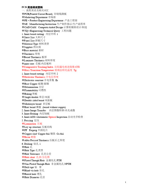
PCB英语培训资料一. 流程英语及相关词汇❖PCB(Printed Circuit Board) 印制线路板❖Marketing Department市场部❖PE – Product Engineering Department 产品工程部❖MI - Manufacturing Instruction生产制作指示/生产流程单❖CAD/CAM - Computer Aided Design计算机辅助设计/制造❖TQ—Engineering Technical Query 工程问题1. Inner board cutting: 内层开料-1❖Sheet Size大料尺寸❖Panel Size拼板尺寸❖Material Type材料类型❖Supplier供应商❖Base material基材❖Thickness厚度❖Board Thickness板厚❖Laminate Thickness材料厚度❖inner core 芯板/内层板料❖Comparative Tracking Index 比较漏电痕迹指数CTI❖Glass Transition Temperature玻璃态转化温度Tg1. Inner board cutting: 内层开料-2❖Dielectric Thickness介电层厚度❖Dielectric constant介电常数Er❖Base Copper底铜/基铜❖Delamination分层❖Flammability可燃性❖Baking烘板❖Single/double单层/双面❖Double sided board双面板❖Multilayer board 多层板❖Bare board裸板(board without copper)2. Inner Image Transfer:内层图像转移/内光成像3. Inner Etching 内层蚀板4. Inner AOI—Automatic Optical Inspection自动光学检查5. Pressing 层压❖Lamination 压板❖Lay-up structure压板结构❖PP - Prepreg半固化片❖Copper clad/ Copper foil铜箔Cu foil❖Resin树脂❖After Pressed Thickness压板后之厚度6. Drilling 钻孔-1❖Hole孔❖Hole Type孔类型❖Hole Tolerance 孔径公差❖Hole chart 孔表/分孔图❖Plated Though Hole 金属化孔PTH❖Non-Plated Though Hole 非金属化孔NPTH❖Drill tape钻带❖Blind via hole盲孔❖Buried hole埋孔❖Hole Diameter孔径6. Drilling 钻孔-2❖Hole location孔位❖Hole Position Tolerance孔位误差❖Hole Position Deviation孔位置偏差❖2nd Drilling 重钻❖Mounting hole安装孔❖Pin hole销定孔❖Target Hole目标孔❖Slot 槽,坑❖No. of holes孔数❖Laser via hole激光穿孔❖Roughness粗糙度7. Plate Through Hole (PTH)沉铜/孔化❖Hole wall copper thick 孔壁铜厚❖Defect缺陷❖Cracking裂缝8. Outer Dry Film 外层干菲林/外光成像-1❖Dry Film干菲林/干膜D/F❖External layer外层❖Internal layer内层❖Component Side 零件面C/S❖Solder Side焊接面S/S❖Top side/ layer 顶层❖Bottom side/layer底层❖Primary side首面❖Secondary side第二面❖(提示: 层的写法尽量按客户的习惯书写)8. Outer Dry Film 外光成像-2❖Power plane电源层❖Ground 接地层❖Layer层❖Dry-film tenting D/F封孔❖Surface mounting Device表面粘贴装置SMD❖Line Width线宽—LW❖Line Space线隙—LS: Line-Line/Line-Pad/Pad-Pad❖Conductor导体❖Circuit线路❖Pattern线路❖Artwork菲林❖Master drawing菲林图形❖Artwork Modification菲林修改❖Outer Dry Film外光成像-3❖Annular ring锡圈❖Min.Annular Ring最小环宽/焊盘宽❖Hole breakout 破环/崩孔❖Pad焊盘❖Round pad圆盘❖Teardrop泪珠❖Clearance/space间距/间隙❖Minimum 最小---Min.❖Maximum 最大---Max.❖Min.Spacing between Line to Line线与线间的最小距离❖Test coupon图样❖Registration Deviation 对位偏差9. Pattern Plating 线路电镀/图形电镀❖Plating电镀❖Chemical corrosion化学腐蚀❖Copper plating电镀铜❖Copper thickness on hole wall 孔内铜厚❖Max.Board Thickness After Plating电镀后总板厚度之上限10. Outer Etching 外蚀板❖Undercut侧蚀11. Solder Resist 湿绿油/阻焊-1❖S/M(Solder Mask) 阻焊❖Solder resist film阻焊菲林❖SM print SM印油菲林❖SM imaging SM曝光菲林❖Solder Mask opening 阻焊开窗/曝光窗❖Solder Mask material/Type 绿油材料/类型❖Color颜色❖Shiny有光泽的,发光的(光亮油,)❖Matte哑光油的❖Matte Green 哑光绿油❖Liquid Photo-Imaginable (LPI)液态光固化剂11. Solder Mask 湿绿油/阻焊-2❖W/F(Wet Film) 湿膜/湿绿油❖Ball Grid Array (BGA) 球栅阵列❖S/M Bridge 绿油桥❖Cover 盖(油入孔)❖Tenting封孔/盖油❖Via Plugging 封孔❖Plug Hole塞孔❖Filled with solder resist 塞孔❖Solder mask on bare copper (SMOBC) 裸铜覆盖阻焊膜❖Encroach 侵占, 蚕食❖Encroach into holes 入孔12. Carbon Ink 印碳油❖Carbon ink碳油❖Carbon Resistance 碳油电阻13. Component Mark 印字符❖Silk Screen丝印❖Component Marking 元件字符C/M❖Legend字符❖Corner mark板角记号❖Logo标记❖Date Code周期代号❖Cust. P/N: customer part number客户型号❖Revision/Version:版本号14. Gold Finger Plating 金手指❖Bevelling斜边❖Gold Finger(G/F) 金手指❖Chamfer倒角❖Key slot槽孔❖Au/Ni 金/镍15. Hot Air Leveling 喷锡❖HAL(Hot Air Leveling) 热风整平❖HASL Hot Air Solder Leveling❖Impedance阻抗IMP❖Surface Treatment表面处理16. Immersion Silver 沉银17. OSP抗氧化处理18. Immersion Tin 沉锡19. Immersion Gold/Imm Au 沉金20. Solder/Tin/Lead Stripping 退锡❖ENIG----Electroless Nickel/Immersion Gold 沉金(工艺) ❖Ag银21. V-Cutting V-坑❖V-Cut V - 坑❖Remain Thickness 保留厚度❖Scoring==V-CUT刻槽❖Scratch划痕❖V-groove V- 坑22. Routing (铣/锣板)/ Punching 啤板❖Profiling外围成型❖Engineering drawing工程图纸❖Fiducial mark基准点❖Dimension尺寸❖Length 长度❖Width 宽度❖Breakaway tab/area板边位❖Datum hole基准参考孔❖Punching die /Punch 啤模❖Offset偏移量❖Outline外形❖Shape 外形23. Electrical Testing 电测试❖E-test fixture E-T 夹具❖Electrical Test Fixture电测试夹具❖V oltage电压❖Open/short开路/短路❖Probe point测试点24. Outer Final QC 最后检查❖Warpage翘曲度❖Bow and twist 板弯曲25. Peelable Mask 印蓝胶❖Peelable Mask/Blue Mask蓝胶❖Peelable可剥性26. Packing&Shipment 包装出货❖Vacunm Pack真空包装❖No.of Pcs Per Bag每包数量❖Packing包装27. Other其它相关-1❖Gerber Data 客户资料打包文件❖Checklist检查表❖production film 生产菲林❖Paste film粘贴/贴键菲林/钢网❖Solder coating上锡❖Reliability可靠性❖Assembly安装性❖Correspondance符合性❖Pin gauge 针规❖Backplane背板❖Customer客户27. Other其它相关-2❖Customer P/N客户产品编号❖Delivery交货❖Description说明❖Golden board金板❖Missing 缺少❖Mother board 主机板❖Ionic cleanliness离子清洁度/离子污染度❖Location位置❖Max. X-out坏板上限/最大允许报废板数❖No.of Array/Panel每个拼板套板数❖Negative反面的❖Positive正的27. Other其它相关-3❖Production生产板❖Sample样板❖Remark备注❖Special requirement特殊要求❖Specification详细说明,制作规范❖Wiring线路❖Square方形的❖View From…观察方向由…❖Lead free process 无铅处理❖Dummy Pad 为圆形或方形的PAD(加在板边位/标位或空白处起平衡电镀作用)❖Dummy copper实心的铜皮❖Thermal Pad 散热盘❖Fibre纤维面二. 问题之基本模式❖Title: Engineering technical question of 021D2002R2 (JOVE P/N: 20LN21119)==On Hold/Go on with suggestion❖Hello Ye jian,❖Nice to contact with you! I'm Jack, an Engineer from Engineering department in Jove.❖For the captioned project, we found some questions need you to confirm with customer.❖Question 1: As there are PTH (plated-hole) between the edge of unit, after doing V-cut, the holes will be scratched, and after customer divide them into two parts along the v-cut line, the copper showing in A part on the hole wall and that on the board may be picked off, which will lead to solder failure. Please refer to fig01❖Suggestion: a)To avoid this potential fault, we will modify the cad data: to add two PTH holes as position B to insure the connection between top and bottom sides. And to add two NPTH holes as position C (use 2nd drill) at the end-point of V-cut line which closed to that big PTH hole to cut the copper off so as to avoid copper being picked off. Please kindly confirm this modification can be acceptable.❖b) Or we will do sample board to let our customer to approve. Please have one, a) or b)? ❖Question 2: Same case as question 1 except that the PTH holes is only on one edge of unit. Please refer to fig02❖Suggestion: a) We will do them NPTH holes and will shave the copper around holes to get about 8 mil clearance.❖ b) We only add two NPTH holes (use 2nd drill) at the end-point of V-cut line whichclosed to that big PTH hole to avoid that potential fault. Please kindly confirm these modification can be acceptable.❖❖Have a nice day!❖B.Regards❖Ding, you de**********************❖Engineering technical question of 021D2002R2 (JOVE P/N: 20LN21119)==On Hold/Go on with suggestion❖Dear John(名字)❖Hello Mr Smith(姓)❖Hi Miss Green❖Nice day John❖Good Morning Jack❖Nice to contact with you! / I’m glad to cooperate with you!❖I'm Jack, an Engineer from Engineering department in Jove.❖1) After checking the captioned new project/updated gerber data, we have some questions as below. Would you please help to settle them. 在检查完此新板后,我们有如下问题。
- 1、下载文档前请自行甄别文档内容的完整性,平台不提供额外的编辑、内容补充、找答案等附加服务。
- 2、"仅部分预览"的文档,不可在线预览部分如存在完整性等问题,可反馈申请退款(可完整预览的文档不适用该条件!)。
- 3、如文档侵犯您的权益,请联系客服反馈,我们会尽快为您处理(人工客服工作时间:9:00-18:30)。
PCB专业英语培训教材
Training Department (QJ)
NOV. 2006
制作人:邓玲娟(Sopheya)
TOPSEARCH
前言
•What is PCB?
Printed Circuit Board(印刷线路板)
•PCB Effect?
Conduct Electricity (导电) Transmission Signel(传输信号) Supported Fixation Action(支撑固定)
IQC
Incoming process Quality Control
Final Quality Control
Quality Assurance
QA MKT IPQC
Marketing
FQC
TOPSEARCH
Manufacturing Engineering Production Production Engineer Production Material Control Management Information System
TOPSEARCH
• Administration & Maintenance A&M (行政及维修部) • Human Resources HR (人力资源部) • Research & Development R & D (研究及发展部) • Purchasing and Shipping P & S (采购及船务部) • Account ACC (财务部) • Training Department TR (培训部) • Management Information System MIS (资讯系统部 ) • Process Engineer PE (工序工程部)
目录
一、Department Introduction 部门介绍
二、Process Flow 工艺流程
三、Test
TOPSEARCH
一.Department Introduction
(部门介绍)
• Incoming Quality Control IQC (来料检查) • Incoming process Quality Control
TOPSEARCH
• FQC • QA • MKT • PMC • ME • PROD • IQC • IPQC
市场部 计划部 来料检查 生产过程品质控制 制作工程部 生产部 品质控制部 品质保证部
TOPSEARCH
• A&M • HR • R&D • P&S • ACC • TR • MIS
•行政及维修部 •研究及发展部 •财务部 •培训部 •采购及船务部 •人力资源部 •资讯系统部
IPQC (生产过程品质控制)
• Final Quality Control FQC(品质控制部) • Quality Assurance QA (品质保证部 ) • Marketing MKT(市场部 ) • Production Material Control PMC(计划部 ) • Manufacturing Engineering ME (制作工程部) • Production PROD (生产部 )
TOPSEARCH
Administration & Maintenance 行政及维修部
Human Resources
人力资源部
Research & Development
研究及发展部
Purchasing and Shipping
采购及船务部
Account
财务部
Training Department
Output 出货
Outer Etching 外层蚀板
Inner Etching 内层蚀刻
Profiling 成型
Black Oxide 黑氧化
MultiBond\Brown Oxidation 棕化
E-test 开/短路测试 )
Pressing 压板
Packing 包装
Drilling 钻孔
Plated-through hole 沉铜<孔金属化>
PE PROD PMC ME MIS
TOPSEARCH
二、工艺流程
TOPSEARCH
Board Cut (界料)
Inner Dry
Film (内层干菲林)
Gold TAB 镀金手指
Hot Air
Leveling 喷锡
Surface Treatment 表面处理
Component Mark 白字
Wet Film 绿油<湿菲林>
TOPSEARCH
Inner Dry Film Outer Dry Film Inner Etching outer Etching Inner Inspection Outer Inspection
TOPSEARCH
3.PCB Sort:
A:Single-sided\Doublesided\Multi-layer Printed Circuit Board (PCB)
单面/双面/多层PCB
B:Rigid PCB Flexible PCB Flex-rigid PCB
刚性/挠性/刚挠性PCB
TOPSEARCH
Pattern
Plating 图形电镀
Outer Dry Film 外层干膜
TOPSEARCH
PCB Process Code
PCB工序代码
BD-CUT PTH ODF PF E-Test
IDF IET DR PS PP OET SF C\M Packing
In-Ins MB\BO Out-Ins WF Output
Production Material Control
Manufacturing Engineering
Production Process Engineer
来料检查 生产过程品质控制
品质控制部 品质保证部 市场部
计划部
制作工程部 生产部 工序工程部
TOPSEARCH
connection
Incoming Quality Control
培训部
Management Information System
资ห้องสมุดไป่ตู้系统部
TOPSEARCH
Incoming Quality Control Incoming Process Quality Control Final Quality Control Quality Assurance
Marketing