金红石型TiO2能带图-态密度图
Materials Studio在材料模拟中的应用——以TiO2晶体为例

广东化工2019年第19期·34·第46卷总第405期Materials Studio在材料模拟中的应用——以TiO2晶体为例贾涛,张佳媛,罗柔,张晋梅,白雪(成都师范学院化学与生命科学学院,四川成都611130)[摘要]二氧化钛具有三种主要的晶型,金红石型,锐钛矿型和板钛矿型,三种晶型的结构不同,因此性质也不同。
本文将使用Materials Studio 中的CASTEP程序对二氧化钛三种晶型进行模拟,并测量不同晶型中体系的能带结构和态密度。
[关键词]Materials Studio;二氧化钛;能带结构;态密度[中图分类号]TQ[文献标识码]A[文章编号]1007-1865(2019)19-0034-02Materials Studio Application in Material Simulation—Take TiO2Crystal As anExampleJia Tao,Zhang Jiayuan,Luo Rou,Zhang Jinmei,Bai Xue(College of Chemistry and Life Science,Chengdu Normal University,Chengdu611130,China)Abstract:Titanium dioxide has three main crystal types,rutile type,anatase type and plate-titanium type.The three crystal types have different structures and therefore different properties.CASTEP in this article will use the Materials Studio program of titanium dioxide,to simulate the three kinds of crystal and measuring different crystal type system in the band structure and density of states.Keywords:materials studio;titanium dioxide;band structure;density of states随着材料科学的不断发展与进步,研究者们对材料的探索程度更加深入,但传统的研究方法难以高效地对材料进行分析研究,而且传统的研究方法误差更大,难以及时的向研究者反馈实验数据。
TiO2的介绍
TiO2又名钛白粉,白色粉末,无毒,不溶于水、有机酸和弱无机酸,微溶于碱。
在浓硫酸以及氢氟酸长时间煮沸可完全溶解,在1800o C以上逐渐熔融。
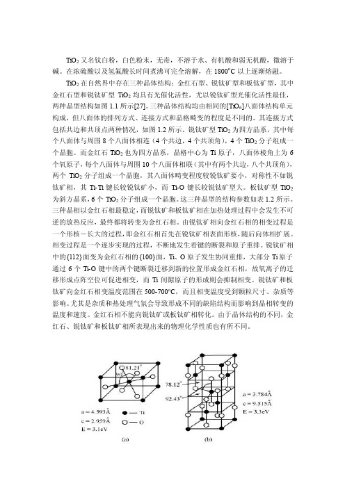
TiO2在自然界中存在三种晶体结构:金红石型、锐钛矿型和板钛矿型,其中金红石型和锐钛矿型TiO2均具有光催化活性,尤以锐钛矿型光催化活性最佳,两种晶型结构如图1.1所示[27]。
三种晶体结构均由相同的[TiO6]八面体结构单元构成,但八面体的排列方式、连接方式和晶格畸变的程度是不同的。
其连接方式包括共边和共顶点两种情况,如图1.2所示。
锐钛矿型TiO2为四方晶系,其中每个八面体与周围8个八面体相连(4个共边,4个共顶角),4个TiO2分子组成一个晶胞。
而金红石TiO2也为四方晶系,晶格中心为Ti原子,八面体棱角上为6个氧原子,每个八面体与周围10个八面体相联(其中有两个共边,八个共顶角),两个TiO2分子组成一个晶胞,其八面体畸变程度较锐钛矿要小,对称性不如锐钛矿相,其Ti-Ti键长较锐钛矿小,而Ti-O键长较锐钛矿型大。
板钛矿型TiO2为斜方晶系,6个TiO2分子组成一个晶胞。
这三种晶型的结构参数如表1.2所示。
三种晶相以金红石相最稳定,而锐钛矿和板钛矿相在加热处理过程中会发生不可逆的放热反应,最终都将转变为金红石相。
由锐钛矿相向金红石相的相变过程是一个形核-长大的过程,即金红石相首先在锐钛矿相表面形核,随后向体相扩展。
相变过程是一个逐步实现的过程,不断地发生着键的断裂和原子重排。
锐钛矿相中的{112}面变为金红石相的{100}面,Ti、O原子发生协同重排,大部分Ti原子通过6个Ti-O键中的两个键断裂迁移到新的位置形成金红石相,故氧离子的迁移形成点阵空位可促进相变,而Ti间隙原子的形成则会抑制相变。
锐钛矿和板钛矿向金红石相变温度范围在500-700o C,而且相变温度受到颗粒尺寸、杂质等影响。
尤其是杂质和热处理气氛会导致形成不同的缺陷结构而影响到晶相转变的温度和速度。
二氧化钛常见的三种晶体结构
二氧化钛常见的三种晶体结构
二氧化钛在自然界中有三种主要的晶体结构,分别是金红石型、锐钛型和板钛型。
其中,板钛型是不稳定的晶型,它在650℃以上的温度下会转化为金红石型,因此在工业上没有实用价值。
1. 金红石型:这是二氧化钛最稳定的结晶形态。
它的结构致密,与锐钛型相比有较高的硬度、密度、介电常数与折光率。
金红石型的晶体细长,呈棱形,通常是孪晶;而锐钛型一般近似规则的八面体。
由于其单位晶格由两个二氧化钛分子组成,所以它具有较大的稳定性和相对密度,因此具有较高的折射率和介电常数及较低的热传导性。
2. 锐钛型:这种晶型在常温下是稳定的,但在高温下会向金红石型转化。
其转化强度视制造方法及煅烧过程中是否加有抑制或促进剂等条件有关。
一般认为在165℃以下几乎不进行晶型转化,超过730℃时转化得很快。
以上内容仅供参考,如需获取更多信息,建议查阅二氧化钛相关的书籍或咨询化学专家。
钛白粉的性质

物理性质
相对密度 熔点和沸点 介电常数 电导率 硬度 吸湿性 热稳定性
相对密度
在常用的白色颜料中,二氧化钛的相对密度最小,同 等质量的白色颜料中,二氧化钛的表面积最大,颜料 体积最高。
表 常见白色颜料的相对密度
颜料名称 锐钛型二氧化钛
ห้องสมุดไป่ตู้
相对密度/(g/cm3) 3.8~3.9
饱和Na2CO3溶 液
饱和K2CO3溶 液
300
钛白粉元素,能溶于氢氟酸,生成氟钛酸,其 反应方程式如下: TiO2 + 6HF ==== H2TiF6 + 2H2O 在长时间煮沸的情况下,溶于浓硫酸,生成硫 酸钛或硫酸氧钛,其反应方程式如下: TiO2 + 2H2SO6 ==== Ti(SO4)2 + 2H2O TiO2 + H2SO6 ==== TiOSO42 + H2O
根据可见光谱长范围400~700nm,所以理想 的二氧化钛粒径应0.2~0.5μm,但是人们的视 觉总认为蓝白色比纯白色更白,因此都倾向于 生产0.2μm粒径左右的二氧化钛,从这一点来 讲消除金红石型二氧化钛固有黄相是有可能的。 从图5-12可以看出0.2μm的小粒径比0.3μm的 大粒径能反射更多的蓝光和绿光而显得更白。 表5-7为二氧化钛在不同波长下的最佳粒径。
曲线表明R型二氧化钛 对蓝色、绿色和红色光 线的相对散射能力为为 二氧化钛粒子大小的函 数。在0.2μm处,各波 长光线散射的总和就增 至最大。当离子增加至 0.25~0.30μm之间时, 蓝色光线的散射迅速减 少,但绿色和红色光线 的散射却相对地不变。 在0.15μm处对于蓝色光 线的最大散射,光谱中 红色和绿色范围内的光 线散射就显著下降。
金红石型TiO_2点缺陷性质的第一性原理研究_冯庆
文章编号:1000 0364(2008)05 1096 05金红石型T iO2点缺陷性质的第一性原理研究冯 庆1,2,王新强1,刘高斌1(1.重庆大学数理学院,重庆400044; 2.重庆师范大学物理系,重庆400046)摘 要:本文运用基于局域密度泛函和赝势的第一性原理方法研究了金红石相T iO2点缺陷的电子性质,结果表明氧空位缺陷使晶体的费米能量升高,在能隙中没有产生杂质能级.钛空位缺陷使晶体的费米能量降低,并在价带顶部产生了一个杂质能级,与价带顶能量相差约0.4eV.本文还计算了金红石相T iO2在具有氧空位和钛空位点缺陷情况下的键长变化、态密度和电荷布居状况.关键词:金红石;T iO2;点缺陷;第一性原理中图分类号:O469 文献标识码:AFirst principles study of point defects in rutile TiO2FENG Qing1,2,WANG Xin Qiang1,LIU Gao Bin1(1.College of M athematics and Physics,Chongqi ng University,Chongqing400044,China;2.College of Physics,Chongqing Normal U niversity,Chongqing400046,China)Abstract:Point defects in TiO2in rutile phase are investigated by using first principles pseudopotential calcu lations based on density functional theory(DFT).By comparing w ith perfect crystal,it is found that in the case of oxygen vacancy Fermi energy goes up and no defect level appears in the gap and in the case of titanium v acancy Fermi energy goes down and a defect level appears in the gap,w hich is about0.4eV above the top of v alue band.The bond length,density of states and population of TiO2w ith oxygen vacancy and titanium va cancy have also been analy zed in this paper.Key words:rutile,T iO2,point defects,first principles theory收稿日期:2008 07 12基金项目:重庆自然科学基金(CST C,2006BB415)作者简介:冯庆(1978-),男,重庆人,讲师,在读博士,师承王新强教授,从事半导体功能材料研究.E mail:fengq-126@1 引 言T iO2是一种n型金属氧化物半导体,是一种具有良好物理化学性质的多功能材料.TiO2具有金红石、锐钛矿和板钛矿三种晶型,纯净的TiO2呈白色,自然界中以红色或金黄色形式存在.金红石T iO2是一种宽带隙半导体,能隙大小达到3.1eV.近年来在实验方面,TiO2通过溶胶 凝胶[1]、溅射[2]、化学气相沉积[3,4]等制备方法在气敏传感器[5]、太阳能电池、光催化涂层、电容器及亲水材料等方面有着广泛应用,并且前景非常广阔.在理论分析方面,也通过不同的近似方法对锐钛矿[6]、金红石[7]的表面结构性质[8]、杂质[9]、缺陷、晶体 气体表面的反应性质以及基于氧化钛的产物[10,11]有不同的模拟计算.由于半导体的诸多性质取决于价带顶和导带底的电子状态以及其中的载流子分布,因此带隙的大小、能带极值的对称性和电子密度分布便成为半导体材料最关注的问题之一.点缺陷,特别是空位点缺陷是三维周期性晶体最常见的一种缺陷形式,对材料的宏观特性起着重要的作第25卷 第5期原 子 与 分 子 物 理 学 报Vo l.25 N o.5 2008年10月JOU RNA L OF A T OM IC AN D M OLECUL AR PHYSICS Oct.2008用.在通常的生长条件下,二氧化钛的氧是不足的,以TiO2-x的形式存在,X的典型数值是小于0 008,T iO2的相变图表明有Magneli相存在, M ag neli相既是指组成为T i n O2n-1,n=4~6 的非化学计量系数比的锐钛矿相或金红石相.材料中的缺陷及缺陷结构决定了这种非化学计量比的T iO2的光学、电学性质.氧空位将引起对分子的吸附,所以对点缺陷中电子结构的研究,将对理解T iO2材料的特性起重要的作用.本文将利用基于密度泛函理论的第一性原理方法,对金红石型TiO2的点缺陷进行研究,探讨点缺陷对电子状态密度分布、能带结构、布居数分布的影响,为研究提供理论依据.2 计算方法本文采用M S中的CASTEP软件包进行计算,其计算步骤概括为三部:首先建立周期性的目标物质的晶体;其次,对建立的结构进行优化,这包括体系电子能量的最小化和几何结构稳定化;最后是计算性质,包括体系能量、电子密度分布,能带结构和电子布居分析等.CASTEP是基于局域密度泛函理论(DFT),离子实与价电子之间相互作用采用赝势处理.由于引入了缺陷,需要构造超级晶胞并使用周期性边界条件.超级原胞必须足够大,才能忽略缺陷之间的相互作用.我们通过从超级原胞中取出一个氧(钛)原子的办法来构造氧(钛)空位缺陷.具体参数设置如下:平面波的截断能量为300eV,迭代过程中的收敛精度为0.2 10-5eV/原子,最大迭代循环次数为100次,方法选用LDA,定域泛函选用CA PZ形式,图1为金红石相T iO2的初始原胞,对结构参数的优化计算与实验值符合得很好,如表1所示,实验与理论的误差小于1%,由于局域密度泛函理论的缺陷使带隙宽度有所低估.由于周期性边界条件的引入,超级原胞的大小对计算结果影响很大,如果直接在一个1 1 1的原胞中引入空位杂质缺陷,那么相当于T iO2-x中X等于0.5,这样的计算结果无太大实际研究和应用意义,原因是首先杂质与杂质之间的距离不能忽略,杂质之间的相互关联影响将会使计算结果超过误差极限,其次这种办法引入杂质使掺杂浓度过高,无实际指导意义.因此本文采用8个原胞48个原子组成的2 2 2的超级原胞,一方面是考虑到计算机的计算能力,另一方面,在这种情况下,点缺陷距离为6 ,其相互作用基本可以忽略,相当于TiO2-x中X等于0.0625 (即Ti8O15).图1 金红石相T iO2初始原胞结构示意图F ig.1 T he structure of rut ile T iO2primitive cell表1 金红石T iO2单原胞晶格常数与能隙宽度T ab.1 T he lattices parameters and ener gy gapof r utile T iO2unit cella( )b( )c( )E g ap(eV) Exp. 4.594 4.594 2.959 1.9T heory 4.587 4.587 2.954 3.03 结果与分析图2是含有一个氧空位的T iO2金红石相2 2 2晶体结构示意图,氧空位位置如箭头所示,费米能量为7.374eV.图3是标准金红石相的TiO2单元胞和含有一个氧空位T iO2金红石相的2 2 2晶体结构的能带示意图.从图中可以看出费米能级周围的能带结构,由于氧空位杂质缺陷的引入,在导带底出现了一条能带(箭头所示),这条能带非常靠近费米面,优化后可以看出费米面并未进图2 含有一个氧空位的T iO2金红石相2 2 2晶体结构示意图F ig.2 T he2 2 2supercell structur e of rutile T iO2w ith one oxy gen vacancy1097第5期 冯庆等:金红石型T iO2点缺陷性质的第一性原理研究图3 2 2 2原胞的金红石T iO 2晶体能带结构(a)含一氧空位有几何优化;(b)含一氧空位无几何优化;(c)无氧空位F ig.3 T he band structur e of rutile T iO 2with one ox yg en vacancy in 2 2 2super cell(a)one oxygen vacancy with geometry opti m i zation,(b)one oxygen vacancy without geometry optimizati on,(c)w i thout oxygen图4 金红石相T iO 2-0.06252 2 2晶体结构中氧空位周围原子几何位置分布图Fig.4 T he relaxed geometr y around t he ox ygen vacancyin 2 2 2super cell of rutile T iO 2-0.0625入导带.该结构使禁带宽度有所降低,材料的导电性能加强,并影响到T iO 2的电子和光子性质.该点所处的势是三个钛原子围绕着一个氧空位,这条相对平直的能带反应出局域点缺陷状态.对比表2和表3可以看出对于含有一个氧空位的单原胞金红石相TiO 2的电荷布居分布情况的变化,在单原胞内缺少一个氧时,钛的电正性有所减弱,氧位置的电荷布居数有所增加,Ti O 键的电荷布居数最大有0.11个电荷的减少,各键长变化在表3中都有所标明.2 2 2的超级原胞优化迟豫后原子位置及键长变化变化趋势如图4所示,圆圈代表空位,箭头标明近邻原子的移动变化趋势,可以看出,近邻氧原子有靠拢氧空位的趋势,而近邻钛原子则是有远离氧空位的趋势.说明空位周围的正电荷不能充分束缚电子,并且能带的位置与近邻的T i 原子密切相关,优化计算各健长发现,空位周围的Ti 原子将屏蔽氧空位的正电荷.这种能带位置的移动将随所选取的超级原胞的增大而向上移动.表2.表3对单原胞的Ti O 各健长和电荷布居进行了分析,研究空位的引入对键长及电荷分布的影响,发现一个氧空位的引入,O 原子周围的电负性增强而T i 原子周围的电正性减弱,氧空位最近邻两类的T i 原子的电荷布居数从1.23变化到0.86和1.02,而对于2 2 2的标准晶体结构的充分迟豫优化后费米能量为5.76eV,含有氧空位的TiO 2与标准的T iO 2相比,费米能量增加了1.62eV.表2 金红石相T iO 2单原胞键长与电荷布居分析T able 2 T he bo nd length and population analysisof rutile T iO 2unit cellSpecies Ion s p d f Total Charge O 1 1.84 4.770.000.00 6.61-0.61O 2 1.84 4.770.000.00 6.61-0.61O 2 1.84 4.770.000.00 6.61-0.61O 3 1.84 4.770.000.00 6.61-0.61Ti 1 2.29 6.34 2.140.0010.77 1.23Ti22.29 6.342.140.0010.771.23Bon dPopulation Length( )O(002) T i(002)0.77 1.94865O(001) T i(002)0.77 1.94865O(004) T i(001)0.77 1.94865O(003) T i(001)0.77 1.94865O(004) T i(002)0.26 1.98025O(003) T i(002)0.26 1.98025O(002) T i(001)0.26 1.98025O(001) T i(001)0.26 1.98025O(001) O(002)-0.07 2.53639O(003) O(004)-0.07 2.53639O(001) O(004)-0.10 2.77824O(001) O(003)-0.10 2.77824O(002) O(004)-0.10 2.77824O(002) O(003)-0.102.778241098原 子 与 分 子 物 理 学 报 第25卷表3 含有一氧空位金红石相T iO 2单原胞键长与电荷布居分析T able 3 T he bond leng th and populat ion analysis of rutileT iO 2unit cell wit h one ox ygen vacancySpecies Ion s p d f Total Charge O 1 1.84 4.800.000.00 6.65-0.65O 2 1.84 4.800.000.00 6.65-0.65O 3 1.83 4.760.000.00 6.59-0.59T i 1 2.26 6.51 2.370.0011.140.86T i22.29 6.392.290.0010.891.02BondPopulation Length( )O(003) T i (001)0.66 1.87766O(002) T i (002)0.71 1.97957O(001) T i (002)0.71 1.97955O(001) T i (001)0.33 1.96286O(003) T i (002)0.28 1.86299O(002) T i (001)0.33 1.96286O(001) O(002)-0.08 2.57222O(002) O(003)-0.09 2.69678O(001) O(003)-0.092.69677图5 金红石相T iO 22 2 2晶体结构的态密度F ig.5 T he partial and total density of rutile T iO 2in 2 2 2supercell w ithout vacancy图5和图6是2 2 2晶体结构的金红石T iO 2态密度分布情况,图5是不含氧空位的,而图6是含有一个氧空位的,从图中可以看出,价带顶主要是氧的2p 电子的贡献,而导带底主要是钛的3d 电子的贡献.在引入一个氧空位后,费米能级接近于导带,说明这是一种典型n 型的TiO 2.导带的占据状态的分布遍及整个超级原胞,通过分析导带的占据情况得出结论,氧空位附近的多余电子的主要贡献在价带,引起价带布居的变化.图6 含一个氧空位的金红石相T iO 2-0.06252 2 2晶体结构的态密度F ig.6 T he partial and total densit y of rutile T iO 2-0.0625in 2 2 2supercell w ith one o xyg en vacancy图7 2 2 2晶体结构中含有一个钛空位的金红石相T i 1-0.0625O 2能带结构F ig.7 T he band str ucture of rut ile T i 1-0.0625O 2w ith onetitanium vacancy in 2 2 2supercell图7为有一个钛空位TiO 2金红石相2 2 2晶体结构的能带结构,相当于Ti 1-x O 2中的X 等于0.0625,费米能级下移动,已进入了价带,这是明显的一种p 型杂质形式.计算过程足够迟豫,掺杂而引起了半导体载流子,统计发生巨变的一个重要判据是费米能级与许可带的能距大小.如果EF 与EC 十分靠近,甚至进入了许可带,那么电子的密度高得使相互之间的泡利排斥不可忽略.这与金属电子类似,是载流子简并的情况.在价带顶上方出现了由于钛空位引入而产生的受主能级,其位置约在费米能级上方0.4eV,这一能级将产生很高的载流子浓度.图8显示一个钛空位TiO 2金红石相1099第5期 冯庆等:金红石型T iO 2点缺陷性质的第一性原理研究图8 金红石相T i1-0.0625O22 2 2晶体结构中钛空位周围原子几何位置分布图Fig.8 T he relaxed geometry around the titanium vacan cy in2 2 2supercell of rutile T i1-0.0625O2的2 2 2晶体结构迟豫计算后各键长和各原子位置的变化情况,从图中可以看出,钛空位周围的氧原子都有远离该钛空位的趋势,也就是说明钛空位附近显示出局域的电负性,排斥周围的氧原子远离该区域,体系的费米能量为4.37eV,比无缺陷的2 2 2晶体结构降低了1.39eV.4 结 语本文利用基于局域密度近似和超软赝势的方法,研究了金红石相T iO2点缺陷性质.对金红石相T iO2具有氧空位和钛空位点缺陷情况下的能带结构、键长变化、态密度和电荷布居状况进行模拟计算分析,计算采用8个原胞48个原子组成的2 2 2原胞的晶体结构,发现在含有一个氧空位时,费米能量为7.374eV,与标准的T iO2相比,费米能量增加了1.62eV.在导带底出现了一条能带,且非常靠近费米面,T i-O键的电荷布居数最大有0.11个电荷的减少,近邻氧原子有靠拢氧空位的趋势,而近邻钛原子则是有远离氧空位的趋势.从电荷布居数分析来看,价带顶主要是氧的2p电子的贡献,而导带底主要是钛的3d电子的贡献.在引入一个氧空位后,费米能级接近于导带,说明这是一种典型n型的T iO2.对于有一个钛空位TiO2金红石相2 2 2原胞的晶体结构模拟计算表明费米能级下移动,已进入了价带,明显是一种p型杂质形式,在价带顶上方出现了由于钛空位引入而产生的受主能级,其位置约在费米能级上方0.4 eV,这一能级将产生很高的载流子浓度.充分迟豫计算后发现,钛空位周围的氧原子都有远离该钛空位的趋势,而费米能量为4.37eV,比无缺陷的2 2 2超级原胞降低了1.39eV.参考文献:[1] Garzella C,Comini E,T empesti E,et al,T iO2thinfilms by a nov el sol g el processing for gas sensor application[J].Sens.A ctuator s B,2000,68:189.[2] Chow L L W,Yuen M M F,Chan P C H.Reactivesputter ed T iO2thin films humidity sensors wit h negative substrate bias[J].Sens.A ctuator s B,2001,76:310.[3] Kang B C,Lee S B,Boo J H.Gr owth of T iO2thinfilms on Si(100)substrates using single molecular precursors by metal or ganic chemical vapor deposition[J].S ur f.Coat.T echnol.,2000,131:88.[4] Wu R J,Sun Y L,Lin C C,et al,Composite o f T iO2nano wires and nafion as humidity sensor material[J].Sens.A ctuator s B,2006,115:198[5] Skubal L R,M eshkov N K,et al.Detection and identification of gaseous or ganics using a T iO2sensor[J].J.Photo.Photo.A,2002,148:103[6] N a P hattalung S,Smith M F,K wiseon K im,et al.First pr inciples study o f native defects in anatase T iO2[J].Phys.Rev.B,2006,73:125205[7] Cho E,Han S.First Principles study of point defects inrutile T iO2-x[J].Phys.Rev.B,2006,73:193202;M urugan P,Belosludov R V,M izuseki H,et al.Electro nic and mag netic properties of double impuritiesdoped T iO2(rut ile):first principles calculat ions[J].J.A p p l.Phys.,2006,99:08M105[8] P illay D,Hwang G S.O2 coverage dependent CO oxidation on reduced T iO2(110):a first pr inciples study[J].J.Chem.Phys.,2006,125:144706[9] Y u Bai,Q iang Chen.N dopant induced ant iferro magnetism in anatase T iO2:first pr inciple study[J].SolidS tate Commun.,2008,147:169[10] Xue W D,Cai J.F irst principle study on SrT iO3filmo xyg en imperfection[J].J.A t.M ol.Phy s.,2007,24(4):875(in Chinese)[薛卫东,蔡军.Sr T iO3薄膜氧缺陷的第一性原理研究[J].原子与分子物理学报,2007,24(4):875][11] Li C X.First pr inciple study on the structural andelectronic pr operties o f middle small size CdS and CdT eclusters[J].J.A t.M ol.Phys.,2007,24(5):1060(in Chinese)[李春霞.中小尺寸CdS和CdT e团簇结构与电子性质的第一性原理研究[J].原子与分子物理学报,2007,24(5):1060]1100 原 子 与 分 子 物 理 学 报 第25卷。
金红石型二氧化钛(110)黄金纳米表面的稳定性

STM characterization of size-selected V 1,V 2,VO,and VO 2clusters on a TiO 2(110)-(1×1)surface at room temperatureScott P.Price,Xiao Tong,Claron Ridge,Vladimir Shapovalov,Zhenpeng Hu,Paul Kemper,Horia Metiu,Michael T.Bowers,Steven K.Buratto ⁎Department of Chemistry and Biochemistry,University of California,Santa Barbara,CA 93106-9510,USAa b s t r a c ta r t i c l e i n f o Article history:Received 1November 2010Accepted 22February 2011Available online 2March 2011Keywords:VanadiumVanadium oxide Titanium oxideScanning tunneling microscopy ClustersSurface structure,morphology,roughness,and topographyWe use ultra-high vacuum scanning tunneling microscopy (UHV –STM)to probe,at the atomic level,the structure of mass-selected isolated V 1,V 2,VO and VO 2clusters deposited on rutile TiO 2(110)by ion soft landing.All four species interact differently with the TiO 2surface and the ultimate binding site and con figuration strikes a balance between the gas-phase structure and the ligation of this cluster by the TiO 2surface.Our results show that vanadium atoms prefer to bind in the upper threefold hollow sites on the surface and have a slight tendency to pair along the [1–10]direction,while vanadium dimers bind to the surface oriented along the [001]direction exclusively.VO clusters bind with the vanadium atom in the upper threefold hollow site and with the oxygen atom bound to an adjacent fivefold coordinated Ti atom (5c-Ti).The VO 2cluster also binds with the vanadium atom in the upper threefold hollow site and with both oxygen atoms bound to adjacent 5c-Ti atoms or with only one oxygen bound to the surface and the other directed out of the plane of the surface.©2011Elsevier B.V.All rights reserved.1.IntroductionVanadium oxide particles supported on TiO 2are known to catalyze a number of reactions including the selective oxidation of methanol to formaldehyde [1,2].Detailed understanding of the composition of the active vanadia and the interaction between the vanadia and the titania support are important in providing an atomistic model for the catalytic properties of this system.To this end,a number of model catalyst studies have been carried out both experimentally [3–14]and theoretically [14–19].Madix and coworkers have prepared submo-nolayer films of catalytically active vanadium oxide on TiO 2by hydrolysis of VOCl 3in UHV [4,5].Subsequent characterization of these films by XPS mainly showed vanadium in its 5+oxidation state,but details regarding the structure of the clusters proved dif ficult given the size distribution [4].Another approach adopted by several groups is to grow submonolayer vanadia films by evaporative deposition of vanadium metal in an oxygen-rich environment and/or post-oxidation of deposited vanadium clusters in an oxygen atmosphere [6–11].A mixture of vanadium oxidation states was observed,with the vanadium being more highly oxidized after annealing in higher background pressures of oxygen [8–11].Again,atomic level-modelswere not possible,given the distribution in size and composition of the clusters.Scanning tunneling microscopy (STM)has also been used to provide direct visualization of vanadium and vanadia particles on single crystal CeO 2(111)[8,9]and TiO 2(110)-(1×1)[11–13].For vanadium atoms and small VO x clusters deposited on CeO 2(111),Freund and coworkers showed that the V atoms bind to the upper threefold hollow site.Slight oxidation of the vanadium produced isolated VO and small clusters of VO x (i.e.VO 2and VO 3)arranged with a vanadyl V=O bond directed out of the plane of the surface [8,9].Submonolayer films of metallic vanadium were deposited on TiO 2(110)-(1×1)by evaporative deposition from a vanadium source [12,13],while oxides were generated by either reactive evaporation or post-oxidation [11].In these experiments,a variety of cluster sizes and morphologies was found,indicating that a mixture of vanadia cluster compositions was deposited.This mixture made it dif ficult to pinpoint the exact number of vanadium and oxygen atoms in a cluster,which is crucial information for determining any atomistic model.In an effort to gain a more detailed understanding of these model catalysts,we deposit mass-selected V x and V x O y clusters on rutile TiO 2(110)-(1×1)in ultra high vacuum (UHV).Size-selection allows us to control the exact composition of the vanadium and vanadia clusters.The cluster-decorated surfaces (~0.01ML coverage)are then characterized using STM in order to determine the adsorption site and geometry of each particular vanadium or vanadia cluster.Additional insight is gained by comparing these results with previously reported DFT structures [15,16].This comparison allows us to build a detailed structural model of the various vanadium and vanadium oxide particles on TiO 2(110).Surface Science 605(2011)972–976⁎Corresponding author.Tel.:+18058933393;fax:+18058934120.E-mail address:buratto@ (S.K.Buratto).0039-6028/$–see front matter ©2011Elsevier B.V.All rights reserved.doi:10.1016/j.susc.2011.02.016Contents lists available at ScienceDirectSurface Sciencej o ur n a l h o m e p a g e :ww w.e l s ev i e r.c o m/l o c a t e /s u s c2.ExperimentalThese experiments were carried out in a UHV apparatus with a base pressure below1×10−10Torr.TiO2(110)samples(Commercial Crystal Laboratories)were cleaned in UHV with several cycles of argon ion bombardment(1kV)and annealing(~1200K for10s).Sample cleanliness was verified by STM.Immediately prior to deposition, samples wereflashed to~1000K for several seconds to ensure that surface hydroxyls were removed.The apparatus used to generate size-selected vanadium and vanadium oxide clusters has been described previously[20]and only details relevant to these experiments are described here.The second harmonic output of a pulsed yttrium aluminum garnet(YAG)laser is focused onto a rotating,translating vanadium rod,which generates a plasma of ablated vanadium atoms.A pulse of argon is introduced into the source,resulting in plasma reactions that cause vanadium and vanadium oxide cluster growth.Positive ions are extracted,accelerated, and focused using several steering lenses before being size-selected by a magnetic-field analyzer.The ions can then be collected on a movable plate detector,where mass spectra and kinetic energy distributions for the ion beam are recorded by measuring the ion current.A mass spectrum of the vanadium ion beam is shown in Fig.1a.Seeding the argon expansion gas with20%oxygen yields an ion beam composed of V x O y+ions,as shown in the mass spectrum in Fig.1b.This mass spectrum agrees well with previous reports of positively-charged vanadia ion beams produced by laser ablation[21,22].Clusters are deposited on the TiO2(110)substrate by moving the ion detector out of the path of the ion beam and then focusing and steering the beam towards the sample,which is housed in the UHV deposition chamber.During deposition,the TiO2sample is positively biased at a voltage equal to the average ion kinetic energy that was measured on the detector.This allows the clusters to be soft-landed with incident kinetic energy between0and3eV/atom.Measuring the ion current on the sample during deposition provides an upper-bound estimate of the expected vanadium or vanadia coverage.In each of our experiments, 0.01–0.05ML of size-selected vanadium clusters was deposited, assuming a sticking probability of unity.Monolayer coverage is defined as one vanadium atom per TiO2unit cell.Samples are characterized using STM,and the actual cluster coverage is determined from analysis of the STM data.STM imaging is carried out at room temperature using a sample bias of+1.3to+2.1V and a constant tunneling current of 0.2nA.Most STM images were recorded within20min to several hours following deposition,however,samples were also imaged for several days after deposition with no significant changes in the density or appearance of the clusters.3.Results and discussion3.1.Size-selected vanadium clusters on TiO2(110)-(1×1)STM characterization of a clean TiO2(110)-(1×1)surface shows an array of alternating bright and dark stripes,which correspond to rows offivefold coordinated Ti atoms(5c-Ti)and bridging oxygen atoms, respectively[23].STM images recorded after depositing V1+are presented in Fig.2a and b.The bright spots that appear on the rows are vanadium atoms.A large-area image(Fig.2a)shows that the V1 atoms bind to the TiO2surface with no preference for step edge sites and do not form large three-dimensional clusters.The low mobility and monodisperse size of these clusters indicates that the monomers do not sinter.This result was also observed for evaporatively deposited vanadium[12,13]and was attributed to the highreactivityIonCurrent(nA)400300200100Mass (amu)1.51.00.50.0IonCurrent(nA)Mass (amu)(a)(b)Fig.1.(a)Mass spectrum(0–400amu)of V xclusters produced using an argon expansiongas,(b)mass spectrum(0–400amu)of V x O y clusters generated using an expansion gasof20%oxygen seeded in argon.Peaks are labeled in the form(x,y),where x and ycorrespond to the number of vanadium and oxygen atoms,respectively,that are presentin the cluster.Fig.2.(a)Large-area and(b)high-resolution STM images of V1clusters on TiO2(110).In thehigh-resolution image,the circled cluster is an individual vanadium monomer,while thecoffee-bean shaped feature(labeled with a square)is a pair of monomers along the[1–10]direction.(c)Top-view model showing the binding site of a single vanadium monomer onthe titania surface.This is also the lowest-energy DFT structure calculated for V1on TiO2inRef.[15].(d)Top-view model of a pair of vanadium monomers exhibiting the coffee-beanstructure.In these models,the silver,red,and green spheres correspond to titanium,oxygen,and vanadium atoms,respectively.The labels O Br and5c-Ti denote the locations ofthe bridging oxygen andfivefold coordinated titanium rows,respectively,in the model.973S.P.Price et al./Surface Science605(2011)972–976of vanadium with the titania surface[12].The vanadium monomers appear slightly elongated(~9Å)in the[001]direction and are1.7Åin height,indicating that the features are one atomic layer tall[12,13]. The elongation of vanadium clusters along the[001]direction of the TiO2(110)surface has also been observed by Agnoli and coworkers, where vanadium clusters appeared10–15Ålong[12].The high-resolution image of Fig.2b shows two types of features:isolated V atoms(marked with a circle)and coffee bean-shaped structures formed by pairs of vanadium monomers aligned along the[1–10] direction(marked with a square).These are the only types of features that resulted from the deposition of vanadium atoms.All isolated V1features(depicted within the circle of Fig.2b)are positioned between the5c-Ti and bridging oxygen rows.This is consistent with the structural model proposed by Asaduzzaman and Kruger[15]in which the vanadium atoms are bound to the upper threefold hollow sites between the5c-Ti and bridging oxygen rows.A model showing the binding of a V atom to this site is shown in Fig.2c. This assignment is also consistent with previous STM results where the vanadium was deposited using an evaporation source[12].The bonding of the vanadium to these three oxygen atoms,coupled with DFT calculations showing that the vanadium atom transfers electrons to its neighboring oxygen atoms[15],suggests that this electronic effect is responsible for the observed elongation of the vanadium clusters in our work and in the work of Agnoli et al.[12].For pairs of V1atoms oriented along[1–10](the coffee-bean shape depicted within the square of Fig.2b),both vanadium atoms are located in upper threefold hollow sites and are separated by a bridging oxygen row,as shown in the model presented in Fig.2d.The distance between vanadium atoms measured by STM is4.0Å,which is~2.3times longer than the V―V bond length ingas-phase V2[24],suggesting that these are two individual V monomers, rather than dimeric vanadium.The coffee bean-like features we attribute to V-atom pairs are similar to those which were previously reported for evaporatively deposited vanadium[12].However,in the work of Agnoli et al.[12],clusters elongated in the[001]direction were also observed.The fraction of clusters paired along[001]is small but significant.Statistical analysis carried out in the work of Agnoli,et al.showed that81%of the observed clusters were single monomers,15%were pairs of atoms along[1–10], and4%were pairs of atoms along[001][12].Excluding the features paired along[001],84%of the clusters were isolated and16%exhibited the coffee-bean structure.In our experiments,we observe a different distribution of features.Upon deposition of size-selected vanadium monomer,a statistical analysis of21images similar to that shown in Fig.2a exhibits a distribution where45%of the features are isolated monomers and55%of the features are pairs of atoms along[1–10]. Based on our observed coverage of~0.01monolayer,we would expect very few pairs of clusters to appear randomly.Clearly,the vanadium monomers have a greater tendency to pair along[1–10]in the present study.We attribute this to the mobility of the V atoms due to their excess kinetic energy(between0and3eV)upon impact with the surface.It is important to note that the pairing of the vanadium monomers in this way was not predicted by DFT calculations discussed in the work of Asaduzzaman and Kruger[15].In the work of Asaduzzaman and Kruger [15],the vanadium monomers were predicted to repel one another due to their high positive charges resulting from electron transfer into the surface.Clearly the experimental data of Fig.2and Agnoli,et al.[12]do not confirm this prediction,but instead suggest a propensity for the monomers to pair along the[1–10]direction.This pairing implies that the magnitude of electron transfer from the vanadium atoms to the surface is much smaller than predicted by DFT calculations.Fig.3a shows a large-area image of V2+clusters deposited on titania. Again,clusters are distributed evenly across the terraces,with no preference for a specific type of adsorption site.The high-resolution image presented in Fig.3b indicates that the V2clusters are symmetrically positioned over the bridging oxygen rows.This is the only shape and binding site observed for V2clusters in our experiments.The V2clusters appear as ovals of length~13Åalong[001]and height of 1.7Å.The deposited V2cluster is completely different than the two-atom clusters that form after deposition of size-selected V1.The obvious differences between the V2clusters on the TiO2(110)surface and the two types of features observed for V1atoms on the surface indicate that these two species bind differently to the surface.Based on these STM observations,we propose that the vanadium dimer is oriented along a bridging oxygen row as shown in Fig.3c.The cluster is located between two bridging oxygen atoms with both vanadium atoms bound to their respective nearest-neighbor bridging oxygen atom.It is interesting to note that the images of the V2in Fig.3b clusters have a very similar appearance to the paired clusters oriented along [001]that resulted from the evaporative deposited of vanadium onto titania in the work of Agnoli,et al.[12].Since we only see pairs of V atoms oriented along the[1–10]direction and since we only see V dimers oriented along[001]direction,Agnoli,et al.,most likely have a mixture of V1and V2emanating from their evaporation source.This is consistent with the work of Kant,et al.,which has shown that dimers are readily formed in vanadium effusion sources[25].Additional work by the Armentrout group has also shown that large vanadium clusters break up preferentially into vanadium dimers upon exposure to reactive gas[26],a result that supports dimer emission from an evaporative source.The presence of dimeric vanadium emanating from effusion sources provides a further explanation for the difference in the relative concentration of coffee-bean features in our work(where100%of the clusters in the mass selected source are V1)compared to the work of Agnoli,et al.3.2.Size-selected vanadium oxide clusters on TiO2(110)-(1×1)Fig.4a shows an STM image of the titania surface after deposition of size-selected VO+.As with V2,VO remains intact upon adsorption,does not sinter,and binds to the TiO2surface without any preference for step-edge sites.A higher resolution image(Fig.4b)indicates that these clusters are positioned between the titanium and bridging oxygen rows. The asymmetric positioning of the cluster suggests that the vanadium atom in the VO cluster is bound to a threefold hollow site,similar tothe Fig.3.(a)Large-area and(b)high-resolution STM images of V2clusters supported on TiO2(110).(c)Top-view model showing a V2cluster bound to the TiO2surface.Silver,red, and green spheres correspond to titanium,oxygen,and vanadium atoms,respectively.974S.P.Price et al./Surface Science605(2011)972–976binding site for vanadium atoms,and the oxygen atom binds to a 5c-Ti atom making the cluster planar.A top-view model and a three-dimensional side-view model showing the binding of the cluster to the titania surface are shown in Fig.4c and d,respectively.It is interesting to note that this model is identical to the lowest-energy DFT structure for VO on TiO 2,as described by Shapovalov,et al.[16].The VO clusters have a length of 10Åin the [001]direction and are 1.7Åtall.Although the height of the VO cluster is the same as that of a V monomer,the VO cluster is slightly longer along [001].The elongation of the VO cluster is attributed to the binding of the oxygen atom to a 5c-Ti,as shown in the model in Fig.4c.Fig.5a shows a large-area image of VO 2clusters deposited on titania.The high-resolution image presented in Fig.5b indicates that the VO 2clusters are asymmetrically positioned over the 5c-Ti rows.The VO 2cluster is 1.7Åtall and 14Ålong in the [001]direction.The only observed difference between VO and VO 2clusters on TiO 2(110)is the degree of elongation along [001],which is much greater for the VO 2clusters.Based on this,we constructed a model (Fig.5c and d)showing the binding of a VO 2cluster to the titania surface.In this model,the vanadium atom (green)is positioned in the upper threefold hollow site and both oxygen atoms (dark blue)are bound to neighboring 5c-Ti atoms.This was also calculated to be a low-energy structure using DFT.Although the lowest-energy DFT structure for VO 2on TiO 2(110)involves the vanadium atom sitting in an upper threefold hollow site with one oxygen atom bound to a neighboring 5c-Ti atom and the other oxygen pointing out of the plane of the surface [16],this structure is only 0.25eV lower in energy than that presented in the model in Fig.5c and d.The height of the cluster and elongation along [001]indicates that the slightly higher-energy structure in the DFT calculations [16]is observed experimentally.These results differ somewhat from those reported by Agnoli and coworkers for reactive evaporation and post-oxidation vanadia depositions.Reactive evaporation mainly yielded vanadia clusterswhich were symmetrically positioned over the 5c-Ti rows.These clusters varied in length along [001],leading the authors to suggest that both monomeric and dimeric vanadia were formed [11].It is reasonable that vanadia monomers and dimers would be observed after reactive evaporation,considering the evidence we have outlined here suggesting that a mixture of metallic monomer and dimer clusters are emitted from the effusion source.Post-oxidation resulted in a variety of features;some clusters were symmetrically positioned over the 5c-Ti rows,while others were still located between the Ti and bridging oxygen rows.This result was attributed to incomplete oxidation of the vanadium during the post-oxidation [11].Because DFT calculations suggest that VO 3is formed when a V-decorated TiO 2surface is exposed to oxygen [16],it is possible that the clusters positioned symmetrically over the 5c-Ti rows in Agnoli,et al.,are VO 3and other highly oxidized species (including dimers).The clusters which are located between the Ti and bridging oxygen rows following post-oxidation are likely a mixture of V,VO,VO 2,and dimers with low oxygen content.This is supported by XPS evidence showing that post-oxidation results in a variety of vanadium oxidation states [3,10].4.ConclusionsWe have deposited size-selected V 1,V 2,VO,and VO 2clusters on TiO 2(110)and determined their preferred adsorption sites using STM.V 1,VO,and VO 2clusters are centered asymmetrically over the 5c-Ti rows and have varying lengths along the [001]direction where the length of V 1b VO b VO 2.V 2clusters appear symmetrically positioned over the bridging oxygen parison of the STM results to DFT calculations has allowed us to determine an atomistic model for these structures.Performing STM studies on size-selected clusters has allowed us to determine that evaporative deposition of vanadium results in a mixture of monomers and dimers,while reactive evaporation andpost-Fig.4.(a)Large-area and (b)high-resolution STM images of VO clusters supported on TiO 2(110).(c)Top-view and (d)side-view models showing the binding site of the VO cluster on the titania surface.The silver and light blue spheres correspond to titanium atoms,red spheres are oxygen atoms,the green sphere is a vanadium atom,and the dark blue sphere is the oxygen atom in the VO cluster.The model shown in (c)and (d)is also identical to the lowest-energy DFT structure for VO on TiO 2from Ref.[16].Fig.5.(a)Large-area and (b)high-resolution STM images of VO 2clusters deposited on TiO 2(110).(c)Top-view and (d)side-view models showing the binding site of a VO 2cluster on the titania surface.The silver and light blue spheres correspond to titanium atoms,red spheres are oxygen atoms,the green sphere is vanadium,and the two dark blue spheres are the oxygen atoms in the VO 2cluster.The model presented in (c)and (d)is also a low-energy DFT structure for the VO 2/TiO 2system.975S.P.Price et al./Surface Science 605(2011)972–976oxidation methods for preparing thin vanadiafilms likely results in a mixture of cluster compositions.AcknowledgementsThis work was supported by the National Science Foundation (CHE-079489).References[1]I.E.Wachs,Catalysis Today100(2005)79.[2] B.M.Weckhuysen,D.E.Keller,Catalysis Today78(2003)25.[3]J.Biener,M.Baumer,R.J.Madix,Surface Science432(1999)178.[4]Q.G.Wang,R.J.Madix,Surface Science474(2001)L213.[5]Q.G.Wang,R.J.Madix,Surface Science496(2002)51.[6]G.S.Wong,D.D.Kragten,J.M.Vohs,Surface Science452(2000)L293.[7]G.S.Wong,D.D.Kragten,J.M.Vohs,The Journal of Physical Chemistry.B105(2001)1366.[8]H.L.Abbott,A.Uhl,M.Baron,Y.Lei,R.J.Meyer,D.J.Stacchiola,O.Bondarchuk,S.Shaikhutdinov,H.J.Freund,Journal of Catalysis272(2010)82.[9]M.Baron,H.Abbott,O.Bondarchuk,D.Stacchiola,A.Uhl,S.Shaikhutdinov,H.J.Freund, C.Popa,M.V.Ganduglia-Pirovano,J.Sauer,Angewandte Chemie.International Edition48(2009)8006.[10]G.S.Wong,M.R.Concepcion,J.M.Vohs,Surface Science526(2003)211.[11]S.Agnoli,M.Sambi,G.Granozzi,C.Castellarin-Cudia,S.Surnev,M.G.Ramsey,F.P.Netzer,Surface Science562(2004)150.[12]S.Agnoli,C.Castellarin-Cudia,M.Sambi,S.Surnev,M.G.Ramsey,G.Granozzi,F.P.Netzer,Surface Science546(2003)117.[13]J.Biener,M.Baumer,J.Wang,R.J.Madix,Surface Science450(2000)12.[14]H.S.Kim,S.A.Zygmunt,P.C.Stair,P.Zapol,L.A.Curtiss,Journal of PhysicalChemistry C113(2009)8836.[15] A.M.Asaduzzaman,P.Kruger,Journal of Physical Chemistry C112(2008)4622.[16]V.Shapovalov,H.Metiu,Journal of Physical Chemistry C111(2007)14179.[17]H.Y.Kim,H.M.Lee,R.G.S.Pala,H.Metiu,Journal of Physical Chemistry C113(2009)16083.[18]H.Y.Kim,H.M.Lee,H.Metiu,Journal of Physical Chemistry C114(2010)13736.[19]P.C.Redfern,P.Zapol,M.Sternberg,S.P.Adiga,S.A.Zygmunt,L.A.Curtiss,TheJournal of Physical Chemistry.B110(2006)8363.[20]P.Kemper,A.Kolmakov,X.Tong,Y.Lilach,L.Benz,M.Manard,H.Metiu,S.K.Buratto,M.T.Bowers,International Journal of Mass Spectrometry254(2006)202.[21]R.C.Bell,K.A.Zemski,D.R.Justes,A.W.Castleman,The Journal of Chemical Physics114(2001)798.[22]R.C.Bell,K.A.Zemski,K.P.Kerns,H.T.Deng,A.W.Castleman,The Journal ofPhysical Chemistry.A102(1998)1733.[23]U.Diebold,Surface Science Reports48(2003)53.[24]ngridge-Smith,M.D.Morse,G.P.Hansen,R.E.Smalley,A.J.Merer,TheJournal of Chemical Physics80(1984)593.[25] A.Kant,S.S.Lin,The Journal of Chemical Physics51(1969)1644.[26] C.X.Su,D.A.Hales,P.B.Armentrout,The Journal of Chemical Physics99(1993)6613.976S.P.Price et al./Surface Science605(2011)972–976。
金红石型二氧化钛的价带电子结构表征(110)-(1 - 2)
Valence band electronic structure characterization of the rutile TiO 2(110)-(1×2)reconstructed surfaceC.Sánchez-Sánchez a ,b ,M.G.Garnier c ,P.Aebi c ,M.Blanco-Rey d ,P.L.de Andres a ,d ,J.A.Martín-Gago a ,e ,M.F.López a ,⁎aInstituto Ciencia de Materiales de Madrid (ICMM-CSIC),C/Sor Juana Inés de la Cruz 3,28049-Madrid,Spain bInstituto de Ciencia de Materiales de Sevilla (ICMSE-CSIC),Américo Vespucio 49,41092-Sevilla,Spain cDépartement de Physique and Fribourg Center for Nanomaterials,Universitéde Fribourg,CH-1700Fribourg,Switzerland dDonostia International Physics Center,Universidad del País Vasco UPV/EHU,Paseo Manuel de Lardizábal 4,20018Donostia-San Sebastián,Spain eCentro de Astrobiologia (CSIC-INTA),28850Madrid,Spaina b s t r a c ta r t i c l e i n f o Article history:Received 31May 2012Accepted 28September 2012Available online 6October 2012Keywords:Titanium oxideElectronic structure ARUPS DefectsThe electronic structure of the TiO 2(110)-(1×2)surface has been studied by means of angular resolved ultraviolet photoemission spectroscopy (ARUPS).The valence band dispersion along the high symmetry sur-face directions,[001]and [1–10],has been recorded.The experimental data show no dispersion of the band-gap Ti 3d states.However,the existence of dispersive bands along the [001]direction located at about 7eV below the Fermi level is reported.The existence of two different contributions in the emission from the defects-related state located in the gap of the surface is univocally shown for the first time.©2012Elsevier B.V.All rights reserved.1.IntroductionMetal oxides are of great importance due to their use in several technological applications such as heterogeneous catalysis,photo-chemistry,sensors,and composite materials [1].Among all of them,titanium dioxide has become the prototype for surface science studies due to its ordered structure and its capability of conduction upon re-duction.One of the main areas of application of TiO 2is the field of ca-talysis,being nowadays one of the more widely used materials for catalytic supports.In order to better understand and improve its cat-alytic properties,a detailed knowledge of its electronic structure is of crucial importance.The rutile TiO 2(110)is the most stable face and,in this work,we shall focus on its electronic properties.This surface,upon sputtering and annealing under ultra-high vacuum (UHV)con-ditions,presents the well-known (1×1)structure corresponding to the bulk truncated structure,modi fied by simple but relevant surface relaxations [2].The stable (1×1)surface transforms into a long range ordered structure with (1×2)symmetry upon further reduction of the sub-strate [3].The quality of this new surface depends on the reduction level of the TiO 2crystal,on the annealing temperature achieved dur-ing sample preparation,and on the duration of the annealing.This surface reconstruction has been the subject of many investigations during the last years.Most of the scienti fic efforts have been devotedtowards the determination of the geometrical disposition of atoms.This has been a matter of controversy,as several atomic models have been proposed based on different experimental techniques and theoretical calculations [4–9].In a previous work carried out by our group,the (1×2)structure was elucidated from density functional theory (DFT)calculations and quantitative low-energy electron diffraction experiments [LEED-I(V)][10,11].Similar to Onishi's proposal,a Ti 2O 3stoichiometry on the sur-face was favored,although some structural differences between these two models were reported.Surprisingly,not many investigations have focused on the electronic structure of the (1×2)surface reconstruction.One signi ficant issue in the study of TiO 2is the presence of defects of different nature,which are typical of this kind of substrates.Its importance arises from the fact that the presence of these defects,hy-droxyl impurities,oxygen atom vacancies and interstitials Ti atoms,confer unusual properties to this material.The local character of these defects makes near-field scanning probe microscopy a crucial technique for their study,although its assignation is not always clear and straightforward [12–18],not only regarding the surface to-pography but also from the electronic point of view.Depending on the amount of defects,some can be also detectable by spectroscopic techniques.The oxidation state of titanium cations in stoichiometric (110)TiO 2corresponds nominally to Ti 4+.However,an important contribution of defects will be originated when the surface is reduced by annealing and/or ion bombardment.The presence of these defects,not only mainly oxygen vacancies but also,in a lower amount,inter-stitials Ti 3+atoms,on the TiO 2(110)surface will lead to an excess ofSurface Science 608(2013)92–96⁎Corresponding author.Tel.:+34913349081;fax:+34913720623.E-mail address:m flopez@icmm.csic.es (M.F.López).0039-6028/$–see front matter ©2012Elsevier B.V.All rights reserved./10.1016/j.susc.2012.09.019Contents lists available at SciVerse ScienceDirectSurface Sciencej o u r na l h o me p a g e :ww w.e l s e v i e r.c o m /l o c a t e /s u s celectrons at these specific sites.This residual charge is expected to be transferred to the Ti atoms located close to defects[19–21].Consequently,the trapped electron will partially populate the Ti3d orbitals and will change the oxidation state of the adjacent Ti cations from4+to3+.For this reason,when the defects contribu-tion is high,a new electronic state appears in the gap region below EF. This state is referred in ultraviolet photoemission spectra as band-gap or defects-related state and it has been the subject of many spec-troscopic studies[22,23].Since the TiO2(110)-(1×2)surface recon-struction is obtained from the(1×1)surface by annealing at high temperature,a significant amount of defects are originated in this process.Thus,a clear enhancement of the Ti3+band-gap state is expected for the(1×2)reconstruction[24].Additionally,the presence of surface Ti2O3rows where the Ti cations have a nominal 3+oxidation state will contribute to enhance the emission at the band-gap state.In this paper,the valence band electronic structure of the rutile TiO2(110)-(1×2)surface is investigated by angular resolved ultra-violet photoemission spectroscopy(ARUPS).Special effort has been made to understand the origin of the band-gap state that appears at a binding energy(BE)of approximately0.9eV.We will show that for the(1×2)reconstruction this peak presents a double contribution, one associated to the Ti3+in the Ti2O3rows of the(1×2)reconstruc-tion,and a different one related to the defective Ti3+atoms present throughout the crystal bulk.We also report the presence of a disper-sive band at a BE of about7eV and k//=0.35Å−1.2.Material and methodsExperiments have been carried out in two different ultra-high vacu-um(UHV)chambers,both of them with a base pressure better than 1·10−10mbar.In both cases,a commercial rutile TiO2(110)sample (Mateck)was prepared through repeated cycles of sputtering and annealing at1150K until a sharp(1×1)or(1×2)LEED pattern was obtained.The(1×1)surface is characteristic of a stoichiometric sample or a poorly reduced bulk,while the(1×2)reconstruction is typical of heavily reduced substrates.For the UPS band-gap peak study,three dif-ferent substrates were considered:low,medium and heavily reduced. The criteria used to discern among these three cases have been the color of the sample and the surface structure.In this way,for example, low reduced sample presents a light blue color and a(1×1)surface structure(as observed by STM and LEED).Medium reduced sample is dark blue but still with a(1×1)surface structure.Finally,heavily re-duced sample is almost black and presents a(1×2)surface termination. In all cases the same sample was used,and the degree of reduction was increased by controlling the annealing temperature and the cycle dura-tion.ARUPS measurements were performed using monochromatized He-I radiation from a He discharge lamp in combination with a VG EscaLab Mk II photoelectron spectrometer(20meV resolution),and a sample goniometer for full hemispherical Angular Resolved Photoemis-sion Spectroscopy(ARPES)[25].The angular acceptance and resolution is1°full-cone.Therefore,this corresponds to an approximate kII inte-gration of the Brillouin zone of less than0.04Å−1.Measurements of the band-gap state were done at the UHV chamber located at Centro de Astrobiología(CSIC-INTA),equipped with a hemispherical electron analyzer and a He-I lamp.To perform the ultraviolet photoemission spectroscopy(UPS)analysis the spectra werefitted to a least squares combination of Gaussian components.The background selected for thefitting procedure of the UPS spectra was a linear one as it is the typ-ical used for inelastic backgrounds without a stepwise change in inten-sity,as it was our case.All spectra were recorded at room temperature.The(1×2)reconstructed Ti2O3surface structure was determined from DFT and dynamical LEED in a previous work[10],and the surface model in the present paper has been constructed accordingly.The (1×2)supercell lattice dimensions are a=13.22Å,b=2.99Å,and c=3a,containing a slab of70atoms mirror-symmetric about its middle plane,exposing the Ti2O3reconstruction at both sides(see supplementary information).This ensures that the electronic struc-ture features come only from the bulk and the(1×2)reconstructed surface.The TiO2bulk unit cell dimensions are a=b=4.68Åand c=2.99Å.The plane wave basis has been constructed with a cut-off energy of400eV and a Monkhorst-Pack k-point mesh of7×13×1 (4×4×7for bulk)[26].Energy was converged up to0.01meV/ion and the Fermi level to0.001meV/ion.The supercell height,c,is such that the solid occupies approximately one half of the supercell, which we have shown to be enough to avoid interactions between consecutive slabs.The slab thickness is such that Mulliken charges of atoms in the central Ti–O layer are in good agreement with those of the bulk.The outmost19atoms of both sides of the slab were allowed to relax further with tolerances of0.05eV/Åin the force per atom and 0.001Åin the displacement.Thefinal atomic coordinates differed from those of the previous work[10]by no more than0.04Å.Actual calculations have been performed with the CASTEP code[29].3.Results and discussionFig.1(a)shows a schematic representation of the atomic arrange-ment corresponding to the rutile TiO2(110)-(1×2)surface recon-struction,as derived from previous LEED I(V)and DFT calculations [10].The most protruding features on this surface are the Ti2O3 rows,which extend along the[001]rge gray and small red circles correspond to Ti and O atoms,respectively.Ti3+atoms as-sociated to the surface reconstruction are marked by arrows.The red rectangle of Fig.1(b)represents the surface Brillouin zone(SBZ)for the TiO2(110)-(1×2)termination,with the two high-symmetry di-rections indicated.In this representation also the SBZ for the TiO2 (110)-(1×1)surface is exhibited as a black rectangle.As it can be ob-served,both the(1×1)and the(1×2)surfaces present a rectangular structure in the reciprocal space.Fig.2(a)and(b)exhibits bidimensional representations of the experimental ARUPS spectra corresponding to the rutile TiO2(110)-(1×2)valence band as a function of the momentum parallel compo-nent k II along[001]and[1–10]directions,respectively.In both graphs,the high symmetry points of the SBZ as well as the Fermi sur-face edge are indicated.In the images,the darkest features corre-spond to more intense photoemission peaks while the brightest ones represent the less intense emissions.Along the[001]direction, i.e.the direction of the Ti2O3rows,a convex dispersive band located at a binding energy of about7eV and centered at0.35Å−1can be ob-served.On the other hand,no dispersion is observed along the[1–10] direction,i.e.perpendicular to the reconstruction rows.Previous re-sults on TiO2(110)-(1×1)showed weak dispersion of the states cor-responding to the valence band[27].Fig.2(c)and(d)shows the bidimensional representations of the experimental band-gap state ARUPS spectra along the two high sym-metry directions,[001]and[1–10],respectively.The data indicate that no dispersion can be distinguished by ARUPS.In particular,from Fig.2(c),we conclude there is no significative experimental dispersion of the band-gap state of the(1×2)surface along the direction of the Ti2O3surface wires.This result contrasts with the theoretical pre-diction derived from DFT calculations about the metallic character of the Ti2O3chains along the[001]direction[10].This discrepancy has been associated to the tendency of the GGA functional[30]to overestimate the delocalization of states that may be otherwise local-ized by different factors,like correlation effects and the quasi-1D char-acter of states running along the reconstruction chains.Indeed,the use of GGA+U as an alternative exchange and correlation functional fa-vors the opening of a gap along the[001]direction and results in a dis-persive state in the band gap,localized at the subsurface Ti atoms in the trenches between the Ti2O3chains[31,32].Fig.3shows the com-puted valence band electronic structure for a slab(left)and the corre-sponding projection of bulk states along the GΓ–Z direction(right).93C.Sánchez-Sánchez et al./Surface Science608(2013)92–96Blue dots label states with more than an 80%contribution from atoms of the Ti 2O 3chains,while green dots represent the same for atoms lo-cated on the TiO 2tri-layer closest to the surface.As it is well known,DFT underestimates the band gap because correlation effects are only taken into account in an approximate way (we obtain for bulk TiO 2a band gap of 2eV).Furthermore,the Hohenberg –Kohn theorem applies strictly speaking only to the ground state,and excited states,e.g.in the conduction band,are only covered in an approximate,perturbative way.Finally,the ARUPS technique only provides infor-mation about the valence band.Therefore,we only attempt to com-pare the experimental and theoretical valence bands.In the right hand side panel of Fig.3we show the bands along the G –Z direction from a bulk only calculation (i.e.from the 1×1×1bulk unit cell for TiO 2,as described above).We compare the bulk states from this calcu-lation with the experimental ones in Fig.2a.It is interesting to notice that these states are not affected by the low-dimensional comments made above for the Ti 2O 3chains,and are therefore properly described by a GGA functional.This point is double-checked by performing LDA+U calculations (U=4.5eV);the main effect is a rigid shift of bands by about half an eV to higher binding energies,but no notice-able distortions.The main observed features appear above and below 7eV,similarly as can be seen in the experiment (panel (a)in Fig.2).On the other hand,the states related to the surface (green tri-angles and circles)show a remarkable lack of dispersion very near 7eV.The experimental resolution does not allow seeing this flat surface-like band.For the experimental band structure,a dispersive band similar to the theoretical one happens above and below 7eV,as seen by comparing with Fig.2(panel a).Finally,we notice in Fig.2(c)and (d),that the data exhibit inten-sity maxima at approximately 0.8Å−1(along [001])and 0.15Å−1(along [1–10]).This can be explained by final-state scattering effects,i.e.as an ultraviolet photoelectron diffraction effect (UPD)[28].In order to extract additional information on the band-gap states,UPS measurements for three different reduction levels of the sub-strate have been performed.As it has been mentioned above,it is known that the band-gap state is related to Ti 3+states and it appears after bulk reduction.However,in the case of the (1×2)surface recon-struction,there are also Ti 3+states associated to the Ti 2O 3rows oftheFig.1.a)Schematic representation of the atomic arrangement corresponding to the (1×2)TiO 2(110)surface reconstruction as inferred from DFT calculations (only the last layers are shown).Large (blue)and small circles (red)correspond to Ti and O atoms,respectively.b)Surface Brillouin zone for the TiO 2(110)-(1×2)surface reconstruction marked in red with the two high-symmetry directions [001]and [1–10].The black rectangle corresponds to the extended SBZ for TiO 2(110)-(1×1)surface.Fig.2.Bidimensional representation of the ARUPS spectra of the TiO 2(110)-(1×2)surface as a function of k II along (a)[001]and (b)[1–10]directions for the valence band region,and (c)and (d)for the band-gap states region along [001]and [1–10],respectively.94 C.Sánchez-Sánchez et al./Surface Science 608(2013)92–96surface reconstruction.It is generally accepted that the exact binding energy of an electron depends not only on the level from which pho-toemission originates but also on the oxidation state of the atom and the local chemical environment.Thus,modi fications on the local chemical environment introduce small shifts in the peak position,which are known as chemical shifts.In the present case,two different chemical environments for the Ti 3+ions are present,one at the bulk and another at the Ti 2O 3surface rows.For this reason,these two dif-ferent chemical settings should give rise to different photoemission signals separated by a certain binding energy,making possible their distinction by means of UPS.Fig.4exhibits UPS spectra of the band-gap state region for both a poorly reduced and a highly reduced substrate with a (1×1)surface symmetry,and for a heavily reduced substrate with (1×2)symmetry at the surface.In all spectra,the red solid line through the black data circles represents the result of the least-squares fit,with the blue dashed-dotted component giving the signal corresponding to the low binding energy (BE)peak and the green solid curve showing the high BE emission.The yellow dashed line represents the linear background.As it can be observed in Fig.4(a),for a low reduction level associated to a TiO 2(110)-(1×1)surface,just one peak is needed in order to properly fit the ex-perimental data (chi-square test is 0.079).The binding energy for this peak is 0.78eV with a FWHM value of 0.62eV.If the reduction level isincreased (but still preserving a (1×1)surface)an enhancement of the band-gap state is observed,as it is evident from Fig.4(b).Again,only one peak is necessary to fit the experimental data,being this peak almost identical to the previous one,except for an increase in its intensity.In this case,its binding energy is 0.77eV and the FWHM is 0.63eV (chi-square 0.047).On the other hand,upon further reduction of the substrate a phase transition takes place at the surface,where a new reconstruction appears as it is evidenced from LEED and STM measurements.This new reconstruction,characterized by a Ti 2O 3surface stoichiometry,presents a wider and asymmetric band-gap state peak,which makes necessary the addition of a second com-ponent in the fit.Indeed,for the heavily reduced substrate with a (1×2)surface termination,two contributions have been required to properly fit the band-gap state emission,one located at the same posi-tion as in the previous cases,and another one located at a slightly higher BE (Fig.4(c)).The two curves used in these fits are located at 0.75eV and 1.18eV BE showing a FWHM of 0.67eV and 0.51eV,re-spectively (chi-square 0.077).Attempts to fit this spectrum with a sin-gle component have been unsuccessful due to the asymmetry of the experimental data (best chi-square obtained has been 0.43).This new state appearing together with the (1×2)surface reconstruction and not observed for any of the (1×1)symmetry cases,can only be associated to the Ti 3+states of the Ti 2O 3rows.As it would be expected from the existence of two different chemical environments associat-ed with the Ti 3+states,the UPS experiments clearly indicate the pres-ence of two different contributions in the band-gap state peak:one component is related to the bulk defects typical of the (1×1)structureFig.3.Ab-initio DFT electronic structure calculation along the [001]direction (G –Z).(i)Left panel:band structure of the slab supercell (with the Ti 2O 31×2reconstructed chains).(ii)Right panel:band structure of the 1×1×1bulk TiO 2unit cell projected along the G –Z direction.Red regions in the graph correspond to bulk states with a large weight in the projection along the G –Z direction.Blue and violet correspond to states with small weight and black regions are either gaps or zones with a very small number of states.Green triangles label electronic states that have more than 80%con-tribution from atoms in the Ti 2O 3group,as obtained in the left panel.Green circles label the same corresponding to atoms of the topmost trilayer (TiO 2).Green ellipse marks the dispersive band similar to the experimentalone.Fig.4.UPS spectra of the band-gap states region for:(a)poorly reduced substrate with a (1×1)surface,(b)highly reduced substrate with (1×1)symmetry at the surface,and (c)heavily reduced substrate with a (1×2)symmetry at the surface.95C.Sánchez-Sánchez et al./Surface Science 608(2013)92–96(low BE peak),and the other is due to the Ti atoms present at the sur-face reconstruction in the(1×2)surface(high BE peak).The presence of this new surface termination in the(1×2)TiO2(110)sample sur-face,i.e.the Ti2O3surface rows,is the origin of the sudden appearance of the latter component.It is important to note the increase in the in-tensity of the peak at0.75eV for this sample in comparison to the less reduced ones.The reason of this effect is the increasing amount of Ti3+states not only at the Ti2O3surface rows(peak at1.18eV BE) but also at the bulk(peak at0.75eV BE)when the sample has been reduced.It is worthy to comment on the different contexts for Ti3+and Ti4+ atoms in the(1×2)TiO2(110)sample.The geometrical disposition of the Ti3+atoms at the surface within the Ti2O3chains,and therefore its chemical environment,is completely different to that of the of Ti3+ atoms at the bulk near the defect sites.However,in the case of the Ti4+atoms,the geometrical arrangement in both cases,bulk and surface,is the same.For this reason,no shift in the binding energies should be expected for the surface Ti4+atoms.The possibility of discerning the two components for the band-gap states peak leads to some important consequences.For example,this method based onfitting the bad-gap states region can be used to con-firm the existence and quality level of the(1×2)surface reconstruc-tion on TiO2(110).It could be also used to determine the nature of the interaction of a molecular adsorbate on the(1×2)reconstruction by analyzing the evolution of the relative intensity of the different com-ponents of the band-gap state peak upon deposition.4.ConclusionsIn this paper,the electronic structure of the rutile TiO2(110)-(1×2)surface reconstruction has been characterized,paying special attention to Ti3+related band-gap state.By means of ARUPS,the presence of a downward dispersive band along the rutile TiO2(110)-(1×2)[001]surface direction is determined.This band,with its max-imum at0.35Å−1,appears7eV below the Fermi edge.No dispersion of the band-gap states is observed by ARUPS.Regarding the band-gap states emission,the double nature of this peak has been identified. One component is associated to the Ti3+cations next to the bulk de-fects and the other,observed for the case of the TiO2(110)-(1×2)sur-face reconstruction,to the Ti3+cations in the Ti2O3chains present at the surface.AcknowledgmentsThis work has been supported by the Spanish CYCIT(MAT2011-26534)and the Ministry of Science and Innovation(CSD2007-41 NANOSELECT).C.S.S.gratefully acknowledges Ministerio de Educación for thefinancial support inside the“FPU programme”under the AP2005-0433grant.M.G.G.and P.A.are grateful for the support by the Fonds National Suisse pour la Recherche Scientifique through Div. II and the Swiss National Center of Competence in Research MaNEP. M.B.-R.acknowledgesfinancial support from the Gipuzkoako Foru Aldundia and the European Union7th Framework Programme(FP7/ 2007–2013)under grant agreement no.FP7-PEOPLE-2010-RG276921. Appendix A.Supplementary dataSupplementary data to this article can be found online at http:// /10.1016/j.susc.2012.09.019.References[1]U.Diebold,Surf.Sci.Rep.48(2003)53.[2]W.Busayaporn,X.Torrelles,A.Wander,S.Tomić,A.Ernst,B.Montanari,N.M.Harrison,O.Bikondoa,I.Joumard,J.Zegenhagen,G.Cabailh,G.Thornton,R.Lindsay,Phys.Rev.B81(2010)153404(and references therein).[3]J.Abad,C.Rogero,J.Méndez,M.F.López,J.A.Martín-Gago,E.Román,Surf.Sci.600(2006)2696.[4]P.J.Møller,M.C.Wu,Surf.Sci.224(1989)265.[5]H.Onishi,K.I.Fukui,Y.Iwasawa,Bull.Chem.Soc.Jpn.68(1995)2447.[6] C.L.Pang,S.A.Haycock,H.Raza,P.W.Murray,G.Thornton,O.Gülseren,R.James,D.W.Bullet,Phys.Rev.B58(1998)1586.[7]R.A.Bennett,P.Stone,N.J.Price,M.Bowker,Phys.Rev.Lett.82(1999)3831.[8]K.T.Park,M.H.Pan,V.Meunier,E.W.Plummer,Phys.Rev.Lett.96(2006)226105.[9]N.Shibata,A.Goto,S.-Y.Choi,T.Mizoguchi,S.D.Findlay,T.Yamamoto,Y.Ikuhara,Science322(2008)570.[10]M.Blanco-Rey,J.Abad,C.Rogero,J.Mendez,M.F.Lopez,J.A.Martin-Gago,P.L.deAndres,Phys.Rev.Lett.96(2006)055502.[11]M.Blanco-Rey,J.Abad, C.Rogero,J.Méndez,M.F.López, E.Román,J.A.Martín-Gago,P.L.de Andrés,Phys.Rev.B75(2007)081402(R).[12]uritsen,A.S.Foster,G.H.Olesen,M.C.Christensen,A.Kühnle,S.Helveg,J.R.Rostrup-Nielsen,B.S.Clausen,M.Reichling,F.Besenbacher,Nanotechnology 17(2006)3436.[13]X.Cui,Z.Wang,S.Tan,B.Wang,J.Yang,J.G.Hou,J.Phys.Chem.C113(2009)13204.[14] C.L.Pang,O.Bikondoa,D.S.Humphrey,A.C.Papageorgiou,G.Cabailh,R.Ithnin,Q.Chen,C.A.Muryn,H.Onishi,G.Thornton,Nanotechnology17(2006)5397. [15] C.Sánchez-Sánchez, C.González,P.Jelinek,J.Méndez,P.L.de Andrés,J.A.Martín-Gago,M.F.López,Nanotechnology21(2010)405702.[16] A.Yurtsever,Y.Sugimoto,M.Abe,S.Morita,Nanotechnology21(2010)165702.[17]R.Bechstein,C.González,J.Schütte,P.Jelínek,R.Pérez,A.Kühnle,Nanotechnology20(2009)505703.[18]H.P.Pinto,G.H.Enevoldsen,F.Besenbacher,uritsen,A.S.Foster,Nanotech-nology20(2009)264020.[19]P.Krüger,S.Bourgeois,B.Domenichini,H.Magnan,D.Chandesris,P.Le Fèvre,A.M.Flank,J.Jupille,L.Floreano,A.Cossaro,A.Verdini,A.Morgante,Phys.Rev.Lett.100(2008)055501.[20]M.Nolan,S.D.Elliott,J.S.Mulley,R.A.Bennett,M.Basham,P.Mulheran,Phys.Rev.B77(2008)235424.[21]M.V.Ganduglia-Pirovano,A.Hofmann,J.Sauer,Surf.Sci.Rep.62(2007)219.[22]R.Patel,Q.Guo,I.Coks,E.M.Williams,E.Roman,J.L.de Segovia,J.Vac.Sci.Technol.A15(1997)2553.[23]Z.Zhang,S.Jeng,V.E.Henrich,Phys.Rev.B43(1991)12004.[24]J.Abad,C.Rogero,J.Méndez,M.F.López,J.A.Martín-Gago,E.Román,Appl.Surf.Sci.234(2004)497.[25]T.Pillo,L.Patthey, E.Boschung,J.Hayoz,P.Aebi,L.Schlapbach,J.ElectronSpectrosc.Relat.Phenom.97(1998)243.[26]H.J.Monkhorst,J.D.Pack,Phys.Rev.B13(1976)5188.[27]S.Fischer,J.A.Martín-Gago,E.Román,K.D.Schierbaum,J.L.de Segovia,J.ElectronSpectrosc.Relat.Phenom.83(1997)217.[28]J.Osterwalder,T.Greber,P.Aebi,R.Fasel,L.Schlapbach,Phys.Rev.B53(1996)10209.[29]S.Clark,M.Segall,C.Pickard,P.Hasnip,M.Probert,K.Refson,M.C.Payne,Z.Kristallogr.220(2005)570().[30]J.P.Perdew,K.Burke,M.Ernzerhof,Phys.Rev.Lett.77(1996)3865.[31]V.Celik,H.Unal,E.Mete,S.Ellialtioglu,Phys.Rev.B82(2010)205113.[32]H.Unal,E.Mete,S.Ellialtioglu,Phys.Rev.B84(2011)115407.96 C.Sánchez-Sánchez et al./Surface Science608(2013)92–96。
光学气敏材料金红石相二氧化钛(110)面吸附CO分子的微观特性机理研究
光学气敏材料金红石相二氧化钛(110)面吸附CO 分子的微观特性机理研究∗朱洪强冯庆†(重庆市光电功能材料重点实验室,重庆401331)(重庆师范大学光学工程重点实验室,重庆400047)(2014年2月18日收到;2013年3月17日收到修改稿)利用光学气敏材料吸附气体,引起材料光学性质的变化来测量气体成分,是当前气敏传感研究领域的一个热点方向.本文针对光学气敏材料金红石相TiO2(110)表面吸附CO分子的微观特性进行研究,采用基于密度泛函理论(DFT)体系下的第一性原理平面波超软赝势方法,计算了表面的吸附能、电子态密度、光学性质和电荷密度的变化.结果表明:终止于二配位O原子的TiO2(110)面为最稳定表面,该表面吸附CO分子以C端吸附方式最为稳定,且氧空位浓度越高,越有助于对CO分子的吸附,吸附过程为放热.在氧空位浓度为33%时,吸附能达到1.319eV,吸附后结构趋于更加稳定.表面吸附CO分子后,其实质是表面的氧空位氧化了CO分子,CO分子的电荷向材料表面转移.含有氧空位的表面吸附CO分子后都改善了其在可见光范围内的光学性质,但是氧空位浓度越高,改善其光吸收和反射能力越明显,光学气敏传感特性表现越显著.关键词:光学气敏材料,金红石,CO,密度泛函理论PACS:31.15.A–,71.15.Dx,71.15.Mb,71.15.–m DOI:10.7498/aps.63.1331011引言CO是在燃料燃烧时伴随产生的有毒性气体,少量吸入后就会导致人员伤亡.监测环境中的CO气体通常会用到气敏传感器.目前,电阻气敏传感器运用较为成熟,如SnO2,ZnO等.但电阻气敏传感器远不及光学气敏传感器的灵敏度高,且响应时间也较长.所谓光学气敏传感器,就是利用光学气敏材料吸附气体,引起材料光学性质的改变来检测气体成分及浓度的传感器.因此,对光学气敏材料的研究,成为气体传感器方面新的研究方向和热点领域.金红石相TiO2n型过渡金属氧化物半导体材料(3.0eV[1]).自1972年Fujishi-ma和Honda发现了光照金红石相TiO2电极能分解水后[2],人们对TiO2光催化分解水制氢气[3]、空气环境净化[4,5]、废水处理[6]、光催化[7]以及太阳能电池[8]等领域进行了广泛研究,同时还发现TiO2是良好的光学气敏传感材料,表面结构与材料性能有着紧密联系[9−12].因此,研究金红石相TiO2表面吸附气体引起光学性质的改变,作为检测气体的重要指标,有着极其重要的意义.崔文颖和Simon等人[13,14]运用基于密度泛函理论的第一性原理方法计算优化了金红石TiO2 (110),(001),(101)晶面的几何结构,发现金红石型TiO2(110)晶面为最稳定的吸附面.肖冰等人[15]计算了金红石相TiO2(110)表面性质及STM形态模拟,发现(110)表面的STM形貌凸起部分来自Ti原子,表面存在较多氧空位.CO[16]只在有氧空位的金红石相TiO2(110)表面才会被氧化. Dan[17]和汪洋[18,19]等人也发现CO和NO容易在有缺陷的金红石相TiO2(110)表面吸附,且NO气∗国家自然科学基金(批准号:61274128,61106129)和重庆市自然科学基金(批准号:CSTC2013JCYJA0731)资助的课题.†通讯作者.E-mail:fengq_126@©2014中国物理学会Chinese Physical Society 体在TiO 2(110)面吸附后均以N 2形式脱附.而Linsebigler 等人[20,21]研究了CO 在金红石相TiO 2(110)面吸附,并通过实验和计算得到吸附能大概值.然而,目前对于金红石相TiO 2(110)面吸附CO 分子引起的表面光学性质变化的研究还较少,相应的吸附微观机理的解释还比较缺乏.因此,本文采用基于密度泛函理论(DFT)体系下的第一性原理平面波超软赝势方法,运用CASTEP 软件包模拟计算了光学气敏材料金红石相TiO 2(110)表面吸附CO 分子的情况,对其几何结构、态密度、光学性质、电荷分布等进行分析,为金红石相TiO 2作为光学气敏材料投入实验研究提供理论数据.2模型构建与计算方法金红石相TiO 2属于四方晶系结构,其空间群为P 42/MNM .Burnside 和Labat 等人计算了金红石相TiO 2(110),(100),(001)表面的相对能量,发现金红石相TiO 2(110)相对能量最低[22,23],但表面终止原子不同,稳定性也有所差异.四种表面原子终止结构如图1所示,以A 面能量为基准零点,B,C 和D 面能量相对值为E B =−19.65eV,E C =−32.56eV,E D =−19.76eV,说明终止于二配位O 2c 原子的TiO 2(110)面为最稳定表面(C 面).BADC图1金红石相TiO 2(110)表面不同表面原子终止结构[010][001]100]O 2C (O a )Ti(Ti 6c )Ti(Ti )(a)(b)图2金红石相TiO 2(110)表面优化前后原子结构(a)优化前表面原子结构(b)优化后表面原子结构本文研究采用2×2×3的金红石相TiO 2超晶胞,共9层原子来模拟表面,如图2(a).在Z 方向上建立了10Å的真空层,可忽略其相互作用的影响.优化后,表面原子弛豫,未出现重构,最表层原子仍是二配位的O 2c ,如图2(b)所示.分别建立完整表面、含一个氧空位和含两个氧空位缺陷的金红石相TiO 2(110)表面,其氧空位浓度分别为0%,16.7%和33.3%,CO 分子距离表面初始距离均为0.1665nm,如图3(a),(b),(c),图4(a),(b),(c),图5(a),(b),(c)所示.C O0.1665C O0.3218CO 0.1665CO 0.4336CO 0.1665CO 0.2810(a)(b)(c)(a')(b')(c')图3CO 吸附于完整金红石相TiO 2(110)表面优化前后的原子结构(a)优化前CO 分子O 端垂直吸附;(b)优化前CO 分子C 端吸附;(c)优化前CO 分子水平放置吸附;(a ′)优化后CO 分子O 端垂直吸附;(b ′)优化后CO 分子C 端吸附;(c ′)优化后CO 分子水平放置吸附O C0.1665CO0.166550.0520O CCO0.14760.1665C O0.1427C O(a)(b)(c)(a')(b')(c')图4CO 吸附于一个O 空位缺陷的金红石相TiO 2(110)表面优化前后的原子结构(a)优化前CO 分子O 端垂直吸附;(b)优化前CO 分子C 端吸附;(c)优化前CO 分子水平放置吸附;(a ′)优化后CO 分子O 端垂直吸附;(b ′)优化后CO 分子C 端吸附;(c ′)优化后CO 分子水平放置吸附CO 0.1665C O0.1665C CO 0.0268C O0.1529C0.1665O 0.0484O C(a)(b)(c)(a')(b')(c')图5CO 吸附于两个O 空位缺陷的金红石相TiO 2(110)表面优化前后的原子结构(a)优化前CO 分子O 端垂直吸附;(b)优化前CO 分子C 端吸附;(c)优化前CO 分子水平放置吸附;(a ′)优化后CO 分子O 端垂直吸附;(b ′)优化后CO 分子C 端吸附;(c ′)优化后CO 分子水平放置吸附3结果与讨论3.1吸附微观模型CO分子以O端向下、C端向下和水平放置吸附于完整金红石相TiO2(110)表面的二配位的O2c (O a)顶位,优化后如图3(a′),(b′),(c′)所示.CO分子以不同方式放置吸附于含一个O空位缺陷和含两个O空位缺陷的TiO2(110)表面,优化后分别如图4(a′),(b′),(c′)和图5(a′),(b′),(c′)所示.将三种模型吸附前后的距离归纳于表1,可以发现以下特点:第一,在完整金红石相TiO2(110)表面,不论哪种放置方式,CO分子与表面的距离都出现了增加,说明CO不容易被完整金红石相TiO2(110)表面吸附,有远离表面的趋势.第二,在有氧空位的金红石相TiO2(110)表面,能量优化后,CO分子与表面的距离都出现的缩短,说明在有氧空位的条件下,CO会被TiO2(110)表面吸附.表1CO分子以不同方式放置吸附于金红石相TiO2(110)表面吸附前后距离吸附方式完整金红石表面一个O空位表面两个O空位表面O端吸附吸附前距离/nm0.16650.16650.1665吸附后距离/nm0.32180.14270.1529C端吸附吸附前距离/nm0.16650.16650.1665吸附后距离/nm0.43360.05200.0268水平吸附吸附前距离/nm0.16650.16650.1665吸附后距离/nm0.28100.14760.0484第三,氧空位浓度越大,最终分子与表面距离越短,说明增大氧空位浓度有助于表面对分子的吸附.第四,在有氧空位的表面稳定吸附CO后,C 端吸附距离表面的距离最短,说明其吸附效果优于水平吸附和O端吸附.3.2吸附能CO分子吸附于TiO2(110)表面的吸附能可定义[24]为E ads=(E substrate+E CO)−E(CO+substrate),式中E ads为表面吸附能.E substrate为含有O空位表面晶胞总能量,E CO为吸附前CO分子的能量, E(CO+substrate)为表面吸附CO后整个体系的总能量.本文分别计算了CO分子吸附于完整金红石相TiO2(110)表面、含一个O空位和含两个O空位缺陷表面的吸附能,如表2所示.吸附能为正值说明吸附过程放热,吸附后的结构将趋于更加稳定;反之,吸附能为负值说明吸附过程吸热,吸附后的结构不稳定,吸附不容易实现.从表2中可以看出,CO分子吸附于完整金红石相TiO2(110)表面吸附能均不大于0.2eV,说明吸附不容易实现.当表面出现一个O空位缺陷和两个O空位缺陷时,C端吸附的吸附能分别为0.758 eV和1.319eV,均远远大于水平吸附和O端吸附的吸附能.从吸附能的分析发现:在含有氧空位的表面,Eads(c端吸附)>E ads(水平吸附)>E ads(o端吸附),同样说明金红石相TiO2(110)面吸附CO分子主要以C端吸附方式为主;表面O空位的浓度越高,E ads 越大,说明吸附后结构越稳定,吸附越容易实现.表2CO分子吸附于金红石相TiO2(110)表面的吸附能吸附完整表面吸含一个氧空位表面含两个氧空位表面方式附能E ads/eV吸附能E ads/eV吸附能E ads/eV O端吸附0.2000.0510.019C端吸附0.1820.758 1.319水平吸附0.0710.0970.5163.3表面电子态密度为了进一步研究费米能级附近的电子结构,本文计算了完整、含有两个氧空位缺陷以及CO分子C端吸附于含两个氧空位缺陷金红石相TiO2(110)表面的分态密度和总态密度,费米能级作为零点,如图6所示.501000255075100 /eVD O S /(e l e c t r o n /e V )D O S /(e l e c t r o n /e V )D O S /(e l e c t r o n /e V )/eV/eV图6吸附前后金红石TiO 2(110)表面的态密度可以发现:完整表面费米能级靠近价带顶,导带主要是Ti 3d 轨道和少量O 2p 轨道构成,而价带主要是以O 2p 轨道和少量Ti 3d 轨道的贡献.O 空位缺陷和吸附的CO 分子都属于p 型掺杂,使费米能级靠近导带底.CO 分子吸附于氧空位缺陷表面,在导带底产生了新的杂质能级,该杂质能级是C 2p 轨道的贡献,属于施主能级,在费米能级附近出现新的峰值,改善了TiO 2(110)表面对可见光产生响应的能力.3.4介电函数复介函数ε(ω)=ε1(ω)+i ε2(ω)可以用来描述材料的光学响应函数,其中ε1=n 2−k 2,ε2=2nk .在研究材料的光学性质时,可优先从虚部的介电常数入手,其他性质均可由介电常数作为桥梁,找到对应的联系.根据Kramers-Kronig 色散关系可以得出其实部,同时也可以通过ε1(ω)和ε2(ω)推导得出吸收系数I (ω)和反射率R (ω).与本文计算有关的公式[25]如下:ε1=1+8π2e 2m 2∑V ,C∫d 3k 22π×|e ·M CV (K )|2E C (K )−E V (K )× 3E C (K )−E V (K )− 2ω2,(1)ε2=4π2m 2ω2∑V ,C ∫BZ d 3k 22π|e ·M CV (K )|2×δ[E C (K )−E V (K )− ω],(2)I (ω)=√2ω[√ε21(ω)−ε22(ω)−ε1(ω)]1/2,(3)R (ω)= √ε1(ω)+jε2(ω)−1√ε1(ω)+jε2(ω)+1 2,(4)L (ω)=ε2(ω)ε21(ω)+ε22(ω),(5)其中BZ 为第一布里渊区,C 和V 分别表示导带和价带,K 为倒格矢,|e ·M CV (K )|2为动量跃迁矩阵元,ω为角频率,E C (K )和E V (K )分别为导带和价带上的本征能级.材料对光的响应过程分为吸收过程和反射过程.吸收过程:电子吸收光子能量,从基态跃迁至激发态;反射过程:处于激发态的电子不稳定,会释放能量往低能级跃迁.吸收过程和反射过程与介电函数的虚部和实部对应,即电子吸收光子能量往激发态跃迁的可能性越大,其虚部也将越大;处于激发态的电子释放能量往低能级跃迁的可能性越大,其实部也将越大.图7为吸附前后金红石相TiO 2(110)表面的介电函数图.可以看到,完整金红石相TiO 2(110)表面,其虚部在3eV 后才大于零,但值均为超过0.25,而实部几乎维持在1.8左右.CO 分子C 端吸附于含一个氧空位缺陷表面后,介电函数的虚部在可见光1.6—3.1eV 范围内的值较完整表面有所增大,在一定程度上提高了对可见光的响应能力,如图7(b)所示.然而,当氧空位浓度更高时,即表面出现两个O 空位缺陷,CO 分子C 端吸附于表面后,极大地改变了材料对可见光的响应,如图7(c)所示.虚部在1.6eV 处附近达到极大值约为6.由此可见,在可见光1.6—3.1eV 范围内,CO 分子C 端吸附于两个O 空位缺陷表面改善表面对可见光的响应能力效果最佳.̮ Ѧ̮ Ѧ̮ Ѧ/eV/eV图7吸附前后金红石相TiO 2(110)表面的介电函数3.5吸收谱和反射谱处于基态的电子,吸收光子能量跃迁至激发态,表现为吸收.越多的电子吸收光子能量而跃迁,吸收率就越高,说明材料对光的响应能力越好.图8为吸附前后金红石相TiO 2(110)表面的吸收谱.在可见光1.6—3.1eV 范围内,完整表面吸收效果极差,仅在3eV 后才有所响应.当表面出现一个O 空位缺陷时,CO 分子C 端吸附于表面后,略微提高表面的吸收率.但当表面出现两个O 空位缺陷时,CO 分子C 端吸附于表面后,表面吸收率显著提高,在2eV 达到极大值约为53000cm −1,在整个可见光范围内,吸收率远远高于另外两种表面.处于激发态的不稳定电子,会向稳定的低能级跃迁释放能量,表现为反射.越多的电子吸收光子能量而跃迁,就会有越多的电子释放能量回到低能级,表现为反射率就越高.图9为吸附前后金红石相TiO 2(110)表面的反射谱.从图中可以看出,在可见光1.6—3.1eV 范围内,完整表面和CO 分子C 端吸附于一个O 空位缺陷表面的反射效果都很差,其值均未超过0.03.但当表面出现两个O 空位缺陷,CO 分子C 端吸附于表面后,表面的反射率显著提升,在2.7eV 达到峰值约为0.56,在整个可见光范围内,反射率远远高于另外两种表面.0123456 ծ /104 c m -1/eV图8吸附前后金红石相TiO 2(110)表面的吸收谱Ԧ/eV图9吸附前后金红石相TiO 2(110)表面的反射谱综上所述,从吸收谱和反射谱中可以发现:在可见光1.6—3.1eV 范围内,CO 吸附于含有氧空位的金红石TiO 2(110)表面都在一定程度改变了表面的光学性质,且O 空位的浓度越大,表面对可见光的吸收和反射能力越强.3.6Mulliken 电荷分布和电子密度分析表3给出了CO 分子Mulliken 电荷分布.电荷布居分析发现有0.34e 电荷从C 原子转移到表面,有0.22e 电荷从O 原子转移到表面,总的来看,共有0.56e 电荷从CO 分子向衬底表面发生了转移,CO 被表面氧空位氧化,是一种化学吸附.从电荷转移可以说明,吸附后CO 分子与衬底表面相互作用力强,吸附效果好且稳定.表面原子电荷密度如图10所示.从图中可看出:在材料表面,CO 分子C 端所对应的氧空位处,颜色极深,如图中圆圈所示,说明该处电荷密度大,从表面电荷密度的分析也可看出电荷由CO 分子向表面转移,表面发生了局部的氧化还原反应.CO分子C 端与衬底表面有着强烈的相互作用,这也与前面分析的Mulliken 电荷分布结果相符合.表3CO 分子Mulliken 电荷分布电荷/e 原子s/ep/e 总电荷/e 电荷/e理想CO 0.00C 1.67 1.91 3.580.42分子模型O 1.84 4.59 6.42−0.42CO 分子−0.56C 1.39 2.53 3.920.08C 端吸附模型O1.85 4.796.64−0.64CO O OO OOOO O OOOOOOOOOOO OTiTiTiTi Ti TiTi Ti TiTi TiTi Ti Ti Ti Ti (a)(b)(c)图10CO 分子C 端吸附于含两个O 空位缺陷的金红石相TiO 2(110)表面电荷密度分布图(a)CO 分子C 端吸附于含两个O 空位的TiO 2(110)表面侧视图;(b)CO 分子C 端吸附于含两个O 空位的TiO 2(110)表面电荷分布;(c)CO 分子C 端吸附于含两个O 空位的TiO 2(110)表面俯视图4结论为了研究光学气敏材料金红石相TiO 2(110)表面吸附CO 分子微观特性,本文采用基于密度泛函理论(DFT)体系下的第一性原理平面波超软赝势方法,计算了吸附后表面的吸附能、电子态密度、光学性质和电荷密度的变化情况.结果表明:1)光学气敏材料金红石相TiO 2(110)面吸附CO 分子主要以C 端吸附方式为主.2)CO 分子在完整金红石相TiO 2(110)二配位O 2c 的表面不容易吸附;在含有O 空位缺陷的表面容易发生吸附,且C 端吸附效果远优于水平吸附和O 端吸附;O 空位浓度越高,越有助于CO 分子C 端吸附于表面.3)CO 分子C 端吸附于两个O 空位缺陷的金红石相TiO 2(110)表面,吸附过程为放热,吸附能达到1.319eV,吸附后结构趋于更加稳定,CO 分子与衬底表面相互作用强.4)CO 分子C 端吸附于含有氧空位金红石TiO 2(110)表面后,在一定程度上改善了表面对可见光的响应,并且氧空位的浓度越大,改善表面对可见光的吸收和反射能力越明显,光学气敏传感特性表现越显著.参考文献[1]Zhang X C,Zhao L J,Fan C M,Liang Z H,Han P D2012Acta Phys.Sin.61077101(in Chinese)[张小超,赵丽军,樊彩梅,梁镇海,韩培德2012物理学报61077101][2]Fujishima A,Honda K 1972Nature 23837[3]Khan S U M,Al-Shahry M,Ingler Jr W B 2002Science 2972243[4]Zhao J,Yang X D 2003Building and Environment 38645[5]Yu X Y,Liang W,Cheng J J 2000Bulletin of the Chi-nese Ceramic Society 153(in Chinese)[于向阳,梁文,程继健2000硅酸盐通报153][6]Chen X B,Liu L,Yu P Y,Peter Y Yu,Samuel S Mao 2011Science 331746[7]Wang Y,Feng Q,Wang W H,Yue Y X 2012Acta Phys.Sin.61193102(in Chinese)[王寅,冯庆,王渭华,岳远霞2012物理学报61193102][8]O ’Regan B,Grätzel M 1991Nature 353737[9]Ashino M,Uchihashi T,Yokoyama K,Sugawaraa Y,Moritab S,Ishikawaa M 2000Applied Surface Science 157212[10]Hebenstreit E L,Hebenstreit W,Diebold U 2000Surface Science 46187[11]Wang Y J,Wang C Y,Wang S Y 2011Chin.Phys.B 20036801[12]Asari E,Souda R 2004Solid State Communications 12915[13]Cui W Y,Liu Z Z,Jiang Y J,Wang N,Feng J K 2012Acta Chim.Sinica 702049(in Chinese)[崔文颖,刘子忠,蒋亚军,王娜,封继康2012化学学报702049][14]Simon D,Simon P,Bates Y2003Phys.Rev.B67035421[15]Xiao B,Feng J,Chen J C,Yan J K,Gan G Y2008ActaPhys.Sin.573769(in Chinese)[肖冰,冯晶,陈敬超,严继康,甘国友2008物理学报573769][16]Wu X Y,Selloni A,Nayak S2004J.Chem Phys.1204512[17]Dan C,John T2002J.Phys.Chem.B1066184[18]Wang Y2005Acta Chim.Sin.631023(in Chinese)[汪洋2005化学学报631023][19]Wang Y,Meng L2005Acta Phys.Sin.542207(in Chi-nese)[汪洋,孟亮2005物理学报542207][20]Linsebigler A,Lu G Q,Yates J1995Chem.Rev.95735[21]Linsebigler A,Lu G Q,Yates J1995J.Chem.Phys.1039438[22]Burnside S D,Shklover V,BarbéBarbe C,Comte P,Arendse F,Brooks K,Grätzel M1998Chem.Mater.10 2419[23]Labat F,Baranek P,Adamo C2008J.Chem.TheoryComput.4341[24]Han Y,Liu C J,Ge Q F2006Phys.Chem.B1107463[25]Shen X C1992Semiconductor spectrum and opticalproperties(2nd Ed.)(Beijing:Science Press)(in Chi-nese)[沈学础1992半导体光谱与光学性质(第2版)(北京:科学出版社)]Microscopic characteristics mechanism of optical gas sensing material rutile titanium dioxide(110)surfaceadsorption of CO molecules∗Zhu Hong-Qiang Feng Qing†(Chongqing Key Laboratory on Optoelectronic Functional Materials,Chongqing401331,China) (Key Laboratory of Optics and Engineering,Chongqing Normal University,Chongqing401331,China)(Received18February2014;revised manuscript received17March2013)AbstractUsing the optical gas sensing materials to adsorb gases can cause the changes of the optical properties of materials. This method can be used to measure the gas composition and is a hot topic of current research in thefield of gas sensitive sensors.This paper studies the micro-characteristics of rutile TiO2(110)surface adsorption of CO molecules.By using thefirst-principles plane-wave ultrasoft pseudopotential method based on the density functional theory(DFT),the adsorption energy,electron density of states,optical properties and charge density of the surface are calculated.Results show that TiO2(110)surface terminating in two coordinated O atoms is the most stable surface,and the stucture with C-terminal of CO molecules adsorbed on the surface is the most stable.The higher the oxygen vacancy concentration, the more helpful it is to the adsorption of surface CO molecules.This process is exothermic.When the oxygen vacancy concentration is33%,the adsorption energy can reach1.319eV.After adsorption,the structure of the surface tends to be more stable.Oxygen vacancy oxidizing the CO molecule is the essence of the adsorption process,and the charge of a CO molecule is transferred to the material surface.The CO molecules adsorbed on TiO2(110)surface containing oxygen vacancies can improve its optical properties in visible light range;moreover,the higher the concentration of oxygen vacancy,the more obvious the improvement of absorption,reflection ability and optical gas sensing performance.Keywords:gas sensing material,rutile,CO,density functional theoryPACS:31.15.A–,71.15.Dx,71.15.Mb,71.15.–m DOI:10.7498/aps.63.133101*Project supported by the National Natural Science Foundation of China(Grant Nos.61274128,61106129),and the Natural Science Foundation of Chongqing City,China(Grant Nos.CSTC2013JCYJA0731).†Corresponding author.E-mail:fengq_126@。
2.3.6 金红石(TiO2)型
材料科学基础第 2 章2.3.6 金红石(TiO2)型无机化合物晶体结构2TiO金红石晶体结构示意图离子分布Ti4+位于四方柱的结点与体心位置,O2-位于四方柱内上下底面面对角线位置上有4个,在晶胞半高的连线上有2个。
有缘学习更多驾卫星ygd3076或关注桃报:奉献教育(店铺)化学式TiO2晶体结构四方晶系,a=0.563nm四方简单格子(Ti4+一套,O2-两套),Z=2配位数Ti4+配位数:CN=6,配位八面体O2-配位数:CN=3,配位三角形TiO2晶体结构22金红石(TiO 2)的晶胞结构示意图为什么金红石(TiO 2)结构中单位晶胞分子数为2?O 2-数目上下对角线:4×1/2=2棱边半高连线:2总共:4个Ti 4+数目晶胞角顶:8×1/8=1晶胞体心:1总共:2个Ti 4+ ︰ O 2-=2 ︰ 4=1 ︰ 2化学式:TiO 2金红石(TiO 2)中离子的堆积方式金红石的结构可以近似看成O 2-做六方紧密堆积,而Ti 4+位于二分之一的八面体空隙中,使化学式为TiO 2。
2②①④③金红石晶体结构 (a )晶胞结构图,(b )(001)面上的投影图由图可见,晶胞中2个钛离子的坐标可分别用位于晶胞角顶与体心位置的钛离子来描述,分别是:2②①④③金红石晶体结构 (a )晶胞结构图,(b )(001)面上的投影图 ① ② ④ ③图中编号①~④的氧离子描述,分别是:金红石(TiO)中结构中离子的配位数2在金红石结构中,O2-的配位数为3,构成[OTi]三角形配位,3Ti4+的配位数为6,构成[TiO6]八面体配位2晶胞中心晶胞中心的钛氧八面体与角顶的钛氧八面体共角顶连接,排列方向相差90°晶胞角顶角顶的钛氧八面体以共棱方式连接,排列成沿c 轴方向延伸的钛氧八面体长链。
2金红石结构中[TiO 6]八面体及其连结方式晶胞中心晶胞中心的钛氧八面体也是共棱连接连接形成长链,与角顶的长链方向相差90°在金红石结构中O2-离子电价是否平衡?根据鲍林第二规则,在金红石结构中:常见金红石型离子晶体GeO2、SnO2、PbO2、VO2、NbO2、WO2氟化物MnF2、MgF2等2TiO2晶体结构还有板钛矿、锐钛矿两种晶型性能与用途①性能②用途光学性质:折射率高(2.76);电学性质:介电常数高光学玻璃原料金红石质电子陶瓷原料2。
能带,态密度图分析
能带结构和态密度图的绘制及初步分析前几天在QQ的群中和大家聊天的时候,发现大家对能带结构和态密度比较感兴趣,我做计算已经有一年半了,有一些经验,这里写出来供大家参考参考,希望能够对初学者有所帮助,另外写的这些内容也不可能全都正确,只希望通过表达出来和大家进行交流,共同提高。
MS这个软件的功能确实是比较强,但是也有一些地方不尽如人意的地方。
(也可能是我对一些结果不会分析所致,有些暂时不能解决的问题在最后一部分提出,希望大家来研究研究,看看有没有实现的可能性)。
能带结构、态密度和布居分析是很重要的内容,在分析能带结构和态密度的时候,往往是先作图,然后分析。
软件本身提供的作图功能并不是很强,比如说能带结构(只能带只能做point图和line图),不美观不说,对于每一个能带的走势也不好观察,感觉无从下手。
所以我一般用origin作图(右图是用origin做的能带图)。
能带结构和态密度的作图过程请参考我给大家提供的动画。
接下来我们先开看看能带结构的分析和制作!第一部分:能带结构这个部分打算先简单的介绍一下能带的基础知识,希望能对大家有所帮助,如果对能带了解比较深入的朋友,可以跳过这个部分内容,之中不当之处请勿见笑。
^_^第一个问题是:1、能带是怎样形成——轨道和一维体系的能带。
这是最基本的一个问题,我们要对能带结构进行分析,首先要知道它是如何来的。
其实能带是一种近似的结果(可以看成一种近似),是周期边界条件(bloch函数)下的一种近似。
先来看看一个最简单的问题,非周期体系有没有能带结构?答案是没有的,大家可以试试:①建一个周期的晶胞②选择build菜单下的symmetry子菜单下的none periodic superstructure去掉周期边界条件性③看看还能够运行吗?运行(run)按钮变灰了,不能提交作业了。
这说明什么问题?这说明这个CASTEP这个模块不能计算非周期的体系,另外可以参考MS中的DMOL模块,它可以计算非周期系统,虽然可以计算周期系统,但是仍不能计算能带,大家可以试试,看看property中的band structure能不能选上,一定不能!!^_^从这里,我们可以得到一个结论,对于单个原子(分子、单胞)如果不加上周期边界条件,是无法获得能带结构的。