Phase_noise_and_frequency_stability_in_oscillators-Rubiola_2009
10.噪声系数分析仪(NFA)

Rg
P no
Rg (2900 K ) vg
ve2
无噪网络
G pm
2 v 实际网络 (T0 = 290 K ) 用一无噪声网络和一噪声源 e 等效。 2 设 ve 是由信号源内阻R g 在一假想温度Te 下产生的噪声电压。
v e2 = 4 KT e R g ∆ f
此温度 T e 是网络的等效噪声温度。
当噪声源中的二极管没有偏置时,只有噪声源中的衰减器产生的 热噪声,称为“冷态”; 当二极管有反向偏置并进入雪崩状态时,噪声大大增加,称为 “热态”。
Agilent提供的SNS系列噪声源指标如下图所示。
噪声源(续1)
噪声信号源的超噪比ENR(Excess Noise Ratio)的定义:
or ( ENR ) dB = 10 lg [(TSON − TSOFF ) / T0 ]
10.3.1 噪声源
大多数通用的噪声源是采用低结电容的二极管,当二极 管反向偏置并进入雪崩状态时,二极管产生的噪声是常 数。 精密噪声源(例如:Agilent的SNS系列)的输出端加入 衰减器,以降低SWR,减少测量中失配带来的误差。 利用噪声源的两种状态(on和off)可以测量噪声系数。
上式说明:级联网络的噪声系数,主要由网络前级的噪声系 数确定。前级的噪声系数越小,功率增益越高,则级联网络 的噪声系数就越小。
网络的噪声性能也可以用噪声温度来表示。但要注意的是, 网络的噪声温度不是该网络的实际物理温度,而是用以表征 该网络噪声性能的一种假想温度。
噪声温度
实际网络
vg G pm , PnA
ENR = (TSON − TSOFF ) / T0
噪声源(续2)
多通道低相噪同步频率源设计
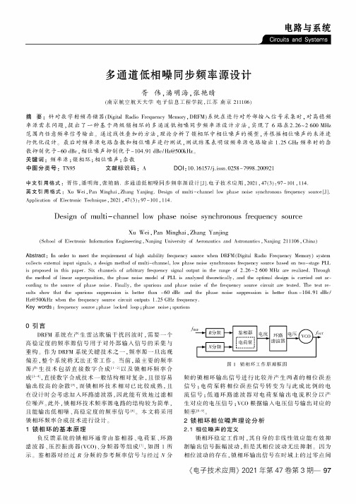
电路与系统多通道低相噪同步频率源设计胥伟,潘明海,张艳睛(南京航空航天大学电子信息工程学院,江苏南京211106)摘要:针对数字射频存储器(Digital Radio Frequency Memory,DRFM)系统在进行对外部输入信号采集时,对高稳频率源需求问题,提出了一种基于两级锁相环的多通道低相噪同步频率源设计方法,实现了6路在2.26〜2600MHz 范围内任意频率信号输出遥通过线性叠加的方法,理论分析了锁相环中相位噪声的模型,并根据相位噪声的来源进行优化设计遥最后对频率源电路杂散和相位噪声进行测试,测试结果表明该频率源电路输出1.25GHz频率时的杂散抑制优于-60dBc,相位噪声抑制优于-104.91dBc/Hz@500kHz遥关键词:频率源;锁相环;相位噪声;杂散中图分类号:TN95文献标识码:A DOI:10.16157/j.issn.0258-7998.200921中文引用格式:胥伟,潘明海,张艳睛.多通道低相噪同步频率源设计[J].电子技术应用,2021,47(3):97-101,114.英文引用格式:Xu Wei,Pan Minghai,Zhang Yanjing.Design of multi-channel low phase noise synchronous frequency source[J]. Application of Electronic Technique,2021,47(3):97-101,114.Design of multi-channel low phase noise synchronous frequency sourceXu Wei,Pan Minghai,Zhang Yanjing(School of Electronic Information Engineering,Nanjing University of Aeronautics and Astronautics,Nanjing211106,China) Abstract:In order to meet the requirement of high stability frequency source when DRFM(Digital Radio Frequency Memory)systemcollects external input signals,a design method of multi-channel,low phase noise synchronous frequency source based on two-stage PLL is proposed in this paper.Six channels of arbitrary frequency signal output in the range of2.26〜2600MHz are realized.Through the method of linear superposition,the phase noise model of PLL is analyzed theoretically,and the optimal design is carried out according to the source of phase noise.Finally,the spurious and phase noise of the frequency source circuit are tested.The test results show that the spurious suppression is better than-60dBc and the phase noise suppression is better than-104.91dBc/ Hz@500kHz when the frequency source circuit outputs 1.25GHz frequency.Key words:frequency source;phase locked loop;phase noise;spurious0引言DRFM系统在产生雷达欺骗干扰回波时,需要一个高稳定度的频率源信号用于对外部输入信号的采集与重构。
25.4x25.4mm插件温控晶振NA-10M-2400系列选型手册
2400 Series-square wave in 25.4x25.4mm DIP packageNA-10M-2400 series oscillators are designed for applications where space is at apremium and good frequency stability is required. The oscillators can be used in many communications applications. A choice of quartz resonators offers a variety of performance versus cost options to fit most applications.ELECTRICAL SPECIFICA TIONS1.OUTPUT (PIN = “R.F. OUTPUT”)ParameterMin. Typ.Max. UnitTest Condition1.1.Frequency10.000000MHz1.2.Initial Accuracy -0.1 +0.1 ppm@ +25 ±1°Cafter turn on power 15 ±1 minutes ≤ 90 days following date code VCO Input at Center Voltage ±0.001V1.3. Waveform Rectangular 1.4.LevelLVTTL “1” level +2.6 +3.3 V “0” level +0.4 V1.5. Load 15 pF1.6. Duty cycle 45 50 55 % @ +1.65V 1.7. Rise/fall time 6 ns 10% to 90% 1.8.Spurious-60dBc2.FREQUENCY STABILITYParameterMin. Typ.Max. UnitTest Condition2.1.Ambient ±3, ±5, ±10 ppb referenced to 25°C Refer to Table 1 : Ordering Information-30 ~ +70 -40 ~ +85°C2.2.Aging-0.5+0.5 ppb per day, at time of shipment Daily -0.5 +0.5 ppb after 30 days Yearly -50 +50 ppb 10 Years-0.3 +0.3 ppm2.3. Voltage -0.5 +0.5 ppb ±5% change 2.4. Short term 0.05 ppb/s root Allan variance 2.5. Load -0.5 +0.5 ppb ±5% change2.6. Warm-up -10 +10 ppb in 10 minutes @ +25 ±1°C referenced to 1 hourRoHS Compliant StandardRev(1)09/2014深圳捷比信--高品质精密元件供应商www.jepsun.comParameter Min. Typ. Max. Unit Test Condition2.7. Phase Noise-95 -90 dBc/Hz @ 1Hz (@25°C)-125 -120 dBc/Hz @ 10Hz (@25°C)-140 -135 dBc/Hz @ 100Hz (@25°C) -148 -145 dBc/Hz @ 1KHz (@25°C) -156 -155 dBc/Hz @ 10KHz (@25°C) -158 -155 dBc/Hz @ 100KHz (@25°C)3. ELECTRICAL FREQUENCY ADJUSTMENT (PIN = “VCO INPUT”)Parameter Min. Typ. Max. Unit Test Condition3.1. Tuning Range-0.5 ppm ***************Referenced to frequency at nominalCenter Voltage+0.5 ppm ***************3.2. Control Voltage 0 +5.0 VOptional, Refer to Table 1 : Ordering Information 0 +4.0 V3.3. Slope Positive3.4. Center Voltage +2.5 VOptional, Refer to Table 1 : Ordering Information Note 1 +2.0 V3.5. Linearity -10 +10 %3.6. Input Impedance 100 kΩ4. INPUT POWER (PIN = “+VDC”)Parameter Min. Typ. Max. Unit Test Condition4.1. Voltage +4.75 +5.0 +5.25 V4.2. Current 800 mA @ turn on4.3. Steady State 1.3 W @ +25°C5. REFERENCE VOLTAGE (PIN = "REFERENCE VOLTAGE")(Optional Function. Refer to Table 1 : Ordering Information.)Parameter Min. Typ. Max. Units Test Condition5.1. Voltage +3.8 +4 +4.2 V Over temperature range in 2.1.5.2. Load 9 kΩ6. ENVIRONMENTALParameter Reference Std. Test Condition6.1. Operating Temperature -40°C to +85°C Note 26.2. Storage Temperature-55°C to +105°C6.3. Humidity MIL-STD-202, Method 103Test Condition A 95% RH @ +40°C,non-condensing,240 hours6.4. Vibration (non-operating) MIL-STD-202, Method 201 0.06” Total p-p, 10 to 55 Hz6.5. Shock (non-operating) MIL-STD-202, Method 213,Test Condition J30g, 11ms, half-sineNote 1. When not connected, VCO INPUT is internally held at this voltage.Note 2. Output maintained over this temperature range. Other requirements of this specification may not be met when operating outside the temperature range in 2.1.Rev(1)09/2014深圳捷比信--高品质精密元件供应商www.jepsun.comOUTLINE DRA WINGTable 1 : ORDERING INFORMA TIONRev(1)09/2014 深圳捷比信--高品质精密元件供应商www.jepsun.com。
OPA380资料
proper handling and installation procedures can cause damage. ESD damage can range from subtle performance degradation to complete device failure. Precision integrated circuits may be more susceptible to damage because very small parametric changes couldPACKAGING INFORMATIONOrderable Device Status (1)Package Type Package Drawing Pins Package Qty Eco Plan (2)Lead/Ball Finish MSL Peak Temp (3)OPA2380AIDGKR ACTIVE MSOP DGK 82500Green (RoHS &no Sb/Br)CU NIPDAU Level-2-260C-1YEAR OPA2380AIDGKT ACTIVE MSOP DGK 8250Green (RoHS &no Sb/Br)CU NIPDAU Level-2-260C-1YEAR OPA380AID ACTIVE SOIC D 8100None CU SNPB Level-1-220C-UNLIM OPA380AIDGKR ACTIVE MSOP DGK 82500None CU NIPDAU Level-1-220C-UNLIM OPA380AIDGKT ACTIVE MSOP DGK 8250None CU NIPDAU Level-1-220C-UNLIM OPA380AIDRACTIVESOICD82500NoneCU SNPBLevel-1-220C-UNLIM(1)The marketing status values are defined as follows:ACTIVE:Product device recommended for new designs.LIFEBUY:TI has announced that the device will be discontinued,and a lifetime-buy period is in effect.NRND:Not recommended for new designs.Device is in production to support existing customers,but TI does not recommend using this part in a new design.PREVIEW:Device has been announced but is not in production.Samples may or may not be available.OBSOLETE:TI has discontinued the production of the device.(2)Eco Plan -May not be currently available -please check /productcontent for the latest availability information and additional product content details.None:Not yet available Lead (Pb-Free).Pb-Free (RoHS):TI's terms "Lead-Free"or "Pb-Free"mean semiconductor products that are compatible with the current RoHS requirements for all 6substances,including the requirement that lead not exceed 0.1%by weight in homogeneous materials.Where designed to be soldered at high temperatures,TI Pb-Free products are suitable for use in specified lead-free processes.Green (RoHS &no Sb/Br):TI defines "Green"to mean "Pb-Free"and in addition,uses package materials that do not contain halogens,including bromine (Br)or antimony (Sb)above 0.1%of total product weight.(3)MSL,Peak Temp.--The Moisture Sensitivity Level rating according to the JEDECindustry standardclassifications,and peak solder temperature.Important Information and Disclaimer:The information provided on this page represents TI's knowledge and belief as of the date that it is provided.TI bases its knowledge and belief on information provided by third parties,and makes no representation or warranty as to the accuracy of such information.Efforts are underway to better integrate information from third parties.TI has taken and continues to take reasonable steps to provide representative and accurate information but may not have conducted destructive testing or chemical analysis on incoming materials and chemicals.TI and TI suppliers consider certain information to be proprietary,and thus CAS numbers and other limited information may not be available for release.In no event shall TI's liability arising out of such information exceed the total purchase price of the TI part(s)at issue in this document sold by TI to Customer on an annual basis.PACKAGE OPTION ADDENDUM9-Dec-2004Addendum-Page 1IMPORTANT NOTICETexas Instruments Incorporated and its subsidiaries (TI) reserve the right to make corrections, modifications, enhancements, improvements, and other changes to its products and services at any time and to discontinue any product or service without notice. Customers should obtain the latest relevant information before placing orders and should verify that such information is current and complete. All products are sold subject to TI’s terms and conditions of sale supplied at the time of order acknowledgment.TI warrants performance of its hardware products to the specifications applicable at the time of sale in accordance with TI’s standard warranty. T esting and other quality control techniques are used to the extent TI deems necessary to support this warranty. Except where mandated by government requirements, testing of all parameters of each product is not necessarily performed.TI assumes no liability for applications assistance or customer product design. Customers are responsible for their products and applications using TI components. T o minimize the risks associated with customer products and applications, customers should provide adequate design and operating safeguards.TI does not warrant or represent that any license, either express or implied, is granted under any TI patent right, copyright, mask work right, or other TI intellectual property right relating to any combination, machine, or process in which TI products or services are used. Information published by TI regarding third-party products or services does not constitute a license from TI to use such products or services or a warranty or endorsement thereof. Use of such information may require a license from a third party under the patents or other intellectual property of the third party, or a license from TI under the patents or other intellectual property of TI.Reproduction of information in TI data books or data sheets is permissible only if reproduction is without alteration and is accompanied by all associated warranties, conditions, limitations, and notices. Reproduction of this information with alteration is an unfair and deceptive business practice. TI is not responsible or liable for such altered documentation.Resale of TI products or services with statements different from or beyond the parameters stated by TI for that product or service voids all express and any implied warranties for the associated TI product or service and is an unfair and deceptive business practice. TI is not responsible or liable for any such statements. Following are URLs where you can obtain information on other Texas Instruments products and application solutions:Products ApplicationsAmplifiers Audio /audioData Converters Automotive /automotiveDSP Broadband /broadbandInterface Digital Control /digitalcontrolLogic Military /militaryPower Mgmt Optical Networking /opticalnetwork Microcontrollers Security /securityTelephony /telephonyVideo & Imaging /videoWireless /wirelessMailing Address:Texas InstrumentsPost Office Box 655303 Dallas, Texas 75265Copyright 2004, Texas Instruments Incorporated。
铷钟FS725c_Frequency Standards

Frequency StandardsFS725 — Benchtop rubidium frequency standard· 10 MHz and 5 MHz outputs · 1 pps input and output for GPS synchronization· 20 year aging less than 0.005 ppm · Ultra-low phase noise (<−130 dBc/Hz at 10 Hz) · Built-in distribution amplifiers (up to 22 outputs) · RS-232 computer interface · Two status alarm relays· FS725 ... $2695 (U.S. list)The FS725 integrates a rubidium oscillator (SRS model PRS10), a low-noise AC power supply, and distribution amplifiers in a compact, half-width 2U chassis. It provides stable and reliable performance with an estimated 20 year aging of less than 5 × 10⁻⁹, and a demonstrated rubidium oscillator MTBF of over 200,000 hours. The FS725 is an ideal instrument for calibration and R&D laboratories, or any application requiring a precision frequency standard. There are two 10 MHz and one 5 MHz outputs with exceptionally low phase noise (–130 dBc/Hz at 10 Hz offset) and one second Allan variance (<2 × 10–11). The FS725 can be phase-locked to an external 1 pps reference (like GPS) providing Stratum 1 performance. A 1 pps output is also provided that has less than 1 ns of jitter, and may be set with 1 ns resolution.Up to three internal distribution modules can be added to the FS725. Each module has four 10 MHz outputs, one 5 MHz output, and one 1 pps output, all with the same low phase noise, harmonic distortion and jitter.An RS-232 interface allows direct communication with the rubidium oscillator. Using the provided Windows software, you can easily monitor and control 1 pps timing, and determine the instrument’s operational status.There are two alarm relays that indicate the status of the rubidium oscillator lock state and synchronization to an external 1 pps input. The relays are SPDT, providing both normally-open and normally-closed contacts.FS725 Specificationsexternal 1 pps input is applied, lockis maintained between the 1 pps input and 1 pps output, withcomputer adjustable time constantfrom 8 minutes to 18 hours. 10 MHz outputs Two 50 Ω isolated sine outputs 5 MHz output One 50 Ω sine output 1 pps output One 50 Ω pulse outputOptional outputs Each option board provides four 10 MHz, one 5 MHz, and one 1 pps outputs. Up to 3 boards can be installed.Alarm relays Max. current, 3 A. SPDT, normally open or normally closed. May be wired in parallel with other relays to “wire-or” a single alarm.Rb lock Relay status matches the front-panel “Locked” LED.1 pps Relay status matches the front-panel “1 pps sync” LED.RS-232 9-pin connector configured as DCE, 9600 baud. Windows RbMon software is provided.EnvironmentalOperating temperature +10 °C to +40 °CTemperature stability ∆f/f < ±1 × 10⁻¹⁰ (+10 °C to +40 °C)Storage temperature –55 °C to +85 °CMagnetic field ∆f/f < 2 × 10⁻¹⁰ (1 Gauss field reversal)Relative humidity 95 % (non-condensing)GeneralAC power 90 to 132 VAC or 175 to 264 VAC,47 to 63 Hz, 50 WDimensions, weight 8.5" × 3.5" × 13" (WHL), 9 lbs.Warranty One year parts and labor on defectsin materials and workmanshipFS725 rear panel (with Opt. 03)Ordering InformationFS725 Benchtop Rb frequency standard $2695Option 01 Distribution amplifier (6 outputs) $400Option 02 Distribution amplifier (12 outputs) $800 Option 03 Distribution amplifier (18 outputs) $1200 O725RMD Double rack mount kit $100O725RMSSingle rack mount kit $100。
A general theory of phase noise in electrical oscillators
A General Theory of Phase Noisein Electrical OscillatorsAli Hajimiri,Student Member,IEEE,and Thomas H.Lee,Member,IEEE Abstract—A general model is introduced which is capableof making accurate,quantitative predictions about the phasenoise of different types of electrical oscillators by acknowledgingthe true periodically time-varying nature of all oscillators.Thisnew approach also elucidates several previously unknown designcriteria for reducing close-in phase noise by identifying the mech-anisms by which intrinsic device noise and external noise sourcescontribute to the total phase noise.In particular,it explains thedetails of how1=f noise in a device upconverts into close-inphase noise and identifies methods to suppress this upconversion.The theory also naturally accommodates cyclostationary noisesources,leading to additional important design insights.Themodel reduces to previously available phase noise models asspecial cases.Excellent agreement among theory,simulations,andmeasurements is observed.Index Terms—Jitter,oscillator noise,oscillators,oscillator sta-bility,phase jitter,phase locked loops,phase noise,voltagecontrolled oscillators.I.I NTRODUCTIONT HE recent exponential growth in wireless communicationhas increased the demand for more available channels inmobile communication applications.In turn,this demand hasimposed more stringent requirements on the phase noise oflocal oscillators.Even in the digital world,phase noise in theguise of jitter is important.Clock jitter directly affects timingmargins and hence limits system performance.Phase and frequencyfluctuations have therefore been thesubject of numerous studies[1]–[9].Although many modelshave been developed for different types of oscillators,eachof these models makes restrictive assumptions applicable onlyto a limited class of oscillators.Most of these models arebased on a linear time invariant(LTI)system assumptionand suffer from not considering the complete mechanism bywhich electrical noise sources,such as device noise,becomephase noise.In particular,they take an empirical approach indescribing the upconversion of low frequency noise sources,suchascorner in the phase noise spectrum is smallerthanis the amplitude,0018–9200/98$10.00©1998IEEEFig.1.Typical plot of the phase noise of an oscillator versus offset fromcarrier.is an arbitrary,fixed phase refer-ence.Therefore,the spectrum of an ideal oscillator with norandom fluctuations is a pair of impulsesat.In a practical oscillator,however,the output is more generally givenbyandis aperiodic function with period2andrepresents the single side-band power at a frequency offsetofandis dominated by its phaseportion,,known as phase noise,which we will simplydenoteas.Fig.2.A typical RLC oscillator.The semi-empirical model proposed in [1]–[3],known also as the Leeson–Cutler phase noise model,is based on an LTI assumption for tuned tank oscillators.It predicts the followingbehaviorfor:is an empirical parameter (often called the “deviceexcess noisenumber”),is the absolutetemperature,),andregion can beobtained by applying a transfer function approach as follows.The impedance of a parallel RLC,for,is easily calculated tobeHAJIMIRI AND LEE:GENERAL THEORY OF PHASE NOISE IN ELECTRICAL OSCILLATORS181Fig.3.Phase and amplitude impulse response model.a multiplicativefactor,a priori.One importantreason is that much of the noise in a practical oscillatorarises from periodically varying processes and is thereforecyclostationary.Hence,as mentioned in[3],region of the spectrum can be calculatedasregion is thus easily obtained,the expressionforthecorner of thephase noise is the same asthe(7)whereis the effective series resistance,givenbyare shown in Fig.2.Note that itis still not clear how tocalculateinputs(each associated with one noise source)and two outputsthat are the instantaneous amplitude and excess phase of theoscillator,,as defined by(1).Noise inputs to thissystem are in the form of current sources injecting into circuitnodes and voltage sources in series with circuit branches.Foreach input source,both systems can be viewed as single-input,single-output systems.The time and frequency-domainfluctuationsof can be studied by characterizingthe behavior of two equivalent systems shown in Fig.3.Note that both systems shown in Fig.3are time variant.Consider the specific example of an ideal parallel LC oscillatorshown in Fig.4.If we inject a current impulse as shown,the amplitude and phase of the oscillator will have responsessimilar to that shown in Fig.4(a)and(b).The instantaneousvoltagechange182IEEE JOURNAL OF SOLID-STATE CIRCUITS,VOL.33,NO.2,FEBRUARY1998(a)(b)Fig.5.(a)A typical Colpitts oscillator and (b)a five-stage minimum size ring oscillator.capacitor and will not affect the current through the inductor.It can be seen from Fig.4that the resultant changeinis time dependent.In particular,if the impulse is applied at the peak of the voltage across the capacitor,there will be no phase shift and only an amplitude change will result,as shown in Fig.4(a).On the other hand,if this impulse is applied at the zero crossing,it has the maximum effect on the excessphase,which results in no phase change and changes only the amplitude,while applying an impulse atpointm CMOS inverter chain ring oscillatorshown in Fig.5(b).The results are shown in Fig.6(a)and (b),respectively.The impulse is applied close to a zerocrossing,(a)(b)Fig.6.Phase shift versus injected charge for oscillators of Fig.5(a)and (b).where it has the maximum effect on phase.As can be seen,the current-phase relation is linear for values of charge up to 10%of the total charge on the effective capacitance of the node of interest.Also note that the effective injected charges due to actual noise and interference sources in practical circuits are several orders of magnitude smaller than the amounts of charge injected in Fig.6.Thus,the assumption of linearity is well satisfied in all practical oscillators.It is critical to note that the current-to-phase transfer func-tion is practically linear even though the active elements may have strongly nonlinear voltage-current behavior.However,the nonlinearity of the circuit elements defines the shape of the limit cycle and has an important influence on phase noise that will be accounted for shortly.We have thus far demonstrated linearity,with the amount of excess phase proportional to the ratio of the injected charge to the maximum charge swing across the capacitor on the node,i.e.,when the impulseis injected.Therefore,the unit impulse response for excess phase can be expressedas(10)whereis the unit step.Wecallwhich describes how much phase shift results fromapplying a unit impulse attimeis a function of the waveformor,equivalently,the shape of the limit cycle which,in turn,is governed by the nonlinearity and the topology of the oscillator.Given the ISF,the output excessphaseHAJIMIRI AND LEE:GENERAL THEORY OF PHASE NOISE IN ELECTRICAL OSCILLATORS183(a)(b)Fig.7.Waveforms and ISF’s for(a)a typical LC oscillator and(b)a typical ring oscillator.where represents the input noise current injected into the node of interest.Since the ISF is periodic,it can be expanded in a Fourierseriesth harmonic.As will be seenlater,for an arbitrary inputcurrent injected into any circuit node,once the variousFourier coefficients of the ISF have been found.As an illustrative special case,suppose that we inject a lowfrequency sinusoidal perturbation current into the node ofinterest at a frequencyof(14)where.The argumentsof all the integrals in(13)are at frequencies higherthanand are significantly attenuated by the averaging nature ofthe integration,except the term arising from thefirst integral,whichinvolves.Therefore,the only significant termin,denotedas.As an important second special case,consider a current at afrequency close to the carrier injected into the node of interest,givenby.A process similar to thatof the previous case occurs except that the spectrumofFig.8.Conversion of the noise around integer multiples of the oscillationfrequency into phase noise.consists of two impulsesat as shown in Fig.8.This time the only integral in(13)which will have a lowfrequency argument isfor is givenby.More generally,(13)suggests that applying acurrentclose to any integer multiple of theoscillation frequency will result in two equal sidebandsat.Hence,in the generalcaseusing(13).Computing the power spectral density(PSD)of the oscillatoroutputvoltage requires knowledge of how the outputvoltage relates to the excess phase variations.As shown inFig.8,the conversion of device noise current to output voltagemay be treated as the result of a cascade of two processes.Thefirst corresponds to a linear time variant(LTV)current-to-phase converter discussed above,while the second is anonlinear system that represents a phase modulation(PM),which transforms phase to voltage.To obtain the sidebandpower around the fundamental frequency,the fundamentalharmonic of the oscillatoroutputas the input.Substitutinggiven by(17).Therefore,an injected currentat(18)184IEEE JOURNAL OF SOLID-STATE CIRCUITS,VOL.33,NO.2,FEBRUARY1998(a)(b)Fig.9.Simulated power spectrum of the output with current injection at(a) f m=50MHz and(b)f0+f m=1:06GHz.This process is shown in Fig.8.Appearance of the frequencydeviation.This type of nonlinearity does not directlyappear in the phase transfer characteristic and shows itself onlyindirectly in the ISF.It is instructive to compare the predictions of(18)withsimulation results.A sinusoidal current of10MHz.This power spectrum is obtained usingthe fast Fourier transform(FFT)analysis in HSPICE96.1.Itis noteworthy that in this version of HSPICE the simulationartifacts observed in[9]have been properly eliminated bycalculation of the values used in the analysis at the exactpoints of interest.Note that the injected noise is upconvertedinto two equal sidebandsat,where is the average capacitance on each node of thecircuitand is the maximum swing across it.For thisoscillator,–whose power spectral density has both aflat region anda,which in turn becomeclose-in phase noise in the spectrumof,as illustrated inFig.11.It can be seen that thetotal is given by the sumof phase noise contributions from device noise in the vicinityof the integer multiplesof,weighted by thecoefficients.This is shown in Fig.12(a)(logarithmic frequency scale).The resulting single sideband spectral noisedensity isplotted on a logarithmic scale in Fig.12(b).The sidebands inthe spectrumof,in turn,result in phase noise sidebandsin the spectrumof through the PM mechanism discussin the previous subsection.This process is shown in Figs.11and12.The theory predicts the existenceof,andflatregions for the phase noise spectrum.The low-frequency noisesources,such asflicker noise,are weighted by thecoefficientand showaHAJIMIRI AND LEE:GENERAL THEORY OF PHASE NOISE IN ELECTRICAL OSCILLATORS185Fig.11.Conversion of noise to phase fluctuations and phase-noise side-bands.the white noise terms are weighted byother coefficients and give rise tothecontainsregions.Finally,the flat noise floor in Fig.12(b)arises from the white noise floor of the noise sources in the oscillator.The total sideband noise power is the sum of these two as shown by the bold line in the same figure.To carry out a quantitative analysis of the phase noise sideband power,now consider an input noise current with a white power spectraldensityHz.Based on the foregoing development and (18),the total single sideband phase noise spectral density in dB below the carrier per unit bandwidth due to the source on one node at an offset frequencyof(20)where.As aresultregion of the phase noise spectrum.For a voltage noise source in series with aninductor,,wherecorner of thephase noise.It is important to note that it is by nomeans(a)(b)Fig.12.(a)PSD of (t )and (b)single sideband phase noise power spectrum,L f 1!g .obvious from the foregoing development thatthecanbe describedby(22)whereportion of the phasenoisespectrum:corner,corner in the phase noisespectrum:phase noise corner due to internal noisesources is not equal tothe186IEEE JOURNAL OF SOLID-STATE CIRCUITS,VOL.33,NO.2,FEBRUARY1998Fig.13.Collector voltage and collector current of the Colpitts oscillator of Fig.5(a).D.Cyclostationary Noise SourcesIn addition to the periodically time-varying nature of the system itself,another complication is that the statistical prop-erties of some of the random noise sources in the oscillator may change with time in a periodic manner.These sources are referred to as cyclostationary.For instance,the channel noise of a MOS device in an oscillator is cyclostationary because the noise power is modulated by the gate source overdrive which varies with time periodically.There are other noise sources in the circuit whose statistical properties do not depend on time and the operation point of the circuit,and are therefore called stationary.Thermal noise of a resistor is an example of a stationary noise source.A white cyclostationary noise current can be decom-posed as[13]:is a white cyclostationaryprocess,is awhite stationary processandis a deterministic periodic function describing the noise amplitude modulation.Wedefineto be a normalized function with a maximum value of1.Thisway,is equal to the maximum mean square noisepower,,which changes periodically with time.Applying the above expression forto(11),(27)wherecan be derived easily from device noise character-istics and operating point.Hence,this effective ISF shouldbeFig.14.0(x ),0e (x ),and (x )for the Colpitts oscillator of Fig.5(a).used in all subsequent calculations,in particular,calculation of thecoefficients .Note that there is a strong correlation between the cyclosta-tionary noise source and the waveform of the oscillator.The maximum of the noise power always appears at a certain point of the oscillatory waveform,thus the average of the noise may not be a good representation of the noise power.Consider as one example the Colpitts oscillator of Fig.5(a).The collector voltage and the collector current of the transistor are shown in Fig.13.Note that the collector current consists of a short period of large current followed by a quiet interval.The surge of current occurs at the minimum of the voltageacross the tank where the ISF is small.Functions,andfor this oscillator are shown in Fig.14.Note that,in thiscase,is quite differentfrom is at a maximum,i.e.,thesensitivity is large)at the same time the noise power is large.Functions,and for the ring oscillator of Fig.5(b)are shown in Fig.15.Note that in the case of theringoscillatorare almost identical.This indicates that the cyclostationary properties of the noise are less important in the treatment of the phase noise of ring oscillators.This unfortunate coincidence is one of the reasons why ring oscillators in general have inferior phase noise performance compared to a Colpitts LC oscillator.The other important reason is that ring oscillators dissipate all the stored energy during one cycle.E.Predicting Output Phase Noise with Multiple Noise Sources The method of analysis outlined so far has been used to predict how much phase noise is contributed by a single noise source.However,this method may be extended to multiple noise sources and multiple nodes,as individual contributions by the various noise sources may be combined by exploiting superposition.Superposition holds because the first system of Fig.8is linear.HAJIMIRI AND LEE:GENERAL THEORY OF PHASE NOISE IN ELECTRICAL OSCILLATORS187Fig.15.0(x ),0e (x ),and (x )for the ring oscillator of Fig.5(b).The actual method of combining the individual contributions requires attention to any possible correlations that may exist among the noise sources.The complete method for doing so may be appreciated by noting that an oscillator has a current noise source in parallel with each capacitor and a voltage noise source in series with each inductor.The phase noise in the output of such an oscillator is calculated using the following method.1)Find the equivalent current noise source in parallel with each capacitor and an equivalent voltage source in series with each inductor,keeping track of correlated and noncorrelated portions of the noise sources for use in later steps.2)Find the transfer characteristic from each source to the output excess phase.This can be done as follows.a)Find the ISF for each source,using any of the methods proposed in the Appendix,depending on the required accuracy and simplicity.b)Find,the amount of charge swing across the effec-tive capacitor it is injectingintois the tank capacitor,andis the maximum voltage swing across the tank.Equation (19)reducesto,the result obtained in [8]istwo times larger than the result of (29).Assuming that the total noise contribution in a parallel tank oscillator can be modeled using an excess noisefactorandfor valuesofregionare suggested by (24),which shows thatthe188IEEE JOURNAL OF SOLID-STATE CIRCUITS,VOL.33,NO.2,FEBRUARY1998(a)(b)(c)(d)Fig.16.(a)Waveform and (b)ISF for the asymmetrical node.(c)Waveform and (d)ISF for one of the symmetrical nodes.waveform.One such property concerns the rise and fall times;the ISF will have a large dc value if the rise and fall times of the waveform are significantly different.A limited case of this for odd-symmetric waveforms has been observed [14].Although odd-symmetric waveforms havesmall coefficients,the class of waveforms withsmall is not limited to odd-symmetric waveforms.To illustrate the effect of a rise and fall time asymmetry,consider a purposeful imbalance of pull-up and pull-down rates in one of the inverters in the ring oscillator of Fig.5(b).This is obtained by halving the channelwidthAatMHz is applied to one of the symmetric nodes ofthe(a)(b)Fig.17.Simulated power spectrum with current injection at f m =50MHz for (a)asymmetrical node and (b)symmetrical node.oscillator.In the second experiment,the same source is applied to the asymmetric node.As can be seen from the power spectra of the figure,noise injected into the asymmetric node results in sidebands that are 12dB larger than at the symmetric node.Note that (30)suggests that upconversion of low frequency noise can be significantly reduced,perhaps even eliminated,byminimizing ,at least in principle.Sincedepends on the waveform,this observation implies that a proper choice of waveform may yield significant improvements in close-in phase noise.The following experiment explores this concept by changing the ratioofA of sinusoidal current at 100MHz intoone node.The sideband power below carrier as a function oftheA at 50MHz injected at the drain node of one of the buffer stages results in two equal sidebands,Fig.18.Simulated and predicted sideband power for low frequency injection versus PMOS to NMOS W=Lratio.Fig.19.Four-stage differential ring oscillator.upconversion of noise to close-in phase noise,even though differential signaling is used.Since the asymmetry is due to the voltage dependent con-ductance of the load,reduction of the upconversion might be achieved through the use of a perfectly linear resistive load,because the rising and falling behavior is governed by an RC time constant and makes the individual waveforms more symmetrical.It was first observed in the context of supply noise rejection [15],[16]that using more linear loads can reduce the effect of supply noise on timing jitter.Our treatment shows that it also improves low-frequency noise upconversion into phase noise.Another symmetry-related property is duty cycle.Since the ISF is waveform-dependent,the duty cycle of a waveform is linked to the duty cycle of the ISF.Non-50%duty cyclesgenerally result inlargerforeven tank of an LC oscillator is helpful in this context,since ahighMHz,MHz,and MHz,and the sideband powersatis proportionalto,and hence the sideband power is proportionaltoA (rms)at20dB/decade,again in complete accordance with (18).The third experiment aims at verifying the effect of thecoefficientson the sideband power.One of the predictions of the theory isthatis responsible for the upconver-sion of low frequency noise.As mentionedbefore,is a strong function of waveform symmetry at the node into which the current is injected.Noise injected into a node with an asymmetric waveform (created by making one inverter asymmetric in a ring oscillator)would result in a greater increase in sideband power than injection into nodes with more symmetric waveforms.Fig.22shows the results of an experiment performed on a five-stage ring oscillator in which one of the stages is modified to have an extra pulldownFig.21.Measured sideband power versus f m ,for injections in vicinity of multiples of f 0.Fig.22.Power of the sidebands caused by low frequency injection into symmetric and asymmetric nodes of the ring oscillator.NMOS device.A current of20m,5-V CMOS process runningatandregion.For thisprocess we have a gate oxide thicknessofnm and threshold voltagesofVand mandm m,and a lateral diffusionof fF.Therefore,Fig.23.Phase noise measurements for a five-stage single-ended CMOS ring oscillator.f 0=232MHz,2- m processtechnology.identical noise sources thenpredictskHz,this equationpredictskHz dBc/Hz,in good agreement with a measurementofregion,it is enough to calculatetheratio iscalculated to be 0.3,which predictsamandmm,whichresults in a total capacitance of 43.5fFand,or122.5d B c /H z ,a g a i n i na g r e e m e n t w i t h p r e d i c t i o n s .T h e r a t i o i s c a l c u l a t e t ob e 0.17w h ic h p r ed i c t sar e g i o n b e h a v i o r .I t i n v o l v e s a s e v es t a r v e d ,s i n g l e -e n d e d r i n g o s c i l l a t o r i s t a g e c o n s i s t s o f a n a d d i t i o n a l N M O S a i n s e r i e s .T h e g a t e d r i v e s o f t h e a d d e d i n d e p e n d e n t c o n t r o l o f t h e r i s e a n d f a l l t h e p h a s e n o i s e w h e n t h e c o n t r o l v o l t a g a c h i e v e s y m m e t r y v e r s u s w h e n t h e y a r e n c o n t r o l v o l t a g e s a r e a d j u s t e d t o k e e p t h eFig.24.Phase noise measurements for an 11-stage single-ended CMOS ring oscillator.f 0=115MHz,2- m processtechnology.Fig.25.Effect of symmetry in a seven-stage current-starved single-ended CMOS VCO.f 0=60MHz,2- m process technology.constant at 60MHz.As can be seen,making the waveform more symmetric has a large effect on the phase noise intheregion.Another experiment on the same circuit is shown in Fig.26,which shows the phase noise power spectrum at a 10kHz offset versus the symmetry-controlling voltage.For all the data points,the control voltages are adjusted to keep the oscillation frequency at 50MHz.As can be seen,the phase noise reaches a minimum by adjusting the symmetry properties of the waveform.This reduction is limited by the phase noiseinm CMOS process.Each stage istapped with an equal-sized buffer.The tail current source has a quiescent current of108fFand the voltage swingisV,which resultsin fF.The total channel noise current on eachnodeFig.26.Sideband power versus the voltage controlling the symmetry of the waveform.Seven-stage current-starved single-ended CMOS VCO.f 0=50MHz,2- m processtechnology.Fig.27.Phase noise measurements for a four-stage differential CMOS ring oscillator.f 0=200MHz,0.5- m process technology.is,the phase noise inthe,or103.9d B c /H z ,a g a i n i n a g r e e m e n t w i tA l s o n o t e t h a t d e s p i t e d i f f e r e n t i a l s y m m e trw h i l e k e e p i n g t h e e f f e c t i v ec a p a c i t a n ce c o n s t a n t t o m a i n t a iand e c r e a s e s t h e c o n d u c t i o n a n g l e ,a n d t h e r e f f e c t i ve.T h e p h a s e n o i s e u l t i m a t e l y i n c r e a s e s(h e r e ,a b o u t0.2)t h a t m i n i m i z e s t h e p h a s e n o i s e .T h i s r t h e o r e t i c a l b a s i s f o r t h e c o m m o n r u l e -o f -t hFig.28.Sideband power versus capacitive division ratio.Bipolar LC Colpitts oscillator f 0=100MHz.use)inColpitts oscillators [17].VI.C ONCLUSIONThis paper has presented a model for phase noise which explains quantitatively the mechanism by which noise sources of all types convert to phase noise.The power of the model derives from its explicit recognition of practical oscillators as time-varying systems.Characterizing an oscillator with the ISF allows a complete description of the noise sensitivity of an oscillator and also allows a natural accommodation of cyclostationary noise sources.This approach shows that noise located near integer mul-tiples of the oscillation frequency contributes to the total phase noise.The model specifies the contribution of those noise components in terms of waveform properties and circuit parameters,and therefore provides important design insight by identifying and quantifying the major sources of phase noise degradation.In particular,it shows that symmetry properties of the oscillator waveform have a significant effect on the upconversion of low frequency noise and,hence,thefromit.The second method is based on an analytical state-space approach to find the excess phase change caused by an impulse of current from the oscillation waveforms.The third method is an easy-to-use approximate method.A.Direct Measurement of Impulse ResponseIn this method,an impulse is injected at different relative phases of the oscillation waveform and the oscillatorsimulatedFig.29.State-space trajectory of an n th-order oscillator.for a few cycles afterwards.By sweeping the impulse injec-tion time across one cycle of the waveform and measuring the resulting timeshiftis the period of oscillation.Fortunately,many implementations of SPICE have an internal feature to perform the sweep automatically.Since for each impulse one needs to simulate the oscillator for only a few cycles,the simulation executes rapidly.Onceth-order system can be represented by its trajectory inanwhich suddenly changes the state of the systemto.As discussed earlier,amplitude variations eventually die away,but phase variations do not.Application of the perturbation impulse causes a certain change in phase in either a negative or positive direction,depending on the state-vector and the direction of the perturbation.To calculate the equivalent time shift,we first find the projection of the perturbation vector on a unity vector in the direction of motion,i.e.,the normalized velocityvectoris the equivalent displacement along the trajectory,and,which arises from the projection operation.Theequivalent time shift is given by the displacement divided by。
低相噪_高集成度频率源的研制_周文衎
·1259·低相噪、高集成度频率源的研制周文衎 童 超 王晓江(南京电子设备研究所,南京 210007)zhouwenkan1314@摘 要:本文介绍了一种低杂散、低相噪、高集成度的频率源的研制。
该频率源采用Hittite 公司的鉴相器HMC830LP6G ,通过锁相产生1GHz 信号,杂散抑制≥70dBc 、相噪达到-116dBc/Hz@1kHz 。
由于鉴相器内部集成VCO ,所有器件布局在50×20mm 的范围内,大大减少了电路板的面积,提高了设计的集成度,实现了小型化。
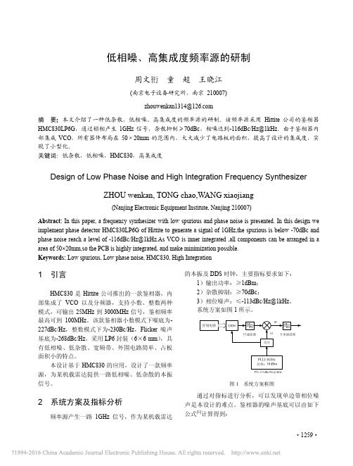
关键词:低杂散,低相噪,HMC830,高集成度Design of Low Phase Noise and High Integration Frequency SynthesizerZHOU wenkan, TONG chao,WANG xiaojiang(Nanjing Electronic Equipment Institute, Nanjing 210007)Abstract: In this paper, a frequency synthesizer with low spurious and phase noise is presented. In this design we implement phase detector HMC830LP6G of Hittite to generate a signal of 1GHz,the spurious is below -70dBc and phase noise reach a level of -116dBc/Hz@1kHz.As VCO is inner integrated ,all components can be arranged in a area of 50×20mm,so the PCB is highly integrated, and make minimization possible. Keywords: Low spurious, Low phase noise, HMC830, High Integration1 引言HMC830是Hittite 公司推出的一款鉴相器,内部集成了VCO 以及分频器,支持小数、整数两种模式,可输出25MHz 到3000MHz 信号,鉴相频率最高可到100MHz 。
RF-CMOSOscillatorswithswitchedTuning

Fully integrated CMOS oscillators are of great interest for use in single-chip wireless transceivers.In most oscillator circuits reported to date that operate in the 0.9 to 2 GHz frequency range, an integrated spiral inductor sets the frequency . It is generally believed that an LC oscillator, even when it uses a low-Q inductor, displays a lower phase noise than a ring oscillator. However , due to the absence of a good varactor compatible with CMOS technology,the integrated LC oscillator suffers from a very limited tuning range . Although this tuning range may encompass the limited frequency agility re-quired in an RF oscillator, for instance to span the modulation bandwidth in a transmitter, it will seldom cover the much larger lot-to-lot process variations manifest as spreads of up to 20% in capacitance.Fortunately, the self-inductance of a metal spiral does not suffer spreads, because it depends on a precise number of turns and on the geometry of metal traces which is little affected by fluctuations in lithography.This work addresses the practical problem of how to design RF CMOS oscillators with a wide enough tuning range to reliably cover processvariations, without compromising current drain or phase noise. Prototypes were developed in the 0.6-µm MOSIS CMOS process to oscillate at up to 1.8 GHz with a sub-3V supply. The tuning method exploits digital capabilities and MOS analog switches.On-Chip Components for T uningCapacitorsA CMOS oscillator may be continuously tuned with two possible voltage-dependent capacitors: thevoltage-dependent junction capacitor at the source or drain diffusion; or the voltage-dependent MOS capacitor (a MOSFET with source and drainshorted). Now in a MOS oscillator the capacitor in the resonant circuit is subject to large signal swings,on the order of the supply voltage. Thus, depending on its amplitude, the oscillation probes differentregions of the MOS capacitor’s small-signal C-V characteristic, from inversion, through depletion,into accumulation (Figure 1). The average capaci-tance it experiences varies with the bias V GS –V t . The frequency of oscillation depends on the averagecapacitance, while the effect of the varying incremen-tal capacitance across a cycle is to distort the oscillat-ing waveform into a non-sinusoid. This distortion is usually small, and in any case unimportant in this application.MOS capacitor tuning is used here, as opposed to junction capacitor tuning we have described in previous work [1]. The control voltage on the MOS capacitor may be swept across the full power supply with no fear of forward bias. Also, in a junctioncapacitor the spreading resistance in the substrate or well is set by junction size and doping, whereas in a MOS capacitor it depends on the region of operation at any instant of time. In accumulation, it is a spreading resistance in the substrate to ground; in depletion, it is this spreading resistance in series with a small capacitor; and in inversion, it is the resistance of the MOSFET channel, which is much lower than the spreading resistance, even at a modest V GS –V t .The oscillator current drain is lowered by using as large a load impedance as is possible at theoscillation frequency. Assuming the inductor domi-nates the quality factor, Q , of this LC tuned circuit load, this is tantamount to tuning the oscillator with the largest possible inductor . However, as the induc-tance of a metal spiral is made larger, its self-capacitance increases as well, eventually causing the inductor to self-resonate below the target oscillation frequency, here 1.8 GHz. Therefore, spiral structures with the lowest self-capacitance per unit inductance were investigated.Multi-layer InductorsThe three levels of metal available in this process make it possible to fabricate a useful multi-layer spiral inductor [2, 3], whose inductance per unit area, owing to solenoid-like properties, rises almost quadratically with the number of layers. Although there is substantial capacitance between the turns inRF-CMOS Oscillators with Switched T uningA. Kral, F . Behbahani, and A. A. AbidiElectrical Engineering DepartmentUniversity of California Los Angeles, CA 90095-1594Research supported by DARP A, Rockwell International,Harris Semiconductor, Motorola, Ericsson, Toshiba, and the State of California MICRO Program.This paper was presented at the Custom IC Conference , Santa Clara, CA, May 1998.It appears on pages 555-558 of the proceedings.the closest layers of such a spiral (Figure 3), the capacitance to substrate experiences the largest signal voltage. Without resorting to selective removal of the substrate underlying the inductor [4], three-layer inductors of about 10 nH may be realized for use at 2 GHz.This inductor suffers mainly from the loss due to the resistance of the metal windings, but also due to substrate losses caused by displacement currents flowing in the substrate spreading resistance, and due to eddy currents induced in the heavily doped substrate under the 6-µm thick epi layer. A laminated grounded polysilicon shield plate is placed under all the inductors to prevent the displacement currents from flowing into the substrate [5]. A simple four-element model (Figure 2) is found to accurately fit the complex impedance of standalone test inductors measured with a PicoProbe® across 0.8 to 5 GHz. The quality factor, Q, of any inductor at a certain frequency may be deduced from the model. For instance, at 1.5 GHz the Q of the 13.1 nH inductor is 2.9.Random voltage fluctuations on the control terminal of a VCO modulate its frequency and induce phase noise [6]. The larger the VCO modula-tion index K V (Hz/V), the higher the induced phase noise. This gives rise to a dichotomy, because as mentioned in the Introduction a large K V is benefi-cial to encompass process spreads; however, it will also raise the phase noise. This leads to the concept of switch-selected tuning elements in a VCO. Switch-Selected T uning & Results PrincipleThe frequency of the RF VCO in a wireless trans-ceiver is either set by a synthesizer PLL to some fixed value (as in the receiver, and often in the transmitter), or it is directly modulated by the baseband data across a small fractional range (some-times in a transmitter). Thus, one way to resolve the conflicting requirements described above is to switch in tuning elements from an array such that a stag-gered but overlapping series of VCO characteristics is obtained, each with low K V but together covering the desired range (Figure 3). A mixed analog-digital PLL must tune this VCO, first by digitally selecting the appropriate tuning element, and then fine-tuning the frequency with the analog output of a phase-frequency detector.The overlap regions are sufficiently wide to accommodate the modulation bandwidth, if this VCO is to be used in a transmitter. Thus during continuous modulation the tuning element will never have to be switched. Also, the overlap region must encompass statistical fluctuations across an array of tuning elements fabricated on-chip (which are much lower than process spreads).Switched T uning CapacitorsAn LC oscillator may be tuned by connecting some combination of MOS capacitors selected from a weighted array across a fixed inductor. Each capaci-tor may be tuned continuously with an analog voltage, and together the array defines the desired piecewise V-f characteristic (Figure 3). The challenge here is to build a satisfactory RF switch which will select the capacitors. The switch resistance must be sufficiently low to not degrade the capacitor Q. This implies a FET with a large W/L ratio whose large junction capacitance will now parasitically load the capacitor array when the FET is turned OFF, and compress the available spread in capacitance.In this prototype, the RF switch consists of an array of doughnut-shaped sub-FETs (Figure 4), whose gate encloses the drain junction. The drain junction capacitance is 20% lower than in a conven-tional interdigitated FET, but the source capacitance is larger. However, this is unimportant in the in-tended use because the source is grounded (Figure 4). The switch is used to connect a fixed linear capacitor (poly on thin oxide over N+ diffusion) in parallel with a tunable MOS capacitor. The measured tuning range is 1.34 GHz ±6% (Figure 5), which verifies that the (unswitched) MOSFET drain capacitance is not so large that it swamps out the discrete capacitor being connected. The measured phase noise remains almost the same when the RF switch is ON or OFF, which shows that its resistance does not degrade resonator Q. In the transition region when the switch is partly ON, it severely lowers the capacitor Q and the phase noise is 12 dB worse. Of course, the switch will never be used in this way. The current drain rises slightly at the lower fre-quency.Both the ON resistance of the MOSFET switch and its drain junction capacitance will change with the drain voltage. Over the rail-to-rail oscillation amplitude, the average resistance is 80Ω and the average drain capacitance is 40 fF.This prototype shows the feasibility of tuning an RF oscillator with an array of switched capacitors. Switched T uning InductorsWhile a series MOSFET is able to select a capacitor without degrading resonator Q, when used in series with an inductor it adds a much larger relative loss. However, one of an array of independent oscillators may be selected with a MOSFET switch connected to a common-mode point outside the oscillator loop(Figure 6). The inductors tuning each oscillator aresized differently. The outputs combine in bufferFETs with a common drain, one of which is turned ON by the selected oscillator. These FETs are of small size so as not to excessively load the resonant circuitin the oscillator core. A larger buffer follows toprovide adequate drive to the subsequent circuits.Each oscillator is continuously tuned by a MOSvaractor.The measured frequency tuning characteristics(Figure 7) shows a frequency range from 1.4 to 1.85GHz with the required overlaps between the switchedsegments. The measured phase noise at 100 kHzoffset is constant within 3 dB across the entire range,while the current drain of the oscillator core risesfrom 7.2 to 8.5 mA at the high frequencies. Arepresentative phase noise plot (Figure 8) shows aslope of about 30 dB/decade up to an offset of 80kHz, ascribed to upconverted flicker noise in theMOSFETs. At higher offsets, the slope changes to 20dB/decade, attributable to white noise. Conclusions and DiscussionUsing two switched tuning methods, RF CMOSoscillators are shown to obtain a wide tuning charac-teristic consisting of continuously tuned segments.This is a practical way to accommodate the largeshifts in the frequency of fully integrated oscillatorscaused by lot-to-lot process spreads. The use of multi-layer inductors is shown, and also MOS capacitors as varactors for continuous tuning. With this method, either an array of weighted capacitors may be switched in parallel with a single oscillator core, or one of an array of multiple oscillator cores may be selected, each tuned by inductors of various sizes.In the RF context, the quality of a particularoscillator may be gauged by its tuning range, theoscillation frequency (fosc), and the normalized phase noise. From fundamental considerations, for a resonator with a given Q, phase noise is inversely proportional to: offset frequency (∆f); fosc; and the current drain, I. Table 1 compares the results obtained from the prototypes described here with the best published results for RF-CMOS integrated oscillators [7, 8], after normalization to a 100 kHz offset from 1.8 GHz, per mA current drain.[1] A. Rofougaran, J. Rael, M. Rofougaran, and A. A.Abidi, “A 900 MHz CMOS LC Oscillator withQuadrature Outputs,” in Int’l Solid State CircuitsConf., San Francisco, CA, pp. 316-317, 1996.[2]M. W. Geen, G. J. Green, R. G. Arnold, J. A. Jenkins,and R. H. Jansen, “Miniature Multilayer SpiralInductors for GaAs MMICs,” in GaAs IC Symp., San Diego, CA, pp. 303-305, 1989.[3]R. B. Merrill, T. W. Lee, H. Y ou, R. Rasmussen, andL. A. Moberly, “Optimization of High Q IntegratedInductors for Multi-Level Metal CMOS,” in Int’lElectron Devices Mtg, W ashington, DC, pp. 983-986, 1995.[4]J. Y.-C. Chang, A. A. Abidi, and M. Gaitan, “LargeSuspended Inductors on Silicon and their use in a 2-µm CMOS RF Amplifier,” IEEE Electron DeviceLetters, vol. 14, no. 5, pp. 246-248, 1993.[5] C. P. Y ue and S. S. W ong, “On-Chip Spiral Inductorswith Patterned Ground Shields for Si-Based RF IC’s,”in Symp. on VLSI Circuits, K yoto, Japan, pp. 85-86,1997.[6] B. Razavi, “A study of phase noise in CMOS oscilla-tors,” IEEE J. of Solid-State Circuits, vol. 31, no. 3,pp. 331-343, 1996.[7]J. Craninckx, M. Steyaert, and H. Miyakawa, “A fullyintegrated spiral-LC CMOS VCO set with prescalerfor GSM and DCS-1800 systems,” in Custom ICConf., Santa Clara, CA, pp. 403-406, 1997.[8]J. Craninckx and M. Steyaert, “A 1.8-GHz Low-Phase-Noise CMOS VCO Using Optimized Hollow SpiralInductors,” IEEE J. of Solid-State Circuits, vol. 32,no. 5, pp. 736-744, 1997.Source T uningRangeT echnologyCurrentDrain(mA)Frequency(GHz)PhaseNoise(dBc/Hz)@Offset(kHz)Scaled to 100 kHzoffset from 1.8 GHz(dBc/Hz)Then scaledto 1 mA(dBc/Hz)[7]20%0.4m(high-ρ sub)11 1.811320010796.6[8]14%0.7m4 1.8116600100.494.4This work 26%0.6m8.5 1.84101100101.692.37 1.53104100103.595Table 1Figure 1: MOS capacitor presents an average capaci-tance to a large signal that varies with bias.cC Figure 4: Oscillator tuned with switched capacitor; layout of RF switch FET101010101010Offset Frequency, HzP h a s e N o i s e (S S B ), d B c /H zFigure 8: T ypical measured actual phase noise plot.Figure 7: Measured frequency-tuning characteristics of array. Continuous tuning is with MOS capacitor,discrete steps by selecting oscillators with different inductors. Phase noise at 100 kHz offset shown.Figure 5: Measured tuning range with fixed switched capacitor. Three measured values of SSB phase noise in dBc/Hz at 100 kHz offset are given, as well as the supply current.F r e q u e n c y ,GH zSwitch FET VG, VVMOS Cap Vc, VF r e q u e n c y ,GH zFigure 3: Principle of switched tuningelement to cover a wide frequency range.Figure 2: Multi-layer spiral inductor and two-terminal circuit model. Examples of model parameters: {13.1nH, Rs=37Ω,203fF , 14Ω} or {8.7nH, Rs=28Ω, 171fF , 28Ω}.。
- 1、下载文档前请自行甄别文档内容的完整性,平台不提供额外的编辑、内容补充、找答案等附加服务。
- 2、"仅部分预览"的文档,不可在线预览部分如存在完整性等问题,可反馈申请退款(可完整预览的文档不适用该条件!)。
- 3、如文档侵犯您的权益,请联系客服反馈,我们会尽快为您处理(人工客服工作时间:9:00-18:30)。
More informationPhase Noise and Frequency Stability in OscillatorsPresenting a comprehensive account of oscillator phase noise and frequency stability,this practical text is both mathematically rigorous and accessible.An in-depth treatmentof the noise mechanism is given,describing the oscillator as a physical system,andshowing that simple general laws govern the stability of a large variety of oscillatorsdiffering in technology and frequency range.Inevitably,special attention is given to am-plifiers,resonators,delay lines,feedback,andflicker(1/f)noise.The reverse engineeringof oscillators based on phase-noise spectra is also covered,and end-of-chapter exercisesare given.Uniquely,numerous practical examples are presented,including case studiestaken from laboratory prototypes and commercial oscillators,which allow the oscillatorinternal design to be understood by analyzing its phase-noise spectrum.Based on tuto-rials given by the author at the Jet Propulsion Laboratory,international IEEE meetings,and in industry,this is a useful reference for academic researchers,industry practitioners,and graduate students in RF engineering and communications engineering.Additional materials are available via /rubiola.Enrico Rubiola is a Senior Scientist at the CNRS FEMTO-ST Institute and a Professorat the Universit´e de Franche Comt´e.With previous positions as a Professor at theUniversit´e Henri Poincar´e,Nancy,and in Italy at the University Parma and thePolitecnico di Torino,he has also consulted at the NASA/Caltech Jet PropulsionLaboratory.His research interests include low-noise oscillators,phase/frequency-noisemetrology,frequency synthesis,atomic frequency standards,radio-navigation systems,precision electronics from dc to microwaves,optics and gravitation.More informationThe Cambridge RF and Microwave Engineering SeriesSeries EditorSteve C.CrippsPeter Aaen,Jaime Pl´a and John Wood,Modeling and Characterization of RF andMicrowave Power FETsEnrico Rubiola,Phase Noise and Frequency Stability in OscillatorsDominique Schreurs,M´a irt´ın O’Droma,Anthony A.Goacher and Michael Gadringer,RF Amplifier Behavioral ModelingFan Y ang and Y ahya Rahmat-Samii,Electromagnetic Band Gap Structures in AntennaEngineeringForthcoming:Sorin V oinigescu and Timothy Dickson,High-Frequency Integrated CircuitsDebabani Choudhury,Millimeter W aves for Commercial ApplicationsJ.Stephenson Kenney,RF Power Amplifier Design and LinearizationDavid B.Leeson,Microwave Systems and EngineeringStepan Lucyszyn,Advanced RF MEMSEarl McCune,Practical Digital Wireless Communications SignalsAllen Podell and Sudipto Chakraborty,Practical Radio Design TechniquesPatrick Roblin,Nonlinear RF Circuits and the Large-Signal Network AnalyzerDominique Schreurs,Microwave Techniques for MicroelectronicsJohn L.B.Walker,Handbook of RF and Microwave Solid-State Power AmplifiersPhase Noise and Frequency Stability in OscillatorsENRICO RUBIOLAProfessor of Electronics FEMTO-ST Institute CNRS and Universit´e de Franche Comt´e Besanc ¸on,FranceMore informationMore informationCAMBRIDGE UNIVERSITY PRESSCambridge,New Y ork,Melbourne,Madrid,Cape Town,Singapore,S˜a o Paulo,DelhiCambridge University PressThe Edinburgh Building,Cambridge CB28RU,UKPublished in the United States of America by Cambridge University Press,New Y orkInformation on this title:/9780521886772C Cambridge University Press2009This publication is in copyright.Subject to statutory exceptionand to the provisions of relevant collective licensing agreements,no reproduction of any part may take place withoutthe written permission of Cambridge University Press.First published2009Printed in the United Kingdom at the University Press,CambridgeA catalog record for this publication is available from the British LibraryISBN978-0-521-88677-2hardbackCambridge University Press has no responsibility for the persistence oraccuracy of URLs for external or third-party internet websites referred toin this publication,and does not guarantee that any content on suchwebsites is,or will remain,accurate or appropriate.More informationContentsForeword by Lute Maleki page ixForeword by David Leeson xiiPreface xv How to use this book xviSupplementary material xviii Notation xix 1Phase noise and frequency stability11.1Narrow-band signals11.2Physical quantities of interest51.3Elements of statistics91.4The measurement of power spectra131.5Linear and time-invariant(LTI)systems191.6Close-in noise spectrum221.7Time-domain variances251.8Relationship between spectra and variances291.9Experimental techniques30Exercises33 2Phase noise in semiconductors and amplifiers352.1Fundamental noise phenomena352.2Noise temperature and noisefigure372.3Phase noise and amplitude noise422.4Phase noise in cascaded amplifiers492.5 Low-flicker amplifiers522.6 Detection of microwave-modulated light62Exercises65 3Heuristic approach to the Leeson effect673.1Oscillator fundamentals673.2The Leeson formula72More informationvi Contents3.3The phase-noise spectrum of real oscillators753.4Other types of oscillator824Phase noise and feedback theory884.1Resonator differential equation884.2Resonator Laplace transform924.3The oscillator964.4Resonator in phase space1014.5Proof of the Leeson formula1114.6Frequency-fluctuation spectrum and Allan variance1164.7 A different,more general,derivation of the resonatorphase response1174.8 Frequency transformations1215Noise in delay-line oscillators and lasers1255.1Basic delay-line oscillator1255.2Optical resonators1285.3Mode selection1305.4The use of a resonator as a selectionfilter1335.5Phase-noise response1385.6Phase noise in lasers1435.7Close-in noise spectra and Allan variance1455.8Examples1466Oscillator hacking1506.1General guidelines1506.2About the examples of phase-noise spectra1546.3Understanding the quartz oscillator1546.4Quartz oscillators156Oscilloquartz OCXO8600(5MHz AT-cut BV A)156Oscilloquartz OCXO8607(5MHz SC-cut BV A)159RAKON PHARAO5MHz quartz oscillator162FEMTO-ST LD-cut quartz oscillator(10MHz)164Agilent10811quartz(10MHz)166Agilent noise-degeneration oscillator(10MHz)167Wenzel501-04623(100MHz SC-cut quartz)1716.5The origin of instability in quartz oscillators1726.6Microwave oscillators175Miteq DRO mod.D-210B175Poseidon DRO-10.4-FR(10.4GHz)177Poseidon Shoebox(10GHz sapphire resonator)179UWA liquid-N whispering-gallery9GHz oscillator182More informationContents vii6.7Optoelectronic oscillators185NIST10GHz opto-electronic oscillator(OEO)185OEwaves Tidalwave(10GHz OEO)188 Exercises190Appendix A Laplace transforms192References196Index202More informationForeword by Lute MalekiGiven the ubiquity of periodic phenomena in nature,it is not surprising that oscillatorsplay such a fundamental role in sciences and technology.In physics,oscillators are thebasis for the understanding of a wide range of concepts spanningfield theory and linearand nonlinear dynamics.In technology,oscillators are the source of operation in everycommunications system,in sensors and in radar,to name a few.As man’s study ofnature’s laws and human-made phenomena expands,oscillators have found applicationsin new realms.Oscillators and their interaction with each other,usually as phase locking,and withthe environment,as manifested by a change in their operational parameters,form thebasis of our understanding of a myriad phenomena in biology,chemistry,and evensociology and climatology.It is very difficult to account for every application in whichthe oscillator plays a role,either as an element that supports understanding or insight oran entity that allows a given application.In all thesefields,what is important is to understand how the physical parametersof the oscillator,i.e.its phase,frequency,and amplitude,are affected,either by theproperties of its internal components or by interaction with the environment in whichthe oscillator resides.The study of oscillator noise is fundamental to understanding allphenomena in which the oscillator model is used in optimization of the performance ofsystems requiring an oscillator.Simply stated,noise is the unwanted part of the oscillator signal and is unavoidablein practical systems.Beyond the influence of the environment,and the non-ideality ofthe physical elements that comprise the oscillator,the fundamental quantum nature ofelectrons and photons sets the limit to what may be achieved in the spectral purity of thegenerated signal.This sets the fundamental limit to the best performance that a practicaloscillator can produce,and it is remarkable that advanced oscillators can reach it.The practitioners who strive to advance thefield of oscillators in time-and-frequencyapplications cannot be content with knowledge of physics alone or engineering alone.The reason is that oscillators and clocks,whether of the common variety or the advancedtype,are complex“systems”that interact with their environment,sometimes in waysthat are not readily obvious or that are highly nonlinear.Thus the physicist is needed toidentify the underlying phenomenon and the parameters affecting performance,and theengineer is needed to devise the most effective and practical approach to deal with them.The present monograph by Professor Enrico Rubiola is unique in the extent to which itsatisfies both the physicist and the engineer.It also serves the need to understand bothMore informationx Forewordsthe fundamentals and the practice of phase-noise metrology,a required tool in dealingwith noise in oscillators.Rubiola’s approach to the treatment of noise in this book is based on the input–output transfer functions.While other approaches lead to some of the same results,this treatment allows the introduction of a mathematical rigor that is easily tractable byanyone with an introductory knowledge of Fourier and Laplace transforms.In particular,Rubiola uses this approach to obtain a derivation,fromfirst principles,of the Leesonformula.This formula has been used in the engineering literature for the noise analysisof the RF oscillator since its introduction by Leeson in1966.Leeson evidently arrivedat it without realizing that it was known earlier in the physics literature in a differentform as the Schawlow–Townes linewidth for the laser oscillator.While a number ofother approaches based on linear and nonlinear models exist for analyzing noise inan oscillator,the Leeson formula remains particularly useful for modeling the noisein high-performance oscillators.Given its relation to the Schawlow–Townes formula,it is not surprising that the Leeson model is so useful for analyzing the noise in theoptoelectronic oscillator,a newcomer to the realm of high-performance microwave andmillimeter-wave oscillators,which are also treated in this book.Starting in the Spring of2004,Professor Rubiola began a series of limited-timetenures in the Quantum Sciences and Technologies group at the Jet Propulsion Labo-ratory.Evidently,this can be regarded as the time when the initial seed for this bookwas conceived.During these visits,Rubiola was to help architect a system for themeasurement of the noise of a high-performance microwave oscillator,with the sameexperimental care that he had previously applied and published for the RF oscillators.Characteristically,Rubiola had to know all the details about the oscillator,its principleof operation,and the sources of noise in its every component.It was only then that hecould implement the improvement needed on the existing measurement system,whichwas based on the use of a longfiber delay in a homodyne setup.Since Rubiola is an avid admirer of the Leeson model,he was interested in applyingit to the optoelectronic oscillator,as well.In doing so,he developed both an approachfor analyzing the performance of a delay-line oscillator and a scheme based on Laplacetransforms to derive the Leeson formula,advancing the original,heuristic,approach.These two treatments,together with the range of other topics covered,should makethis unique book extremely useful and attractive to both the novice and experiencedpractitioners of thefield.It is delightful to see that in writing the monograph,Enrico Rubiola has so openlybared his professional persona.He pursues the subject with a blatant passion,andhe is characteristically not satisfied with“dumbing down,”a concept at odds withmathematical rigor.Instead,he provides visuals,charts,and tables to make his treatmentaccessible.He also shows his commensurate tendencies as an engineer by providingnumerical examples and details of the principles behind instruments used for noisemetrology.He balances this with the physicist in him that looks behind the obvious forthe fundamental causation.All this is enhanced with his mathematical skill,of which healways insists,with characteristic modesty,he wished to have more.Other ingredients,missing in the book,that define Enrico Rubiola are his knowledge of ancient languagesMore informationForewords xi and history.But these could not inform further such a comprehensive and extremelyuseful book on the subject of oscillator noise.Lute MalekiNASA/Caltech Jet Propulsion Laboratoryand OEwaves,Inc.,February2008More informationForeword by David LeesonPermit me to place Enrico Rubiola’s excellent book Phase Noise and Frequency Stabilityin Oscillators in context with the history of the subject over the pastfive decades,goingback to the beginnings of my own professional interest in oscillator frequency stability.Oscillator instabilities are a fundamental concern for systems tasked with keeping anddistributing precision time or frequency.Also,oscillator phase noise limits the demod-ulated signal-to-noise ratio in communication systems that rely on phase modulation,such as microwave relay systems,including satellite and deep-space parablyimportant are the dynamic range limits in multisignal systems resulting from the mask-ing of small signals of interest by oscillator phase noise on adjacent large signals.Forexample,Doppler radar targets are masked by ground clutter noise.These infrastructure systems have been well served by what might now be termedthe classical theory and measurement of oscillator noise,of which this volume is acomprehensive and up-to-date tutorial.Rubiola also exposes a number of significantconcepts that have escaped prior widespread notice.My early interest in oscillator noise came as solid-state signal sources began to beapplied to the radars that had been under development since the days of the MIT RadiationLaboratory.I was initiated into the phase-noise requirements of airborne Doppler radarand the underlying arts of crystal oscillators,power amplifiers,and nonlinear-reactancefrequency multipliers.In1964an IEEE committee was formed to prepare a standard on frequency stability.Thanks to a supportive mentor,W.K.Saunders,I became a member of that group,whichincluded leaders such as J.A.Barnes and L.S.Cutler.It was noted that the independentuse of frequency-domain and time-domain definitions stood in the way of the develop-ment of a common standard.To promote focused interchange the group sponsored theNovember1964NASA/IEEE Conference on Short Term Frequency Stability and editedthe February1966Special Issue on Frequency Stability of the Proceedings of the IEEE.The context of that time included the appreciation that self-limiting oscillators andmany systems(FM receivers with limiters,for example)are nonlinear in that theylimit amplitude variations(AM noise);hence the focus on phase noise.The modestfrequency limits of semiconductor devices of that period dictated the common usage ofnonlinear-reactance frequency multipliers,which multiply phase noise to the point whereit dominates the output noise spectrum.These typical circuit conditions were secondnature then to the“short-term stability community”but might not come so readily tomind today.More informationForewords xiii Thefirst step of the program to craft a standard that would define frequency stabilitywas to understand and meld the frequency-and time-domain descriptions of phaseinstability to a degree that was predictive and permitted analysis and optimization.Bythe time the subcommittee edited the Proc.IEEE special issue,the wide exchange ofviewpoints and concepts made it possible to synthesize concise summaries of the workin both domains,of which my own model was one.The committee published its“Characterization of frequency stability”in IEEE Trans.Instrum.Meas.,May1971.This led to the IEEE1139Standards that have served thecommunity well,with advances and revisions continuing since their initial publication.Rubiola’s book,based on his extensive seminar notes,is a capstone tutorial on thetheoretical basis and experimental measurements of oscillators for which phase noiseand frequency stability are primary issues.In hisfirst chapter Rubiola introduces the reader to the fundamental statistical de-scriptions of oscillator instabilities and discusses their role in the standards.Then in thesecond chapter he provides an exposition of the sources of noise in devices and circuits.In an instructive analysis of cascaded stages,he shows that,for modulative or parametricflicker noise,the effect of cascaded stages is cumulative without regard to stage gain.This is in contrast with the well-known treatment of additive noise using the Friisformula to calculate an equivalent input noise power representing noise that may originateanywhere in a cascade of real amplifiers.This example highlights the concept that“themodel is not the actual thing.”He also describes concepts for the reduction offlickernoise in amplifier stages.In his third chapter Rubiola then combines the elements of thefirst two chapters toderive models and techniques useful in characterizing phase noise arising in resonatorfeedback oscillators,adding mathematical formalism to these in the fourth chapter.Inthefifth chapter he extends the reader’s view to the case of delay-line oscillators suchas lasers.In his sixth chapter,Rubiola offers guidance for the instructive“hacking”ofexisting oscillators,using their external phase spectra and other measurables to estimatetheir internal configuration.He details cases in which resonatorfluctuations mask circuitnoise,showing that separately quantifying resonator noise can be fruitful and that devicenoisefigure and resonator Q are not merely arbitraryfitting factors.It’s interesting to consider what lies ahead in thisfield.The successes of today’sconsumer wireless products,cellular telephony,WiFi,satellite TV,and GPS,arise directlyfrom the economies of scale of highly integrated circuits.But at the same time thisintroduces compromises for active-device noise and resonator quality.A measure ofthe market penetration of multi-signal consumer systems such as cellular telephonyand WiFi is that they attract enough users to become interference-limited,often fromsubscribers much nearer than a distant base station.Hence low phase noise remainsessential to preclude an unacceptable decrease of dynamic range,but it must now beachieved within narrower bounds on the available circuit elements.A search for new understanding and techniques has been spurred by this requirementfor low phase noise in oscillators and synthesizers whose primary character is integrationand its accompanying minimal cost.This body of knowledge is advancing througha speculative and developmental phase.Today,numerical nonlinear circuit analysisMore informationxiv Forewordssupports additional design variables,such as the timing of the current pulse in nonlinearoscillators,that have become feasible because of the improved capabilities of bothsemiconductor devices and computers.Thefield is alive and well,with emerging players eager tofind a role on the stage fortheir own scenarios.Professionals and students,whether senior or new to thefield so ablydescribed by Rubiola,will benefit from his theoretical rigor,experimental viewpoint,and presentation.David B.LeesonStanford UniversityFebruary2008More informationPrefaceThe importance of oscillators in science and technology can be outlined by two mile-stones.The pendulum,discovered by Galileo Galilei in the sixteenth century,persistedas“the”time-measurement instrument(in conjunction with the Earth’s rotation period)until the piezoelectric quartz resonator.Then,it was not by chance that thefirst inte-grated circuit,built in September1958by Jack Kilby at the Bell Laboratories,was aradio-frequency oscillator.Time,and equivalently frequency,is the most precisely measured physical quantity.The wrist watch,for example,is probably the only cheap artifact whose accuracy ex-ceeds10−5,while in primary laboratories frequency attains the incredible accuracy ofa few parts in10−15.It is therefore inevitable that virtually all domains of engineeringand physics rely on time-and-frequency metrology and thus need reference oscillators.Oscillators are of major importance in a number of applications such as wireless com-munications,high-speed digital electronics,radars,and space research.An oscillator’srandomfluctuations,referred to as noise,can be decomposed into amplitude noise andphase noise.The latter,far more important,is related to the precision and accuracy oftime-and-frequency measurements,and is of course a limiting factor in applications.The main fact underlying this book is that an oscillator turns the phase noise of itsinternal parts into frequency noise.This is a necessary consequence of the Barkhausencondition for stationary oscillation,which states that the loop gain of a feedback oscillatormust be unity,with zero phase.It follows that the phase noise,which is the integral ofthe frequency noise,diverges in the long run.This phenomenon is often referred to asthe“Leeson model”after a short article published in1966by David B.Leeson[63].Onmy part,I prefer the term Leeson effect in order to emphasize that the phenomenon isfar more general than a simple model.In2001,in Seattle,Leeson received the W.G.Cady award of the IEEE International Frequency Control Symposium“for clear physicalinsight and[a]model of the effects of noise on oscillators.”In spring2004I had the opportunity to give some informal seminars on noise in oscil-lators at the NASA/Caltech Jet Propulsion Laboratory.Since then I have given lecturesand seminars on noise in industrial contexts,at IEEE symposia,and in universities andgovernment laboratories.The purpose of most of these seminars was to provide a tuto-rial,as opposed to a report on advanced science,addressed to a large-variance audiencethat included technicians,engineers,Ph.D.students,and senior scientists.Of course,capturing the attention of such a varied audience was a challenging task.The stimu-lating discussions that followed the seminars convinced me I should write a workingMore informationxvi Prefacedocument1as a preliminary step and then this book.In writing,I have made a seriouseffort to address the same broad audience.This work could not have been written without the help of many people.The gratitudeI owe to my colleagues and friends who contributed to the rise of the ideas containedin this book is disproportionate to its small size:R´e mi Brendel,Giorgio Brida,G.JohnDick,Michele Elia,Patrice F´e ron,Serge Galliou,Vincent Giordano,Charles A.(Chuck)Greenhall,Jacques Groslambert,John L.Hall,Vladimir S.(Vlad)Ilchenko,LaurentLarger,Lutfallah(Lute)Maleki,Andrey B.Matsko,Mark Oxborrow,Stefania R¨o misch,Anatoliy B.Savchenkov,Franc¸ois Vernotte,Nan Yu.Among them,I owe special thanks to the following:Lute Maleki for giving me theopportunity of spending four long periods at the NASA/Caltech Jet Propulsion Labora-tory,where I worked on noise in photonic oscillators,and for numerous discussions andsuggestions;G.John Dick,for giving invaluable ideas and suggestions during numerousand stimulating discussions;R´e mi Brendel,Mark Oxborrow,and Stefania R¨o misch fortheir personal efforts in reviewing large parts of the manuscript in meticulous detail andfor a wealth of suggestions and criticism;Vincent Giordano for supporting my effortsfor more than10years and for frequent and stimulating discussions.I wish to thank some manufacturers and their local representatives for kindness andprompt help:Jean-Pierre Aubry from Oscilloquartz;Vincent Candelier from RAKON(formerly CMAC);Art Faverio and Charif Nasrallah from Miteq;Jesse H.Searles fromPoseidon Scientific Instruments;and Mark Henderson from Oewaves.Thanks to my friend Roberto Bergonzo,for the superb picture on the front cover,entitled“The amethyst stairway.”For more information about this artist,visit the website.Finally,I wish to thank Julie Lancashire and Sabine Koch,of the Cambridge editorialstaff,for their kindness and patience during the long process of writing this book.How to use this bookLet usfirst abstract this book in one paragraph.Chapter1introduces the language ofphase noise and frequency stability.Chapter2analyzes phase noise in amplifiers,includ-ingflicker and other non-white phenomena.Chapter3explains heuristically the physicalmechanism of an oscillator and of its noise.Chapter4focuses on the mathematics thatdescribe an oscillator and its phase noise.For phase noise,the oscillator turns out to bea linear system.These concepts are extended in Chapter5to the delay-line oscillatorand to the laser,which is a special case of the latter.Finally,Chapter6analyzes indepth a number of oscillators,both laboratory prototypes and commercial products.Theanalysis of an oscillator’s phase noise discloses relevant details about the oscillator.There are other books about oscillators,though not numerous.They can be divided intothree categories:books on radio-frequency and microwave oscillators,which generallyfocus on the electronics;books about lasers,which privilege atomic physics and classical1E.Rubiola,The Leeson Effect–Phase Noise in Quasilinear Oscillators,February2005,arXiv:physics/0502143,now superseded by the present text.PrefacexviideeperreadingbasictheoreticaladvancedtheoreticallegendexperimentalistlecturerdeeperreadingFigure1Asymptotic reading paths:on the left,for someone planning lectures on oscillatornoise;on the right,for someone currently involved in practical work on oscillators.optics;books focusing on the relevant mathematical physics.The present text is uniquein that we look at the oscillator as a system consisting of more or less complex interactingblocks.Most topics are innovative,and the overlap with other books about oscillatorsor time-and-frequency metrology is surprisingly small.This may require an additionaleffort on the part of readers already familiar with the subject area.The core of this book rises from my experimentalist soul,which later became con-vinced of the importance of the mathematics.The material was originally thought anddrafted in the following(dis)order(see Fig.1):3Heuristic approach,6Oscillator hack-ing,4Feedback theory,5Delay-line oscillators.Thefinal order of subjects aims at amore understandable presentation.In seminars,I have often presented the material in the3–6–4–5order.Y et,the best reading path depends on the reader.T wo paths are suggestedin Fig.1for two“asymptotic”reader types,i.e.a lecturer and experimentalist.Whenplanning to use this book as a supplementary text for a university course,the lecturer More information。