DC-DC变换器学习手册
AC-DC、DC-DC转换器基础指南
AC/DC、DC/DC转换器基础指南首先,我们过一下AC(交流)和DC(直流)的概念。
何谓ACAlternating Current(交流)的首字母缩写。
AC是大小和极性(方向)随时间呈周期性变化的电流。
电流极性在1秒内的变化次数被称为频率,以Hz为单位表示。
何谓DCDirect Current(直流)的首字母缩写。
DC是极性(方向)不随时间变化的电流。
①流动极性(方向)和大小皆不随时间变化的电流通常被称为DC。
②流动极性不随时间变化,但大小随时间变化的电流也是DC,通常被称为纹波电流 (Ripple current)。
一、AC/DC转换器何谓AC/DC转换器?AC/DC转换器是指将AC(交流电压)转换成DC(直流电压)的元件。
为什么需要AC/DC转换器?为什么需要AC/DC转换器?那是因为家庭住宅和楼房接收到的电压是100V或200V的AC电压。
然而大家大部分使用的电器是在5V或3.3V的DC电压下工作的。
也就是说,如果不把AC电压转换成DC电压,电器就不能工作。
其中也有电机、灯泡等可以用交流电压驱动的产品,但电机与微控制器的控制电路连在一起,灯泡也变成节能LED,因此有必要进行ACDC转换。
为什么传输的是AC电压?可能有人会认为“既然电器使用的是DC,那为什么不一开始就传输DC?”总所周知,电力来自水力发电站、火力发电站、核电站等。
这些发电站位于山区或沿海等地区,从这些地区传输到市区,AC电压更有优势。
简而言之,通过以高电压、低电流方式传输AC电压,可以减少传输损耗(能量损耗)。
然而,在实际家庭中,由于不能直接使用高电压,所以需要通过几个变电站分阶段进行变压(降压),最后转换成100V或200V后进入家庭。
这些转换也因AC更简单,所以传输的是AC电压。
全波整流和半波整流(AC/DC转换)将AC(交流电压)转换为DC(直流电压)的整流方式有全波整流和半波整流。
两种情况都利用了二极管的电流正向流通特性来进行整流。
DC-DC变换器讲解学习

输入输出关系:
图3-6 Sepic斩波电路和Zeta斩波电路
U otto ofnf ETt otn onE1 E (2-49)
3-25
2.1.5 Sepic斩波电路和Zeta斩波电路
Zeta斩波电路原理
V处于通态期间,电源E经开关
V向电感L1贮能。
V关断后,L1-VD-C1构成振
荡回路, L1的能量转移至C1,
电压源 电压源的变换
o
t
b)
图3-4 升降压斩波电路及其波形
a)电路图
b)波形
3-20
2.1.4升降压斩波电路和Cuk斩波电路
稳态时,一个周期T内电感L两端电压uL对时间的积分为零,即
数量关系
T
0 uL dt 0
(2-39)
V处于通态
V处于断态
uL = E
EtonUotoff
uL = - uo
(2-40)
能量全部转移至C1上之后,VD
b) Zeta斩波电路
关断,C1经L2向负载供电。
输入输出关系:
Uo
1
E
图3-6 Sepic斩波电路 和 Zeta斩波电路 (2-50)
相同的输入输出关系。Sepic电路的电源电流和负载电流均
连续,Zeta电路的输入、输出电流均是断续的。
两种电路输出电压为正极性的。
3-26
t1 E
I 20
t2
E
t
O
EM
t
c) 电流断续时的波形
图3-1 降压斩波电路得原理图及波形
3-4
2.1.1 降压斩波电路
数量关系
电流连续
负载电压平均值:
Uoton t otnof
高频DC-DC转换应用指南说明书
AN22 - 1High Frequency DC-DC Conversion using High Current Bipolar TransistorsNeil Chadderton Dino RosaldiIntroductionDC-DC conversion is o ne o f the fundamental circuit functions within the electronics industry and addresses a wi de f iel d of market secto rs,applications and supply requirements. A general trend, (to pursue cost, size and reliability advantages) has been to reduce the size of the DC-DC converter systems, and as the inductive elements of such a system are quite often the bulkiest components, increases in switching frequency provide one met ho d to al lo w this. Switch ing frequencies therefore have increased from tens of kHz to hundreds of kHz,which has forced a revision of the enabling switching devices.It is an often assumed maxim that bipolar transistors are useful for DC-DC conversion functions up to perhaps 50kHz, and for service beyond this frequency, that MOSFETs provide the only solution. The purpose of this application note is to demonstrate that bipolar transistors possessing superior geometrys - thereby providing a higher current capability per die area, can and are o p era te d to re aso n ab ly h igh switching frequencies with minimal loss. This often allows a more compactdesign (due to the higher silicon efficiency of bipolar technology) and lower cost.BackgroundTo obtain the most efficient performance fro m b ipo la r trans is to rs at h igh switching frequencies, an appreciation of the basic switching mechanisms and base charge analysis is useful. Appendix A provides an introduction to bipolar transistor switching behaviour, and appendix B provides references for mathematical treatments.Th ere are various methods for increasing the maximum switching speed of bipolar transistors. Some of these rely on preventing saturation of the device, thus vastly reducing the stored charge, while other methods remove the charge at turn-off. Figures 1,2 and 5 show a number of common speed-up networks. Figures 1a through 1d show various options for preventing saturation, and effectively reduce/limit base drive when the collector terminal has fallen to a specific level. (Figure 1a is often termed a Schottky transistor, and is often used for IC transistors, and400kHz Operation with Optimised Geometry DevicesFigures 1c and 1d are variants of the so called Baker clamp circuit).These methods (the Baker clamp being preferred for high power applications) of course do not allow the transistor’s collector-emitter voltage to saturate to a very low level, and so the resultant on-state loss may be high and therefore prohibit the use of smaller packaged, though adequately current capable devices. Figures 2 and 5 show two methods that allow true saturation by permitting sufficient forward base drive, while removing charge quickly at turn-off. Design of such networks is non-critical, and by suitable choice of components allow high levels of base overdrive with no penalty to turn-off time duration.Figure 2 shows a method of speeding up PNP devices to enable replacement of large P-Channel MOSFETs - this particular circuit being designed for fast charging of battery packs by Benchmarq Microelectronics. Figures 3 and 4 show the relevant waveforms, for a standard passive turn-off method (base-emitter pull-up resistor) and the speed-up circuit of Figure 2 - the combined storage and fall times being reduced from 1.2µs to 80ns. Importantly, the major switching loss contributor - the fall time, has been significantly reduced to 40ns, which is comparable to, or better than P-Channel MOSFET performance. This allows cost effective replacement of large packaged devices.To Oscilloscope+5V0VInput+5V0VFigure 5.Capacitive Speed-up method/Circuit to Determine Minimum Value of Turn-Off Chargeof a Bipolar Transistor.Figure 6.Turn-Off Waveforms, and Effect ofVarying Parallel (“Speed-Up”)Capacitance.Upper trace - Input waveform;lower traces - (a) C=0, (b) C=100pF,(c) C=120pF, (d) C=130pF (stored chargejust removed).Horizontal scale=200ns/div, Verticalscale=2V/div. ZTX300, I B=1mA, I C=10mA.Figure 7.Turn-Off Waveforms, and Effect ofVarying Parallel (“Speed-Up”)Capacitance.Trace (a) - Input waveform;turn-off traces - (b) C=0, (c) C=470pF, (d)C=820pF, (e) C=1.5nF (stored chargeremoved).Horizontal scale=500ns/div, Verticalscales: Input=2V/div; collector=5V/div.ZTX1048A, I B=10mA, I C=500mA.Figure 5 shows the standard speed-up capac itance method , altho ugh in practice a finished design would use a fixed value capacitor. A similar circuit can also be used to determine the capacitance required for a particular bias condition. In practise the variable cap ac itance (or value o f parallel capacitance) is adjusted such that the sum of stored charge and junction capacitance charge is just removed -all ow in g fo r device variation,temperature and bias tolerance.The oscillographs in Figures 6 and 7show the effect of increasing the capacitor value from zero (Eg. open circuit) to a value adequate to neutralise the stored charge. Figure 6 is for a small signal device, while Figure 7 is for the ZTX1048A - a transistor utilising the Zetex Matrix geometry, and a Super-βemitter process to produce a 4A DC rated part in the TO92 style E-Line package.Figure 8 summarises a set of suchmeasurements for the ZTX1048A - for example, at a collector current of 1A and a forced gain of 200, a turn-off charge of 900pC is required to neutralise stored charge and eliminate storage time effects.[Note 1: Appendix A also includes some ancillary material on the minimum amount of trigger charge necessary for pulse circuits].Power Conversion CircuitsTo demonstrate the performance advantages possible when the bipolar transistor’s turn-off charge is addressed,th is se ction co nsiders such modifications to a basic step-down DC-DC converter. The circuit shown in Figure 9 was used to provide a means of evaluation, and is of fairly standard implementation, apart from the choice of the FMMT718 SuperSOT SOT23 PNP transistor. This circuit, with minimal design optimisation, can produce the eff ici en cy a ga in s t load curren t characteristic shown in Figure 10. This c ha rt als o s ho w s h o w the bias conditions for the pass device can be mod if ied to increase the curren t capability of the circuit, albeit with some compromise to conversion efficiency at lower load currents. Curves 1, 2 and 3illustrate this effect for base currents of 9.4mA, 43mA and 170mA respectively.Figure 11 shows how the efficiency varies with input voltage for the I B =43mA option. Higher output current designs are possible with larger die transistors from the Zetex range, such as the ZTX788B, ZTX789A, ZTX790A, ZTX948and ZTX949. For a comprehensive listing please refer to Semiconductor DataBooks one and two.100n1n0.1I C - Collector Current (A)Stored Charge v I C110S t o r e d C h a r g e (C )ZTX1048AI /I =50I /I =100I /I =150I /I =20010nFigure 8.Turn-off Charge Required as a Function of Collector Current and Forced Gain, for the ZTX1048A Bipolar Transistor.FMMTFigure 9.Basic Step-Down DC-DC Converter using the LM3578 and the FMMT718.(With values shown, F op=50kHz, I B=43mA, peak efficiency=88%).Output Current (A)Efficiency v Output Current10100Efficiency(%)20406080515Efficiency(%)100Input Voltage (V)Efficiency v Input Voltage20406080791113Figure 10.Efficiency against Load Current for theConverter of Figure 9, with I B as aparameter.Curve 1 - I B=9.4mA; Curve 2 - I B=43mA;Curve 3 - I B=170mA. F op=50kHz; Vin=7V;V out=5V.Figure 11.Efficiency against Input Voltage for theConverter of Figure 9. (I B=43mA; I out=1A).AN22 - 6E f f i c i e n c y (%)1000Output Current (A)Efficiency v Output Current20406080Figure 14.Efficiency against Load Current for the Converters of Figure 13 and 16.PWM ICFigure 15.Bipolar Transistor Turn-off Circuit to allow Capacitive Turn-off Charge Neutralisation with PWM Controller IC.VinFigure 16.Basic Step-down DC-DC Converter using the TI5001/FMMT718 Combination with Capacitive Turn-off Circuit.AN22 - 8Figure 14, curve 2. This shows a peak efficiency of 92%. Figure 17 shows the switching waveforms, including the collector-to-0V waveform - note the rapid turn-off edge; this was measured to be 25ns. The efficiency at lower currents has of course reduced, due to the extra current taken by the turn-off circuit. This efficiency profile can be modified for specific applications by sacrificing high current efficiency in favour of low current performance or vice-versa.Further modifications were effected to assess performance at still higher switching frequencies. Figure 18 shows the efficiency/load current profiles for switching frequencies from 150kHz to 400kHz. Figure 19 shows the efficiency against input voltage for the 220kHz155E f f i c i e n c y (%)1000Input Voltage (V)Efficiency v Input Voltage20406080791113Figure 19.Efficiency against Input Voltage for the Converter of Figure 16.F op =220kHz; V out=5V; load current=1A.Figure 20.Switching Waveforms for the Converter of Figure 16 operating at 400kHz. Turn-on edges. Risetime= 20ns. Upper trace - Base-to-0V, 2V/div.Lower trace - Collector-to-0V, 2V/div.Timebase at 50ns/div.Figure 21.Switching Waveforms for the Converter of Figure 16 operating at 400kHz.Turn-off edges. Falltime=30ns. Upper trace - Base-to-0V, 2V/div.Lower trace - Collector-to-0V, 2V/div.Timebase at 50ns/div.AN22 - 10charge necessary for small signal types ZTX107, ZTX300 and ZTX500, and switching transistors ZTX310 and ZTX510.Figure 25.Trigger Waveforms and Effect of Varying Trigger Capacitance. Upper trace - Input waveform; lower traces - output at collector, (a) Variable capacitor “C1” below critical value, (b) “C1” at critical value with collector voltage rising to 90% of final value,(c) “C1” above critical value. Horizontal scale=200ns/div, Vertical scale=2V/div.ZTX300, I B =1mA, I C =10mA.+5VTo Oscilloscope0VFigure 24.Circuit to Determine Minimum Value of Trigger Charge for Bipolar Transistor.AN22 - 14I B - Base Current (A)Min. T rigger Charge v I B for Small Signaland Switching Transistors10p 10nM i n i m u m T r i g g e r C h a r g e (C )100p1nFigure 26.Minimum Trigger Charge for Small Signal and Switching Transistors. Forced Gains (I C /I B ) of : a)10; b)20; c)40.No significant difference observed for different forced gains on the ZTX310 series.AN22 - 16。
莫尔森DC DC转换器产品说明书
30W,Ultra wide input isolated ®ulated dual/single output,DC/DC converterCB Patent ProtectionRoHSFEATURES●Ultra wide input voltage range (4:1)●High efficiency up to 90%with full load ●High efficiency up to 82%with 5%load●No-load power consumption as low as 0.14W ●Isolation voltage:1.5K VDC●Input under-voltage protection,output short circuit,over-voltage,over-current protection ●Operating temperature range:-40℃to +80℃●Meet CISPR32/EN55032CLASS A,without external components●Six-sided metal shielding package●Reverse voltage protection available with A2S(Chassis mounting)or A4S(35mm DIN-Rail mounting)●IEC60950,UL60950,EN60950approvalURA_LD-30WR3&URB_LD-30WR3series are isolated 30W DC-DC products with 4:1input voltage.They feature efficiency up to 90%,1.5K VDC isolation,operating temperature of -40℃to +80℃,Input under-voltage protection,output short circuit protection,over-voltage protection,over-current protection and EMI meets CISPR32/EN55032CLASS A,which make them widely applied in data transmission device,battery power supply device,tele-comunication device,distributed power supply system,remote control system,industrial robot fields.And extension package A2S and A4S also enable them with reverse voltage protection.Product Characteristic CurveFig.1Apply model :URA2405LD-30W(H)R3(9-18V input voltage )、URA2424LD-30W(H)R3(9-18V input voltage )、URA4805LD-30W(H)R3(18-36V input voltage )Fig.2Apply model :URA2405LD-30W(H)R3(18-36V input voltage )、URA2424LD-30W(H)R3(18-36V input voltage )、URA4805LD-30W(H)R3(36-75V input voltage )、URA2412LD-30W(H)R3、URA2415LD-30W(H)R3、URA4812LD-30W(H)R3、URA4815LD-30W(H)R3Fig.3Apply model :URB2403LD-30W(H)R3、URB2405LD-30W(H)R3、URB4803LD-30W(H)R3、URB4805LD-30W(H)R3Fig.4Apply model :URB2409LD-30W(H)R3、URB2412LD-30W(H)R3、URB2415LD-30W(H)R3、URB2424LD-30W(H)R3、URB4812LD-30W(H)R3、URB4815LD-30W(H)R3、URB4824LD-30W(H)R3All the DC/DC converters of this series are tested according to the recommended circuit(see Fig.5)before delivery.If it is required to further reduce input and output ripple,properly increase the input&output of additional capacitors Cin and Cout or select capacitors of low equivalent impedance provided that the capacitance is no larger than the max.capacitive load of the product.V in0VV in0VDual outp ut:Single outputvoltage(VDC)Cout(µF)Cin(µF)Dual outputvoltage(VDC)Cout(µF)Cin(µF)3.3/5/9220100±5/±12/±1522010012/15/24100±241002.EMC solution-recommended circuitSingle outputFig.6Notes:Part①in the Fig.6is used for EMC test and part②for EMI filtering;selected based on needs.Parameter descriptionModel Vin:24V Vin:48VFUSEChoose according to actual inputcurrentMOV S20K30S14K60C0680µF/50V330µF/100VC1330µF/50V330µF/100VC2 4.7µF/50V 2.2µF/100VC3Refer to the Cout in Fig.5LCM1mH,recommended to useMORNSUN’s FL2D-30-102sCY1、CY21nF/2KVDual outputFig.7Notes:Part①in the Fig.7is used for EMC test and part②for EMI filtering;selected based on needs.Model Vin:24V Vin:48VFUSE Choose according to actual inputcurrentMOV S20K30S14K60C0680µF/50V330µF/100VC1 2.2µF/50V 2.2µF/100VC2 2.2µF/50V 2.2µF/100VC3330µF/50V330µF/100VC4Refer to the Cout in Fig.5LDM1 3.3µHCY1、CY2 2.2nF/400V AC Safety Y Capacitor3.Application of Trim and calculation of Trim resistanceTrim up Trim downApplied circuits of Trim(Part in broken line is the interior of models)Calculation formula of Trim resistance:up: a=VrefVo’-VrefR1R=TaR2R-a2-R3down: a=VrefVo’-VrefR2R=TaR1R-a1-R3R T is Trim resistance,a is a self-definedparameter,with no real meaning.Vo’for the actual needs of the up ordown regulated voltageVout(VDC)R1(KΩ)R2(KΩ)R3(KΩ)Vref(V)3.34.801 2.8712.4 1.245 2.883 2.8710 2.597.500 2.8715 2.51211.000 2.8715 2.51514.494 2.8715 2.52424.872 2.8717.8 2.54.It is not allowed to connect modules output in parallel to enlarge the power5.For more information please find DC-DC converter application notes on Horizontal Package(without heat sink)Dimensions and Recommended LayoutHorizontal Package(with heat sink)DimensionsURA_LD-30WR3A2S&URB_LD-30WR3A2S(without heat sink)DimensionsNotes:1.Packing information please refer to Product Packing Information which can be downloaded from .Horizontal Packing Bag Number:58200035(without heat sink),58200051(with heat sink),A2S/A4S Packing Bag Number:58220022;2.The maximum capacitive load offered were tested at input voltage range and full load;3.Unless otherwise specified,parameters in this datasheet were measured under the conditions of Ta=25℃,humidity<75%RH with nominalinput voltage and rated output load;4.All index testing methods in this datasheet are based on Company’s corporate standards;5.We can provide product customization service,please contact our technicians directly for specific information;6.Products are related to laws and regulations:see"Features"and"EMC";7.Our products shall be classified according to ISO14001and related environmental laws and regulations,and shall be handled byqualified units.Mornsun Guangzhou Science&Technology Co.,Ltd.Address:No.5,Kehui St.1,Kehui Development Center,Science Ave.,Guangzhou Science City,Luogang District,Guangzhou,P.R.China Tel:86-20-38601850-8801Fax:86-20-38601272E-mail:***************。
DC-DC 转换器产品参数表说明书

PYBJ15-Q24-S5-Mdate 06/24/2019page1 of 9SERIES: PYBJ15 │ DESCRIPTION: DC-DC CONVERTERFEATURES• up to 15 W isolated output• ultra wide 4:1 input voltage range • single regulated output• output short circuit, over current, over voltage protection • efficiency up to 89%• DIP and SMT mounting styles • available with or without case• 1500 Vdc isolationMODELinput voltageoutput voltageoutput currentoutput powerripple & noise 1efficiency 2typ (Vdc)range (Vdc)(Vdc)min (mA)max (mA)max (W)max (mVp-p)typ (%)PYBJ15-Q24-S3249~36 3.30450014.8510088PYBJ15-Q24-S5249~365030001510088PYBJ15-Q24-S12249~3612012501510089PYBJ15-Q24-S15249~3615010001510089PYBJ15-Q48-S34818~75 3.30450014.8510088PYBJ15-Q48-S54818~755030001510088PYBJ15-Q48-S124818~7512012501510089PYBJ15-Q48-S154818~751510001510089Notes: 1. From 5~100% load, nominal input, 20 MHz bandwidth oscilloscope, with 10 µF tantalum and 1 µF ceramic capacitors on the output. From 0~5% load, ripple and noise is <5% Vo.2. Measured at nominal input voltage, full load.3. All specifications are measured at T a=25°C, humidity < 75%, nominal input voltage, and rated output load unless otherwise specified.PART NUMBER KEYBase NumberPYBJ15 - Q XX - S XX - X XInput VoltageOutput VoltageCase:“blank” = with case O = no caseMounting Style:D = DIPM = SMTdate 06/24/2019 │page 2 of 9 CUI Inc │ SERIES: PYBJ15 │DESCRIPTION: DC-DC CONVERTERINPUTparameter conditions/description min typ max unitsoperating input voltage24 Vdc input models48 Vdc input models 91824483675VdcVdcstart-up voltage24 Vdc input models48 Vdc input models 918VdcVdcsurge voltage24 Vdc input models for 1 second max48 Vdc input models for 1 second max -0.7-0.750100VdcVdcunder voltage shutdown24 Vdc input models48 Vdc input models 5.5126.515.5VdcVdccurrent 24 Vdc input models3, 5 Vdc output models12, 15 Vdc output models727718mAmA48 Vdc input models 3.3 Vdc output models5 Vdc output models363360mAmAstart-up current24 Vdc input models48 Vdc input models 3,0001,500mAmAremote on/off (CTRL)4turn on (CTRL pin pulled low to GND (0~1.2 Vdc))turn off (CTRL pin open or pulled high (3.5~12 Vdc))input current when switched off615mAalarm indication (ALM)Valm (relative to GND), when under voltage protection isgoing to happen, and during the over voltage protectionworking status.0.2 1.2Vdc Valm (relative to GND), other working status 3.59Vdcfilter Pi filterno load power consumption0.36W Notes: 4. The voltage of the CTRL pin is referenced to input GND pin.OUTPUTparameter conditions/description min typ max unitsmaximum capacitive load53.3, 5 Vdc output models12 Vdc output models15 Vdc output models4,7001,000820μFμFμFvoltage accuracy from 0% to full load±1±2% line regulation from low line to high line, full load±0.2±0.5% load regulation6from 5% to full load±0.5±1% switching frequency7PWM mode300kHz transient recovery time25% load step change, nominal input voltage300500μstransient response deviation 25% load step change, nominal input voltage3.3, 5 Vdc output modelsall other output models±3±3±8±5%%temperature coefficient at full load±0.03%/°C Note: 5. Tested at input voltage range and full load.6. At 0~100% load, the max load regulation is ±3%.7. Value is based on full load. At loads <50%, the switching frequency decreases with decreasing load for efficiency improvement.date 06/24/2019 │ page 3 of 9CUI Inc │ SERIES: PYBJ15 │ DESCRIPTION: DC-DC CONVERTER PROTECTIONSparameterconditions/description min typmax units over voltage protection output shut down 110160%over current protection hiccup, auto recovery110180230%short circuit protectionhiccup, continuous, auto recoverySAFETY AND COMPLIANCEparameter conditions/descriptionmin typ max units isolation voltageinput to output for 1 minute at 1 mA input to case 8 for 1 minute at 1 mA output to case 8 for 1 minute at 1 mA 1,500500500Vdc Vdc Vdc isolation resistance input to output at 500 Vdc input to case 8 at 500 Vdc output to case 8 at 500 Vdc 100100100MΩMΩMΩisolation capacitance input to output, 100 kHz / 0.1 V 1,000pFsafety approvals IEC 62368-1, EN 62368-1conducted emissions CISPR32/EN55032, class B (external circuit required, see Figure 2-a) radiated emissions CISPR32/EN55032, class B (external circuit required, see Figure 2-a)ESDIEC/EN61000-4-2, contact ±6 kV , class B radiated immunity IEC/EN61000-4-3, 10 V/m, class AEFT/burst IEC/EN61000-4-4, ±2 kV , class B (external circuit required, see Figure 2-b)surgeIEC/EN61000-4-5, line-line ±2 kV , class B (external circuit required, see Figure Figure 2-b)conducted immunity IEC/EN61000-4-6, 3 Vr .m.s, class A MTBF as per MIL-HDBK-217F , 25°C 1,000,000hoursRoHSyesNote:8. Only applies to versions with case.ENVIRONMENTALparameterconditions/description min typmax units operating temperature see derating curves-4085°C storage temperature -55125°C storage humidity non-condensing595%vibration10~150 Hz, for 60 minutes on each axis 5GDERATING CURVESO u t p u t L o a d (%)60801004020120 0Temperature Derating Curve(Output Load vs. Ambient Tempearature3.3, 5 Vdc output models)O u t p u t L o a d (%)60801004020120 070Temperature Derating Curve(Output Load vs. Ambient Tempearature12, 15 Vdc output models)date 06/24/2019 │ page 4 of 9CUI Inc │ SERIES: PYBJ15 │ DESCRIPTION: DC-DC CONVERTER MECHANICALparameterconditions/descriptionmintypmaxunits dimensionsDIP without case:3.3, 5 Vdc output models: 38.70 x 27.20 x 6.20 [1.524 x 1.071 x 0.244 inch]12, 15 Vdc output models: 38.70 x 27.20 x 5.80 [1.524 x 1.071 x 0.228 inch]mm mm DIP with case:3.3, 5 Vdc output models: 39.10 x 29.50 x 6.80 [1.539 x 1.161 x 0.268 inch]12, 15 Vdc output models: 39.10 x 29.50 x 6.40 [1.539 x 1.161 x 0.252 inch]mm mm SMT without case:3.3, 5 Vdc output models: 38.70 x 27.20 x 6.20 [1.524 x 1.071 x 0.244 inch]12, 15 Vdc output models: 38.70 x 27.20 x 5.80 [1.524 x 1.071 x 0.228 inch]mm mm SMT with case:3.3, 5 Vdc output models: 39.10 x 29.50 x 6.80 [1.539 x 1.161 x 0.268 inch]12, 15 Vdc output models: 39.10 x 29.50 x 6.40 [1.539 x 1.161 x 0.252 inch]mm mm case material aluminum alloyweightwithout case 3.3, 5 Vdc output models without case 12, 15 Vdc output models with case 3.3, 5 Vdc output models with case 12, 15 Vdc output models11.08.813.811.5g g g g10 Sec. Max.Wave Soldering Time4 Sec. Max.Peak Temp. 260°C Max.Time (sec.)T e m p e r a t u r e (°C )25020015010050SOLDERABILITYparameter conditions/descriptionmin typ max units hand soldering 1.5 mm from case for 10 seconds 300°C wave soldering 9see wave soldering profile260°C reflow soldering 10see reflow soldering profileMaximum duration >217°C is 60 seconds.For actual application, refer to IPC/JEDEC J-STD-020D.1245°CNote: 9. For DIP models only. 10. For SMT models only.50100150200250245217T e m p e r a t u r e (°C )Time (sec.)60 sec max (>217°C)Peak Temp 245°CWave Soldering Proflile(DIP models)Reflow Soldering Profile(SMT models)date 06/24/2019 │ page 5 of 9CUI Inc │ SERIES: PYBJ15 │ DESCRIPTION:DC-DC CONVERTER units: mm [inch]tolerance: ±0.50[±0.020]pin section tolerance: ±0.10[±0.004]Recommended PCB LayoutTop Viewunits: mm [inch]tolerance: ±0.50[±0.020]pin section tolerance: ±0.10[±0.004]MECHANICAL DRAWING (DIP WITH CASE )Recommended PCB LayoutTop ViewMECHANICAL DRAWING (DIP WITHOUT CASE )PIN CONNECTIONS PIN Function 1+Vo 2+Vo 3+Vo 40V 50V 6NC 7ALM 8CTRL 9NC 10+Vin 11+Vin 12GND 13GND PIN CONNECTIONS PIN Function 1+Vo 2+Vo 3+Vo 40V 50V 6NC 7ALM 8CTRL 9NC 10+Vin 11+Vin 12GND 13GND 14NCNote: NC = no connectdate 06/24/2019 │ page 6 of 9CUI Inc │ SERIES: PYBJ15 │ DESCRIPTION: DC-DC CONVERTER units: mm [inch]tolerance: ±0.50[±0.020]pin section tolerance: ±0.10[±0.004]MECHANICAL DRAWING (SMT WITHOUT CASE )Recommended PCB LayoutTop Viewunits: mm [inch]tolerance: ±0.50[±0.020]pin section tolerance: ±0.10[±0.004]MECHANICAL DRAWING (SMT WITH CASE )PIN CONNECTIONS PIN Function 1+Vo 2+Vo 3+Vo 40V 50V 6NC 7NC 8ALM 9CTRL 10NC 11+Vin 12+Vin 13GND 14GND Recommended PCB LayoutTop ViewPIN CONNECTIONS PIN Function 1+Vo 2+Vo 3+Vo 40V 50V 6NC 7NC 8ALM 9CTRL 10NC 11+Vin 12+Vin 13GND 14GND 15NCNote: NC = no connectdate 06/24/2019 │page 7 of 9 CUI Inc │ SERIES: PYBJ15 │DESCRIPTION: DC-DC CONVERTERAPPLICATION CIRCUITFigure 1 Table 1Vin+Vo0V Vout(Vdc)Cin(μF)Cout(μF)3.3/5/12/1510010This series has been tested according to the following recommended circuit (Figure 1) before leaving the factory. If you want to further reduce the input and output ripple, you can increase the input and output capacitors or select capacitors of low equivalent impedance provided that the capacitance is less than the maximum capacitive load of the model.EMC RECOMMENDED CIRCUITTable 2Figure 2Recommended External Circuit ComponentsVin (Vdc)2448FUSE choose according to actual input currentC0470 µF / 50 V680 µF / 100 VC1, C2 4.7 µF / 50 V 4.7 µF / 100 VC3refer to the Cout in T able 1C4330 µF / 50 V330 µF / 100 VLCM1 4.7 µHCY1, CY22000 pF /2 kVdate 06/24/2019 │page 8 of 9 CUI Inc │ SERIES: PYBJ15 │DESCRIPTION: DC-DC CONVERTERPACKAGINGunits: mmInner Carton Size: 280 x 196 x 63 mmOuter Carton Size: 600 x 285 x 225 mmOuter Carton QTY: 288 pcsdate 06/24/2019 │ page 9 of 9CUI Inc │ SERIES: PYBJ15 │ DESCRIPTION: DC-DC CONVERTER CUI offers a two (2) year limited warranty. Complete warranty information is listed on our website.Headquarters20050 SW 112th Ave.Tualatin, OR 97062800.275.4899Fax 503.612.2383cui .com*******************rev.description date 1.0initial release06/24/2019The revision history provided is for informational purposes only and is believed to be accurate.REVISION HISTORYPYBJ15-Q24-S5-M。
RB系列DC DC转换器说明书
FeaturesUnregulated Converters• Low cost 1W converter•Power sharing on dual output versions•1kVDC/1s or 2kVDC/1s isolation option • Optional continuous short circuit protection • Efficiency up to 85%• UL94V-0 package materialRBDescriptionThe RB series DC/DC converter has been designed for isolating or converting DC power rails in general purpose applications. Although low cost, it does not compromise on features and offers 1KVDC/1s or 2kVDC/1s isolation, a –40°C to +85°C operating temperature range and optional DC/DC Conver ter1 Watt SIP7UL60950-1 certifiedCAN/CSA-C22.2 No 60950-1 certified IEC/EN60950-1 certified EN55032 compliantE358085RB-xx12D (3,4) 3.3, 5, 12, 15, 24 ±12 ±42 78-82 ±220RB-xx15D (3,4) 3.3, 5, 12, 15, 24 ±15 ±33 80-84 ±220RB-xx24D (3,4)3.3, 5, 12, 15, 24±24±2180-84±100Model NumberingNotes:Note3: standard part is without Continuous Short Circuit Protection add suffix …/P“ for Continuous Short Circuit Protection Note4: standard part is with 1kVDC/1s Isolation add suffix …/H“ for 2kVDC/1s Isolation or add suffix …/HP“ for 2kVDC/1s Isolation and Continuous Short Circuit ProtectionOrdering Examples:RB-123.3/P: 12VDC Input Voltage, 3.3VDC Output Voltage, Single Output with continuous short circuit protection and 1kVDC/1s isolationRB-0509D/HP: 5VDC Input Voltage, ±9VDC Output Voltage, Dual Output with continuous short circuit protection and 2kVDC/1s isolationnom. Input Voltage Output VoltageRB- __ /“Protection (4)”“Isolation Option (3)”S ingle or D ualNotes:Note1: Efficiency is tested at nominal input and full load at +25°C ambientNote2: Max Cap Load is tested at nominal input and full resistive load and is defined as the capacitive load that will allow start up in under 1s without damage to the converterSpecifications (measured @ Ta= 25°C, nom. Vin, full load otherwise stated)Specifications (measured @ Ta= 25°C, nom. Vin, full load otherwise stated)REGULATIONSParameter Condition Value Output Accuracy±5.0% typ. Line Regulation low line to high line±1.2% of 1.0% Vin typ.Load Regulation (5)10% to 100% load3.3, 5Vout9, 12, 15, 24Vout15.0% max.10.0% max.Notes:Note5: Operation below 10% load will not harm the converter, but specifications may not be metSpecifications (measured @ Ta= 25°C, nom. Vin, full load otherwise stated)Specifications (measured @ Ta= 25°C, nom. Vin, full load otherwise stated)PROTECTIONSParameter Type ValueShort Circuit Protection (SCP)without suffixwith suffix “/P”1 secondcontinuousIsolation Voltage (6)I/P to O/P without suffixtested for 1 secondrated for 1 minute1kVDC500VAC/60Hz with suffix “/H”tested for 1 secondrated for 1 minute2kVDC1kVAC/60HzIsolation Resistance10GΩ min. Isolation Capacitance20pF min. / 75pF max.Insulation Gradebasic (IEC/EN60950-1) functional (IEC/EN60601-1)Notes:Note6: For repeat Hi-Pot testing, reduce the time and/or the test voltageNote7: Refer to local saftey regulations if input over-current protection is also required. Recommended fuse: slow blow typeENVIRONMENTALParameter Condition Value Operating Temperature Range full load @ free air convection, refer to “Derating Graph”-40°C to +85°C Maximum Case Temperature+105°C Temperature Coefficient±0.03%/K typ. Thermal Impedance56K/W typ. Operating Altitude3000m Operating Humidity non-condensing95% RH max. Pollution Degree PD2MTBF according to MIL-HDBK-217F, G.B.+25°C+85°C16400 x 103 hours10200 x 103 hoursSpecifications (measured @ Ta= 25°C, nom. Vin, full load otherwise stated)-40-20020407060-30-10103050809085110100100806040907050302010O u t p u t L o a d [%]Ambient Temperature [°C]Derating Graph(@ free air convection)Specifications (measured @ Ta= 25°C, nom. Vin, full load otherwise stated)Pinning InformationPACKAGING INFORMATIONParameter Type Value Packaging Dimension (LxWxH)tube 520.0 x 16.0 x 9.0mm Packaging Quantity tube 25pcs Storage Temperature Range-55°C to +125°C Storage Humidity non-condensing95% RH max.The product information and specifications may be subject to changes even without prior written notice.The product has been designed for various applications; its suitability lies in the responsibility of each customer. The products are not authorized for use in safety-critical applications without RECOM’s explicit written consent. A safety-critical application is an application where a failure may reasonably be expected to endanger or cause。
SL500系列单输出DC DC转换器说明书
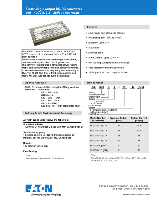
FeaturesHow to OrderAgency ApprovalsMilitary Grade Environmental Screening Notes:See “Guide to Operation” for full detailsNotes:Standard unit has pins out the top with 6-32 THD inserts,written as SL500SI/28-270• Input Range from 200Vdc to 400Vdc • No Derating from -55 C to +100 C • Efficiency: Up to 91%• Parallelable• Synchronizable• Power Density: Up to 87W / in�• Non-latching Overtemperature Protection • Fixed Frequency Power Conversion • Latching Output Overvoltage ProtectionSL 500 S I / 28 - C (270)SeriesTotal Output Power Single Output OptionsI - Unscreened M - Screened Output Voltage OptionsC - Thru Hole Inserts (0.140 DIA) I - Metric Inserts (M3)Input Voltage100% Environmental Screening for Military Versions Meets MIL – Standards: MIL – STD – 454 P4855 – 1A MIL – STD – 704D MIL – STD – 810E MIL – S – 901C MIL-STD- 461F with companion filter The SL500 converter is a standalone, 91% efficient COTS converter in a standard 2.4” x 4.6” x 0.52” full brick package.Protection features include overvoltage, overcurrent, overtemperature, and short circuit protection.The converter is parallelable for higher power require-ments and synchronizable for noise sensitive systems. A 300 KHz fixed switching frequency aids in filtering of EMI. The SL500 EMI filter is third party qualified and meets Mil-Std-461F for conducted emissions.All “Mil” Grade units receive the following:Stabilization Bake :+125 C for 24 hours per Mil-Std-883, M1108, Condition B Temperature Cycling :10 cycles at -55 C to +125 C (transition period 36 minutes) per Mil-Std-883, M1010, Condition B Burn-in :160 hours at +85 C min.Final TestingModel Number (Unscreened)SL500SI/28 (270)SL500SI/24 (270)SL500SI/15 (270)SL500SI/12 (270)SL500SI/5 (270)SL500SI/3.3 (270)Nominal Output(Vdc)2824151253.3Output Current(Amps)17.920.925254040/powerconversionFor additional information, call 310.542.8561ore-mail:*******************Input Characteristics - 270Vdc InputOutput CharacteristicsInput VoltageBrown Out (75%) Full Load No Load Power Dissipation Inrush Current <20µS Duration Reflected Ripple Current Logic Disable Current (Sink)Logic Disable Power In Input Ripple Rejection (120HZ)Efficiency Up ToInput Transient Per MIL-STD-704D (Operating 100ms)EMIMIN200185TYP 27027302.86091UNITS Vdc Vdc W A A rmsmA W dB %MAX 4000.52Use Companion FilterNote: Output Ripple is measured with 1µF ceramic and 22µF low ESR Tantalum CapacitorSet Point Accuracy Load Regulation Line Regulation Ripple P-P (20MHz)Trim Range Remote Sense 12V , 15V , 24V , 28V3.3V , 5VOvervoltage Protection Current Sharing Transient Response 50-75% Load (0.2A/µS)Temperature Drift Long Term Drift Current Limit Short Circuit Current Turn-on Time (Power Input)Logic Turn-on Time Switching Frequency Sync Input Voltage Sync Input Frequency Sync Input Duty Cycle Turn-on OvershootMIN90110254.533015TYP 11250.010.0215090300MAX 1±0.3±0.231100.500.25135±83/3000.030.05140755.5360550.1UNITS % Vout % Vout % Vout % Vout % Vout Vdc Vdc % Vout % Iout / at Full Load% Vout / µSSetting Time to Within 1% Vout%Vout / C %Vout / 1KHrs%Iout %Iout Hiccup TypemS FL 270V mS FL 270VKHzVp-p KHz %% Vout500VdcSpecificationsTemperature CharacteristicsMechanical CharacteristicsOperating (Baseplate)Storage (Ambient)Over Temperature Shutdown Thermal Resistance (Case to Ambient)MIN-55-55TYP +1055.71MAX +100+125+110UNITS C CC / Auto RecoveryC / WInput to Output Output to Base-plate Input to Base-plate Insulation Resistance (Measured at 50 VDC)Input to Output CapacitanceMIN1000500100050TYP 0.003MAX UNITS Vdc Vdc Vdc MohmµFWeight Size Volume Mounting (STD)ConstructionTYP7.62.4 x 4.6 x 0.5261 x 116.9 x 13.25.7494UNITS oz in mm in�cm�Threaded, #6-325 sided metal can, nickel plated cover, aluminum baseplateIsolation CharacteristicsCase drawingsCase Drawingsinch mmA 4.60116.9B 2.4061.0C .5213.2D 2.00050.80E .205.1F .205.1G .3759.53H 4.200106.68J .5012.7K .40010.20L .70017.8M 1.00025.40N 1.40035.60P.0401.02R .0802.03Standard ModelC OptionThru hole inserts (0.140 DIA)Model number written as SL500SI/28-C (270)Tolerances:Material: Mounting: 6-32 THD inserts are provided in baseplate Metric: M3 insertsInches mm x.xx = ±0.03x.xxx = ±0.015x.xx = ±0.4x.x = ±0.8Pin = Brass (Solder Plating)Baseplate = Aluminum 5050-H32Case = SteelFinish = Nickel PlatingPin placement on top of unitTOP VIEW(MARKING SURFACE)KLMNJB FHE DA12345678109P DIA ±0.005B A S E P L A T EINPUT PINSOUTPUT PINSG MINCR DIA ±0.005B A S E P L A T EG MINP DIA ±0.005CCharacteristicsCharacteristicsIX. TTL Turn OnIII. Ef ficiency vs. Input VoltageII. Efficiency vs. Output Power I. Input Voltage vs. Output PowerVI. Input Transient ResponseV. Load Transient ResponseIV. Output Voltage RippleVII. Input Inrush CurrentVIII. Input Current RippleX. TTL Turn OffXI. Turn OnXII. Turn OffO u t p u t P o w e r (%)Input Voltage VDC E f fi c i e n c y (%)E f fi c i e n c y (%)10090807017017518018540020406080100556065707580859095Output Power (%)Input Voltage VDC9492908886848280787620024028032036040050m V /d i v500m V /d i v5A /d i vTime: 2µS/divBandwidth: 20MHzV in = 270Vdc I out = 17.9A V out = 28VTime: 400µS/divV in = 270Vdc V out = 28VI out = 17.9A V out = 28V200m V /d i v100V /d i vTime: 400µS/div100V /d i v10A /d i vV in = 270Vdc I out = 17.9A V out = 28VTime: 10µS/div 2A /d i vTime: 2µS/div V in = 270Vdc I out = 17.9A V out = 28VV in = 270Vdc I out = 17.9A V out = 28VV in = 270Vdc I out = 17.9A V out = 28VV in = 270Vdc I out = 17.9A V out = 28VV in = 270Vdc I out = 17.9A V out = 28V Time: 400µS/divTime: 200µS/divTime: 20mS/divTime: 20mS/div2V /d i v5V /d i v5V /d i v5V /d i v100V /d i v5V /d i v100V /d i v10V /d i vFor example, if the DC/DC converter in Figure 1a is a50W unit (5VDC @ 10 Amps) with output load regulationspecified at 0.2%; the connection as shown will degradeload regulation by a factor of 10. In this example, the 4feet of #14 AWG wire used to connect the converteroutput to the load, has a total line resistance of 10mΩ(ignoring any contact resistance). For a 50W, 5 VDCoutput converter, the drop across the lead resistance willbe 100 mV (10A x 0.010Ω) or 2% of the output. Thus,the converter is selected for 0.2% regulation, but thepower system layout achieves only 2.2%.This can be corrected by decreasing the distancebetween the converter output and load. If that is notpossible, using larger diameter wire (see Table 1), orPCB runs that have larger cross sectional area andshorter length will also reduce conductor resistance. Theuse of the converter’s remote sense capability will alsowork (see Remote Sense for more information on thisoption).General Application NotesThe most basic use of the power converter is shown inFigure 1. An input fuse is always recommended toprotect both the source and the power supply in theevent of failures. Slow-blow fuse is recommended with acurrent rating approximately 200% of the full load inputcurrent to the converter. Having a slow-blow type fusewill allow for the converter’s inrush charge at turn-on.The sense pins of the converters must be connected totheir corresponding output bus. Inherently, powerconverters will have some internal energy loss, which isdissipated in the form of heat through an aluminummounting surface. This surface must be cooled tomaintain a temperature below the maximum operatingtemperature.Wire Gage & Distance to LoadIf the resistance of the wire, printed circuit board runs orconnectors used to connect a converter to systemcomponents is too high, excessive voltage drop will resultbetween the converter and system components, degrad-ing overall system performance.The SL family of power converters, designed as militarygrade standalone power converters, can also be used ascomponents in complex power systems. The SL Seriesutilizes a high efficiency full bridge isolated DC to DCconverter which operates at 300 KHz constant frequency.The SL units are supplied in five sided metal case tominimize radiated noise. A number of protectionfeatures, as well as electrical and thermal derating ofinternal components per NAVSO P3641A guidelines andthe use of proven topology allow for high reliabilitythroughout an operating range of -55 C to +100 C. Inapplications where even greater reliability is required, theconverter can be screened to MIL-STD-883 upon#AWG91011121314151617181920CurrentResistance(mΩ/Foot)0.7920.9981.2611.5882.0012.5243.1814.0205.0546.3868.04610.13#AWG212223242526272829303132CurrentResistance(mΩ/Foot)12.7716.2020.3025.6732.3741.0251.4465.3781.21103.7130.9162.0Table 1/powerconversionFor additional information, call 310.542.8561ore-mail:*******************General Application Notes - con’tRemote sense pins, +S and -S have been provided on the SL Series converters for applications where precise load regulation is required at a distance from where the converter is physically located. If remote sensing is NOT required, these pins MUST be tied to their repective output pins (+S to +OUT, -S to -OUT, see Figure 2). If one or more of these sense pins are not connected to their respective output pins, the output of the unit will not regulate to within specification and may cause high output voltage condition.Remote On / OffNOTE: High IR drops between the converter and load may cause converter parameters, such as output voltage accuracy, trim range, etc., to appear to be out of specification. High IR drops on input lines may cause start up problems (voltage at the input pins below the input range of the converter). Obviously, any connections made to the power distribu-tion bus present a similar problem. Poor connections (such as microcracking around solder joints) can cause serious problems such as arcing. Contact resistance must be minimized. Proper workmanship standards must be followed to insure reliable solder joints for board mount converters. Terminal strips, spade lugs and edge connectors must be free of any corrosion, dust or dirt. If parallel lines or connections are available for routingconverter output currents, they should be utilized. Remote SenseFigure 2DO NOT connect sense pins to any pin other than their respective output pins or permanent damage will occur. DO NOT connect sense pins to any load other than the same load the output pins are connected to or permanent damage may occur.Remote turn ON / OFF (TTL Pin) is an additional featureto the SL Series. This feature is especially useful inportable/mobile applications where battery powerconservation is critical. The voltage level at the TTL pinis referenced with respect to the converter’s –VIN Input.When the TTL pin is pulled to less than 1.0V with respectto the –VIN pin. Via either an open collector (see Figure3) or a mechanical switch with a 0.5mA capability, the converter shuts down. An optocoupler can also be usedIF the TTL Signals need to be referenced from the outputside. If the TTL pin is left floating the unit remains on.When multiple units are tied to a central switch com-mand, a series resistor of 200 Ohms to each TTL pin isrecommended to increase noise immunity.Figure 3 Output TrimThe output trim pin has been supplied on the SL familyto provide output voltages other than the nominal fixedvoltage. Output voltage can be increased or decreased(+10% Max, -10% Min) by simply connecting a resistorbetween the trim pin and the –Output return pin or the+Output pin respectively (see Figure 4).Figure 4Output Trim - con’tThe value of the resistors required to Trim Hi is shown in the Table 2. The external resistor is connected between the Trim Pin and the Output Return Pin at the power supply (use standard value 1% resistor closest to the table value). Trimming the output voltage too high may activate the over voltage protection circuitry. The value of resistor required to Trim Lo is shown in Table 2.The external resistor is connected between the Trim Pin and the +Output Pin at the power supply (use standard value 1% resistor closest to the table value). A potentiometer can be substituted for the resistor to achieve a more precise output voltage setting. When trimming up or down, the maximum output current and/or maximum output power cannot be exceeded.15Vout110% Vout 108% Vout 106% Vout 104% Vout 102% Vout 100% Vout 98% Vout 96% Vout 94% Vout 92% Vout 90% Vout Volts16.5016.2015.9015.6015.3015.0014.7014.4014.1013.8013.50KΩ122.9153.9205.1309.9616.8OPEN107.846.225.715.49.124VoutVolts26.4025.9225.4424.9624.4824.0023.5223.0422.5622.0821.60KΩ224.0278.6369.8554.91165OPEN103.744.724.614.48.328VoutVolts30.8030.2429.6829.1225.5628.0027.4426.8826.3225.7625.20KΩ268.6331.8435.9650.61282OPEN110.649.528.918.612.43.3Vout110% Vout 108% Vout 106% Vout 104% Vout 102% Vout 100% Vout 98% Vout 96% Vout 94% Vout 92% Vout 90% Vout Volts3.633.563.503.433.373.303.233.173.103.042.97KΩ8.3010.414.021.443.3OPEN115.357.137.527.421.45VoutVolts5.505.405.305.205.105.004.904.804.704.604.50KΩ18.324.836.158.1134.0OPEN106.948.928.418.312.212VoutVolts13.2012.9612.7212.4812.2412.0011.7611.5211.2811.0410.80KΩ92.6117.1158.1241.7504.6OPEN100.744.424.914.98.80Table 2Military SpecificationsSpecification MIL-STD-704D MIL-STD-810EMIL-S-901CConditionInput TransientVibrationHumidityTemperature/AltitudeAccelerationTemperature ShockHigh Impact ShockMethod514.4507.3520.1513.4503.3Procedure1133Test ConditionTransients up to 500V for 0.1 sec (270Vdc input)Up to 30 gs, each axis for 1 hour95% humidity, non condensing for 10 days40 hours from -55°C to +71°C14 gs each axis-55°C to + 100°C (non-operating, one hour each cycle)5 foot hammer dropSeries OperationSynchronizationThe SL500 family of power converters may be arranged in a series operating mode to supply higher outputvoltages when required (see Figure 5). In this configura-tion, D1 and D2 are added to protect against the applica-tion of a negative across the outputs of the powerconverters during power up and power down. The two (or more) units do not need to have the same output voltage, but the output current supplied in this configura-tion will be limited to the lowest maximum output current of the modules used.Synchronization of switch-mode converters to a central system clock frequency is often essential in noise sensitive systems. The SL Series can be tied to the central clock that is referenced to -OUT (see Figure 7) by inputting a square wave clock signal which has a frequency amplitude and duty cycle within specifiedlimits. The SL Series converter’s internal synchonization circuit is triggered by rising edge of this clock waveform.DO NOT add any capacitance from the SYNC pin line to Ground.Parallel OperationThe SL500 converter family has the capability of being paralleled to drive loads of higher power than a single SL500 unit can handle. The PAR pin is supplied on the unit for this function (see Figure 6). If parallel operation of two or more units is removed, the following precau-tions must be followed:• Corresponding input and output leads or traces on each unit should be as equal in length and size aspractical. The more equivalent the leads are, the closer the unit sharing.• The PAR pins of all units should be tied together.The units do not have to be synchronized for parallel operation but may be if required (see Synchronization ). Or’ing diodes may be included in the positive output leads for true N + 1 redundant systems, but are not necessary. Local sensing should be used whenever possible to minimize noise on the +S and -S pins in parallel applications.Figure 6Parallel OperationSynchronization to External ClockOutput ripple and noise (sometimes referred to as PARDor “Periodic and Random Deviations”) can be defined as unwanted variations in the output voltage of a power supply. In switching power supplies, this output noise is seen as a series of pulses with a high frequency content and is therefore measured as a peak value (i.e., speci-fied as “peak-to-peak”).Ripple & NoiseRipple & Noise - con’tElectro Magnetic Filter (EMI) - SLF500The SL Series of power supplies are specified and tested in our factory with a 20 MHz bandwidth oscillo-scope / probe. Measurements taken by a scope set at higher frequencies (i.e. 300 MHz) may produce signifi-cantly different results due to noise coupling on to the probe from sources other than the power supply. Noise that is common to all output leads of a power converter with repect to the chassis is refered to as common mode noise. Noise that is apparent on one output lead with respect to the other output lead is referred to as differential mode noise. Common mode noise is produced in switching action. Martek Power, a brand of Cooper Bussmann, typically minimizes the level of output common mode noise by incorporating line to chassis ground capacitors (on input and output leads) into the power converters. In most cases, this issufficient to minimize the level of common mode noise. However, if further attenuation is required, additional line to chassis ground capacitance may be added by the customer at the system level. Martek Power noisespecifications (output ripple specifications) all reference the level of differential mode noise at a given bandwidth, not the level of common mode noise. The measurement of differential mode noise is detailed in the following paragraphs.Measurement TechniquesThe length of all measurement leads (especially the ground lead) should be minimized and the sense pins should be tied to their respective outputs (+SENSE to +OUTPUT, - SENSE to - OUTPUT). One inch or less from the output terminals, place a ceramic capacitor of 1µF and a 22µF low ESR Tantalum capacitor. Using an X1 scope probe with a 20 MHz bandwidth, we recom-mend measurement close to the capacitors. We do not recommend using the probe ground clip. Instead,replace it with connecting a short bus wire (generally 0.5 inches or less, making a loop at the end to place the probe in) to the negative and positive outputs on the backside of the connector. Place the tip of the probe on the +OUTPUT, and the ground ring (or ground band) on the -OUTPUT for a true ripple measurement (see Figure 8). Utilizing the probe ground ring (as opposed to a ground clip) will minimize the chance of noise coupling from sources other than the power supply.Figure 8Sense Tied Local+ SENSE + OUTPUT1” max.- SENSE- OUTPUT 1µF 22µFRipple and Noise Test Set-UpMaximum Allowable CapacitanceOutput Voltage3.3V 5V 12V 15V 24V 28VMax Capacitance15,000µF 15,000µF 5,000µF 5,000µF 3,000µF 3,000µFFor applications where electromagnetic interference is a concern, the SLF500, a passive input line filter may be installed at the input of the SL Series converters (see Figure 9). If output power greater than 500 watts are required, multiple SLF500 units will be necessary. For more details, consult the factory.Figure 9Table 3Ripple Reduction TechniquesIn applications where the output ripple of the converter is higher than desired, various techniques can beemployed to reduce output ripple and noise (PARD). One method is to add additional capacitance in parallel with the output leads of the converter (low ESR type tantalums or ceramic are recommended). This should substantially reduce PARD. See Table 3 for maximum allowable capacitance that may be added to the output leads.SLF500 SchematicSL500 Block DiagramINPUTVDCOUTPUTTTL ON/OFF/powerconversionEaton is a registered trademark. All other trademarks are property of their respective owners.Eaton1000 Eaton Boulevard Cleveland, OH 44122 United States © 2017 EatonAll Rights Reserved Printed in USA March 2017ore-mail:*******************。
DCDC培训资料2

按变换类型分类
按开关类型分类
DC/DC转换器按变换类型可分为直接 和间接两种。直接DC/DC转换器通过 开关管和储能元件实现电压的直接变 换,间接DC/DC转换器则通过变换器 将直流电源转换为交流电源,再通过 整流和滤波电路实现直流电源的变换 。
DC/DC转换器按开关类型可分为硬开 关和软开关两种。硬开关在开关过程 中因器件的硬性开通和关断而产生较 大的损耗和电磁干扰,而软开关则在 开关过程中通过谐振技术使开关器件 在零电压或零电流状态下进行开关转 换,从而降低了损耗和电磁干扰。
航空航天领域
航空航天领域需要使用DC/DC转换器将母线电压 转换为各种电子设备所需的直流电源,同时由于 空间环境的特殊性,要求DC/DC转换器具有较高 的可靠性和稳定性。
工业控制系统
工业控制系统中需要使用大量的传感器、执行器 和控制器等电子设备,这些设备需要使用DC/DC 转换器提供稳定可靠的电源。
升压(Boost)电路
采用电容器存储能量,然后与输入电压一起向 负载提供能量,使得输出电压大于输入电压。
反转(Inverter)电路
3
将直流电压转换成交流电压,通常用于无源元 件的驱动。
DC/DC转换器的控制方式
01
脉冲宽度调制( PWM)
通过调节占空比来控制输出电压,使 得输出电压保持稳定。
02
定期对DC/DC转换器进行维护 检查,包括清理灰尘、检查电 路板和散热风扇等,确保设备 正常运行
DC/DC转换器的优化方向及改进措施
优化方向:提高转换效率 改进措施:增加过压保护功能
通过优化电路设计和选用高效元器件,提高DC/DC转 换器的转换效率
在DC/DC转换器上增加过压保护功能,当输出电压过 高时,能够自动切断电源,保护负载和电路板
- 1、下载文档前请自行甄别文档内容的完整性,平台不提供额外的编辑、内容补充、找答案等附加服务。
- 2、"仅部分预览"的文档,不可在线预览部分如存在完整性等问题,可反馈申请退款(可完整预览的文档不适用该条件!)。
- 3、如文档侵犯您的权益,请联系客服反馈,我们会尽快为您处理(人工客服工作时间:9:00-18:30)。
Maxim > Design Support > Technical Documents > Tutorials > Power-Supply Circuits > APP 2031Keywords: DC to DC, buck, boost, flyback, inverter, PWM, quick-PWM, voltage mode, current mode skip, synchronous rectifier, switching regulator, linear regulatorTUTORIAL 2031DC-DC Converter TutorialNov 29, 2001Abstract:Switching power supplies offer higher efficiency than traditional linear power supplies. They can step-up, step-down, and invert. Some designs can isolate output voltage from the input. This article outlines the different types of switching regulators used in DC-DC conversion. It also reviews and compares the various control techniques for these converters.IntroductionThe power switch was the key to practical switching regulators. Prior to the invention of the Vertical Metal Oxide Semiconductor (VMOS) power switch, switching supplies were generally not practical.The inductor's main function is to limit the current slew rate through the power switch. This action limits the otherwise high-peak current that would be limited by the switch resistance alone. The key advantage for using an inductor in switching regulators is that an inductor stores energy. This energy can be expressed in Joules as a function of the current by:E = ½ × L × I²A linear regulator uses a resistive voltage drop to regulate the voltage, losing power (voltage drop times the current) in the form of heat. A switching regulator's inductor does have a voltage drop and an associated current but the current is 90 degrees out of phase with the voltage. Because of this, the energy is stored and can be recovered in the discharge phase of the switching cycle. This results in a much higher efficiency and much less heat.What is a Switching Regulator?A switching regulator is a circuit that uses a power switch, an inductor, and a diode to transfer energy from input to output.The basic components of the switching circuit can be rearranged to form a step-down (buck)converter, a step-up (boost) converter, or an inverter (flyback). These designs are shown in Figures 1,2,3, and 4 respectively, where Figures 3 and 4 are the same except for the transformer and the diode polarity. Feedback and control circuitry can be carefully nested around these circuits to regulate the energy transfer and maintain a constant output within normal operating conditions.Figure 1. Buck converter topology.Figure 2. Simple boost converter.Figure 3. Inverting topology.Figure 4. Transformer flyback topology.Why Use a Switching Regulator?Switching regulators offer three main advantages compared to linear regulators. First, switching efficiency can be much better. Second, because less energy is lost in the transfer, smaller components and less thermal management are required. Third, the energy stored by an inductor in a switching regulator can be transformed to output voltages that can be greater than the input (boost), negative (inverter), or can even be transferred through a transformer to provide electrical isolation with respect to the input (Figure 4).Given the advantages of switching regulators, one might wonder where can linear regulators be used? Linear regulators provide lower noise and higher bandwidth; their simplicity can sometimes offer a less expensive solution.There are, admittedly, disadvantages with switching regulators. They can be noisy and require energymanagement in the form of a control loop. Fortunately, the solution to these control problems is integrated in modern switching-mode controller chips.Charge PhaseA basic boost configuration is depicted in Figure 5. Assuming that the switch has been open for a long time and that the voltage drop across the diode is negative, the voltage across the capacitor is equal to the input voltage. When the switch closes, the input voltage, +V IN, is impressed across the inductor and the diode prevents the capacitor from discharging +V OUT to ground. Because the input voltage is DC, current through the inductor rises linearly with time at a rate proportional to the input voltage divided by the inductance.Figure 5. Charging phase: when the switch closes, current ramps up through the inductor.Discharge PhaseFigure 6 shows the discharge phase. When the switch opens again, the inductor current continues to flow into the rectification diode to charge the output. As the output voltage rises, the slope of the current, di/dt, though the inductor reverses. The output voltage rises until equilibrium is reached or:V L = L × di/dtIn other words, the higher the inductor voltage, the faster the inductor current drops.Figure 6. Discharge phase: when the switch opens, current flows to the load through the rectifying diode.In a steady-state operating condition, the average voltage across the inductor over the entire switching cycle is zero. This implies that the average current through the inductor is also in steady state. This is an important rule governing all inductor-based switching topologies. Taking this one step further, we can establish that for a given charge time, t ON, and a given input voltage and with the circuit in equilibrium, there is a specific discharge time, t OFF, for an output voltage. Because the average inductor voltage in steady state must equal zero, we can calculate for the boost circuit:V IN × t ON = t OFF × V LAnd because:V OUT = V IN + V LWe can then establish the relationship:V OUT = V IN × (1 + t ON/t OFF)Using the relationship for duty cycle (D):t ON/(t ON + t OFF) = DThen for the boost circuit:V OUT = V IN/(1-D)Similar derivations can be made for the buck circuit:V OUT = V IN × DAnd for the inverter circuit (flyback):V OUT = V IN × D/(1-D)Control TechniquesFrom the derivations for the boost, buck, and inverter (flyback), it can be seen that changing the duty cycle controls the steady-state output with respect to the input voltage. This is a key concept governing all inductor-based switching circuits.The most common control method, shown in Figure 7, is pulse-width modulation (PWM). This method takes a sample of the output voltage and subtracts this from a reference voltage to establish a small error signal (V ERROR). This error signal is compared to an oscillator ramp signal. The comparator outputs a digital output (PWM) that operates the power switch. When the circuit output voltage changes, V ERROR also changes and thus causes the comparator threshold to change. Consequently, the output pulse width (PWM) also changes. This duty cycle change then moves the output voltage to reduce the error signal to zero, thus completing the control loop.Figure 7. Varying error signal generates a pulse-width-modulated switch signal.Figure 8 shows a practical circuit using the boost topology formed with the MAX1932. This IC is an integrated controller with an onboard programmable digital-to-analog converter (DAC). The DAC sets the output voltage digitally through a serial link. R5 and R8 form a divider that meters the output voltage. R6 is effectively out of circuit when the DAC voltage is the same as the reference voltage (1.25V). This is because there are zero volts across R6 and so zero current. When the DAC output is zero (ground), R6 is effectively in parallel with R8. These two conditions correspond to the minimum and maximum output adjustment range of 40V and 90V, respectively.Figure 8. The MAX1932 provides an integrated boost circuit with voltage-mode control.Next, the divider signal is subtracted from the internal 1.25V reference and then amplified. This error signal is then output on pin 8 as a current source. This, in conjunction with the differential input pair, forms a transconductance amplifier. This arrangement is used because the output at the error amp is high impedance (current source), allowing the circuit's gain to be adjusted by changing R7 and C4. This arrangement also provides the ability to trim the loop gain for acceptable stability margins. The error signal on pin 8 is then forwarded to the comparator and output to drive the power switch. R1 is a current-sense resistor that meters the output current. When the current is unacceptably high, the PWM circuit shuts down, thereby protecting the circuit.The type of switching (topology) in Figures 7 and 8 is classified as a voltage-mode controller (VMC) because the feedback regulates the output voltage. For analysis we can assume that if the loop gain is infinite, the output impedance for an ideal voltage source is zero. Another commonly used type of control is current-mode control (CMC). This method regulates the output current and, with infinite loop gain, the output is a high-impedance source. In CMC, the current loop is nested with a slower voltage loop, as shown in Figure 9; a ramp is generated by the slope of the inductor current and compared with the error signal. So, when the output voltage sags, the CMC supplies more current to the load. The advantage of CMC is its ability to manage the inductor current. In VMC the inductor current is not metered. This becomes a problem because the inductor, in conjunction with the output filter capacitor, forms a resonant tank that can ring and even cause oscillations. Current mode control senses the inductor current to correct for inconsistencies. Although difficult to accomplish, carefully selected compensation components can effectively cancel out this resonance in VCM.Figure 9. Current-mode pulse-width modulation.The circuit in Figure 10 uses CMC with the MAX668 controller. This boost circuit is similar to Figures 7 and 8 except that R1 senses the inductor current for CMC. R1 and some internal comparators provide a current limit. R5 in conjunction with C9 filters the switching noise on the sense resistor to prevent false triggering of the current limit. The MAX668's internal current-limit threshold is fixed; changing resistor R1 adjusts the current-limit setting. Resistor R2 sets the operating frequency. The MAX668 is a versatile integrated circuit that can provide a wide range of DC-DC conversions.The external components of the MAX668 can have high-voltage ratings that provide greater flexibility for high-power applications. For portable applications that require less power, the MAX1760 and theMAX8627 are recommended. These latter devices use internal FETs, and sense the current by using the FETs' resistance to measure inductor current (no sense resistor required).Figure 10. The MAX668 for current-mode-controlled boost circuit.Figure 11 shows a simplified version of Maxim's Quick-PWM™ architecture. To analyze this buck circuit, we start with the feedback signal below the regulating threshold defined by the reference. If there are no forward current faults, then the t ON one-shot timer that calculates the on-time for DH is turned on immediately along with DH. This t ON calculation is based on the output voltage divided by the input, which approximates the on-time required to maintain a fixed switching frequency defined by the constant K. Once the t ON one-shot timer has expired, DH is turned off and DL is turned on. Then if the voltage is still below the regulating threshold, the DH immediately turns back on. This allows the inductor current to rapidly ramp up to meet the load requirements. Once equilibrium with the load has been met, the average inductor voltage must be zero. Therefore we calculate:Figure 11. Simplified block diagram of Maxim's Quick-PWM control.t ON × (V IN - V OUT) = t OFF × V OUTRearranging:V OUT/(V IN - V OUT) = t ON/t OFFAdding 1 to both side and collecting terms:V OUT/V IN = t ON/(t ON + t OFF)Because the duty factor is D:t ON/(t ON + t OFF) = DFor the buck circuit:D = V OUT/V INMaxim's proprietary Quick-PWM control method offers some advantages over PWM. Quick-PWM control generates a new cycle when the output voltage falls below the regulation threshold. Consequently, heavytransients force the output to fall, immediately firing a new on-cycle. This action results in a 100ns load-step response. It is also important to note that unlike the buck circuit in Figure 1, Figure 11 uses a MOSFET (Q2) instead of a diode for the discharge path. This design reduces the losses associated with the diode drop; the on-resistance of the MOSFET channel doubles as a current sense. Because output-voltage ripple is required to stimulate the circuit to switch, an output filter capacitor with some ESR is required to maintain stability. The Quick-PWM architecture can also respond quickly to line input changes by directly feeding the input voltage signal to the on-time calculator. Other methods must wait for the output voltage to sag or soar before action is taken, and this is often too late.A practical application of Quick-PWM is found in Figure 12. The MAX8632 is an integrated DDR memory power supply. Along with a Quick-PWM buck circuit (VDDQ), the MAX8632 integrates a high-speed linear regulator (VTT) to manage bus transients found in DDR memory systems. The linear regulator offers specific advantages over switchers: linear regulators do not have an inductor to limit current slew-rate, so a very fast current slew rate can service load transients. Slower circuits would require large capacitors to provide load current until the power supply can ramp up the current to service the load.More detailed image (PDF, 76kB)Figure 12. The MAX8632 uses Maxim's Quick-PWM architecture and a linear regulator to provide a complete DDR power-supply system. The device can be used as a main GPU or as a standard core-logic power supply.EfficiencyOne of the largest power-loss factors for switchers is the rectifying diode. The power dissipated is simply the forward voltage drop multiplied by the current going through it. The reverse recovery for silicon diodes can also create loss. These power losses reduce overall efficiency and require thermal management in the form of a heat sink or fan.To minimize this loss, switching regulators can use Schottky diodes that have a relatively low forward-voltage drop and good reverse recovery. For maximum efficiency, however, you can use a MOSFET switch instead of the diode. This design is known as a "synchronous rectifier" (see Figures 11, 12 and 13). The synchronous rectifier switch is open when the main switch is closed, and the same is true conversely. To prevent cross-conduction (both top and bottom switches are on simultaneously), the switching scheme must be break-before-make. Because of this, a diode is still required to conduct during the interval between the opening of the main switch and the closing of the synchronous-rectifier switch(dead time). When a MOSFET is used as a synchronous switch, the current normally flows in reverse (source to drain), and this allows the integrated body diode to conduct current during the dead time. When the synchronous rectifier switch closes, the current flows through the MOSFET channel. Because of the very low-channel resistance for power MOSFETs, the standard forward drop of the rectifying diode can be reduced to a few millivolts. Synchronous rectification can provide efficiencies well above 90%.Figure 13. Synchronous rectification for the buck circuit. Notice the integrated MOSFET body diode.Skip Mode Improves Light Load EfficiencyA feature offered in many modern switching controllers is skip mode. Skip mode allows the regulator to skip cycles when they are not needed, which greatly improves efficiency at light loads. For the standard buck circuit (Figure 1) with a rectifying diode, not initiating a new cycle simply allows the inductor current or inductor energy to discharge to zero. At this point, the diode blocks any reverse-inductor current flow and the voltage across the inductor goes to zero. This is called "discontinuous mode" and is shown in Figure 14. In skip mode, a new cycle is initiated when the output voltage drops below the regulating threshold. While in skip mode and discontinuous operation, the switching frequency is proportional to the load current. The situation with a synchronous rectifier is, unfortunately, somewhat more complicated. This is because the inductor current can reverse in the MOSFET switch if the gate is left on. TheMAX8632 integrates a comparator that senses when the current through the inductor has reversed and opens the switch, allowing the MOSFET's body diode to block the reverse current.Figure 14. In discontinuous mode the inductor fully discharges and then the inductor voltage rests at zero.Figure 15 shows that skip mode offers improved light-load efficiencies but at the expense of noise,because the switching frequency is not fixed. The forced-PWM control technique maintains a constant switching frequency, and varies the ratio of charge cycle to discharge cycle as the operating parameters vary. Because the switching frequency is fixed, the noise spectrum is relatively narrow, thereby allowing simple lowpass or notch filter techniques to greatly reduce the peak-to-peak ripple voltage. Because the noise can be placed in a less-sensitive frequency band, PWM is popular with telecom and other applications where noise interference is a concern.Figure 15. Efficiency with and without skip mode.SummaryAlthough switching techniques are more difficult to implement, switching circuits have almost completely replaced linear power supplies in a wide range of portable and stationary designs. This is because switching circuits offer better efficiency, smaller components, and fewer thermal management issues. MOSFET power switches are now integrated with controllers to form single-chip solutions, like theMAX1945 circuit shown in Figure 16. This chip has a metallic slug on the underside that removes heat from the die so the 28-pin TSSOP package can dissipate over 1W, allowing the circuit to supply over 10W to its load. With a 1MHz switching frequency, the output inductor and filter capacitors can be reduced in size, further saving valuable space and component count. As MOSFET power-switch technologies continue to improve, so will switch-mode performance, further reducing cost, size, and thermal management problems.Figure 16. The MAX1945 is a 6A internal switch device with a reduced part count and small footprint to save board space.Part Selection LinksStep-Up/Boost ConvertersStep-Down/Buck ConvertersSwitching Regulators for Driving LEDsSwitching Regulators for Battery-Powered ApplicationsSwitching Regulators for Industrial (High Voltage) ApplicationsRelated PartsMAX17600.8A, Low-Noise, 1MHz, Step-Up DC-DC Converter Free SamplesFree Samples MAX1932Digitally Controlled, 0.5% Accurate, Safest APD BiasSupplyMAX19451MHz, 1% Accurate, 6A Internal Switch Step-DownFree SamplesRegulatorsMAX668 1.8V to 28V Input, PWM Step-Up Controllers in µMAX Free SamplesFree Samples MAX8627Low V BATT, 20µA I Q, 1MHz Synchronous BoostConverter with True ShutdownFree Samples MAX8632Integrated DDR Power-Supply Solution for Desktops,Notebooks, and Graphic CardsMore InformationFor Technical Support: /supportFor Samples: /samplesOther Questions and Comments: /contactApplication Note 2031: /an2031TUTORIAL 2031, AN2031, AN 2031, APP2031, Appnote2031, Appnote 2031© 2013 Maxim Integrated Products, Inc.Additional Legal Notices: /legal。