L6598高功率IC
家电维修-全尺寸液晶电视和等离子电视电源解决方案

全尺寸液晶电视和等离子电视 电源解决方案目录传统电源:60W 开关电源(SMPS )(<20吋) 200W SMPS (最大 30-32吋)谐振电源:70W SMPS (<20吋) 180W SMPS (最大30吋) 500W SMPS (最大50吋 LCD-TV, 42吋 PDP-TV)60W 液晶电视(LCD-TV) 电源: 块图•工作模式接近CCM 和DCM之间的界 限:可变工作频率Vac电源单元EMI 滤波器和 桥接整流器 +12V•导通时零压开关/零 流开关 •EMI干扰不强 •可变扩展频谱 •启用待机功能先进的PWM控 制器反馈60W LCD-TV 电源: 技术规格宽输入电压: 90-265VAC 单输出电压 (Vout): Vout 电流 说明12V 5A 器件内的精确的过流和过压保护电路可 以选装。
.总输出功率: 60W60W LCD-TV 电源:电路图L656560W LCD-TV 电源: 测试报告负载效率测试负载 输出 全负载 (FL) 待机 无负载 测试结果 输入电压 全负载效率 待机 90V 100V 240V 264V 81.7% 83.2% 87.0% 87.4% 输入功率 无负载 12V 5A 0.0416A (0.5W) 0A一台60W LCD-TV 电源L6565: 准谐振开关电源控制器• 电流式准谐振PWM 控制器 • 微功率启动电流 (40µA 典型) • 小静态电流 (3mA典型值) • 谐振工作/外部数据同步ZCD 输 入 • 频率反馈功能 • 线路电压正向功能 • 逐脉冲过流保护 • 第二个电流级和打嗝模式工作 • 禁用功能 •电流读取上的内部RC滤波器 • 封装: Minidip 和SO8准谐振(QR)转换 : 准谐振概念Llk & CdLp Lm Ls VoutLp & C d VDSVDS @ Vin2 >VinCinLlk VRVin2VinVinCd VDSNO ZVS! Ip IPKs Pri Sec tZVSIs @ Vin2 >Vin工作模式接近CCM和DCM之间的界限:可 变工作频率 导通时零压开关(ZVS)/零流开关(ZCS) EMI干扰不强 可变扩展频谱IPKpIp @ Vin2 >VinTON T = 1/ fswTFWTvZVS 条件: Vin ≤ VR200W LCD-TV 电源: 块图•PFC(功率因数校正器)电源VacEMI 滤波器 和桥接整流 器200W 临界控制模 式,具备ZCD(零流 检测)功能,注重成 本效益 •主变换器 200W逆向变换器, 用于中等尺寸的 LCD-PDP/TV应用 •备用变换器 10W 逆变换器,内 置场效应MOS控制 器,和关断电路+24V+12V PFC+PWM+Aux L6562+L5991 +L6590 DC DC 变换器 +5V反馈 +5V 备 用变换200W LCD-TV 电源:技术规格5V 输出使用的DC-DC 变换器可以选择。
L6599中文资料

L6599中文资料1,Css软启动:连接一个外部电容到地,和一个电阻到RFmin到第4脚,用以设置最大振荡频率和为频率切换设定时间常数,以及芯片启动(软启动)。
当V cc<UVLO,Line<1.25V or >6V,DIS>1.85V,Isen>1.5V,Delay>3.5V时,一个内部开关会给这个电容放电,使芯片关闭,为下一个软启动作准备。
2,Delay延时:过电流延时关机,一个电容和一个电阻接在1脚与地之间,设置过流条件下的最大持续时间(从IC开始延时到IC关断),每当Isen脚上的电压超过0.8V时,其电容会由内部电流发生器充电(150uA),并由外部电阻缓慢放电,如果此电压超过2V,软启动电容就完全地放电,所以开关频率会推高到最高大值,150uA电流一直连续。
如果此电压超过3.5V,IC会关断,其内部电流发生器了也会关断,从而该点电压下降(因为外部电阻),当该点电压下降到低于0.35V时,IC会重新启动,因此,在短路条件下转换器会工作在间歇状态,输入平均功率非常低。
3,CF,时间电容:一个电容接在此脚与地之间,由内部电流发生器充电或放电,以此确定转换器的开关频率。
4,RFmin,设置最小的振动荡频率:此脚提供一下精确的2V参考电压,一个电阻接在此脚与地之间确定一个电流,此电流用来设定最小振动荡频率。
关闭反馈回路,通过调节振荡频率来调节转换器输出电压,光耦的光电三极管通过串联一个电阻接到此脚,此电阻将设定最大工作频率,一个R-C串联接于此脚与地之间,防止过多的能量涌入。
5,Stby,爆发模式工作门槛:此脚检测反馈控制电压,使之与一个内部参考电压(1.25V)比较,如果此脚电压低于参考电压,IC会进入空闭状态,静态电流会减少。
当此脚电压超过参考电压50mA时,IC会重启动,软启动不调节,如果不启用跳跃模式,应将此脚与RFmin脚联结在一起。
6,Isen,电流检测输入:此脚检测初级电流(通过一个电阻或一个电容无损的检测)。
长虹液晶彩电常见开关电源维修资料

长虹液晶彩电常见开关电源维修资料长虹液晶彩电HS210-4N02-2开关电源维修资料长虹液晶彩色电视采用HS210-4NO2-2电源板,该电源板可直接代换长虹GP09,HS210-4N10,FSP205-3E01C电源板,对+12V输出电路稍加改动,可以代换GP02,FSP205-4EOIC,FSP179-4F01电源板。
长虹HS280-4NO1,HS280-4NO2,HS308-4NO1,HS368-4NO1的主电源均采用NCP1395,NCP5181系列集成电路,均可参照本节维修。
HS210-4NO2-2电源板由三部分组成:一是由NCP1014P100(U1)和变压器T1组成的副开关电源,为微处理器控制系统提供+5.4VS电压;二是由NCP1606BDR2G(U2)和变压器T3组成的PFC 电路,为主开关电源提供+380V电压;三是由NCP1395DR2G (U4),NCP5181DR2G(U3)和变压器TZ组成的主开关电源,向负载主板和背光灯板电路提供24V和12V,5.25V电压。
开关机采用控制PFC电路和主开关电源的VCC1供电的方式,开机后以NCP1014P100为核心的副电源首先工作,输出两种电压:一是为主板控制系统提供5.4VS电压,控制系统工作后为电源板送入开机STB控制电压,二是副电源输出VCC电压,经开关机电路控制后,为PFC驱动电路NCP1606BDR2G和主电源驱动电路NCP1395DR2G 提供VCC1工作电压,PFC电路和主电源电路启动工作,市电整流滤波后VA约300V经PFC电路校正后,提升到约380V,产生VB电压,为主电源供电。
主电源工作后,为主电路板和背光灯逆变器板提供5.25V,12V和24V电源,整机进入开机收看状态。
长虹液晶彩色电视HS210-4NO2-2电源板在主开关电源输出端设有24V,12V,5.25V过电压保护和5.25V过电流保护电路,保护电路启动时,迫使开关电源停止工作。
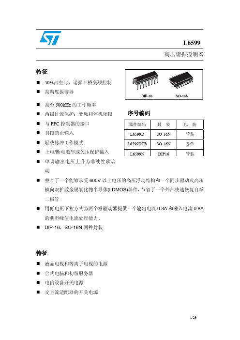
L6599-高压谐振控制器芯片-中文资料

L6599高压谐振控制器特征50%占空比,谐振半桥变频控制 高精度振荡器高至500kHz 的工作频率 序号编码器件编码封 装包 装L6599D SO-16N 管装 L6599DTR SO-16N 卷带 L6599NDIP16管装两级过流保护:变频和停机闭锁 与PFC 控制器的接口 自锁禁止输入 轻载脉冲工作模式上电/断电顺序或欠压保护输入 单调输出电压上升为非线性软启动整合了一个能够承受600V 以上电压的高压浮动结构和一个同步驱动式高压横向双扩散金属氧化物半导体(LDMOS)器件,节省了一个外部快速恢复自举二极管用低电压下拉方式为两个栅驱动器提供一个输出电流0.3A 和灌入电流0.8A的典型峰值电流处理能力。
DIP-16,SO-16N 两种封装特征液晶电视和等离子电视的电源 台式电脑和初级服务器 电信设备开关电源 交直流适配器的开关电源框图目录1 驱动描述 . . . . . . . . . . . . . . . . . . . . . . . . . . . . . . . . . . . . . . . . . . . . . . . . . .42 引脚设置 . . . . . . . . . . . . . . . . . . . . . . . . . . . . . . . . . . . . . . . . . . . . . . . . . .52.1 引脚排列 . . . . . . . . . . . . . . . . . . . . . . . . . . . . . . . . . . . . . . . . . . . . . . . . . . . .52.2 引脚功能说明 . . . . . . . . . . . . . . . . . . . . . . . . . . . . . . . . . . . . . . . . . . . . . . . . 53 典型系统框图 . . . . . . . . . . . . . . . . . . . . . . . . . . . . . . . . . . . . . . . . . . . . . . 74 电气数据 . . . . . . . . . . . . . . . . . . . . . . . . . . . . . . . . . . . . . . . . . . . . . . . . . . 74.1 极限参数. . . . . . . . . . . . . . . . . . . . . . . . . . . . . . . . . . . . . . . . . . . . . . . . . . . . . .74.2 热相关数据. . . . . . . . . . . . . . . . . . . . . . . . . . . . . . . . . . . . . . . . . . . . . . . . . . . . .85 电气参数. . . . . . . . . . . . . . . . . . . . . . . . . . . . . . . . . . . . . . . . . . . . . . . . . . . 96 典型的电气性能. . . . . . . . . . . . . . . . . . . . . . . . . . . . . . . . . . . . . . . . . . . . . .127 应用资料. . . . . . . . . . . . . . . . . . . . . . . . . . . . . . . . . . . . . . . . . . . . . . . . . . . 157.1 振荡器. . . . . . . . . . . . . . . . . . . . . . . . . . . . . . . . . . . . . . . . . . . . . . . . . . . . . . .167.2 工作在空载或非常轻的负载状态. . . . . . . . . . . . . . . . . . . . . . . . . . . . . . . . . . .187.3 软启动. . . . . . . . . . . . . . . . . . . . . . . . . . . . . . . . . . . . . . . . . . . . . . . . . . . . . . . .217.4 电流检测,过流保护和过载保护 . . . . . . . . . . . . . . . . . . . . . . . . . . . . . . . . . 237.5 闭锁关机. . . . . . . . . . . . . . . . . . . . . . . . . . . . . . . . . . . . . . . . . . . . . . . . . . . . . .267.6 LINE检测功能. . . . . . . . . . . . . . . . . . . . . . . . . . . . . . . . . . . . . . . . . . . . . . . . . .277.7 自举部分 . . . . . . . . . . . . . . . . . . . . . . . . . . . . . . . . . . . . . . . . . . . . . . . . . . . .287.8 应用实例. . . . . . . . . . . . . . . . . . . . . . . . . . . . . . . . . . . . . . . . . . . . . . . . . . . . .298 封装外形尺寸 . . . . . . . . . . . . . . . . . . . . . . . . . . . . . . . . . . . . . . . . . . . . . . . . .9 修订记录 . . . . . . . . . . . . . . . . . . . . . . . . . . . . . . . . . . . . . . . . . . . . . . . . . . . .1 驱动描述L6599是一个用于谐振半桥拓扑电路的精确的双端控制器。
电源IC L6668 L6563 L6599 L6566

3 VCOMP
4
Fix. Fre q .
突发模式 B u rs t Mo d e
Fre q u e n cy Fo ld b a ck Mo d e
Fix. Fre q .
t
固定频率模式 13 ST-BY 8 Vref RA 16 RCT CT RB
Mo d e
L6668
平滑的降频模式,可用一个外部电阻设置 在中低负载下能效最佳 在低负载或无负载下进入间歇模式,阈压可
115V低负载输入功率 115V low load input power Low load input power requirement 低负载输入功率要求
230V低负载输入功率 230V low load input power
115Vac efficiency 115Vac能效 90.0 85.0 80.0 75.0 70.0 65.0 60.0 55.0 50.0 0.0 1.0 2.0 3.0 4.0 5.0 6.0 7.0
无负载下间歇模式 斜率补偿 连接功率因数校正 IC的通信线路 闩锁关断过压/过热保护 软启动可编程 封装: SO-16
HY S T. CTRL + 0 .4 mA 13
PFC_ S TO P 14
D IS OCP
+
2 .2 /2 .7 V
S TA NDBY 11R 0 .8 V 9 S KIPA DJ SS 4R S O FT- S TA RT 11 10 CO MP
4 .5 V
10 O S C IL L AT O R MO D E S E L E C T IO N S R Q D R IVE R
MO D E /S C
l6599芯片工作原理 -回复
l6599芯片工作原理-回复l6599芯片是一款特殊的开关电源控制芯片,主要用于拓扑结构为半桥或全桥的开关电源电压模式控制。
本文将详细介绍l6599芯片的工作原理,并一步一步回答有关该主题的问题。
一、开关电源基本原理开关电源是一种将输入电压通过开关元件进行周期性开关,并通过滤波器和稳压电路获得所需电压的电源。
它具有高效率、体积小、重量轻的优点,广泛应用于各个领域。
开关电源主要由输入端、变压器、整流滤波电路、开关元件、控制电路和输出端组成。
二、l6599芯片介绍l6599芯片是一种高压开关电源控制芯片,采用双极型技术,适用于半桥、全桥拓扑结构的开关电源。
l6599芯片具有高精度的电流限制功能,可实现过电压、过电流保护。
它还具有外部频率调整功能,可适应不同的电子设备需求。
三、l6599芯片工作原理l6599芯片采用了一种称为“确定与比较”的控制策略,通过不同的输入信息,产生相应的开关信号,控制开关管的导通与关断。
1. 开关电源控制电路l6599芯片中的开关电源控制电路包括一个比对器和一个SR锁存器。
比对器将输入电压与参考电压进行比较,并输出控制信号,以实现电压调节。
SR锁存器用于存储比较器输出的信号,以控制开关管的导通与关断。
2. 正负半周工作原理l6599芯片可以工作在正负半周。
在正半周,芯片从S端接收PWM信号驱动开关管。
当输入电压大于参考电压时,比对器输出高电平信号,SR 锁存器置位,导致开关管导通。
当输入电压小于参考电压时,比对器输出低电平信号,SR锁存器复位,导致开关管关断。
在负半周,芯片从D端接收PWM信号,工作原理类似。
3. 外部频率调整l6599芯片支持外部频率调整功能,通过改变外部频率控制元件的值,可以改变控制电路的工作频率。
四、l6599芯片的应用场景l6599芯片广泛应用于各类开关电源中,特别适用于功率较大的开关电源设计。
由于其高精度的电流限制功能和强大的保护功能,l6599芯片在工业、通信、医疗等领域得到了广泛的应用。
L6599_中文资料
L6599高压谐振控制器特征50%占空比,谐振半桥变频控制 高精度振荡器高至500kHz 的工作频率 序号编码器件编码封 装包 装L6599D SO-16N 管装 L6599DTR SO-16N 卷带 L6599NDIP16管装两级过流保护:变频和停机闭锁 与PFC 控制器的接口 自锁禁止输入 轻载脉冲工作模式上电/断电顺序或欠压保护输入 单调输出电压上升为非线性软启动整合了一个能够承受600V 以上电压的高压浮动结构和一个同步驱动式高压横向双扩散金属氧化物半导体(LDMOS)器件,节省了一个外部快速恢复自举二极管用低电压下拉方式为两个栅驱动器提供一个输出电流0.3A 和灌入电流0.8A的典型峰值电流处理能力。
DIP-16,SO-16N 两种封装特征液晶电视和等离子电视的电源 台式电脑和初级服务器 电信设备开关电源 交直流适配器的开关电源框图目录1 驱动描述 . . . . . . . . . . . . . . . . . . . . . . . . . . . . . . . . . . . . . . . . . . . . . . . . . .42 引脚设置 . . . . . . . . . . . . . . . . . . . . . . . . . . . . . . . . . . . . . . . . . . . . . . . . . .52.1 引脚排列 . . . . . . . . . . . . . . . . . . . . . . . . . . . . . . . . . . . . . . . . . . . . . . . . . . . .52.2 引脚功能说明 . . . . . . . . . . . . . . . . . . . . . . . . . . . . . . . . . . . . . . . . . . . . . . . . 53 典型系统框图 . . . . . . . . . . . . . . . . . . . . . . . . . . . . . . . . . . . . . . . . . . . . . . 74 电气数据 . . . . . . . . . . . . . . . . . . . . . . . . . . . . . . . . . . . . . . . . . . . . . . . . . . 74.1 极限参数. . . . . . . . . . . . . . . . . . . . . . . . . . . . . . . . . . . . . . . . . . . . . . . . . . . . . .74.2 热相关数据. . . . . . . . . . . . . . . . . . . . . . . . . . . . . . . . . . . . . . . . . . . . . . . . . . . . .85 电气参数. . . . . . . . . . . . . . . . . . . . . . . . . . . . . . . . . . . . . . . . . . . . . . . . . . . 96 典型的电气性能. . . . . . . . . . . . . . . . . . . . . . . . . . . . . . . . . . . . . . . . . . . . . .127 应用资料. . . . . . . . . . . . . . . . . . . . . . . . . . . . . . . . . . . . . . . . . . . . . . . . . . . 157.1 振荡器. . . . . . . . . . . . . . . . . . . . . . . . . . . . . . . . . . . . . . . . . . . . . . . . . . . . . . .167.2 工作在空载或非常轻的负载状态. . . . . . . . . . . . . . . . . . . . . . . . . . . . . . . . . . .187.3 软启动. . . . . . . . . . . . . . . . . . . . . . . . . . . . . . . . . . . . . . . . . . . . . . . . . . . . . . . .217.4 电流检测,过流保护和过载保护 . . . . . . . . . . . . . . . . . . . . . . . . . . . . . . . . . 237.5 闭锁关机. . . . . . . . . . . . . . . . . . . . . . . . . . . . . . . . . . . . . . . . . . . . . . . . . . . . . .267.6 LINE检测功能. . . . . . . . . . . . . . . . . . . . . . . . . . . . . . . . . . . . . . . . . . . . . . . . . .277.7 自举部分 . . . . . . . . . . . . . . . . . . . . . . . . . . . . . . . . . . . . . . . . . . . . . . . . . . . .287.8 应用实例. . . . . . . . . . . . . . . . . . . . . . . . . . . . . . . . . . . . . . . . . . . . . . . . . . . . .298 封装外形尺寸 . . . . . . . . . . . . . . . . . . . . . . . . . . . . . . . . . . . . . . . . . . . . . . . . .9 修订记录 . . . . . . . . . . . . . . . . . . . . . . . . . . . . . . . . . . . . . . . . . . . . . . . . . . . .1 驱动描述L6599是一个用于谐振半桥拓扑电路的精确的双端控制器。
LLC谐振半桥工作原理(LLC变压器计算公式)

目录引言一、 LLC谐振变换器原理 (2)二、LLC谐振腔之元件设计 (3)三、L6598\L6599芯片资料......................................................................错误!未定义书签。
1、L6599 芯片介绍...............................................................................................错误!未定义书签。
2、芯片与典型方框图 (5)3、PIN脚功能 (5)4、典型电源系统图 (6)5、振荡器 (7)6、工作在轻载或无载时 (8)四、 L6599的工作流程1、L6599供电回路 (8)2、L6599的启动 (9)3、L6599稳压原理 (10)4、L6599的SCP保护及次级OCP保护 (11)附:过流延时保护电路 (12)引言随着开关电源的发展,软开关技术得到了广泛的发展和应用,已研究出了不少高效率的电路拓扑,主要为谐振型的软开关拓扑和PWM型的软开关拓扑。
近几年来,随着半导体器件制造技术的发展,开关管的导通电阻,寄生电容和反向恢复时间越来越小了,这为谐振变换器的发展提供了又一次机遇。
对于谐振变换器来说,如果设计得当,能实现软开关变换,从而使得开关电源具有较高的效率。
LLC谐振变换器实际上来源于不对称半桥电路,后者用调宽型(PWM)控制,而LLC谐振是调频型(PFM)。
一、LLC谐振变换器原理图一、LLC谐振原理图图二、LLC谐振波形图图一和图二分别给出了LLC 谐振变换器的电路图和工作波形。
图一中包括两个功率MOSFET (S1和S2),其占空比都为0.5;谐振电容Cs,副边匝数相等的中心抽头变压器Tr,Tr 的漏感Ls,激磁电感Lm,Lm 在某个时间段也是一个谐振电感,因此,在LLC 谐振变换器中的谐振元件主要由以上3个谐振元件构成,即谐振电容Cs,电感Ls 和激磁电感Lm;半桥全波整流二极管D1和D2,输出电容Cf。
- 1、下载文档前请自行甄别文档内容的完整性,平台不提供额外的编辑、内容补充、找答案等附加服务。
- 2、"仅部分预览"的文档,不可在线预览部分如存在完整性等问题,可反馈申请退款(可完整预览的文档不适用该条件!)。
- 3、如文档侵犯您的权益,请联系客服反馈,我们会尽快为您处理(人工客服工作时间:9:00-18:30)。
1/16L6598February 2000s HIGH VOLTAGE RAIL UP TO 600V s dV/dt IMMUNITY ±50V/ns IN FULL TEMPERATURE RANGEsDRIVER CURRENT CAPABILITY:250mA SOURCE 450mA SINKs SWITCHING TIMES 80/40ns RISE/FALL WITH 1nF LOADs CMOS SHUT DOWN INPUT s UNDER VOLTAGE LOCK OUTs SOFT START FREQUENCY SHIFTING TIMINGs SENSE OP AMP FOR CLOSED LOOP CONTROL OR PROTECTION FEATURES s HIGH ACCURACY CURRENT CONTROLLED OSCILLATORs INTEGRATED BOOTSTRAP DIODE s CLAMPING ON VssSO16,DIP16PACKAGESDESCRIPTIONThe L6598is manufactured with the BCD OFF LINEtechnology,able to ensure voltage ratings up to 600V,making it perfectly suited for AC/DC Adapters and wherever a Resonant Topology can be benefi-cial.The device is intended to drive two Power MOS,in the classical Half Bridge Topology.A dedicated Timing Section allows the designer to set Soft Start Time,Soft Start and Minimum Frequency.An Error Amplifier,together with the two Enable inputs,are made available.In addition,the integrated Bootstrap Diode and the Zener Clamping on low voltage sup-ply,reduces to a minimum the external parts needed in the applications.DIP16SO16NORDERING NUMBERS:L6598L6598DHIGH VOLTAGE RESONANT CONTROLLERBLOCK DIAGRAMGND V REFIfminRfminVCOEN1Vthe1Vthe2EN2V SV BOOT OUTC BOOTLOADH.V.LVGUVDETECTIONVsHVGBOOTSTRAP DRIVERHVG DRIVERLVG DRIVERCssV REFIfstartRfstartCfOP AMP+ -OPOUT OPIN- OPIN+DEAD TIME DRIVING LOGICCONTROL LOGICIss+- + - LEVEL SHIFTERD98IN887A125 6 74231 9810111415 16L65982/16PIN CONNECTIONTHERMAL DATAPIN FUNCTIONSymbol ParameterSO16N DIP16Unit R th j-ambThermal Resistance Junction to Ambient12080°C/W Function1C SS Soft Start Timing Capacitor2R fstart Soft Start Frequency Setting -Low Impedance Voltage Source -See also C f 3C f Oscillator Frequency Setting -see also R fmin ,R fstart4R fmin Minimum Oscillation Frequency Setting -Low Impedance Voltage Source -See also C f 5OP out Sense OP AMP Output -Low Impedance 6OP on-Sense Op Amp Inverting Input -High Impedance 7OP on+Sense Op Amp Non Inverting Input -High Impedance 8EN1Half Bridge Latched Enable 9EN2Half Bridge Unlatched Enable 10GND Ground11LVG Low Side Driver Output12V s Supply Volatge with Internal Zener Clamp 13N.C.Not Connected14OUT High Side Driver Reference 15HVG High Side Driver Output 16V bootBootstrapped Supply VoltageCss RfstartCf Rfmin OPOUT OPIN+OPIN-1324567GND V S LVG N.C.OUT HVG VBOOT 16151413121011EN18EN29D98IN888L6598ABSOLUTE MAXIMUM RATINGSSymbol Parameter Value UnitI S Supply Current at V cl(*)25mAV LVG Low Side Output14.6V V OUT High Side Reference-1to V BOOT-18V V HVG High Side Output-1to V BOOT V V BOOT Floating Supply Voltage618VdV BOOT/dt VBOOT pin Slew Rate(repetitive)±50V/ns dV OUT/dt OUT pin Slew Rate(repetitive)±50V/ns V ir Forced Input Voltage(pins Rfmin,Rfstart)-0.3to5V V ic Forced Input Volatge(pins Css,Cf)-0.3to5VV EN1,V EN2Enable Input Voltage-0.3to5VI EN1,I EN2Enable Input Current±3mAV opc Sense Op Amp Common Mode Range-0.3to5V V opd Sense Op Amp Differential Mode Range-5to5V V opo Sense Op Amp Output Voltage(forced) 4.6V T stg Storage Temperature-40to+150°C T j Junction Temperature-40to+150°C T amb Ambient Temperature-40to+125°C (*)The device is provided of an internal Clamping Zener between GND and the Vs pin,It must not be supplied by a low impedance voltage source.Note:ESD immunity for pins14,15and16is guaranteed up to900(Human Body Model).RECOMMENDED OPERATING CONDITIONSSymbol Parameter Value Unit V S Supply Voltage10to V cl V V out(*)High Side Reference-1to Vboot-V cl V V boot(*)Floating Supply Rail500Vf max Maximum Switching Frequency400kHz (*)If the condition Vboot-Vout<18is guaranteed,Vout can range from-3to580V.3/16L65984/16ELECTRICAL CHARACTERISTCS (V S =12V;V BOOT -V OUT =12V;T amb =25°C)SymbolPinParameterTest ConditionMin.Typ.Max.UnitSUPPLY VOLTAGE V suvp 12V S Turn On Threshold 1010.711.4V V suvn V S Turn Off Threshold 7.388.7V V suvh Supply Voltage Under Voltage hysteresis2.7V V cl Supply Voltage Clamping 14.615.616.6V I su Start Up Current V s <V suvn 250µA I qQuiescent Current,fout =60kHz,no loadV s >V suvp2mAHIGH VOLTAGE SECTION I bootleak 16BOOT pin Leakage Current V BOOT =580V 5mA I outleak 14OUT pin Leakage Current V OUT =562V5mA R don16Bootstrap Driver On Resistance150ΩHIGH/LOW SIDE DRIVERS I hvgso 15High Side Driver Source Current V HVG -V OUT =0170250mA I hvgsi High Side Driver Sink Current V HVG -V BOOT =0300450mA I lvgso 11Low Side Driver Source Current V LVG-GND =0170250mA I lvgsi Low Side Driver Sink CurrentV LVG -VS =0300450mA t rise 15,11Low/High Side Output Rise Time C load =1nF80120ns t fallC load =1nF4080nsOSCILLATOR DC 14Output Duty Cycle485052%f min Minimum Output Oscillation FrequencyC f =470pF;R fmin =50k 58.26061.8kHz f start Soft Start Output Oscillation FrequencyC f =470pF;R fmin =50k;R fstart =47k114120126kHz V ref 2,4Voltage to Current Converters Threshold22t d14Dead Time between Low and High Side Conduction0.20.270.35µsTIMING SECTION k ss1Soft Start Timing constantC ss =330nF0.1150.150.185s/µF5/16L6598Figure 1.EN2Timing DiagramsSENSE OP AMP l IB 6,7Input Bias Current 0.1µA V io Input Offset Voltage -1010mV R out 5Output Resistance 200300ΩI out-Source Output Current V out =4.5V 1mA I out+Sink Output CurrentV out =0.2V1mA V ic 6,7OP AMP input common mode range-0.23V GBW Sense Op Amp Gain Band Width Product 1MHz G dcDC Open Loop Gain80dBCOMPARATORS V the18Enabling Comparator Threshold 0.560.60.64V V the29Enabling Comparator Threshold 1.051.2 1.35V t pulse8,9Minimum Pulse lenght200nsSymbolPinParameterTest ConditionMin.Typ.Max.UnitV ST SS f startf minEN2V Cssf OUTT SSD98IN889ELECTRICAL CHARACTERISTCS (continued)L6598Figure2.EN1Timing DiagramsHVGLVGEN1EN2D98IN890Figure3.Oscillator/Output Timing DiagramC fHVGLVGD98IN897High/Low Side driving sectionAn High and Low Side driving Section provide the proper driving to the external Power MOS or IGBT.An high sink/source driving current(450/250mA typ)ensure fast switching times also when size4Power MOS are used. The internal logic ensures a minimum dead time to avoid cross-conduction of the power devices.Timing and Oscillator SectionThe L6598is provided of a soft start function.It consists in a period of time,T SS,in which the switching frequen-cy shifts from f start to f min.This feature is explained in the following description(ref.fig.4and fig.5).6/167/16L6598Figure 4.Soft Start and frequency shifting blockDuring the soft start time the current I SS charges the capacitor C SS ,generating a voltage ramp which is delivered to a transconductance amplifier,as shown in fig.4.Thus this voltage signal is converted in a growing current which is subtracted to I fstart .Therefore the current which drives the oscillator to set the frequency during the soft start is equal to:[1]where [2]At the start-up (t=0)the L6598oscillates at f start ,set by:[3]At the end of soft start (t =T SS )the second term of eq.1decreases to zero and the switching frequency is set only by I min (i.e.R fmin ):[4]Since the second term of eq.1is equal to zero,we have:[5]Note that there is not a fixed threshold of the voltage across C SS in which the soft start finishes (i.e.the end ofthe frequency shifting),and T SS depends on C SS ,I fstart ,g m ,and I SS (eq.5).Making T SS independent of I fstart ,the I SS current has been designed to be a fraction of I fstart ,so:[6]In this way the soft start time depends only on the capacitor C SS .The typical value of the k SS constant (SoftCssIfminIfstart Iss gmOSCIoscI oscI fmin I fstart g m V Css t ()–()+I fmin I fstart g m I ss Css--------------t – +==I fminV REF R fmin -------------I fsart ,V REFR fstart---------------V REF ,2V ===I osc 0()I fmin I fstart +V REF 1R fm in -------------1R fstart----------------+ ==I osc T ss ()I fm in V REFR fmin-------------==I fstart g m I ss C ss --------------T SS –0T SS →C ss I fstart g m I ss------------------------==I SSI fstart K -------------T SS →C ss I fstart g m I fstart K --------------------------T SS →C ss g m K-----------T SS k SS C SS –→===L65988/16Start Timing Constant)is 0.15s/µF.The current I osc is fed to the oscillator as shown in fig.5.It is twice mirrored (x4and x8)generating the triangular wave on the oscillator capacitor C f .Referring to the internal structure of the oscillator (fig.5),a good relationship to compute an approximate value of the oscillator frequency in normal operation is:[7]The degree of approximation depends on the frequency value,but it remains very good in the range from 30kHzto 100kHz (figg.6-10)Figure 5.Oscillator Blockf min 1.41R fmin C f--------------------=X 8X 4Iosc Vth+Vth-S RCf++9/16L6598Figure 6.Typ.fmin vs.Rfmin @Cf =470pFFigure 7.Typ.(fstart-fmin)vs.Rfstar @Cf =470pFFigure 8.Typ.(fstart-fmin)vs.Rfstar @Cf =470pFFigure 9.Typ.(fstart-fmin)vs.Rfstar @Cf =470pFFigure 10.fmin @different Rf vs Cf20406080100R fmin (K Ω)20406080100f min (KHz)D98IN89120406080100R fstart (K Ω)20406080∆f (KHz)Rfmin=33K ΩD98IN89220406080100R fstart (K Ω)20406080100∆f (KHz)Rfmin=50K ΩD98IN89320406080100R fstart (K Ω)20406080100∆f (KHz)Rfmin=100K ΩD98IN894Cf (pF)4002000200400fmin (KHz)Rf=90Kohm -calc.Rf=19.9Ko hm -calc.Rf=90Kohm -meas.Rf=19.9Kohm -meas.L659810/16Bootstrap SectionThe supply of the high voltage section is obtained by means of a bootstrap circuitry.This solution normally re-quires an high voltage fast recovery diode for charging the bootstrap capacitor (fig.11a).In the L6568a patent-ed integrated structure,replaces this external diode.It is realised by means of a high voltage DMOS,driven synchronously with the low side driver (LVG),with in series a diode,as shown in fig.11b.Figure 11.ootstrap driverTo drive the synchronised DMOS it is necessary a voltage higher than the supply voltage Vs.This voltage is obtained by means of an internal charge pump (fig.11b).The diode connected in series to the DMOS has been added to avoid undesirable turn on of it.The introduction of the diode prevents any current can flow from the V boot pin to the V S one in case that the supply is quickly turned off when the internal capacitor of the pump is not fully discharged.The bootstrap driver introduces a voltage drop during the recharging of the capacitor C boot (i.e.when the low side driver is on),which increases with the frequency and with the size of the external power MOS.It is the sum of the drop across the R DSON and of the diode threshold voltage.At low frequency this drop is very small and can be neglected.Anyway increasing the frequency it must be taken in to account.In fact the drop,reducing the amplitude of the driving signal,can significantly increase the R DSON of the external power MOS (and so the dissipation).To be considered that in resonant power supplies the current which flows in the power MOS decreases increas-ing the switching frequency and generally the increases of R DSON is not a problem because power dissipation is negligible.The following equation is useful to compute the drop on the bootstrap driver:[8]where Q g is the gate charge of the external power MOS,R dson is the on resistance of the bootstrap DMOS,and T charge is the time in which the bootstrap driver remains on (about the semiperiod of the switching frequency minus the dead time).The typical resistance value of the bootstrap DMOS is 150Ohm.For example using a power MOS with a total gate charge of 30nC the drop on the bootstrap driver is about 3V,at a switching fre-quency of 200kHz.In fact:To summarise,if a significant drop on the bootstrap driver (at high switching frequency when large power MOSare used)represents a problem,an external diode can be used,avoiding the drop on the R DSON of the DMOS.V S V BOOTLVGC BOOTV OUTV S V BOOTC BOOTV OUTD BOOTa bV drop I ch e arg R dson V diode V drop →+Q g T ch e arg -------------------R dsonV diode +==V drop 30nC 2.23µs------------------150Ω0.6V~2.6V +=11/16OP AMP SectionThe integrated OP AMP is designed to offer Low Output Impedance,wide band,High input Impedance and wide Common Mode Range.It can be readily used to implement protection features or a closed loop control.For this purpose the OP AMP Output can be properly connected to R fmin pin to adjust the oscillation frequency.ComparatorsTwo CMOS comparators are available to perform protection schemes.Short pulses (>=200ns)on Comparators Input are recognised.The EN1input (active High),has a threshold of 0.6V (typical value)forces the L6598in a latched shut down state (e.g.LVG Low,HVG low,Oscillator stopped),as in the Under Voltage Conditions.Nor-mal Operating conditions are resumed after a power-off power-on sequence.The EN2input (active high),with a threshold of 1.2V (typical value)restarts a Soft Start sequence (see Timing Diagrams).In addition the EN2Comparator,when activated,removes a latched shutdown caused by EN1.Figure 12.Switching Time Waveform DefinitionsFigure 13.Dead Time and Duty Cycle Waveform Definition90%90%10%10%t ft rLVG90%90%10%10%t ft rHVGD98IN898LVGHVGt d50%50%t d50%50%T 150%T periodDc =T periodT 1D98IN89912/16Figure 14.Typ.fmin vs.TemperatureFigure 15.Typ.fstart vs.TemperatureFigure 16.Vs thresholds and clamp vs temp.Figure 17.Start Up Current vs TemperatureFigure 18.Quiescent Current vs TemperatureFigure 19.HVG Source and Sink Current vs.Temperature-5005010040506070T(°C)f min (KHz)D98IN895-5050100100110120130T(°C)f fstart (KHz)D98IN896Vs (V)T (°C)-5005010068101214VclampVsuvpVsuvn-5005010010050150200Isu (µA)T (°C)-5050100T (°C)2.32.11.91.71.5Iq @12VIq @VclampIq (mA)-5050100T (°C)200300100400500Ihvg source curr.Ihvg sink curr.Ihvg (mA)13/16Figure 20.LVG Source and Sink Current vs.TemperatureFigure 21.Soft Start Timing Constant vs.Temperature200300100400500Ilvg (mA)-5050100T (°C)Ilvg source curr.Ilvg sink curr.-50050100T (°C)0.140.120.16kss (s/µF)Figure 22.Wide Range AC/DC Adapter ApplicationL656185to 270 VacVoTL431VCO & CONTROLDRIVERL6598ENABLED98IN874A14/16DIP16DIM.mm inch MIN.TYP.MAX.MIN.TYP.MAX.a10.510.020B 0.771.650.0300.065b 0.50.020b10.250.010D 200.787E 8.50.335e 2.540.100e317.780.700F 7.10.280I 5.10.201L 3.30.130Z1.270.050OUTLINE AND MECHANICAL DATA15/16SO16NarrowDIM.mm inch MIN.TYP.MAX.MIN.TYP.MAX.A 1.750.069a10.10.250.0040.009 a2 1.60.063b 0.350.460.0140.018b10.190.250.0070.010C 0.50.020c145°(typ.)D (1)9.8100.3860.394E 5.8 6.20.2280.244e 1.270.050e38.890.350F (1) 3.840.1500.157G 4.6 5.30.1810.209L 0.4 1.270.0160.050M 0.620.024S(1)D and F do not include mold flash or protrusion s.Mold flash or potrusions shall not exceed 0.15mm (.006inch).OUTLINE AND MECHANICAL DATA8°(max.)Information furnished is believed to be accurate and reliable.However,STMicroelectronics assumes no responsibility for the consequences of use of such information nor for any infringement of patents or other rights of third parties which may result from its use.No license is granted by implication or otherwise under any patent or patent rights of STMicroelectronics.Specifications mentioned in this publication are subject to change without notice.This publication supersedes and replaces all information previously supplied.STMicroelectronics products are not authorized for use as critical components in life support devices or systems without express written approval of STMicroelectronics.The ST logo is a registered trademark of STMicroelectronics®2000STMicroelectronics-All Rights ReservedSTMicroelectronics GROUP OF COMPANIESAustralia-Brazil-China-Finland-France-Germany-Hong Kong-India-Italy-Japan-Malaysia-Malta-Morocco-Singapore-Spain-Sweden-Switzerland-United Kingdom-U.S.A.16/16。