LTC3441 - 大电流微功率同步降压-升压型 DC-DC 转换器 LTC3441EDE
linearltc压电能量收集电源方案
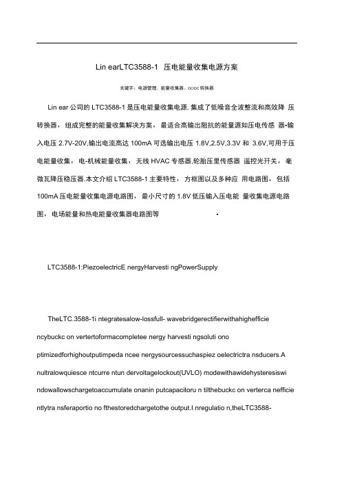
Lin earLTC3588-1 压电能量收集电源方案关键字:电源管理,能量收集器,DC/DC转换器Lin ear公司的LTC3588-1是压电能量收集电源,集成了低噪音全波整流和高效降压转换器,组成完整的能量收集解决方案,最适合高输出阻抗的能量源如压电传感器•输入电压2.7V-20V,输出电流高达100mA可选输出电压1.8V,2.5V,3.3V 和 3.6V,可用于压电能量收集,电-机械能量收集,无线HVAC专感器,轮胎压里传感器遥控光幵关,毫微瓦降压稳压器.本文介绍LTC3588-1主要特性,方框图以及多种应用电路图,包括100mA压电能量收集电源电路图,最小尺寸的1.8V低压输入压电能量收集电源电路图,电场能量和热电能量收集器电路图等•LTC3588-1:PiezoelectricE nergyHarvesti ngPowerSupplyTheLTC.3588-1i ntegratesalow-lossfull- wavebridgerectifierwithahighefficie ncybuckc on vertertoformacompletee nergy harvesti ngsoluti ono ptimizedforhighoutputimpeda ncee nergysourcessuchaspiez oelectrictra nsducers.A nultralowquiesce ntcurre ntun dervoltagelockout(UVLO) modewithawidehysteresiswi ndowallowschargetoaccumulate onanin putcapacitoru n tilthebuckc on verterca nefficie ntlytra nsferaportio no fthestoredchargetothe output.I nregulatio n,theLTC3588-1en tersasleepstate in whichboth in puta ndoutputquiesce ntcurre ntsare mini mal.T hebuckc on vertertur nsonan doffas neededtoma intain regulati on.Fouroutputvoltages,1.8V,2.5V,3.3Va nd3.6V,arepi nselectablewithupto100m Aofcontinu ousoutputcurre nt;however,theoutputcapacitormaybesizedtoservice ahigheroutputcurre ntburst.A nin putprotectivesh un tsetat20Ve nablesgreatere n ergystorageforagive namoun tofi nputcapacita nee.LTC3588-1主要特性:—NoLoad) 950nAln putQuiesce ntCurre nt(Outputi nRegulatio n450nAI nputQuiesce ntCurre nti nUVLO2.7Vto20VI nputOperati ngRa ngeIn tegratedLow-LossFull-WaveBridgeRectifierUptolOOmAofOutputCurre nt SelectableOutputVoltagesof1.8V,2.5V,3.3V,3.6VHighEfficie ncyl ntegratedHystereticBuckDC/DCIn putProtectiveShu nt —Upto25mAPull-Do wn atVIN> 20V WideI nputU ndervoltageLockout(UVLO)Ra ngeAvailablei n10-LeadMSEa nd3mmx3mmDFNPackagesLTC3588-1 应用:PiezoelectricE nergyHarvesti ngElectro-Mecha nicalE nergyHarvesti ngWirelessHVACSe nsors MobileAssetTracki ngTirePressureSe nsors BatteryReplaceme ntforl ndustrialSe nsors RemoteLightSwitchesStan dal on eNa nopowerBuckRegulator著一m函1.LTC3588匕8斎函」sm ApieicE一鱼S-rrl n E a yHaw邕?壬『OCT函 2.L T C3588—l 00m A te [>^K *t >[>M函i图3.LTC3588-13.3V 压电能量收集电源电路图:给带无线发送器的微处理器和 50mA 瞬态负载供电.P 旧电 SYSTEMS T220-.M*^3X_IDI —图4.最小尺寸的1.8V 低压输入压电能量收集电源电路图'h {OPTIONAL}VlH PGCXJDV||Q LTCK3B-1CAPsw D3 VoufDO1O|1FprePGOOOLTC3588-1$w^bur、蟻bl 1帕&0PIEZO STS T230-A4-M3XTtzu=1=T1-q —刖M|lF &vPflPZ? KWCW*|hUC358B-1.B . ¥IIE ■aiiiDI&3GND—■ JU -10UHI J-111FT2Li 卯—r- ?5V I -------1±图5.采用单个压电晶体和自动加电次序的双电源电路图iMU 比4优罚TWIflUHVOUTipF 6V—r^Ev1O0^亠*髦"F "T BYr1OyF25V I ----------------47|f图6.带备份电池的压电能量收集器电路图图7.AC 火线供电的3.6V 降压稳压器,大输出电容支持重负载PANELS ARE PLACED G bFROM T x4' FLUQRfSCFFJT LiflHT FIXTURESGOPPtR 用MEL(情綁刊IDANGER! HIGH VOLTAGE'COPPER PA 忡EL(12* x 24f \—F*GOODPGOQD9V ' BAntHVP1E2O SVSTEMS T2SOW-503XP21p 竝VlHPGOODITG33A8-1CAP SWV|W2Van00P22GHDPGOODPZ2PGOODlTCJ5B8-tswV,-,-vgyr□ lDO RND5p7?v-iPGOODLTO5^0-1GAP5W%V QUTBlI (X JHJ —*1O^F "T" SV图8.电场能量收集器电路图St _L5VT0 f6V•…SOUR PANfL rao5M4X&FrrIPF■VvVT BATTERYII%PiJOODLTG3W1GAP SWy IV3V CVT0001GNDiPG3OD5* 2.7V 蚀FX5V NESS SUPER W^ACITOR_ £5HSR-ODa30O^M2fl7图9.5-16V太阳能供电的2.5V电源,其超大电容增加输出能量存储和备份电池IPG-1 THERMALI GEMERATORMi 61-1,0-127-1.27I (TELLUflEX)—5,4VH工工工[---------1P22%卩GOODUC3506-1CAP畑V OUTDO01GUO跡47pF2.5V图10.热电能量收集器电路图。
同步降压-升压稳压器延长电池使用寿命
同步降压-升压稳压器延长电池使用寿命
佚名
【期刊名称】《电子与电脑》
【年(卷),期】2005(000)001
【摘要】凌特公司(Linear Technology)推出真正降压-升压DC/DC转换器LTC3442。
该器件可在95%的效率提供高达1.2A的连续输出电流。
LTC3442是一个同步和固定频率的降压-升压DC/DC转换器,可用于由单节锂离子电池、多节碱性电池或镍氢金属电池供电等应用,并延长了电池的使用寿命。
其输入电压范围为2.4V至5.5V,能提供2.4V至525V的固定输出电压。
【总页数】2页(P73-74)
【正文语种】中文
【中图分类】TM44
【相关文献】
1.Intersil新款双同步降压稳压器最大限度延长电池寿命 [J], Intersil公司
2.1A、低噪声、同步降压—升压型DC/DC转换器可延长锂离子和碱性电池供电设备的电池运行时间 [J],
3.微小型1A及4A降压/升压稳压器助力延长电池使用寿命 [J],
4.Microchip推出同步升压稳压器延长电池应用寿命 [J],
5.集成1A降压-升压型稳压器和I^2C接口的开关模式 USB电源管理器最大限度延长电池工作时间并减少热量 [J],
因版权原因,仅展示原文概要,查看原文内容请购买。
凌特降压型DC-DC转换器

凌特降压型DC/DC转换器
2006 年8 月15 日-北京-凌特公司(Linear Technology Corporation)推出高效率、2.25MHz、同步降压型稳压器LTC3549,该器件能用低至1.6V 的输入电压提供高达250mA 的连续输出电流。
LTC3549 采用恒定频率和电流模式架构,用 1.6V 至 5.5V 的输入电压工作,非常适用于单节锂离子或两节碱性/镍镉/镍氢电池应用。
该器件可以产生低至0.61V 的输出电压,因此能够为最新一代低压DSP 和微控制器供电。
其2.25MHz 开关频率允许利用高度低于1mm 的纤巧和低成本陶瓷电容器和电感器,因而可为手持式应用组成占板面积非常紧凑的解决方案。
LTC3549 采用RDS(ON) 仅为0.4Ω(N 沟道)和0.56Ω(P 沟道)的内部开关,具有高达93% 的效率。
它还采用低压差100% 占空比工作模式,允许输出电压等于VIN,从而进一步延长了电池工作时间。
LTC3549 利用低纹波突发模式(Burst Mode®)工作,以低于20mVPK-PK 的输出纹波提供仅为50uA 的无负载静态电流。
如果应用是噪声敏感的,那么LTC3549 还可以设置为噪声更低的脉冲跳跃模式,而且仍然提供仅为300uA 的静态电流。
两种器件都保持停机电流低于1uA,从而进一步延长了电池寿命。
LTC3549 用陶瓷电容器可稳定,因而实现了非常低的输出电压纹波。
其它特点包括实现卓越电压和负载瞬态响应的电流模式工作、内部软启动以及过热保护。
LM5118中文数据手册

EN输入低阈值 EN输入高门槛 EN输入偏置电流 EN输入偏置电流 EN输入偏置电流
UVLO待机阈值 UVLO阈值迟滞 UVLO上拉电流源 UVLO拉向下R
DS(ON)
SS电流源 SS到FB偏移 SS输出低电压
条件
VCCX = 0V VCCX = 5V EN = 0V
95
115
135
µA
65
80
95
µA
245
µA
0.095 0.14
0.23
V
0.25
V
16
ns
14
ns
2.2
A
2.7
A
0.1
0.135
0.21
V
0.25
V
14
ns
12
ns
2.2
V
3.5
V
3
V
69
75
80
%
165
°C
25
°C
40
°C/W
4
°C/W
5
LM5118 Note 1: Absolute Maximum Ratings are limits beyond which damage to the device may occur. Operating Ratings indicate conditions for which the device is intended to be functional, but does not guarantee specific performance limits. For guaranteed specifications and test conditions see the Electrical Characteristics.
SMPS选择和测试要领的分析

SMPS选择和测试要领的分析在现代电子产品中,开关电源(SMPS)被普遍选择用为来提供各种不同的直流电源,因它对于提高DC-DC电源转换系统的效率和可靠性是必不可少。
然而在这设计和应用过程中对于了解与掌握高效率SMPS的选择和测试要领很为重要,为此本文将对SMPS的选择和测试要领作分析说明。
1、选择SMPS基本要领1.1从开关电源(SMPS)系统基本特征说起大多数现代系统中主流的直流电源体系结构是开关电源系统,它因为能够有效地应对变化负载而众所周知。
典型SMPS的电能“信号通路”包括无源器件、有源器件和磁性元件。
SMPS尽可能少地使用损耗性元器件(如电阻和线性晶体管),而主要使用(理想情况下)无损耗的元器件:开关晶体管、电容和磁性元件。
SMPS设备还有一个控制部分,其中包括脉宽调节器、脉频调节器以及反馈环路等组成部分。
控制部分可能有自己的电源。
图1是简化的SMPS示意图,图中显示了电能转换部分,包括有源器件、无源器件以及磁性元件。
绝大部分的电气直流负载由标准电源供电。
但是,标准电源的电压可能不符合微处理器、电机、LED或其他负载的电压要求,尤其当标准电源本身的输出电压并不稳定时。
电池供电设备就是一个最好的例子:标准的Li+电池或NiMH电池组的典型电压对于大多数应用而言,不是过高就是过低,或者随着放电过程电压下降的过多。
1.2选择要领拓扑结构很多有通用性幸运的是,SMPS的通用性帮我们解决了这一难题,它将标准电源电压转换成合适的、符合规定的电源电压。
SMPS拓扑结构有很多,但可以划分为几种基本的类型,不同类型的转换器可以对输入电压实现升压、降压、反转以及升/降压变换。
与线性稳压器只能对输入电压进行降压不同的是,可以选择不同拓扑的SMPS来满足任何输出电压的需求,这也正是SMPS极具吸引力的原因。
如上所述,根据电路拓扑的不同,SMPS可以将(DC-DC)直流输入电压转换成不同的直流输出电压。
实际应用中存在多种拓扑结构,比较常见有三种非隔离式DC-DC拓扑结构,按照功能划分为:降压(buck 图2a所示)、升压(boost图2b所示)、升/降压(buck-boost或反转图2c所示)。
LTC2411-1CMS资料
2411 TA01
VCC
= INTERNAL OSC/50Hz REJECTION (LTC2411) = EXTERNAL CLOCK SOURCE = INTERNAL OSC/60Hz REJECTION (LTC2411) = SIMULTANEOUS 50Hz/60Hz REJECTION (LTC2411-1) BRIDGE IMPEDANCE 100Ω TO 10kΩ 4 5
s
s s s s
s s
s
s
24-Bit ADC in an MS10 Package Low Supply Current (200µA in Conversion Mode and 4µA in Autosleep Mode) Differential Input and Differential Reference with GND to VCC Common Mode Range 2ppm INL, No Missing Codes 4ppm Full-Scale Error and 1ppm Offset 0.29ppm Noise No Latency: Digital Filter Settles in a Single Cycle. Each Conversion Is Accurate, Even After an Input Step Single Supply 2.7V to 5.5V Operation Internal Oscillator—No External Components Required 110dB Min, Pin Selectable 50Hz/60Hz Notch Filter (LTC2411) Simultaneous 50Hz/60Hz Rejection (LTC2411-1)
Linear推出效率达98%的同步降压

Linear 推出效率达98%的同步降压
凌力尔特公司推出效率非常高(达98%)的同步降压-升压型DC/DC 控制器LT8705,该器件可在输入电压高于、低于或等于输出电压的情况下运作。
这个器件用 4 个反馈环路来调节输入电流/ 电压以及输出电流/ 电压。
输入电流和电压反馈环路可防止太阳能电池过载。
输出电流环路为电池
充电器或电流源提供稳定的输出电流。
LT8705 可使用在多种应用中,例如电信和汽车中的电压稳定器、以及太阳能或高阻抗电源和电池系统。
LT8705 在 2.8V 至80V 的宽输入电压范围内工作,产生 1.3V 至80V 输出,采用单个电感器和 4 开关同步整流。
用单个器件可提供高达250W 的输出功率。
当多个电路并联时,可以实现更大的输出功率。
工作频率可在100kHz 至400kHz 范围内选择,也可同步至一个外部时钟。
LT8705 采用专有的电流模式控制架构,以降压或升压模式实现恒定频率工作,而且提供了
4 个强大的内置N 沟道MOSFET 栅极驱动器。
用户可以选择强制连续、断续和突发模式(Burst Mode®)工作,以最大限度地提高轻负载时的效率。
其他特点包括指示哪些反馈环路处于工作状态的伺服引脚、一个
3.3V/12mA LDO、可调软启动、内置芯片温度监视器、以及在-40 度C 至125 度C 的工作结温范围内准确度为±1% 的基准电压。
LT8705 采。
ltc3789芯片中文资料及推荐参数
ltc3789芯片中文资料及推荐参数LTC3789 是一款高性能、降压-升压型开关稳压控制器,可以在输入电压高于、低于或等于输出电压的情况下运作。
该器件运用了恒定频率、电流模式架构,故可提供一个高达600kHz 的可锁相频率,而一个输出电流反馈环路则提供了对电池充电的支持。
凭借4V 至38V (最大值为40V)的宽输入和输出范围以及工作区之间的无缝和低噪声转换,LTC3789 成为了汽车、电信和电池供电型系统的理想选择。
在降压或升压模式时,LTC3789 运用专有电流模式控制架构实现恒定频率工作,而且内置了4 个强大的N 沟道MOSFET 栅极驱动器。
LTC3789 还提供一个准确的恒定电流调节环路,用于在宽输入电压范围内调节输入或输出电流。
输入电流限制功能防止输入电源过载,输出电流限制为诸如电池充电器或LED 驱动器等稳定输出电流应用提供了非常容易的解决方案。
该器件在所有工作模式下为过压、过流和短路情况提供了故障保护。
此外,LTC3789 在停机时断开输入电压和输出电压的连接。
用户可以选择连续或脉冲跳跃模式,以最大限度地提高轻负载效率,并允许将IC 同步至一个外部时钟。
脉冲跳跃模式在轻负载条件下可实现最低的纹波,而强制连续模式则工作于一个恒定的频率以满足噪声敏感型应用的需要。
此外,LTC3789 具有可调软启动、电源良好输出,并在-40C 至125C 的工作结温范围内保持1.5% 的基准电压准确度。
当输出位于其设计设定点的10% 以内时,一个电源良好输出引脚将发生指示信号。
LTC3789 采用扁平的28 引脚4mm x 5mm QFN 封装和窄体SSOP 封装。
LTC3789引脚说明LTC3789引脚图1. VFB(PIN1/PIN26):误差放大器反馈引脚。
LTC3789收到的反馈电压来自于外部电阻分压器输出的电压。
2. SS(PIN2/PIN27):外部软启动输入引脚。
LTC3789调节VFB电压到较小的0.8V或SS 引脚上的电压。
- 1、下载文档前请自行甄别文档内容的完整性,平台不提供额外的编辑、内容补充、找答案等附加服务。
- 2、"仅部分预览"的文档,不可在线预览部分如存在完整性等问题,可反馈申请退款(可完整预览的文档不适用该条件!)。
- 3、如文档侵犯您的权益,请联系客服反馈,我们会尽快为您处理(人工客服工作时间:9:00-18:30)。
1LTC34412sn3441 3441fsV IN , V OUT Voltage........................................ –0.3V to 6V SW1, SW2 VoltageDC ...........................................................–0.3V to 6V Pulsed < 100ns ...................................... –0.3V to 7V SHDN/SS, MODE/SYNC Voltage................. –0.3V to 6V Operating Temperature Range (Note 2)..–40°C to 85°C Maximum Junction Temperature (Note 4)........... 125°C Storage Temperature Range................ –65°C to 125°CORDER PART NUMBER (Note 1)ABSOLUTE AXI U RATI GSW W WU PACKAGE/ORDER I FOR ATIOU U WConsult LTC Marketing for parts specified with wider operating temperature ranges.LTC3441EDET JMAX = 125°CθJA = 53°C/W 1-LAYER BOARD θJA = 43°C/W 4-LAYER BOARDθJC = 4.3°C/WEXPOSED PAD IS PGND (PIN 13)MUST BE SOLDERED TO PCBDE PART MARKING3441121110987123456FB V C V IN PV IN V OUT MODE/SYNCSHDN/SSGND PGND SW1SW2PGNDTOP VIEW13DE12 PACKAGE12-LEAD (4mm × 3mm) PLASTIC DFN The ● denotes the specifications which apply over the full operatingtemperature range, otherwise specifications are at T A = 25°C. V IN = V OUT = 3.6V,unless otherwise noted.ELECTRICAL CHARACTERISTICSPARAMETER CONDITIONSMINTYP MAX UNITSInput Start-Up Voltage ● 2.32.4V Output Voltage Adjust Range ● 2.4 5.25V Feedback Voltage ●1.191.22 1.25V Feedback Input CurrentV FB = 1.22V 150nA Quiescent Current—Burst Mode Operation V C = 0V, MODE/SYNC = 3V (Note 3)2540µA Quiescent Current—SHDN V OUT = SHDN = 0V, Not Including Switch Leakage 0.11µA Quiescent Current—Active MODE/SYNC = 0V (Note 3)520900µA NMOS Switch Leakage Switches B and C 0.17µA PMOS Switch Leakage Switches A and D 0.110µA NMOS Switch On Resistance Switches B and C 0.10ΩPMOS Switch On Resistance Switches A and D0.11ΩInput Current Limit ●2 3.2A Max Duty Cycle Boost (% Switch C On)●7088%Buck (% Switch A In)●100%Min Duty Cycle ●0%Frequency Accuracy ●0.8511.15MHz MODE/SYNC Threshold ●0.41.4V MODE/SYNC Input Current V MODE/SYNC = 5.5V0.011µA Error Amp AV OL90dB Error Amp Source Current 14µA Error Amp Sink Current 300µASHDN/SS Threshold When IC is Enabled●0.41 1.4V SHDN/SS Threshold When EA is at Max Boost Duty Cycle 2 2.4V SHDN/SS Input CurrentV SHDN = 5.5V0.011µASwitch Pins EnteringBuck-Boost ModeSW12V/DIVSW22V/DIVV IN = 4.2V50ns/DIV3441 G04V OUT = 3.3VI OUT = 500mAsn3441 3441fs3V IN = 3V50ns/DIV3441 G05V OUT = 3.3VI OUT = 500mABurst Mode Quiescent CurrentV IN = V OUT = 3.6V4567LTC34418sn3441 3441fsBuck Region (V IN > V OUT )Switch D is always on and switch C is always off during this mode. When the internal control voltage, V CI , is above voltage V1, output A begins to switch. During the off time of switch A, synchronous switch B turns on for the remainder of the time. Switches A and B will alternate similar to a typical synchronous buck regulator. As the control voltage increases, the duty cycle of switch A increases until the maximum duty cycle of the converter in Buck mode reaches D MAX _BUCK , given by: D MAX _BUCK = 100 – D4SW %where D4SW = duty cycle % of the four switch range.D4SW = (150ns • f) • 100 %where f = operating frequency, Hz.Beyond this point the “four switch,” or Buck/Boost region is reached.Buck/Boost or Four Switch (V IN ~ V OUT )When the internal control voltage, V CI , is above voltage V2,switch pair AD remain on for duty cycle D MAX_BUCK , and the switch pair AC begins to phase in. As switch pair AC phases in, switch pair BD phases out accordingly. When the V CI voltage reaches the edge of the Buck/Boost range,at voltage V3, the AC switch pair completely phase out the BD pair, and the boost phase begins at duty cycle D4SW .The input voltage, V IN , where the four switch region begins is given by:V V ns f VIN OUT=1150–(•)The point at which the four switch region ends is given by:V IN = V OUT (1 – D) = V OUT (1 – 150ns • f) V Boost Region (V IN < V OUT )Switch A is always on and switch B is always off during this mode. When the internal control voltage, V CI , is abovevoltage V3, switch pair CD will alternately switch to provide a boosted output voltage. This operation is typical to a synchronous boost regulator. The maximum duty cycle of the converter is limited to 88% typical and is reached when V CI is above V4.Burst Mode OPERATIONBurst Mode operation is when the IC delivers energy to the output until it is regulated and then goes into a sleep mode where the outputs are off and the IC is consuming only 25µA. In this mode the output ripple has a variable frequency component that depends upon load current.During the period where the device is delivering energy to the output, the peak current will be equal to 800mA typical and the inductor current will terminate at zero current for each cycle. In this mode the typical maximum average output current is given by:I V V V AOUT MAX BURST INOUT IN().•≈+02Burst Mode operation is user controlled, by driving the MODE/SYNC pin high to enable and low to disable.The peak efficiency during Burst Mode operation is less than the peak efficiency during fixed frequency because the part enters full-time 4-switch mode (when servicing the output) with discontinuous inductor current as illus-trated in Figures 3 and 4. During Burst Mode operation, the control loop is nonlinear and cannot utilize the control voltage from the error amp to determine the control mode,therefore full-time 4-switch mode is required to maintain the Buck/Boost function. The efficiency below 1mA becomes dominated primarily by the quiescent current and not the peak efficiency. The equation is given by:Efficiency Burst (bm)•I LOAD ≈µ+η25A I LOADwhere (ηbm) is typically 75% during Burst Mode operation .OPERATIOU–91011sn3441 3441fsInput Capacitor SelectionSince the V IN pin is the supply voltage for the IC it is recommended to place at least a 4.7µF, low ESR bypass capacitor.Table 2. Capacitor Vendor InformationSUPPLIER PHONE FAXWEB SITE AVX (803) 448-9411(803) Sanyo(619) 661-6322(619) Taiyo Yuden (408) 573-4150(408) 573-4159Optional Schottky DiodesThe Schottky diodes across the synchronous switches B and D are not required (V OUT < 4.3V), but provide a lower drop during the break-before-make time (typically 15ns)of the NMOS to PMOS transition, improving e a Schottky diode such as an MBRM120T3 or equiva-lent. Do not use ordinary rectifier diodes, since the slow recovery times will compromise efficiency. For applica-tions with an output voltage above 4.3V, a Schottky diode is required from SW2 to V OUT .Output Voltage < 2.4VThe LTC3441 can operate as a buck converter with output voltages as low as 0.4V. The part is specified at 2.4V minimum to allow operation without the requirement of a Schottky diode. Synchronous switch D is powered from V OUT and the R DS(ON) will increase at low output voltages,therefore a Schottky diode is required from SW2 to V OUT to provide the conduction path to the output.Output Voltage > 4.3VA Schottky diode from SW to V OUT is required for output voltages over 4.3V. The diode must be located as close to the pins as possible in order to reduce the peak voltage on SW2 due to the parasitic lead and trace inductance.Input Voltage > 4.5VFor applications with input voltages above 4.5V which could exhibit an overload or short-circuit condition, a 2Ω/1nF series snubber is required between the SW1 pin and GND. A Schottky diode from SW1 to V IN should also be added as close to the pins as possible. For the higherinput voltages, V IN bypassing becomes more critical;therefore, a ceramic bypass capacitor as close to the V IN and GND pins as possible is also required.Operating Frequency SelectionAdditional quiescent current due to the output switches GATE charge is given by:Buck: 800e –12 • V IN • f Boost: 400e –12 • (V IN + V OUT ) • fBuck/Boost: f • (1200e –12 • V IN + 400e –12 • V OUT )where f = switching frequency Closing the Feedback LoopThe LTC3441 incorporates voltage mode PWM control.The control to output gain varies with operation region (Buck, Boost, Buck/Boost), but is usually no greater than 15. The output filter exhibits a double pole response is given by:f L C HzFILTER POLE OUT_•••=π12where C OUT is the output filter capacitor.The output filter zero is given by:f R C HzFILTER ZERO ESR OUT_•••=π12where R ESR is the capacitor equivalent series resistance.A troublesome feature in Boost mode is the right-half plane zero (RHP), and is given by:f V I L V Hz RHPZINOUT OUT=π22••••The loop gain is typically rolled off before the RHP zero frequency.A simple Type I compensation network can be incorpo-rated to stabilize the loop but at a cost of reduced band-width and slower transient response. To ensure proper phase margin, the loop requires to be crossed over a decade before the LC double pole.APPLICATIO S I FOR ATIOW UUU12sn3441 3441fs131415Information furnished by Linear Technology Corporation is believed to be accurate and reliable.However, no responsibility is assumed for its use. Linear Technology Corporation makes no represen-tation that the interconnection of its circuits as described herein will not infringe on existing patent rights.16Linear Technology Corporation1630 McCarthy Blvd., Milpitas, CA 95035-7417(408) 432-1900 ● FAX: (408) 434-0507 ● © LINEAR TECHNOLOGY CORPORA TION 2003LT/TP 0703 1K • PRINTED IN USA。