2A双向直流电机(马达)驱动芯片 RZ7888
LMD18200T直流电机驱动板使用说明
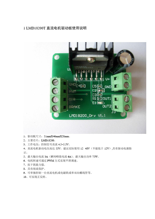
1 LMD18200T直流电机驱动板使用说明
1、驱动板尺寸:51mmX46mmX28mm。
2、主要芯片:LMD18200。
3、工作电压:控制信号直流4.5~5.5V。
4、直流电机驱动电压高达55V,建议实际使用12--48V(不能低于12V),具有驱动电源指示。
5、最大输出电流3A(瞬间峰值电流6A),最大输出功率75W。
6、电机转速可通过PWM方式实现平滑调速。
7、抗干扰能力强。
8、具有续流保护。
9、可单独控制一台直流电机或电磁铁或单双向螺线管等。
10、可实现正反转。
2 接口说明
注意:电源和地不要接反,以免损坏器件。
3 主要芯片介绍
LMD18200是美国国家半导体公司(NS)推出的专用于直流电动机驱动的H桥组件。
同一芯片上集成有CMOS控制电路和DMOS功率器件,利用它可以与主处理器、电机和增量型编码器构成一个完整的运动控制系统。
LMD18200广泛应用于打印机、机器人和各种自动化控制领域。
1、主要性能
峰值输出电流高达6A,连续输出电流达3A;
工作电压高达55V;
Low RDS(ON) typically 0.3W per switch;
TTL/CMOS兼容电平的输入;
无“shoot-through”电流;
具有温度报警和过热与短路保护功能;
结温达170℃时,芯片关断;
具有良好的抗干扰性。
2、典型应用
驱动直流电机
伺服机构系统位置与转速
应用于机器人控制系统
应用于数字控制系统
应用于电脑打印机与绘图仪3、LMD18200逻辑真值表。
IAD3988中文 A3988 马达驱动IC
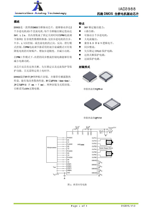
D 3988 四路DMOS 全桥电机驱动芯片图1. 典型应用电路描述D3988是一款四路DMOS全桥驱动芯片,能够驱动多达2个步进电机或4个直流电机。
每个全桥输出额定值高达36V, 1.2 A。
其内部集成了固定关闭时间的PWM电流调节器和2 位非线性数模转换器,支持步进电机的全步、半步、1/4步控制,或直流电机的正向、反向、滑行模式控制。
其PWM电流调节器采用的混合衰减模式可有效降低电机的可闻噪声,增加步进精度,并减小功耗。
在PWM工作模式下,内置的同步整流控制电路能够有效减小电路功耗。
该芯片还具有过热关断、欠压锁定以及过流保护等保护功能,且无需特定的上电时序。
D3988提供EV和JP两种贴片封装,并都带有裸露散热焊盘,能有效改善散热性能。
EV是QFN36(6mm ×6mm),JP是TQFP48 (7 mm × 7 mm)。
两种封装为无铅封装,引框采用100%无锡电镀。
特点● 36V 额定输出能力; ● 4路全桥; ● 可驱动2个步进电机; ● 大电流输出; ● 兼容3.3 和5 V 逻辑电平; ● 同步整流; ● 欠压锁定(UVLO)保护电路; ● 过热关断保护电路;● 过流保护电路。
封装形式 带散热盘的TQFP48 带散热盘的QFN36 IAD订购信息Part Number Package Packing IAD3988PQT 48 pin TQFP with exposed thermal pad 2500 pieces per trayIAD3988SQTR 36 pin QFN with exposed thermal pad 3000 pieces per reel引脚排列图QFN36LQFP48引脚列表QFN36 LQFP48 Pin Name Pin Description2 3 OUT1A DMOS Full-Bridge 1 Output A3 4 SENSE1 Sense Resistor Terminal for Bridge 14 5 OUT1B DMOS Full-Bridge 1 Output B5 6 VBB1 Load Supply Voltage6 8 OUT2B DMOS Full-Bridge 2 Output B7 9 SENSE2 Sense Resistor Terminal for Bridge 28 10 OUT2A DMOS Full-Bridge 2 Output A9 13 PHASE4ControlInput10 14 PHASE3 Control Input11 15 VDD Logic Supply Voltage12 16 VREF1AnalogInput 13 17 VREF2AnalogInput 14 18 VREF3AnalogInput 15 19 VREF4AnalogInput16 20 GND Ground17 21 PHASE2 Control Input18 22 PHASE1ControlInput19 24 I14 Control Input20 27 OUT4A DMOS Full-Bridge 4 Output A21 28 SENSE4 Sense Resistor Terminal for Bridge 422 29 OUT4B DMOS Full-Bridge 4 Output B23 31 VBB2 Load Supply Voltage24 32 OUT3B DMOS Full-Bridge 3 Output B25 33 SENSE3 Sense Resistor Terminal for Bridge 326 34 OUT3A DMOS Full-Bridge 3 Output A27 37 I13 Control Input28 38 I12 Control Input29 39 I11 Control Input30 40 GND Ground31 42 VCP Reservoir Capacitor Terminal32 43 CP1 Charge Pump Capacitor Terminal33 44 CP2 Charge Pump Capacitor Terminal34 45 I01 Control Input35 46 I02 Control Input36 47 I03 Control Input1 48 I04 Control Input1, 2, 7, 11, 12, 23, 25, 26, 30,35, 36, 41NC No ConnectPAD Exposed pad for enhanced thermal perfor-mance. Should be soldered to the PCB.。
丹东华奥电子 LD33035 无刷直流电机控制器说明书
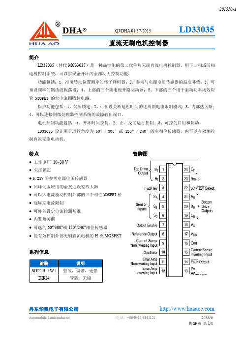
丹东华奥电子有限公司简介LD33035(替代MC33035)是一种高性能的第二代单片无刷直流电机控制器。
用于三相或四相电机控制系统,可以实现全开环的全部动力控制功能。
功能包括:1、准确转动位置测序的转子译码器;2、参考与电源电压传感器的温度补偿;3、可预设频率的锯齿波振荡器;4、上部的三个集电极开路驱动器;5、下部的三个用于驱动功率场效应管MOSFET 的大电流图腾柱电路。
保护功能包括:1、欠压锁定;2、可预设关断延迟时间的逐周期电流限制模式;3、内部热关断;4、可以连接到微处理器控制系统的故障输出端口。
电机控制功能包括:1、开环时间控制;2、正、反向运行控制;3、可控的启用和制动。
LD33035设计用于运行角度为60°/300°或120°/240°的电相位传感器,也可以有效地控制直流无刷电动机。
特点管脚图●工作电压10~30V ●欠压锁定●6.25V 的参考电源电压传感器●闭环伺服应用的全接近误差放大器●可以大电流驱动控制外部的三个相位MOSFET 桥●逐周期电流限制●可外部设定电流检测基准●内置热关断●可选的60°/300°或120°/240°相位传感器●能有效控制外部无刷直流电机的H 桥MOSFET系列信息封装说明SOP24L (W )管装,编带,无铅DIP24管装,无铅直流无刷电机控制器管脚功能描述丹东华奥电子有限公司功能示意图丹东华奥电子有限公司极限参数丹东华奥电子有限公司电参数(V CC=V C=20V,R T=4.7k,C T=10nF,T A=25℃,除非另外说明)丹东华奥电子有限公司CC C T T A注:1、输入共模电压或输入信号电压不应超过-0.3V。
2、调节电压不得超过−0.3至V REF范围。
丹东华奥电子有限公司介绍LD33035(替代MC33035)是一种单片的直流无刷电机控制器,它包含了开环控制的三、四相电机控制系统所需的全部功能。
MC-7882-AZ资料
Caution Observe precautions when handling because these devices are sensitive to electrostatic discharge.GaAs MULTI-CHIP MODULEMC-7882870 MHz CATV 20 dB POWER DOUBLER AMPLIFIERDESCRIPTIONThe MC-7882 is a GaAs Multi-chip Module designed for use in CATV applications up to 870 MHz. This unit has low distortion, low noise figure and return loss across the entire frequency band.Reliability and performance uniformity are assured by our stringent quality and control procedures.FEATURES• Low distortion • High linear gain G L = 20.0 dB MIN. @ f = 870 MHz• Low return loss<R>ORDERING INFORMATIONPart Number Order Number PackageSupplying FormMC-7882MC-7882-AZ7-pin special with heatsink (Pb-Free)25 pcs MAX./TrayRemark To order evaluation samples, contact your nearby sales office.Part number for sample order: MC-7882ABSOLUTE MAXIMUM RATINGS (T A = +25°C)Parameter Symbol Ratings UnitSupply Voltage V DD 30 V Input VoltageNoteV i 65.0 dBmV Operating Case Temperature T C −30 to +100 °C Storage TemperatureT stg−40 to +100°CNote In case of single toneThe mark <R> shows major revised points.The revised points can be easily searched by copying an "<R>" in the PDF file and specifying it in the "Find what:" field.Document No. PG10314EJ02V0DS (2nd edition) Date Published December 2006 NS CP(N)2002, 2006RECOMMENDED OPERATING CONDITIONS (Z S = Z L = 75 Ω)UnitTYP.MAX.Conditions MIN.Parameter Symbol TestSupply Voltage V DD23.5 24.0 24.5 VInput Voltage V i110 channel,−34.0 37.0 dBmV10 dB tilted across the bandOperating Case Temperature T C−30 +25 +85 °C ELECTRICAL CHARACTERISTICS (T C = 30±5°C, V DD = 24 V, Z S = Z L = 75 Ω)MAX.UnitConditions MIN.TYP.Parameter Symbol TestLinear Gain G L f = 870 MHz 20.0 −21.0 dBGain Slope G Slope f = 40 to 870 MHz 0.4 0.8 1.2 dBGain Flatness G Flatness f = 40 to 870 MHz, Peak to valley −−0.6 dBNoise Figure 1 NF1 f = 50 MHz −− 6.0 dBNoise Figure 2 NF2 f = 870 MHz −− 6.5 dBOFF 310 −360 mA Operating Current I DD RFComposite Triple Beat CTB 110 channel, −−−60 dBcCross Modulation XM V O = 52 dBmV at 745.25 MHz, −−−55 dBc Composite 2nd Order Beat CSO 10 dB tilted across the band −−−63 dBcInput Return Loss 1 RLi1 f = 40 to 160 MHz 20 −−dBInput Return Loss 2 RLi2 f = 160 to 320 MHz 19 −−dBInput Return Loss 3 RLi3 f = 320 to 640 MHz 17.5 −−dBInput Return Loss 4 RLi4 f = 640 to 870 MHz 16 −−dBOutput Return Loss 1 RLo1 f = 40 to 160 MHz 20 −−dBOutput Return Loss 2 RLo2 f = 160 to 320 MHz 19 −−dBOutput Return Loss 3 RLo3 f = 320 to 640 MHz 17.5 −−dBOutput Return Loss 4 RLo4 f = 640 to 870 MHz 16 −−dB2Data Sheet PG10314EJ02V0DSPACKAGE DIMENSIONS7-PIN SPECIAL WITH HEATSINK (UNIT: mm)PIN CONNECTIONNOTES ON CORRECT USE(1) The space between PC board and root of the lead should be kept more than 1 mm to prevent undesired stressto the lead and also should be kept less than 4 mm to prevent undesired parasitic inductance.Recommended that space is 2.0 to 3.0 mm typical.(2) Recommended torque strength of the screw is 59 to 78 Ncm.(3) Form the ground pattern as wide as possible to minimize ground impedance.(to prevent undesired oscillation)All the ground pins must be connected together with wide ground pattern to decrease impedance difference.RECOMMENDED SOLDERING CONDITIONSThis product should be soldered and mounted under the following recommended conditions. For soldering methods and conditions other than those recommended below, contact your nearby sales office.Soldering Method Soldering Conditions Recommended Condition Symbol Partial Heating Peak temperature (pin temperature) : 350°C or below Note−Soldering time (per pin of device) : 3 seconds or lessNote The point of pin part heating must be kept more than 1.2 mm distance from the root of lead.4Data Sheet PG10314EJ02V0DSThe information in this document is current as of December, 2006. The information is subject to change without notice. For actual design-in, refer to the latest publications of NEC Electronics data sheets or data books, etc., for the most up-to-date specifications of NEC Electronics products. Not all products and/or types are available in every country. Please check with an NEC Electronics sales representative for availability and additional information.No part of this document may be copied or reproduced in any form or by any means without the prior written consent of NEC Electronics. NEC Electronics assumes no responsibility for any errors that may appear in this document.NEC Electronics does not assume any liability for infringement of patents, copyrights or other intellectual property rights of third parties by or arising from the use of NEC Electronics products listed in this document or any other liability arising from the use of such products. No license, express, implied or otherwise, is granted under any patents, copyrights or other intellectual property rights of NEC Electronics or others.Descriptions of circuits, software and other related information in this document are provided for illustrative purposes in semiconductor product operation and application examples. The incorporation of these circuits, software and information in the design of a customer's equipment shall be done under the full responsibility of the customer. NEC Electronics assumes no responsibility for any losses incurred by customers or third parties arising from the use of these circuits, software and information.While NEC Electronics endeavors to enhance the quality, reliability and safety of NEC Electronics products, customers agree and acknowledge that the possibility of defects thereof cannot be eliminated entirely. To minimize risks of damage to property or injury (including death) to persons arising from defects in NEC Electronics products, customers must incorporate sufficient safety measures in their design, such as redundancy, fire-containment and anti-failure features.NEC Electronics products are classified into the following three quality grades: "Standard", "Special" and "Specific".The "Specific" quality grade applies only to NEC Electronics products developed based on a customer-designated "quality assurance program" for a specific application. The recommended applications of an NEC Electronics product depend on its quality grade, as indicated below. Customers must check the quality grade of each NEC Electronics product before using it in a particular application.The quality grade of NEC Electronics products is "Standard" unless otherwise expressly specified in NEC Electronics data sheets or data books, etc. If customers wish to use NEC Electronics products in applications not intended by NEC Electronics, they must contact an NEC Electronics sales representative in advance to determine NEC Electronics' willingness to support a given application.(Note)••••••M8E 02. 11-1(1)(2)"NEC Electronics" as used in this statement means NEC Electronics Corporation and also includes itsmajority-owned subsidiaries."NEC Electronics products" means any product developed or manufactured by or for NEC Electronics (asdefined above).Computers, office equipment, communications equipment, test and measurement equipment, audioand visual equipment, home electronic appliances, machine tools, personal electronic equipment and industrial robots.Transportation equipment (automobiles, trains, ships, etc.), traffic control systems, anti-disastersystems, anti-crime systems, safety equipment and medical equipment (not specifically designed for life support).Aircraft, aerospace equipment, submersible repeaters, nuclear reactor control systems, lifesupport systems and medical equipment for life support, etc."Standard":"Special":"Specific":Data Sheet PG10314EJ02V0DS54590 Patrick Henry DriveSanta Clara, CA 95054-1817Telephone: (408) 919-2500Facsimile: (408) 988-0279Subject: Compliance with EU DirectivesCEL certifies, to its knowledge, that semiconductor and laser products detailed below are compliant with the requirements of European Union (EU) Directive 2002/95/EC Restriction on Use of Hazardous Substances in electrical and electronic equipment (RoHS) and the requirements of EU Directive 2003/11/EC Restriction on Penta and Octa BDE.CEL Pb-free products have the same base part number with a suffix added. The suffix –A indicates that the device is Pb-free. The –AZ suffix is used to designate devices containing Pb which are exempted from the requirement of RoHS directive (*). In all cases the devices have Pb-free terminals. All devices with these suffixes meet the requirements of the RoHS directive.This status is based on CEL’s understanding of the EU Directives and knowledge of the materials that go into its products as of the date of disclosure of this information.Restricted Substanceper RoHS Concentration Limit per RoHS(values are not yet fixed)Concentration containedin CEL devices-A -AZLead (Pb) < 1000 PPMNot Detected (*) Mercury < 1000 PPM Not DetectedCadmium < 100 PPM Not Detected Hexavalent Chromium < 1000 PPM Not DetectedPBB < 1000 PPM Not DetectedPBDE < 1000 PPM Not DetectedIf you should have any additional questions regarding our devices and compliance to environmental standards, please do not hesitate to contact your local representative.Important Information and Disclaimer: Information provided by CEL on its website or in other communications concerting the substance content of its products represents knowledge and belief as of the date that it is provided. CEL bases its knowledge and belief on information provided by third parties and makes no representation or warranty as to the accuracy of such information. Efforts are underway to better integrate information from third parties. CEL has taken and continues to take reasonable steps to provide representative and accurate information but may not have conducted destructive testing or chemical analysis on incoming materials and chemicals. CEL and CEL suppliers consider certain information to be proprietary, and thus CAS numbers and other limited information may not be available for release.In no event shall CEL’s liability arising out of such information exceed the total purchase price of the CEL part(s) at issue sold by CEL to customer on an annual basis.See CEL Terms and Conditions for additional clarification of warranties and liability.。
rz7886电路原理

rz7886电路原理rz7886电路原理是一种常见的电路设计,其主要功能是实现信号放大和滤波。
本文将详细介绍rz7886电路的原理、组成以及工作原理。
一、rz7886电路的原理rz7886电路是一种集成电路,主要由放大器、滤波器和输出级组成。
其中,放大器负责对输入信号进行放大,滤波器用于滤除杂散信号,而输出级则将处理后的信号输出。
二、rz7886电路的组成rz7886电路的主要组成部分包括电源、放大器、滤波器和输出级。
电源提供电路所需的电力,放大器负责对输入信号进行放大,滤波器用于滤除杂散信号,而输出级则将处理后的信号输出。
1. 电源:rz7886电路需要一个稳定的电源来提供所需的电力。
通常,电源会提供正负两种极性的电压,以满足不同的工作要求。
2. 放大器:rz7886电路中的放大器起到信号放大的作用。
放大器一般由多个晶体管或运算放大器组成,通过放大输入信号的幅度,使其能够满足后续电路的要求。
3. 滤波器:rz7886电路中的滤波器主要用于滤除输入信号中的杂散信号。
滤波器可以根据需要选择不同的类型,如低通滤波器、高通滤波器或带通滤波器等。
4. 输出级:rz7886电路的输出级负责将处理后的信号输出。
输出级通常由电阻、电容或功率放大器等组成,以满足电路输出的要求。
三、rz7886电路的工作原理rz7886电路的工作原理是通过依次经过放大器、滤波器和输出级的处理,将输入信号进行放大和滤波,并最终输出符合要求的信号。
1. 输入信号经过放大器放大:输入信号首先经过放大器,放大器会将输入信号的幅度放大到所需的程度。
放大器可以根据需要选择不同的放大倍数,以满足信号放大的要求。
2. 信号滤波:放大后的信号经过滤波器进行滤波处理。
滤波器可以滤除输入信号中的高频噪声或低频杂散信号,以使输出信号更加纯净和稳定。
3. 输出信号输出:经过放大和滤波后,信号进入输出级,输出级将处理后的信号输出到外部电路或设备中。
输出级可以根据需要选择不同的输出方式,如电压输出或电流输出等。
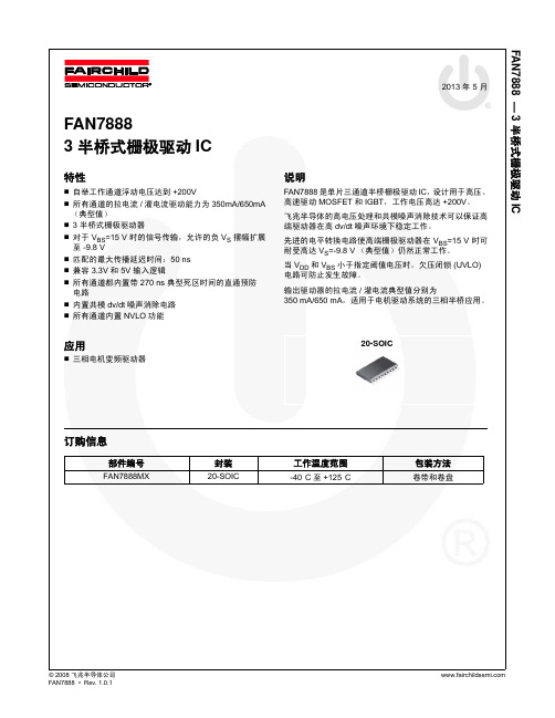
FAN7888
符号 VB1,2,3 VS1,2,3
VDD VHO1,2,3 VLO1,2,3
VIN TA
参数 高端浮动电源电压 高端浮动电源偏置电压 电源电压 高端输出电压 低端输出电压 逻辑输入电压 (HIN1,2,3 和 LIN1,2,3) 环境温度
最小值 VS1,2,3+10
6-VDD 10
VS1,2,3 GND GND -40
FAN7888 — 3 半桥式栅极驱动 IC
典型特性
t [ns]
ON
250 200
150 100
50
0 -40 -20
0 20 40 60 80 100 120 Temperature [°C]
图 4. 导通传播延时 vs 温度
t [ns]
OFF
300
250
200
150
100
50
0 -40 -20
至 -9.8 V 匹配的最大传播延迟时间:50 ns 兼容 3.3V 和 5V 输入逻辑 所有通道都内置带 270 ns 典型死区时间的直通预防
电路 内置共模 dv/dt 噪声消除电路 所有通道内置 NVLO 功能
说明
FAN7888 是单片三通道半桥栅极驱动 IC,设计用于高压、 高速驱动 MOSFET 和 IGBT,工作电压高达 +200V。
VIN=5 V VIN=0 V
500 650
mA
-9.8 -7.0 V
2.5
V
1.0 V
25
50 µA
2.0 µA
100 200 300 KΩ
注意:
4. 参数由设计者提供
© 2008 飞兆半导体公司
FAN7888 • Rev.1.0.1
马达驱动芯片大全
不可调
0.8欧 160度
0.4欧 150度 有
1欧 有 有
1.5欧 有 没有 没有 没有
有 有 有 有
AHX2021限流控制的优势 1)与其他玩具马达驱动IC比较,达到限制电流后,能够保持恒流输出,保护芯 片和马达不会烧毁,同时电流恒定,使马达维持充沛的动力。 2)限流可以调节,能够满足多种马达的限流要求。 3)在驱动转向马达的情况下,堵转达到限流后,堵转电流不随电源电压变化, 更省电。通过调整限流电阻,很容易匹配各种马达和电池。 4) 在恒流情况下,可进调整PWM频率,从而改善整体EMI干扰。
深圳市安浩芯科技有限公司
TEL:23008750
李‘S 13600161955
AHX2021、AHX2023与其他玩具马达驱动芯片的比较
AHX2021 AHX2023 DX5065 KX5008 GPY006A PJ701R PJ9110 PJ9120 PJ9130 RZ7881 RZ7888 RZ7889 RZ7889D
1A 2A 否
0.8A 1.5A 否
3A
3A
1A
2A
3A
3A
1.5A
4A
5A5.Βιβλιοθήκη A否否是是
否
否
否
否
PWM调制 恒流
有
没有,达 到峰值电 流,减小 电流。
没有,依 靠过热限 制电流。 有
没有
没有
没有
没有
没有
没有
有
有
有
限流可调节 内阻 过热保护
外置电路 调节
外置电路 调节
不可调
不可调
不可调
不可调
不可调
工作范围 最大驱动电 流 峰值电流 是否外界功 率管 限流控制
AD7888AR资料
–80
–80
Peak Harmonic or Spurious Noise2
–80
–80
Intermodulation Distortion2 (IMD)
Second Order Terms
–78
–78
Third Order Terms
–78
–78
Channel-to-Channel Isolation2
CMOS construction ensures low power dissipation of typically 2 mW for normal operation and 3 µW in power-down mode. The part is available in a 16-lead narrow body small outline (SOIC) and a 16-lead thin shrink small outline (TSSOP) package.
Compatible 16-Lead Narrow SOIC and TSSOP Packages
APPLICATIONS Battery-Powered Systems (Personal Digital Assistants,
Medical Instruments, Mobile Communications) Instrumentation and Control Systems High Speed Modems
FUNCTIONAL BLOCK DIAGRAM
AIN1 AIN8
I/P
MUX
T/H
AD7888
VDD
2.5V REF
COMP
REF IN/REF OUT
4988工作原理 -回复
4988工作原理-回复4988是一款常用的步进电机驱动芯片,具有广泛的应用范围和高稳定性。
它被广泛用于3D打印机、数控机床、机器人等领域。
本文将详细介绍4988步进电机驱动芯片的工作原理,并逐步回答与此有关的问题。
一、什么是4988步进电机驱动芯片?4988是一款由3D打印机外设厂商深圳市创元科技有限公司开发的步进电机驱动芯片。
它采用双向直流电流调节,可以为双极性步进电机驱动器提供高细分分辨率和低振动运行。
该芯片工作电压范围为8V至35V,并且输出电流可达2A。
它还具有过热保护功能,可以有效地保护步进电机驱动器。
二、4988步进电机驱动芯片的工作原理是什么?1. 电流放大器:4988芯片内部有一个电流放大器,用于控制电流的大小。
通过向电流放大器提供脉冲信号,可以控制步进电机的运动。
2. 切换器:4988芯片内部有一个切换器作为工作状态的控制装置。
它接收脉冲信号,并将其转换为切换信号,用于控制电机的运动。
3. 输出级:4988芯片内部有一个输出级,用于控制步进电机的转动。
输出级包含内部的功率晶体管,可以控制输出电流的流动,并驱动步进电机的旋转。
4. 分辨率选择:4988芯片内部还有一个分辨率选择开关。
通过设置开关的状态,可以调整电机驱动的细分数。
分辨率越高,电机旋转越精细。
三、4988步进电机驱动芯片的优势是什么?1. 高细分分辨率:4988步进电机驱动芯片具有高细分分辨率,可以使步进电机的运动更加准确和精细。
2. 低振动运行:4988芯片可以通过控制电流的大小和切换信号的转换,实现步进电机的低振动运行。
这对于需要高精度的应用非常重要。
3. 过热保护功能:4988芯片具有过热保护功能,可以在电机温度过高时自动停止工作,以保护步进电机驱动器的安全。
四、4988步进电机驱动芯片的应用领域有哪些?1. 3D打印机:4988芯片可以用于控制3D打印机中的步进电机,实现精确的打印运动。
2. 数控机床:4988芯片可以用于控制数控机床中的步进电机,实现精确的工件加工。
合泰 BLDCH-2208A 直流无刷电机驱动器 用户使用手册说明书
使用前请认真阅读本手册BLDCH-2208A常州合泰电机电器股份有限公司直流无刷电机驱动器用户使用手册1 简介BLDCH-2208A 直流无刷电机驱动器是由常州合泰电机电器股份有限公司自主研发完成的,针对中功率高压直流无刷电机驱动的高性能无刷驱动产品。
BLDCH-2208A 直流无刷电机驱动器适用于功率为750W 及以下三相直流无刷电机。
本产品设计采用先进的DSP 控制技术,具有大扭矩,低噪声,低振动,快速启停等特性。
同时具备PID 电流及速度闭环控制、过压,欠压,过流,过温等保护功能。
实现了手动速度调节与上位机模拟电压速度调节,上位机脉冲频率速度调节的完美统一。
1.2 使用特点■ 产品易使用、快上手① 自带电位器可调速② 接上开关、就可以实现正反转、启停、刹车■ 多样化调速手段① 内置电位器调速② 外接电位器调速③ 外部信号调速④ PWM 调速■ 速度信号输出、报警输出■自带电流设定保护功能2 电气性能及环境指标2.1 电气指标驱动器参数最小值额定值最大值输入电压 AC (V)180220265输出电流(A) 4.28适用电机转速(rpm)020000霍尔信号电压(V) 4.55 5.5霍尔驱动电流(mA)20外接调速电位器(KΩ)102.2 环境指标环境因素环境指标冷却方式自然冷却或强制冷却使用场合避免粉尘,油污及腐蚀性气体使用温度10℃~+50℃环境湿度80%RH(无结露)震动 5.7m/S2 max 存储温度-20℃~+125℃■ 开环、闭环速度控制P-sv 电流设定电位器,通过设定运行电流最高限定值,便可实现电机过载保护。
当电机运行电流超过设定值时,保护功能启动,驱动器停止作业保护电机。
3 械尺寸及安装图9717434356543.565644 驱动器接口及接线示意图 4.1 驱动器接口+SPEEDRV:调速电位器RUN/ALMSPEEDALM 霍尔端口REF-HW HV HU REF+SV:外部电位器接线端COM:公共端口F/R:方向EN:使能BRK:快速刹车+5V:公共电源P-sv:电流设定电位器+SPEED电机端口U V WAC ~AC ~FG SW1SW24、2 输入口连接4、3 输出口连接信号端子信号名内容输入SV 调速信号输入端口① 外接输入调速电位器; ② 模拟信号输入; ③ PWM 调速信号输入。
- 1、下载文档前请自行甄别文档内容的完整性,平台不提供额外的编辑、内容补充、找答案等附加服务。
- 2、"仅部分预览"的文档,不可在线预览部分如存在完整性等问题,可反馈申请退款(可完整预览的文档不适用该条件!)。
- 3、如文档侵犯您的权益,请联系客服反馈,我们会尽快为您处理(人工客服工作时间:9:00-18:30)。
0.05
输入高电平
ViH
2.2
输入低电平
ViL
输入电流(2V)
Ii
Vcc = 6V Vi = 2V
输入电流(3V)
Ii
Vcc = 6V Vi = 3V
输出电流
Iout
SOP8 封装, 5,6,7,8 脚外要Leabharlann 布散热铜片(PCB 板铜片)
过热保护温度
Totp
典型 --
4
5.7 0.15 3.5 0.5 70 100
RZ7888
电特性( 除特殊说明外:Vcc = 6V,Ta = 25℃ )
参数
符号
条件
最小
工作电压 待机电流
VOPR
3.0
Is
Vcc = 9V Vi = 0
静态电流
Icc
Vcc = 6V V1 = 3V
2
负载开路
输出高电平
VHOUT Vcc = 6V Io =2A
5.5
输出低电平
VLOUT
Vcc = 6V Io = 2A
2
130
最大 11 2 7
5.9 0.3 6 0.7 100 150
4
单位 V uA mA
V V V V uA uA A
℃
应用线路
2
INF
1
INR
4
Vcc
I limit Control Thermal Shutdown
Gnd
3
Drive
Drive
OUTF
56
C1 0.1uF
Vcc
C2 470uF
M
OUTR
特点
z 微小的待机电流,小于 2uA。 z 工作电压范围宽 3.0V~11V.. z 有紧急停止功能 z 有过热保护功能 z 有过流嵌流及短路保护功能 z 封装外形为: SOP8
引脚功能 脚位 1 2 3 4 5, 6 7, 8
名称 BI FI GND Vcc FO BO
功能 后退输入 前进输入 地 电源 前进输出 后退输出
马达驱动电路
RZ7888
电路简述
RZ7888 是一款 DC 双向马达驱动电路,它适用于玩具等类的电机驱动、自 动阀门电机驱动、电磁门锁驱动等。它有两个逻辑输入端子用来控制电机前进、 后退及制动。该电路具有良好的抗干扰性,微小的待机电流、低的输出内阻,同 时,他还具有内置二极管能释放感性负载的反向冲击电流。
输入真值表 2 脚 前进输入
H L H L
1 脚 后退输入 L H H L
5,6 脚 前进输出 H L L Open
7,8 脚 后退输出 L H L Open
极限值 参数
符号
数值
单位
电源电压 输出电流 工作温度 存储温度
Vcc
12
V
Iout
4.2
A
Top
-25~+85
℃
Tstg
-55~+150
℃
马达驱动电路
78
GND
马达驱动电路
应用测试样板图
RZ7888
马达驱动电路
封装外形图
Package Type SOP8
RZ7888