液晶驱动板规格书产品名称PCB-800099驱动板
超特克HV9910BDB7高亮LED驱动示例板说明书

Supertex inc.HV9910BDB7HV9910B PFC 40W LED Driver DemoboardSpecificationsActual Size: 3.0” x 2.3” x 1.1”Top View Bottom ViewGeneral DescriptionThe Supertex HV9910BDB7 demonstrates the use of an HV9910B control IC in an off-line, High Brightness LED driver application. The board incorporates power factor correction (PFC) and satisfies the limits for harmonic currents according to the EN61000-3-2 Class C standard having total harmonic distortion (THD) less than 20%. The board features a low component count and long life operation due to the absence of electrolytic capacitors. The board is designed to supply a string of LEDs with a current of 350mA and a voltage in the 65 to 105V range from a 220/230VAC line.The conversion stage draws line current throughout the AC line cycle, partly using a charge pumping and partly using a boost conversion technique to charge the bulk energy storage capacitors. The LED current is provided with a continuous mode buck stage giving a DC current with about 30% peak-to-peak ripple. A patent for this conversion technique is pending. Please inquire with the Supertex applications department for design guidance, should change of input line voltage, output voltage, or output current be desired.An effort was made to satisfy the requirements of CISPR 15 (EN55015), limits and methods of measurement of radio disturbance characteristics of electrical lighting and similar equipment.The connection diagram details the hookup of the board to the AC line. Note that the load is NOT galvanically isolated, and that measurements to the board require measurement techniques in common use with non-isolated off-line power supplies (isolation transformers, differential probes, etc).Board LayoutSchematic DiagramConnection Diagram220VAC105VDC 350mADCConnectionsI nput Voltage - Connect the AC line input voltage to AC VIN as shown.LED String - Connect the LED strings between LED+ and LED- as shown (anode of the string to LED+ and cathode to LED-).Figure 3. Load regulation.Figure 4. AC line regulation.Figure 6. Power Factor vs. AC Line Voltage.Figure 5. Harmonic Distortion vs. AC Line Voltage.ILoad Regulation (V = 230V )0.3480.3520.3540.3560.3580.3620.3640.366V OI Line Regulation (V = 105V)0.3490.3500.3510.3520.3530.3540.3550.3560.3570.358V ACHarmonic Distortion (V = 105V, I = 350mA)10152025303540V ACPower Factor (V = 105V, I = 350mA)V ACTypical CharacteristicsEfficiency (V = 105V, I = 350mA) V ACEfficiency (V = 230V , I = 350mA)V OFigure 1. Efficiency at full load.Figure 2. Efficiency at nominal AC line voltage.Figure 7. EMI Characterization - Conducted Emissions vs CISPR 15 Limits. Figure 8. CT1 Construction Diagram.Supertex inc. does not recommend the use of its products in life support applications, and will not knowingly sell them for use in such applications unless it receives an adequate “product liability indemnification insurance agreement.” Supertex inc. does not assume responsibility for use of devices described, and limits its liability to the replacement of the devices determined defective due to workmanship. No responsibility is assumed for possible omissions and inaccuracies. Circuitry and specifications are subject to change without notice. For the latest product specifications refer to the Supertex inc. (website: http//)©2013 Supertex inc.All rights reserved. Unauthorized use or reproduction is prohibited.Supertex inc.。
液晶显示器常用通用驱动板介绍
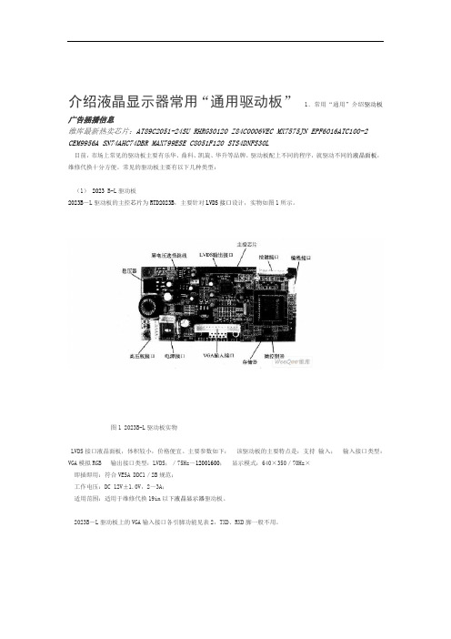
介绍液晶显示器常用“通用驱动板” 1.常用“通用”介绍驱动板广告插播信息维库最新热卖芯片:AT89C2051-24SU RHRG30120Z84C0006VEC MX7575JN EPF6016ATC100-2 CEM9956A SN74AHC74DBR MAX799ESE C8051F120STS4DNFS30L目前,市场上常见的驱动板主要有乐华、鼎科、凯旋、华升等品牌。
驱动板配上不同的程序,就驱动不同的液晶面板,维修代换十分方便。
常见的驱动板主要有以下几种类型:(1)2023 B-L驱动板2023B-L驱动板的主控芯片为RTD2023B,主要针对LVDS接口设计,实物如图1所示。
图1 2023B-L驱动板实物LVDS接口液晶面板,体积较小,价格便宜。
主要参数如下:该驱动板的主要特点是:支持输入;输入接口类型:VGA模拟RGB 输出接口类型:LVDS;/75Hz~12001600;显示模式:640×350/70Hz×即插即用:符合VESA DDC1/2B规范;工作电压:DC 12V±1.0V,2~3A;适用范围:适用于维修代换19in以下液晶显示器驱动板。
2023B-L驱动板上的VGA输入接口各引脚功能见表2,TXD、RXD脚一般不用。
表2 VGA插座引脚功能2023B-L驱动板上的按键接口可以接五个按键、两个LED指示灯,各引脚功能见表3。
表3 2023B-L驱动板上的按键接口引脚功能。
4脚)引脚功能见表30输出接口(LVDS驱动板上的2023B-L输出接口各引脚功能表 4 2023B-L驱动板LVDS。
2023B-L接口引脚功能见表5驱动板上的高压板表5 2023B-L驱动板上的高压板接口引脚功能(2)203B-L驱动板2023B-L主要针对TTL接口设计,其上的LVDS接口为插孔,需要重新接上插针后才能插LVDS插头。
所示。
6驱动板实物如图2023B-T.图6 2023B-T驱动板实物图驱动板体积比2023B-L稍大,价格也相对高一些,其主要参数如下: 2023B-T RGB输入;VGA 输入接口类型:模拟 TTL;输出接口类型::1280~×1024/75 Hz 显示模式:640×350/70Hz 规范;/2B 即插即用:符合VESA DDC1 3A;工作电压:DC 12V±1.0V,2~显示器的驱动板。
超特克HV9918DB1高流LED驱动示例板说明书

Supertex inc.HV9918DB1High Current LED Driver DemoboardThe HV9918DB1 demoboard is a high current LED driver designedto drive one or two LEDs at 700mA from a 9.0 - 16VDC input. Thedemoboard uses Supertex’s HV9918 hysteretic buck LED driver IC.The HV9918DB1 includes digital control of PWM dimming, which allows the user to dim the LEDs using an external, TTL-compatible square wave source applied between DIM and GND . In this case, the PWM dimming frequency and duty ratio are set by the external square wave source.The demoboard is protected against short circuit and open LEDconditions. It also includes thermal derating of the LED current us-ing an external NTC resistor to prevent over-heating.The bottom of the HV9918DB1 is an exposed copper plane (con-nected to the input ground) which can be connected to a 1” square heatsink (eg: 374324B00035G from Aavid Thermalloy) to allow for operation in higher ambient temperatures without tripping the HV9918’s built-in over temperature protection.General DescriptionInput Connection: Connect the input DC voltage between VIN andGND terminals.Output Connection:Connect the LED(s) between LED+ (anode of LED string) and LED- (cathode of LED string) ter-minals.PWM Dimming Connection:1. If no PWM dimming is required, short PWMD and VDD terminals.2. If dimming using an external PWM dimming source, connect the PWM source between the PWMD and GNDterminals.NTC Thermistor Connection:1. If no thermal derating is required, the NTC terminalcan be left open.2. If thermal derating of the LED current is required, the NTC thermistor can be connected between NTCand GND terminals as shown.ConnectionsSilk ScreenOperation of the BoardThe HV9918DB1 uses Supertex’s HV9918 hysteretic buck LED driver IC to control the LED current. Since the regula-tion method controls both the peak and the valley current in the inductor, the demoboard has excellent line and load regulation.The LED current can be controlled in by PWM dimming. PWM dimming can be achieved in one of two ways:1. Analog control of PWM dimming where a 0-2V sourcecan be applied between NTC and GND terminals (the NTC terminal can also be used for thermal derating of the LED current as explained in the next section).2. Direct control of PWM dimming by applying a TTL com-patible square wave source between PWMD and GND terminals.Analog Control of PWM Dimming / Thermal De-ratingAnalog Control of PWM dimming can be accomplished by applying a 0 – 2.0V DC voltage between NTC and GND (the DC voltage must have a 500μA source/sink capability). In this case, PWMD is connected to VDD and the LEDs are dimmed at 1.0kHz (as set by the capacitor at the RAMP pin of the IC). The duty cycle of the LED current can be adjusted by varying the external voltage at NTC (0V = 0% LED cur-rent and 2.0V = 100% LED current).The same NTC terminal can instead be used to de-rate the LED current based on the LED temperature, if desired. This would reduce the LED current as the LED temperature rises and prevents over-heating of the LED. An NTC resistor can be used to sense the temperature of the LED and this resis-tor can be connected between the NTC and GND terminals of the HV9918DB1. The demoboard is designed to operate with a 100k NTC thermistor which has a B-constant of 4250 (eg: NCP18WF104 from Murata). With this NTC thermistor, the LED current will start dropping at 85ºC and will reach about 350mA at 125ºC.Thermal derating in the HV9918DB1 uses the analog control of PWM dimming function to limit the LED current when the LED temperature rises. During normal operating mode (con-stant LED current; no PWM dimming), the LED current will be PWM dimmed at 1.0kHz. During PWM dimming mode, the thermal derating function limits the maximum PWM dim-ming duty cycle so that the LED current does not exceed the maximum allowable current determined by the thermal derating circuit.Direct Control of PWM DimmingIn the direct control method, the PWM dimming of the LEDs is achieved by driving the PWMD terminal using an external square wave source. In this case, PWM dimming frequency and duty cycle are set by the external source.In this mode, if the thermal derating function is not desired, NTC terminal should be left open. In this case, the recom-mended PWM dimming frequency can be anything up to 10kHz.If thermal derating is desired, then the NTC thermistor should be connected between the NTC and GND terminals. In this case, the PWM dimming frequency should be greater than 1.2kHz.Fig. 1. Normal Operation – Drain Voltage and LED CurrentFig. 2. PWM Dimming WaveformFig. 3. PWM Dimming – Rising Edge WaveformFig. 4. PWM Dimming – Falling Edge WaveformFig. 5. Transient Response of LED Current to a Step Changein Input Voltage from 12V to 32VFig. 6. PWM Dimming of LED current with 2.78k between NTC and GNDFig. 7. Efficiency vs. Input Voltage798183858789Input Voltage (V)E f f i c i e n c y (%)Fig. 8 Line Regulation of LED Current0.711Input Voltage (V)L E D C u r r e n t (A )Fig. 9 Switching Frequency vs. Input Voltage100150200250300350400450500550Input Voltage (V)S w i t c h i n g F r e q u e n c y (k H z )LED Current vs NTC TemperatureTemperature (C)L E D C u r r e n t (%)Fig. 10. Thermal Derating of the LED CurrentII Normal inductor current waveformII 0Note:The increase in the LED current at 9.0V input and 6.7V output can be explained by the fact that when the dif-ference between the input and output voltages is very small, the rising inductor current waveform becomes more exponential rather than linear (the falling edge of the inductor current remains linear because the output voltage is high). This causes the average inductor (and therefore LED) current to increase even though the up-per and lower bounds are still the sameHV9918DB1 Schematic DiagramHV9918DB1 WaveformsSupertex inc. does not recommend the use of its products in life support applications, and will not knowingly sell them for use in such applications unless it receives an adequate “product liability indemnification insurance agreement.” Supertex inc. does not assume responsibility for use of devices described, and limits its liability to the replacement of the devices determined defective due to workmanship. No responsibility is assumed for possible omissions and inaccuracies. Circuitry and specifications are subject to change without notice. For the latest product specifications refer to the Supertex inc. (website: http//)©2013 Supertex inc.All rights reserved. Unauthorized use or reproduction is prohibited.Supertex inc.。
奇晶飞升PCB800182产品中文规格书
LVDS 信号
11
LAX2-
LVDS 信号
12
LAX2+
LVDS 信号
13
GND
14
LACK-
15
LACK+
LVDS 信号
16
GND
LVDS 信号
17
LAX3-
LVDS 信号
18
LAX3+
LVDS 信号
19
GND
GND
20
NG
液晶屏接口 1
请参见 EJ070NA-01J 屏规 格书
6 运输,存储,使用要求 1,不要重压和弯折变形 2,防静电和水 3,相对湿度,小于 80% 4, 使用温度 -1-度--+60 度 5,使用湿度 0-+40 度
特殊
支持 LED 背光驱动
4 产品外观尺寸 5 产品结构说明 驱动板尺寸:54.2MMX27.5MM
6:驱动板实物图:
7,AD 板接口功能说明 序号
1 2 3 8 接口功能详细说明 8.1
接口 6PIN CON3 CON1
说明 LED 背光控制输入 LVDS 信号输入 液晶屏接口
6PIN 接口(此接口,默认不按装需要调整,请参见以下技术调整说明)
如有其它相关的此驱动板相关的技术类问题,请致电我公司,
2 特性说明 输入信号 接口
电源
LBIT(默认)
标准 LVDS 信号接 DF14-20P 口
屏接口 INVERTER 接口
40PIN-0.5MM 标准 EJ080NA-04C 定义 6PIN 标准插座(默认不安装)
输入电源
同屏供电 3.3V(不需要另外设置)
背光供电类型
R33
ED10-C_驱动板_0015G1 19.0042
12 1 1 1 2 11 5 7 3 4 1 1 4 2 1
C7,C16,C31,C33,C34,C55,C62,C110,C304 片状陶瓷电容器-50V-0.1μF±10%-X7R-0805-1.35mm ,C305,C306,C361 C23 C32 C13 C12,C24 片状陶瓷电容器-50V-22pF±5%-NPO-0603-0.9mm 片状陶瓷电容器-50V-0.01μF±10%-X7R-0603-0.9mm 片状陶瓷电容器-50V-4700PF±10%-X7R-06030.9mm 片状陶瓷电容器-25V-4.7uF±10%-X7R-1206-1.8mm
16 17 18 19 20 21 22 23 24
18.2.02.0027 18.2.02.0035 18.2.02.0036 18.2.02.0045 18.2.02.0050 18.2.02.0137 18.2.02.0065 18.2.02.0072 18.2.02.0112
2 OF 7
25 26 27 28 29 30 31 32 33 34 35 36 37 38 39
法拉 C212J103K40F400 法拉 C203A104K01CD3A 华星 CT81-Y5P电容-471K-1KV 华星 Y2电容-Y5V-472M-250VAC 华星 Y2电容-Y5V-222M-250VAC ED10GT1 TYCO 0Z-SS-112LM1 TAIYO BK2125HS101-T ON BAS16LT1G ON MUR460RLG ON MURS160T3G ON BZX84C18LT1G ON BZX84C16LT1G VISHAY VS-12CWQ10FNPBF VISHAY BYV26E-TAP
深圳步科电气有限公司
液晶显示器常用“驱动板”介绍

液晶显示器常用“驱动板”介绍液晶显示器作为现代显示技术的代表,其应用领域越来越广泛。
在基于液晶显示器的各种设备中,驱动板是重要的组成部分,在液晶显示器中起到了关键的作用。
通过驱动板的工作,液晶显示器可以得到相应的电源信号,驱动像素点的亮度和颜色,实现显示。
液晶显示器常用的驱动板有很多,其中比较常用的有T-CON驱动板、模组驱动板、LED驱动板等,下面将分别介绍。
T-CON驱动板:T-CON驱动板也称为LVDS驱动板,通常用于笔记本电脑和一些小型液晶屏幕。
T-CON驱动板的主要作用是把来自主板上显示芯片的数字信号转换成模拟信号,然后通过LVDS电缆把信号传输到液晶显像素点上,从而实现显示。
T-CON驱动板具有简单、稳定、易于维修等特点,是小型液晶显示器中普遍采用的一种驱动方式。
模组驱动板:模组驱动板是液晶电视、液晶显示器中常用的一种驱动方式。
它主要由数字信号处理器、驱动芯片和电源组成。
模组驱动板通常被集成在LCD模组中,因此也称为LCD 驱动模块。
模组驱动板的主要作用是将来自主板上的数字信号逐层转换成模拟信号,再通过RGB接口输出到液晶显示屏幕中,实现显示。
模组驱动板具有分层显示、高清晰度、颜色鲜艳等特点,是大型液晶显示屏幕的主流显示方式。
LED驱动板:LED驱动板是由电源、控制芯片、放大器、OCP保护等元件组成的一种电路板。
它主要被用于LED背光液晶显示屏中,通过控制整个屏幕的亮度来实现显示。
LED驱动板的工作原理是先将来自主板上的数字信号转换成模拟信号,再将其输出到LED背光驱动芯片,由驱动芯片控制LED灯的亮度,从而实现整个屏幕的亮度调节。
LED驱动板具有功率稳定、能效高、成本低等优点,是现代液晶显示设备中广泛应用的驱动方式之一。
经过上述的介绍可以看出,液晶显示器中不同的驱动板具有不同的特点和应用范围。
根据不同的需求,我们可以选择不同类型的驱动板,以实现不同的显示效果。
液晶显示器不仅在个人娱乐和办公领域有广泛应用,也在医疗、汽车、教育、军事等领域发挥着重要的作用。
东裕光电科技有限公司产品规格书:对射式(槽型)光电开关DY-ITR9809说明书
广州市东裕光电科技有限公司GUANGZHOU TONYU TECHNOLOGY CO.,LTD产品规格书SPECIFICATION客户名称CUSTOMER 产品名称PRODUCTION对射式(槽型)光电开关Transmissive Sensor 产品型号MODEL DY-ITR9809版本号VERSION NOA1.0地址(Add):广东省广州市番禺区石基镇海涌路3号10号厂房2楼电话(Tel):************传真(Fax):************邮箱(E-mail):************网址(Net):客户确认CUSTOMER CONFIRMATION 审核CHECKED BY编制PREPARED BY汪建新陈少龙DY-ITR9809产品描述Descriptions●侧面安装对射式(槽型)光电开关。
(A side mounting transmissive sensor)产品特性Features●可靠性高(High reliability)●响应时间快(Fast response time)●解析度高(High analytic)●敏感度高(High sensitivity)●无铅(Pb free)●符合RoHS要求(This product itself will remain within RoHS compliant version)●符合欧盟REACH要求(Compliance with EU REACH)产品应用Applications●鼠标(Mouse Copier)●码盘(Switchc Scanner)●非接触式开关(Non-contact Switching)●智能家电(Smart Appliances)包装方式Packing Quantity Specification●袋装:150PCS/袋,5袋/小盒,10小盒/箱(150PCS/1Bag,5Bags/1Box,10Boxes/1Carton)一、外形图Outline dimensions:注(Notes):1、所有尺寸均以毫米为单位(All dimensions are in millimeters)。
超特克LED驱动演示板HV9930DB1说明书
Supertex inc.HV9930DB1General DescriptionThe HV9930DB1 is an LED driver demoboard capable of driving up to 7 1-watt LEDs in series from an automotive input of 9 - 16VDC. The demoboard uses Supertex’s HV9930 in a boost-buck topology. The converter operates at frequencies in excess of 300kHz and has excellent output current regulation over the input voltage range. It can also withstand transients up to 42V and operate down to 6V input. The converter is also protected against open LED and output short circuit conditions. Protection against reverse polarity up to 20V is also included.Board Layout and Connection DiagramHigh Bright LED Driver IC DemoboardMeeting Automotive RequirementsConnections:Input - The input is connected between the terminals of connector J1 as shown in the Connection Diagram.Output - The output is connected between the terminals of connector J2 as shown.Enable/PWM Dimming:To just enable the board, short pins 1 and 2 of connector J3 as shown. For PWM dimming, connect the external push-pullsquare wave source between terminals 1 and 3 of connectorJ3 as shown by the dotted lines.Note: During PWM dimming, pin 2 of connector J3 should be left open. Also, the PWM signal must have the proper polarity with the positive connected to pin 1 of J3. Note that pin 3 of J3 is internally connected to the return path of the input voltage.Actual Size: 2.25” x 1.25”PWM DimmingV INTesting the Demo BoardNormal Operation: Connect the input source and the output LEDs as shown in the Connection Diagram and enable the board. The LEDs will glow with a steady intensity. Connect-ing an ammeter in series with the LEDs will allow measure-ment of the LED current. The current will be 350mA +/- 5%.Open LED test: Connect a voltmeter across the output ter-minals of the HV9930DB1. Start the demoboard normally, and once the LED current reaches steady state, unplug one end of the LED string from the demoboard. The output volt-age will rise to about 33V and stabilize.Short Circuit Test: When the HV9930DB1 is operating in steady state, connect a jumper across the terminals of the LED string. Notice that the switching frequency drops, but the average output current remains the same.PWM Dimming: With the input voltage to the board discon-nected, apply a TTL compatible, push-pull square wave sig-nal between PWMD and GND terminals of connector J3 as shown in the Connection Diagram. Turn the input voltage back on and adjust the duty cycle and / or frequency of the PWM dimming signal. The output current will track the PWMdimming signal. Note that although the converter operates perfectly well at 1.0kHz PWM dimming frequency, the best PWM dimming ratios can be obtained at lower frequencieslike 100 or 200HzTypical ResultsFig. 1 shows the efficiency plot f or the HV9930DB1 over the input voltage range. The converter has efficiencies greater than 80% over 13V input. Note that these measurements do not include the 0.3 - 0.5W loss in the reverse blocking diode.Fig. 2 shows the variation of the switching frequency over the input votage range. The frequency varies from 300kHz to 500kHz over the entire input voltage range and avoids the restricted frequency band of 150kHz to 300kHz and the AM band greater than 530kHz. This makes it easier to meet the conducted and radiated EMI specifications for the automo -tive industry.Fig.3 shows the output current variation over the input volt-age range. The LED current has a variation of about 2.0mA over the entire voltage range.7072747678808284Input Voltage (V)E f f i c i e n c y (%)300350400450500Input Voltage (V)S w i t c h i n g F r e q u e n c y (k H z )348.0348.5349.0349.5350.0350.5Input Voltage (V)O u t p u t C u r r e n t (m A )Fig. 3 Output Current vs. Input VoltageThe waveforms in Fig.4 show the drain voltage of the FET (channel 1 (blue); 10V/div) and the LED current (channel 4 (green); 100mA/div) at three different operating conditions – 9.0V in, 13.5V in and 16V in.Fig. 5 shows the operation of the converter during cold crank conditions as the input voltage decreases from 13.5V to 6V and increases back to 13.5V. In these cases, the input current reaches the limit set and the output current drops correspondingly. Thus, the LEDs continue to glow, but with reduced intensity. Once the voltage ramps back up, the out-put current goes back to its normal value and the converter comes out of the input current limit.Fig.6 shows the LED current during an input step change from 13.5 to 42V and back to 13.5V (similar to a clamped load dump). It can be seen that the LED current drops brieflywhen the input voltage jumps, but there are no overshoots.(a)(b)(c)Fig. 4. Steady State Waveforms(a): 9.0V in; (b): 13.5V in; (c): 16V inFig. 5. Cold Crank OperationChannel 1 (blue): Input voltage (10V/div)Channel 3 (pink): Input current (1A/div)Channel 4 (green): LED current; 100mA/divFig. 6 LED current during step changesin the input voltageChannel 1(blue): Input voltage (10V/div)Channel 4 (green): LED current (100mA/div)Fig. 7a shows the operation of the converter during an Open LED condition and Fig. 7b shows the operation during output short circuit condition. In both cases, it can be seen that the HV9930DB1 can easily withstand faults and come back into normal operation almost instantly.Fig. 8 shows the PWM dimming performance of the HV9930DB1 with a 100Hz, 3.3V square wave signal. The converter can easily operate at PWM dimming duty cyclesfrom 1% - 99%.(a): Open LED Condition(b): Output Short CircuitFig. 7 HV9930DB1 during output fault conditionsFET drain voltage (20V/div)Channel 1 in (a); Channel 2 in (b)Channel 4 (green): LED currentShort Circuit(a)(b)(c)Fig. 8 PWM Dimming at 100HzChannel 1 (blue): PWM Dimming Input Signal (2V/div)Channel 4 (Green): LED current (100mA/div)Fig. 9 shows the rise and fall times of the output current dur-ing PWM dimming. The converter has nearly symmetric rise and fall times of about 25µs. These rise and fall times can be reduced (if desired) by reducing the output capacitance C10. However, this will lead to increased ripple in the output current.Conducted EMI Tests on theHV9930DB1In preliminary tests conducted on the demo board, the board meets SAE J1113 Class 3 conducted EMI standards without the need for any input filters (other than the input capacitors already included). This is a result of the combination of the continuous input current and a localized switching loop (Q1 – C1 – D3).Table 1 details the conducted EMI limit as per SAE J1113 and the maximum conducted EMI obtained from measure-ments on the board. The table also lists the Class of the SAE standard the board meets in each frequency range.The conducted EMI plots for the HV9930DB1 obtained at an input voltage of 13.5V and an LED string voltage of 27V(output current is 350mA) are given in the Appendix. Fig. 9. PWM Dimming rise and fall timesChannel 1 (blue): PWM Dimming Input Signal (2V/div)Channel 4 (Green): LED current (100mA/div)(a): rise time(b): fall timeHV9930DB1 Circuit Schematic:PCB Top LayerPCB Bottom LayerAppendix – Conducted EMI Test ResultsAppendix – Conducted EMI Test Results (cont.)Ref. Level = 65dBµVRef. Level = 49dBµVSupertex inc. does not recommend the use of its products in life support applications, and will not knowingly sell them for use in such applications unless it receives an adequate “product liability indemnification insurance agreement.” Supertex inc. does not assume responsibility for use of devices described, and limits its liability to the replacement of the devices determined defective due to workmanship. No responsibility is assumed for possible omissions and inaccuracies. Circuitry and specifications are subject to change without notice. For the latest product specifications refer to the Supertex inc. (website: http//)©2013 Supertex inc.All rights reserved. Unauthorized use or reproduction is prohibited.Supertex inc.。
液晶AV驱动板规格书-AdafruitIndustries
液晶驱动板规格书产品名称 PCB-800099驱动板文件编号 TYT20120909供应商:深圳市天宇朗通科技有限公司地址:深圳福田区振华路高科德电子市场42073联系人 张先生客户名称:客户地址:联系人文件级别 公共文件发布日期2012-09-091.产品说明:本驱动板可以1,1路VGA信号输入2,2路A V信号输入3,1路HDMI信号输入,且本IC支持的是HDMI1.14,1路倒车信号输入5,支持宽电压输入,并可以在,5V-24V之间正常工作,6,标准背光6PIN,接口,可外接高压板7,驱动板集成液晶屏LED背光驱动板路,8,标准LVDS信号输出,可支持单6,单8,双6,双8等标准的LVDS信号的液晶屏,但只支持屏供电为3.3V的液晶屏9,标准按键板接口,并支持双色LED指示灯显示10,支持TTL信号输出,可支持AT070TN92,AT065TN14AT080TN52AT090TN12AT090TN10AT070TN90AT070TN93AT070TN94等,通用50PIN接口的TTL液晶屏11,配合本公司编号为PCB800100的液晶屏转接板,可支持如下液晶屏EJ070NA01-1024X600分辨率EJ080NA04B-1024X768分辨率ZJ070NA01,型号的通用40PIN高分液晶屏12,配合PCB800100,还可以支持4。
3,5,6,7寸,40PIN通用的屏,定义参见AT0543TN24V,113,本驱动板最大输出显示分辨率为,1920X1080超过,1440X900显示分辨率时,需要视IC的工作情况,增加散热片,以降低IC的工作温度)14本IC,VGA部分可以直接输入YPBPR信号,通过程序实现15,本驱动板可增加遥控功能(需要通过软件实现)16,本驱动板可以自动检测,并显示相关的输入电压信息-----注,此功能为定制功能,需要联系我公司技术部17,本驱动板可以支持自动检测信号开关机功能,--此功能为定制功能18,本驱动板可以加BNC接口---需要定制19,支持倒车控制,并显示A V2上,倒车电压支持50V以内的电压输入20,本驱动板定位孔为四个,21,如果特殊要求,我公司可以提供其它的定制服务22,客户需要改程序,需要连接我公司,购买相关的程序下载板,23,利用本公司的USB接口程序下载板,可以自行在BIN代码上添加LOGO6产品尺寸图7接口功能详细说明7.1CON1,接口定义8 运输,存储,使用要求1,不要重压和弯折变形 2,防静电和水3,相对湿度,小于80% 4, 使用温度 -1-度--+60度 5,使用湿度0-+40度。
液晶万能驱动板HDVX9-CS V29 TV板的说明书
HDVX9-CS-V29 液晶电视驱动板
Ø CON8 (2 X 20PIN/2.0mm双列排针):LVDS接口
脚序号
1 2 3 4 5 6 7 8 9 10 11 12 13 14 15 16 17 18 19 20 21 22 23 24 25 26 27 28 29 30
定义
VCC VCC VCC GND GND GND TXA0M TXA0P TXA1M TXA1P TXA2M TXA2P GND GND TXACKM TXACKP TXA3M TXA3P TXB0M TXB0P TXB1M TXB1P TXB2M TXB2P GND GND TXBCKM TXBCKP TXB3M TXB3P
描述
屏供电 屏供电 屏供电 地 地 地 LVDS奇数线对0 负极 LVDS奇数线对0 正极 LVDS奇数线对1 负极 LVDS奇数线对1 正极 LVDS奇数线对2 负极 LVDS奇数线对2 正极 地 地 LVDS奇数线时钟 负极 LVDS奇数线时钟 正极 LVDS奇数线对3 负极 LVDS奇数线对3 正极 LVDS偶数线对0 负极 LVDS偶数线对0 正极 LVDS偶数线对1 负极 LVDS偶数线对1 正极 LVDS偶数线对2 负极 LVDS偶数线对2 正极 地 地 LVDS偶数线时钟 负极 LVDS偶数线时钟 正极 LVDS偶数线对3 负极 LVDS偶数线对3 正极
脚序号 1 2 3 4 5 6 7 8 9 10 11 12 13 14
定义 K7 CHCH+ MENU TV/AV VOLVOL+ GND LED-G LED-R STB GND IR-IN +5V-S
未定义 节目减 节目加 菜单 信源 音量减 音量加 地 指示灯_绿 指示灯_红 电源 地 遥控接收输入 接收供电
- 1、下载文档前请自行甄别文档内容的完整性,平台不提供额外的编辑、内容补充、找答案等附加服务。
- 2、"仅部分预览"的文档,不可在线预览部分如存在完整性等问题,可反馈申请退款(可完整预览的文档不适用该条件!)。
- 3、如文档侵犯您的权益,请联系客服反馈,我们会尽快为您处理(人工客服工作时间:9:00-18:30)。
液晶驱动板规格书
产品名称 PCB-800099驱动板文件编号 TYT20120909
供应商:深圳市天宇朗通科技有限公司
地址:深圳福田区振华路高科德电子市场42073
联系人 张先生
客户名称:
客户地址:
联系人
文件级别 公共文件
发布日期2012-09-09
1.产品说明:
本驱动板可以
1,1路VGA信号输入
2,2路A V信号输入
3,1路HDMI信号输入,且本IC支持的是HDMI1.1
4,1路倒车信号输入
5,支持宽电压输入,并可以在,5V-24V之间正常工作,
6,标准背光6PIN,接口,可外接高压板
7,驱动板集成液晶屏LED背光驱动板路,
8,标准LVDS信号输出,可支持单6,单8,双6,双8等标准的LVDS信号的液晶屏,但只支持屏供电为3.3V的液晶屏
9,标准按键板接口,并支持双色LED指示灯显示
10,支持TTL信号输出,
可支持AT070TN92,
AT065TN14
AT080TN52
AT090TN12
AT090TN10
AT070TN90
AT070TN93
AT070TN94等,通用50PIN接口的TTL液晶屏
11,配合本公司编号为PCB800100的液晶屏转接板,可支持如下液晶屏
EJ070NA01-1024X600分辨率
EJ080NA04B-1024X768分辨率
ZJ070NA01,型号的通用40PIN高分液晶屏
12,配合PCB800100,还可以支持4。
3,5,6,7寸,40PIN通用的屏,定义参见AT0543TN24V,1
13,本驱动板最大输出显示分辨率为,1920X1080超过,1440X900显示分辨率时,需要视IC的工作情况,增加散热片,以降低IC的工作温度)
14本IC,VGA部分可以直接输入YPBPR信号,通过程序实现
15,本驱动板可增加遥控功能(需要通过软件实现)
16,本驱动板可以自动检测,并显示相关的输入电压信息-----注,此功能为定制功能,需要联系我公司技术部
17,本驱动板可以支持自动检测信号开关机功能,--此功能为定制功能
18,本驱动板可以加BNC接口---需要定制
19,支持倒车控制,并显示A V2上,倒车电压支持50V以内的电压输入
20,本驱动板定位孔为四个,
21,如果特殊要求,我公司可以提供其它的定制服务
22,客户需要改程序,需要连接我公司,购买相关的程序下载板,
23,利用本公司的USB接口程序下载板,可以自行在BIN代码上添加LOGO
6产品尺寸图
7接口功能详细说明7.1
CON1,接口定义
8 运输,存储,使用要求
1,不要重压和弯折变形 2,防静电和水
3,相对湿度,小于80% 4, 使用温度 -1-度--+60度 5,使用湿度0-+40度。