Pulse Density Modulation for software DACs
手机维修英汉小词典

手机维修英汉小词典一、专业术语GSM------------- Global System for Mobile Communication(全球移动通信系统)CDMA-----------Code Division Multiple Access(码分多址)WCDAM--------Wideband CDMA(宽带CDMA) GPRS-------------General Packet Radio Service(通用分组无线业务)MMS--------------Multimedia Messaging Service(多媒体消息业务)SMS---------------Short Message Service(短消息业务)BGA---------------Ball Grid Array(球栅阵列)QA-----------------Quality Assurance(质量保证) QC-----------------Quality Control(质量管理) PLL----------------Phase Locked Loop(锁相环) LCD---------------Liquid Crystal Display(液晶显示)LED----------------Light-emitting Diode(发光二极管)ERP-----------------Enterprise Resources Planning(企业资源规划)OEM----------------Original Equipment Manufacture(原始设备制造商)SMD----------------Surface Mounted Device(表面安装元件)IMEI----------------International Mobile Equipment Identity(国际移动设备识别)二、手机电路图名称注解VCO---------------Voltage-controlledOscillator(压控振荡器)PA-------------------Power Amplifier(功率放大器) TX-------------------Transmit/Tramsmitter(发射/发射机)RX-------------------Receiver Signal Level(接收的信号强度)TPU------------------Timing Processor Unit(定时处理单元)PCB------------------Print Circuit Board(印刷电路板)三、1、逻辑控制部分名称注解VBATT 电池电压BSI 电池类型检测BTEMP 电池温度检测GND-----------------(Ground) 地、电池负极MCU 微处理器单元CCONT 电源模块UPP 通用电话处理器UEM 通用电源管理模块SLEEPCLK 休眠时钟SLEEP 休眠时钟控制PWR 开/关机键PWRONX 开/关机控制信号VBB 逻辑(基带)供电VCORE CPU核心供电VCOBBA 音频模块供电VREF 参考供电VXO 主时钟供电VANA 音频电路供电VFLASH-1 逻辑界面供电VFLASH-2 收音机电路供电VIO 逻辑供电PURX 电源复位CCONTCSX 开机维持CARDDET 卡检测GENSIO 通用输入/输出口CNTVR-1 稳压器控制信号-1 FLASH 字库SRAM 闪存EEPOM 码片ESYSRESET 系统复位ROMSELX 字库片选RAMSELX 暂存片选EEPROMSELX 码片片选ENABLA 使能信号MCUDA CPU数据总线MCUAD CPU地址总线RFC(=RFCLK) 主时钟信号FBUS(1:0) 全双工串行通讯口FBUSRX 双工串行接收FBUSTX 双工串行发送MBUS 编程时钟VPP 字库编程电源2、音频/充电控制部分名称注解COBBA 音频处理器COBBAIF 音频接口COBBACLK 音频(13M)时钟COBBASDA 音频数据COBBACSX 音频片选PCM 脉冲编码调制PCMDCLK 脉冲编码帧时钟PCMSCLK 脉冲编码数据时钟PCMRXDATA 脉冲编码接收数据PCMTXDATA 脉冲编码发送数据IQDATA(1:0)IQ数据总线COBBAIDA I数据线COBBAQDA Q数据线MICP 麦克风信号正MICN 麦克风信号负XMICXP 外部麦克风信号正XMICN 外部麦克风信号正EAR (内部)耳机XEAR 外部耳机HEADDET 外部耳机检测HEADINT 外部耳机中断HOOKDET 免提检测MICBIAS MIC供电控制信号MICDATA MIC数据线EARDATA EAR数据线AUDIO(6:0) 音频输入输出接口XAUDIO(17:0) 外部音频输入输出接口VIN 充电电源输入LOW-BATT 低电检测ICHAR 充电电流检测CCONTINT 电源模块中断PWM 脉冲宽度调制PWM-OUT (充电)脉宽调制控制CHARLIM 充电终止信号CCUT 低电保护充电控制信号3、接收电路名称注解VSYN-1 频率合成器供电-1 VSYN-2 频率合成器供电-1 VRX 接收供电VCP 鉴相器供电VSRM 5V升压VSYNPWR 频率合成器电源启动VXOPWR 主时钟供电控制RXREF 接收解调器参考电压VREFRF01 射频模块参考电压VREFRF02 接收解调器参考电压ANT 天线VANT-1 天线开关控制信号-1 DUPLEX 双工器LNA 低噪声放大器BAL 平衡变换(拜仑)VHFVCO V频段压控振荡器UHFVCO U频段压控振荡器SHFVCO S频段压控振荡器OUT-CP 锁相控制信号LO-OUT 本振信号输出SCLK 频率合成器时钟SDATA 频率合成器数据SENA 频率合成器启动AFC 自动频率控制信号HAGAR 射频信号处理器HARAG-RESET-X 射频IC复位HLGA 射频信号处理器RXC 接收增益控制RX-I/Q 接收基带信号RXIP 接收基带I信号正RXQP 接收基带Q信号正四、发射电路名称注解TX-I/Q 发射基带信号TXIP 发射基带I信号正TXIN 发射基带I信号负TXQP 发射基带Q信号正TXQN 发射基带Q信号负VR2 稳压器2输出(发射供电)VTX 发射供电VMOD(=VTX) 发射调制器供电TXP(=TXPWR) 发射启动信号TXC 发射增益控制VAPC-G GSM自动功率控制VAPC-D DCS自动功率控制TXBUFF 发射缓冲(预放)供电TXVGSM GSM发射控制信号TXVDCS DCS发射控制信号DET0 功率检测信号五、界面电路名称注解LCDCLK 显示时钟LCDSDA 显示串行数据LCDCD 显示控制/数据说明信号LCDEN 显示启动LCDRSTX 显示复位KBLIGHT 键盘灯控制信号VIBRA 振动控制信号BUZZER 振铃控制信号ROW(5:0) 键盘行线COL(4:0) 键盘列线LCD-LIGHT 显示背光灯LCDLED-ADJ 显示背光灯调节KBD-LIGHT 键盘背光灯KBDLED-ADJ 键盘背光灯调节IRONX 红外线接口启动信号常用术语表序号英文标识中文解释英文解释1ACI附件控制接口Accessory Control Interface 2ADC模拟数字转换器Analog Digital Connector3AEC回声消除器4AFC自动频率控制5AGC自动增益控制6AIF应用接口7AES 自动电子快门8ALG 光线指南9ALS 光线感应器10ALWE背景噪声抑制器11AMS售后服务12API应用遍程接口13ARM 高级处理器结构Advanced RISC Machines14ASIC专用集成电路Application Specific Integrated Circuit 15ATR 复位应答Answer To Reset16AUX 辅助设备17AWB 自动白色平衡18BB 基带Baseband19BSI 电池类型识别Battery size Indicator20CACHE 高速缓冲存储器21CBUS 将UPP_WD2与AEM和UEM连接的控制总线control bus(internal phone interfacebetween UPP-UEM22CCI照相机控制接口23CCP内置的照相机口24CDS 相关的双重取样25CIF 通用中间格式26CIS PCMCIA卡信息结构27CMT蜂窝式移动电话(MCU和DSP)28CTSI休眠的时钟定时中断Clock Time Sleep and Interrupt 29COG玻璃上的芯片clip on glass30CSP芯片定标组件clip scale package31CSTN颜色超级的扭曲向列相畸变color super twisted nematic 32DAI数字音频接口33DBUS DSP控制总线DSP controlled bus(internal phone interface between UPP-UEM)34DCN偏移消除的控制信号35DLL 动态链接库36DIF 显示屏接口37DMA 直接存储器存取38DRC 动态范围控制器39DSP 数字信号处理器Digital Signal Processor40EAD 外部附件检测External Accessory Detection 41EMC 电磁兼容性Electro Magnetic Compatibility42EQ 均衡器43EFR 增强型全速率44EMI 电磁干扰45ESD 静电释放Electro Static Discharge46FBUS 异步全双工串行总线Fast Bus,asynchronous message bus connected to DSP(communications bus)47FCI Functional cover interface48FPC 柔韧的印刷电路Flexible printed circuit49FR 全速率Full Rate50GENIO 常规使能输入输出51GPIO 通用输入输出General Purpose Input/Output 52HF 集成有"免提"53HSCSD 高速电路交换数据54IF 接口InterFace55IHF 集成免提Integrated Hands Face56IRDA 红外数据57IRED 红外线发射二极管58LED 发光二级管Light Emitting Diode59LNA 低噪音放大器60LPRF 低功率无线频率Low Power Radio Frequency 61LVDS 低压差分信号62MALT Medium And Loud Transducer63MBUS 单线半双工串行总线Asynchronous message bus connected to MCU (phone control interface).Slow message bus for control data64MCU 微控制器装置Micro Control Unit65MDI MCU-DSP接口,经过ASIC寄存器的信息接口66MFI 调制器和滤波器接口67MUX 多路复用器,多路转换器68NTC 负的温度系数,用于温度感应器的温度感应电阻Negative temperatureCoefficient,temperature sensitiveresistor used as a temperature sensor69PA 功放Power Amplifier 70PCI 话机控制接口软件71PCM 脉宽代码调制72PCM SIO PCM音频传输用的异步串总线73PDA 个人数字助理Personal Digital Assistant 74PDM 脉冲密度调制Pulse Density Modulation 75PDRAM 程序/数据RAM Program/Data RAM76PIFA 平面反向的F天线77PLL 锁相环Phase locked loop78PnPHF 即插即用免提Plug and Play Handfree79PUP 通用接口,USARTS和脉冲宽度调制General Purpose IO(PIO),USARTS and Pulse Width Modulators80PWM 脉宽调制81RTC 实时时钟Real Time Clock82SARAM 单通道RAM Single Access RAM83SDRAM 同步动态随机存取存储器84SIM 用户身份识别模块85SG 同步发生器86SMART PCMCIA接口ASIC87SMPS 开关式电源供电Switch Mode Power SUPPLY88SPR 标准产品需求Standard Product Requirements 89STI 串路接口Serial Trace Interface90TG 定时发送器91TXP 功率放大器使能92TXA 功率控制回路使能93TXC 发送器功率电平和斜坡控制94VCM 电压控制模块95VGA 视频图形阵列96VCXO 电压控制的晶体振荡器97VCTCXO 温度补偿的电压控制的晶体振荡器98VCHARDET 充电器检测的门限级Charger detection threshold levelAA 模拟AB 地址总线ACCESSORIES 配件ADC 模拟到数字的转换ADDRESS BUS 地址总线AFC 自动频率控制AFPCB 音频电路板AGC 自动增益控制AGND 模拟地ALARM 告警ALERT 振铃ALRT 铃声电路ALRT-VCC 振铃器电源ANTSW 天线开关AOC-DRIVE 自动功率控制驱动AUDIO 音频AUX 辅助AVCC 音频供电APC 音频处理芯片ANT 天线AUC 鉴权中心A/D 模拟/数字转换AUTO 自动A/L 音频/逻辑板ACCESS 接入APC 自动功率控制BBIT 比特BURST 突发脉冲串BCCH 广播信道BW 带宽BUSY 忙BUS 总线BARRING 限制BCD 二/十进制码BPF 带通滤波器Block Digram 方框图Backlight 背光Base Band 基带(信号)BATT+ 电池BATTERY 电池BIC 总线接口芯片BS 基站BUZZ 振铃BDR 接收数据信号BDX 发送数据信号BKLT-EN 背景灯启/闭控制CCARD 卡CLONE 复制CODE 代码CONNECTOR 连接器CONTACT SERVICER 联系服务商CONTROL 控制COUPLING 耦合CRYSTAL 晶体CS FLASH 闪存片选CS RAM 随机存储器片选CS ROM 只读存储器片选CAR 电压控制/音频/振铃模块CCH 控制信道CDMA 码分多址CONVERTER 变频器CPU 中央处理器CHARGE 充电CLK OUT 逻辑时钟输出CLK SELECT 时钟选择信号CODEC 编码CP-RX RXVCO 接收锁相压控振荡器CP-TX TXVCO 发射锁相压控振荡器DDTMF 双音多频DTX 非连续发送DATA 数据DISABLE 禁用DISTORTION 失真DEINTERLEARING 去交织DECIPHERING 解密DUPLEX 双工Duplex Saparation 双工间隔DCS-LNA275 1800MHz低噪声放大器电压(2.75V)DCS-SEL 频段选择信号之一(1800MHz)DCS-VCO RXVCO频段切换控制信号之一(1800MHz)DEMODULATION 解调DM-CS 发射机控制信号,控制TXVCO和I/O调制器DP-EN 显示电路启动控制D-TX-VCO 1800MHz发射压控振荡器EE-TACS 扩展的全接入通信系统ESN 电子串号E2PROM 可擦写可编程只读存储器EPR 有效辐射功率ENABLE 启用EQUALIZER 均衡器EAR 耳机EL 发光EN 使能ENAB 使能ERASABLE 可擦写EXC 外部EXT 外部的EXT-B+ 外接电源、充电电压输入FFDMA 频分多址FULL DUPLEX 全双工FACCH 快接入控制信道Freq.Offset 频率偏移FILTER 滤波器FCCH 频率校正信道FDOM 反馈GGSM 全球数字移动通信系统Gen.Out 信号发生器输出GMSK 高斯最小移频键控GCAP 电源模块(摩托罗拉)GCAP-CLKeGCLK 电源模块输送到中央处理器的时钟(32.768kHz)GSM-LNA275 900MHz低噪声放大器电压(2.75V)GSM-PINDIODE 功率放大器输出到匹配电路的切换控制信号GSM-SEL 频段切换控制信号之一(900MHz)G-TX-VCO 900MHz发射压控振荡器HHex 十六进制Hamonic Filter 谐波滤波器HAND SET 手持机HARDWARE 硬件HOOK 外接免提电脑HEAD-INT 头戴耳机控制IInsert Card 插入卡Initial 初始化IMSI 国际移动用户识别码IWF 各种业务功能接口I/O 输入/输出ICTRL 供电电流大小控制IFLO 中频本振INFRARED RAY 红外线INT 中断KKEYBOARD 键盘KEY 键、键控KHz 千赫兹KBC 按键列地址线LLPF 低通滤波器LCD 液晶显示器LCD DATA 显示屏数据LCD EN 显示屏使能LCD WR 显示屏写入LINE 连接线、线路LO 本振LOCK 锁定LOGIC 逻辑LOOP FLITER 环路滤波器LSPCTRL 扬声器控制MMIN 移动用户电话识别码MSN 机械序列号MIC 拾音器MS 移动台MODEM 调制解调器MENU 菜单MOD Freq 调制频率MCLK 主时钟MDM 调制解调器MEMORY 存储器MISO 主机输入从机输出(摩托罗拉)Mixed Second 第二混频MOBILE 移动MOD 调制MODIN 调制I信号负MODIP 调制I信号正MODQN 调制Q信号负MODQP 调制Q信号正MOSI 主机输出从机输入MPU 主处理单元(中央处理器)MUC 主控制单元MUTE 静音NNetwork Selection 网络选择NC 未连接、空脚Outgoing Call 呼出OFST 偏置OOutput LVL 输出电平OSC 振荡器ON 开OFF 关OSCILLATE 振荡PPCM 脉冲编码调制PIN 个人识别码PCH 寻呼信道PWR 电源、功率Parameter 参数PC 个人计算机PA 功率放大器PM 调相Phase Err 相位误差PLL 锁相环路Pause 暂停PADRV 功率放大器驱动PCN 个人通信网POWCONTROL 功率控制POWLEV 功放级别PWR 电源PWRSRC 供电选择PWR-SW 开机信号QQuadrature modulation 正交调制Q 正交支路RRF IN/OUT 高频输入/输出Radio Communication Test 综合测试仪、无线通信测试仪RECALL 重呼RANDOM 随机RAM 随机取存储器RESET 复位RADIO 射频、无线电RD 读REED 干簧管REF 参考、基准RFLO 射频本振RFADAT 射频频率合成器数据RFAENB 射频频率合成器启动RSSI 接收信号强度指示RTC 实时时钟控制RX 接收RX IN 接收输入RX ON 接收启动RX OUT 接收输出RRXEN 接收使能RXIFN 接收中频信号负RXIFP 接收中频信号正RXIN 接收I基带信号负RXIP 接收I基带信号正RXQN 接收Q基带信号负RXQP 接收Q基带信号正RETC-BATT 实时时钟电源(后备电池)RF-V1 频率合成器电源(2.75V)RF-V2 射频电源(2.75V)RXVCO-250 VCO电源(2.5V)RX275 接收电路电源(2.75V)RX-ACQ 接收数据传输请求信号RXI 接收I基带信号RXQ 接收Q基带信号SSAW 声表面波滤波器SENSE 传感SIM 客户识别模块SIM CLK 卡时钟SIM DAT 卡数据SIM RST 卡复位SMOC 数字信号处理器SOFTWARE 软件SHORTCUT 短路SPI 外围串行接口SPI CLK 外围串行接口时钟SPI DAT 外围串行接口数据SPK 扬声器SRAM 静态随机存储器START 开始、启动SW 开关SWDC 未稳压电压SYN CLK 频率合成器时钟SYN DAT 频率合成器数据SYN EN 频率合成器使能SYN STR 频率合成器启动SYN TH 频率合成器供电SYNTON 频率合成器开SPKR 受话音频信号SPR- 受话音频信号负(连接听筒负极)SPR+ 受话音频信号正(连接听筒正极)STDBY 待机TTANK 回路TEMP 温度TEMPERATURE 温度THERM 温度监测TP 测试点TRANSFER 传输、转移TX 发送、发射TXEN 发射使能TXOUT 发射输出TXPWR 发射功率TXRF 发射射频TXENT 发射供电TXIN 发射I基带信号负TXIP 发射I基带信号正TXON 发射开TXQN 发射Q基带信号负TXQP 发射Q基带信号正TXVCO 发射压控振荡器TYPE 类型TXVCO-250 发射VCO电源(2.5V)TXI 发射I基带信号TX-KEY-OUT 发射时序控制输出TXQ 发射Q基带信号UUHF 超高频段UNREGISTERED 未注册的UPDATE 升级UP LINK 上行链路VVBATT 电池电压VCO 压控振荡器VCXOCONT 基准振荡器频率控制VHF 甚高频段VIBRATOR 振荡器VPP FLASH 编程控制VRPAD 稳压后电压VSWITCH 开关电压V-BOOST1 升压电源VIB-EN 振荡器启动VREF 参考电源WWATCHDOG 看门狗信号WDG 看门狗WIRELESS 无线WR 写入XXVCC射频供电四、手机的原理一、手机的电路基本结构手机的结构可分为三部分,即射频处理部分、逻辑/音频部分以及输入输出接口部分。
100618-脉冲密度调制
1 引言在数字信号处理中,常常需要将多位数字信号转化为一位数字信号。
例如,在通信领域,接收器接收到经过编码数字语音信号,需将他转化为模拟信号,即将原来模拟语音信号复原。
经过编码语音信号,通常是多位比特流。
因此,如何将多位比特流转化为模拟语音信号,便成为保证通信质量关键。
又如,在一些控制电路中,控制信号是经过计算生成多位数字信号,而这些数字信号必须转化为模拟信号才能对电路进行控制。
因此,如何将多位数字信号转化为符合实际要求模拟信号,则成为控制电路设计者最关心问题。
在传统电路设计中,面对上述问题时,通常选择使用由多个分离电子元器件组成D/A转换器,有时我们也称他为静态D/A转换器。
但是由于静态D/A 转换器组成结构,决定了他在系统中,必须占用一定空间及消耗一定量功率。
于是在那些要求携带方便系统方案中,静态D/A转换器就不得不被替换掉[1]。
于是人们选择所谓“数字基础”D/A转换器。
而用于数字D/A转换方法有2种:PWM(P ulse Width Modulation)脉冲宽度调制和PDM(Pulse Density Modulation)脉冲密度调制。
这种数字D/A转换器所占用物理空间比较小,消耗功率也比较小。
因此,适用于对系统硬件大小以及功耗要求比较严格系统[1]。
早在20世纪40年代,PWM就开始被应用在电话中。
由于PWM局限性,人们在二十年后,提出了PDM调制方法。
但由于当时应用市场尚不成规模,因而这种调制方法一直未能得到广泛关注和应用。
近年来,由于数字技术在各个领域里得到了广泛应用,数字产品飞速发展,数字信号处理开始得到越来越多关注。
于是PDM调制技术重新得到重视,并被应用在不同领域中。
2 PDM基本介绍PDM是一种在数字领域提供模拟信号调制方法。
在PDM信号中,逻辑“1”表示单个脉冲,逻辑“0”表示没有脉冲。
通常逻辑“1”和逻辑“0”是不连续,逻辑“1”比较均匀地分布在每个调制信号周期里。
【2017年整理】DAC解码芯片的泰斗
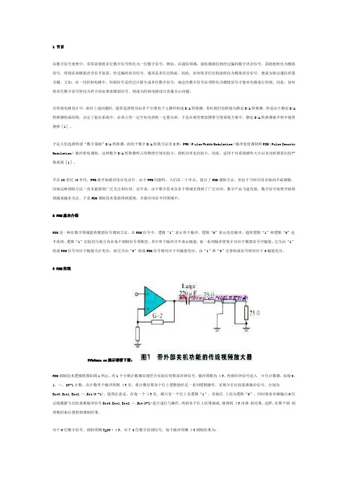
DAC解码芯片的泰斗---转目前,烧友们对DIY/DAC解码器风头正劲,近日从一朋友那里弄来一些关于DAC解码芯片的资料,愿与大家分享。
DAC芯片通常由Crystal、Burr Brown、AKM、Analog这4家公司包揽。
Burr Brown公司隶属于半导体业界著名的重量级厂家德州仪器公司,其最为人熟知的DAC 芯片莫过于PCM1704。
众多Hi End厂家都对其大加赞赏,其中包括不少坚持传统两声道的Hi End厂家,如Mark Levinson最顶级的解码器NO.360(4495美元)就采用了PCM1704。
它是一块精密的24bit D/A转换芯片,拥有超低失真和低电平响应线性。
其采用了2μm BICMOS制造工艺和一种非常独特的示意数量型架构(Sign Magnitude)。
在其内部设计了两个23bit完全互补的D/A转换器,从而取得24bit的精度。
这两个D/A转换器公用一个时钟参考,公用一个R 2R型梯形电阻网络,通过不断分压来取得准确的数位电流源信号。
R 2R梯形电阻网络使用的双平衡电流回路可以确保在任何电平下对电压信号都有理想的跟踪能力。
这两个D/A转换器在内部数据计算上完全独立,可以有非常线性的电平响应,尤其是在低电平(即小音量)下线性良好。
R 2R梯形电阻网络里的电阻都是将镍铬薄膜电阻经激光微调制得的,因此精度足够高。
另外,两个D/A转换器也是经过精密配对才加以使用的。
PCM1704 的信噪比达到了令人惊异的 120dB,并且是标准型 K 级芯片。
其总谐波失真和噪声达到了0.0008%(-101.94 dB),也是标准型K级芯片。
标准型K级的动态范围达到了112dB。
PCM1704的取样频率范围为16~96kHz,过取样频率为96kHz的8倍过取样。
另外,其输入音频数据格式为20bit或24bit,快速电流输出为±1.2mA/200ns,电源电压为±5V。
PDM 麦克风采集中DFSDM的作用

前言STM32 提供了丰富的音频应用外设,并得益于灵活高效的内部架构,可以支持广泛的音频应用。
本文中,在简单介绍音频采集的背景知识后,从应用需求出发,确定麦克风的选用。
然后,描述了STM32 内部DFSDM (Digital Filter for SigmaDelta Modulator)在PDM 麦克风采集中应用。
最后逐步介绍如何利用STM32CubeMX 进行DFSDM 设计开发,实现PDM麦克风声音采集。
一背景知识声音通过声学传感器获取模拟信号,经过模数转换器,转换成二进制码0 和1,这些0 和1 便构成了音频数字信号。
PDM 麦克风能够实现上述的模拟信号获取,并输出PDM 信号。
PDM (Pulse Density Modulation)脉冲密度调制,利用脉冲密度表示模拟信号强度。
从PDM 位流中获取数据,还需要经过如下图环节才能获得模拟信号幅度对应的数字量。
二应用需求及DFSDM 支持分析在音频应用开发前,需要根据应用需求,对麦克风个数、支持编码类型、采样率及分辨率等进行确定。
下面围绕DFSDM在这些需求方面的支持情况进行分析。
2.1 麦克风数量同时运行的最大麦克风数量,对于DFSDM,由DFSDM 中滤波器数量决定。
简单理解,就是一个滤波器对应一个麦克风。
注意这种简单等同并不适用于非同时采样的应用场景。
麦克风的数量不直接对应通道数量,如下图。
可映射任一DFSDM 通道单元至滤波器单元。
对于通道CH(y-1),数据线可来源于DATIN(y-1)引脚,也可来自于DATIN(y),在通道单元中可以选择获取数据的时刻(上升沿或者下降沿)。
这样带来的益处是,可利用内部两个通道单元对同一个数据线上数据进行分离并处理获得采样数据。
而这个应用,直接满足了双通道数据在同一条数据线上的数据采集场景。
上述描述的应用场景中,数据处理流向如下图所示:注1:图中CLK 线硬件设计上不一定需要连接,DFSDM 可在内部关联,实现利用输出时钟作为时钟输入,具体可通过参考手册了解。
mems pdm 电路设计 -回复

mems pdm 电路设计 -回复什么是MEMS(微电子机械系统)?MEMS(微电子机械系统)是一种能够集成在半导体芯片中的微型机械和电子器件。
它利用了微弯曲、微拉伸、微振动等微尺度运动来实现感应、测量、控制和执行动作等功能。
MEMS 的应用领域非常广泛,包括加速度计、压力传感器、陀螺仪、喷墨打印头等。
MEMS PDM(压电电容麦克风)电路设计MEMS PDM是一种采用MEMS技术制造的麦克风,通过压电效应将声波转换为电信号。
PDM 是“Pulse Density Modulation”的缩写,意为脉冲密度调制。
与传统的模拟输出麦克风不同,PDM麦克风通过高速脉冲信号的密度来表示声波,从而降低了电路中的噪声和失真。
PDM电路设计的主要步骤如下:1. 系统需求分析:首先要明确所需的麦克风性能参数,如灵敏度、频率响应等。
根据需求,选择合适的MEMS PDM麦克风。
2. 接口电路设计:PDM麦克风的输出信号是一串由高速脉冲组成的数字信号,需要进行滤波和信号处理来得到与声波相对应的电压信号。
在接口电路中,通常包括可变增益放大器、低通滤波器和模数转换器(ADC)等。
3. 可变增益放大器设计:由于MEMS PDM 麦克风接收到的声音信号幅度较小,需要进行放大。
可变增益放大器可以根据需求调节放大倍数。
设计时要考虑到放大器的噪声性能、带宽、稳定性等因素。
4. 滤波器设计:PDM麦克风输出的数字信号包含高频噪声,需要进行滤波来消除噪声并恢复声音信号。
常见的滤波器设计包括巴特沃斯滤波器、Chebyshev滤波器等。
5. ADC设计:滤波后的信号需要转换为数字信号,常用的方式是采用模数转换器(ADC)。
ADC的选择要考虑采样率、分辨率、功耗等参数,同时也要与后续处理器或系统兼容。
6. 反馈及优化:在整个设计过程中,需要进行反馈和优化。
通过测试和仿真等手段,对电路的性能进行评估并适当调整参数,以满足设计要求。
开关电源需掌握的基本英语词汇

开关电源需掌握的基本英语词汇AAuxiliary supply(辅助电源)BB-H curve(磁化曲线)Bipolar transistor(双极型晶体管)Avalanche(雪崩)base drive(基极驱动)forward bias safe operating area (FBSOA,正向偏置安全⼯作区) reverse bias safe operating area(RBSOA,反向偏置安全⼯作区) safe operating area(安全⼯作区)secondary breakdown( ⼆次击穿)storage time(储存时间)vecovecsBoost converter(Boost 变换器)Compensation(补偿)Control equation(控制等式)Buck converter (Buck 变换器)Compensation(补偿)Control equation(控制等式)Buck-Boost converter(Buck-Boost 变换器)CCapacitor(电容)Aluminum(铝)Ceramic(陶瓷的)EMI filter(EMI 滤波器)Equivalent circuit(等效电路)Equivalent series inductance(等效串联电感)Failure mode(失效模式)Film(薄膜)Flammability(可燃性)Metallized paper(镀⾦属纸)Metallized film(镀⾦属膜)Multilayer ceramic(多层陶瓷的)Niobium(铌)Polymer electrolytic(聚合物电解)Polymer tantalum(聚合物钽)Reservoir(储能的)Ripple current(纹波电流)Self-heating(⾃加热)Tantalum(钽)Temperature coefficient(温度系数)Capacitor definition(电容定义)Charge pump(电荷泵)Clamp circuit(钳位电路)Common mode interference(共模⼲扰)Compensation(补偿)Laboratory method(实验室⽅法)Continuous operation(连续⼯作)Current limit(限流)Current mode PWM controller(电流模式PWM控制器)Current sense(电流检测)Current transformer(电流互感器)DDC-DC converter(直流-直流变换器)Dead time(死区时间)Differential mode interference(差模⼲扰)Diode(⼆极管)Forward recovery(正向恢复)Gallium arsenide(砷化镓,⽓体)Junction(PN结)PIN(引脚)Reverse recovery(反向恢复)Schottky(肖特基)Silicon carbide(sic,碳化硅)Soft recovery(软恢复)Standard recovery(标准恢复)Ultra-fast(超快速)Discontinuous operation(断续⼯作)Dissipation factor(损耗因数)EEddy current(涡流)Electromagnetic compatibility(EMC,电磁兼容)Electromagnetic interference(EMI,电磁⼲扰)Equivalent series resistance(ESR,等效串联电阻)Error amplifier(误差放⼤器)European community(欧盟)FFederal Communication Commission(FCC,美国联邦通信委员会)Ferrite(铁氧体)Flux density(磁通密度)Flyback(反激)Compensation(补偿)Converter(变换器)Flying capacitor(飞跨电容)Forward compensation(前馈补偿)Converter(变换器)Full bridge converter(全桥变换器)Full wave bridge(全桥)GGround fault circuit interrupter(GFCI,接地故障端路器)HHalf bridge converter(半桥变换器)Hold up time(保持时间)Hysteresis (magnetic,磁滞)IIn-rush current(内部冲击电流)Inductor(电感)Shielded(屏蔽的)Temperature(温升)Unshielded(未屏蔽的)inductor definition(电感定义)inverting boost converter(反向Boost变换器)LLenz’s law(楞次定律)MMagnetic force(磁⼒)Metal oxide varistor(MOV,⾦属氧化物可变电阻)Avalanche(雪崩)Avalanche rating (雪崩额定值)Dv/dt rating(dv/dt额定值)Gate capacitance(门极电容)Gate drive(门极驱动)Gate –voltage(门极电压)High side drive(⾼压侧驱动)Intrinsic diode(体⼆级管)Logic drive(逻辑驱动)Low voltage drive(低压驱动0Miller effect(⽶勒效应)On-resistance(导通电阻)P channel devices(P沟道器件)Reverse recovery(反向恢复)RFI suppression(射频⼲扰抑制)Safe operating area(安全⼯作区)Sense fets(电流检测FET)Standard drive(标准驱动)Synchronous rectification(同步整流)Transform drive(变压器驱动)Multiple phase PWM controller(多相PWM控制器)NNTC thermistor(负温度系数热敏电阻)OOff-line supply(离线式电源)Optocoupler(光耦合器)PPassivation(钝化作⽤)Patient-area medical equipment(医疗器械)Permeability(磁导率)Powdered iron(铁粉)Power factor correction(功率因数校正)Power line transients(电⽹瞬变)Pulse frequency modulation controller(脉冲频率调制控制器件)Pulse width modulation controller(脉宽频率调制控制器件)Push-pull converter(推挽变换器)RRadio frequency interference(RFI,射频⼲扰)Resistor(电阻)Carbon composition(碳化合物)Film(薄膜)Wire(导线)Resonant mode controller(谐振模式控制器)SSEPIC converter(SEPIC变换器)Skin effect(集肤效应)Slope compensation(斜坡补偿)Snubber circuit(缓冲电路)Soft start(软启动)Synchronous rectification(同步整流)TTransformer(变压器)AC flux density(交流磁通密度)Clamp winding(钳位绕组)Copper strip(铜带)Core permeability(磁导率)Equivalent circuit(等效电路)Ideal transformer(理想变换器)Magnetizing inductance(激磁电感)Parasitic(leakage) inductance(寄⽣电感,漏感)Pulse transformer(脉冲变压器)Reset(复位)Safety design(安全性设计)Transformer equation(变压器等式)Wire(导线)Transformer isolated converters(变压器隔离的变换器)UUnder voltage lockout(⽋压锁定)Universal input(通⽤输⼊)VVoltage doubler(电压倍增器)Voltage mode PWM controller(电压模式PWM 控制器)WWire table(导线⼀览表)ZZener diode(齐纳⼆极管)。
EFR32FG22无线Gecko专有协议SoC系列产品说明书
EFR32FG22 无线 Gecko SoC 产品系列数据表EFR32FG22无线 Gecko 专有协议 SoC 系列是无线 Gecko 产品系列的组成部分。
EFR32FG22无线 GeckoSoC 是实现 IoT 设备上节能的专有协议连网的理想之选。
这款单芯片解决方案结合了 38.4 MHz Cortex-M33 和高性能 2.4 GHz 无线电,旨在为 IoT 连接应用提供行业领先的节能无线 SoC 。
无线 Gecko 应用包括:主要特点•32 位 ARM® Cortex®-M33 内核,最高工作频率为 38.4 MHz•最高 512 kB 闪存和 32 kB RAM •低有功电流和睡眠电流的节能型射频内核•集成 PA ,TX 功率高达 6 dBm (2.4 GHz)•通过信任根和安全加载程序 (RTSL) 进行的安全启动•可选 OOK 模式的 RFSENSE•电子货架标签•住宅和建筑自动化及安全•工业自动化•商业和零售照明与传感EM4—ShutoffEM3—StopEM2—Deep SleepEM1—SleepEM0—Active| Building a more connected world.Rev. 1.2Copyright © 2023 by Silicon Laboratories1.功能列表EFR32FG22 突出功能如下所列。
•低功耗无线片上系统•高性能 32 位 38.4 MHz ARM Cortex®-M33,带有 DSP 指令和浮点单元,可实现高效的信号处理•高达 512 kB 的闪存程序存储器•高达 32 kB 的 RAM 数据存储器•2.4 GHz 无线电操作•射频性能•在 250 kbps O-QPSK DSSS 的条件下,灵敏度为-102.3 dBm•在 1 Mbit/s GFSK 的条件下,灵敏度为-98.9 dBm•在 2 Mbit/s GFSK 的条件下,灵敏度为-96.2 dBm•TX 功率高达 6 dBm•无线电接收电流为2.5 mA•在 0 dBm 输出功率的条件下,无线电传输电流为3.4 mA•在 6 dBm 输出功率的条件下,无线电传输电流为7.5 mA•低系统能耗•RX 电流为3.6 mA (1 Mbps GFSK)•RX 电流为3.9 mA (250 kbps O-QPSK DSSS)•在 0 dBm 输出功率的条件下,TX 电流为4.1 mA•在 6 dBm 输出功率的条件下,TX 电流为8.2 mA•在 38.4 MHz 活动模式 (EM0) 下,运行功耗为26 μA/MHz•1.20 μA EM2 深度睡眠电流(保留 8 kB RAM,RTC 从 LFRCO 中运行)•0.17 μA EM4 电流•支持的调制格式•2 (G)FSK,可配置完整波形•OQPSK DSSS•(G)MSK•协议支持•专有•广泛的 MCU 外围设备选择•模拟数字转换器 (ADC)•12 位,1 Msps•16 位,76.9 ksps•高达 26 个带有输出状态保持和异步中断功能的通用 I/O 引脚•8 信道 DMA 控制器•12 信道外围设备反射系统 (PRS)•4 个 16 位定时器/计数器(3 个比较/捕获/PWM 通道)•1 个 32 位定时器/计数器(3 个比较/捕获/PWM 通道)•32 位实时计数器•24 位低能耗定时器,用于波形生成•1 个看门狗定时器•2 个通用同步/异步接收器/传输器 (UART/SPI/SmartCard (ISO 7816)/ IrDA/I2S)•1 个增强型通用异步接收器/传输器 (EUART)•2 个 I2C 接口,带 SMBus 支持•数字麦克风接口 (PDM)•可选 OOK 模式的 RFSENSE•单点校准后具有 +/-1.5 摄氏度精度的芯片温度传感器•宽工作范围•单电源1.71 至 3.8 V•-40°C 至 85°C•安全特性•通过信任根和安全加载程序 (RTSL) 进行的安全启动•硬件加密加速,适用于 AES128/256、SHA-1、SHA-2(高达 256位)、ECC(高达 256 位)、ECDSA 和 ECDH•符合 NIST SP800-90 和 AIS-31 标准的真随机数生成器 (TRNG)•ARM® TrustZone®•使用锁定/解锁功能进行安全调试•封装•QFN40 5 毫米 × 5 毫米 × 0.85 毫米•QFN32 4 毫米 × 4 毫米 × 0.85 毫米EFR32FG22 无线 Gecko SoC 产品系列数据表功能列表2EFR32FG22 Wireless Gecko SoC Family Data SheetOrdering Information 2. Ordering InformationTable 2.1. Ordering Information | Building a more connected world.Rev. 1.2 | 3Table of Contents1. Feature List (2)2. Ordering Information (3)3. System Overview (7)3.1 Introduction (7)3.2 Radio (7)3.2.1 Antenna Interface (7)3.2.2 Fractional-N Frequency Synthesizer (8)3.2.3 Receiver Architecture (8)3.2.4 Transmitter Architecture (8)3.2.5 Packet and State Trace (8)3.2.6 Data Buffering (8)3.2.7 Radio Controller (RAC) (8)3.2.8 RFSENSE Interface (9)3.3 General Purpose Input/Output (GPIO) (9)3.4 Clocking (9)3.4.1 Clock Management Unit (CMU) (9)3.4.2 Internal and External Oscillators (9)3.5 Counters/Timers and PWM (9)3.5.1 Timer/Counter (TIMER) (9)3.5.2 Low Energy Timer (LETIMER) (10)3.5.3 Real Time Clock with Capture (RTCC) (10)3.5.4 Back-Up Real Time Counter (BURTC) (10)3.5.5 Watchdog Timer (WDOG) (10)3.6 Communications and Other Digital Peripherals (10)3.6.1 Universal Synchronous/Asynchronous Receiver/Transmitter (USART) (10)3.6.2 Enhanced Universal Asynchronous Receiver/Transmitter (EUART) (10)3.6.3 Inter-Integrated Circuit Interface (I2C) (10)3.6.4 Peripheral Reflex System (PRS) (11)3.6.5 Pulse Density Modulation (PDM) Interface (11)3.7 Security Features (11)3.7.1 Secure Boot with Root of Trust and Secure Loader (RTSL) (11)3.7.2 Cryptographic Accelerator (11)3.7.3 True Random Number Generator (11)3.7.4 Secure Debug with Lock/Unlock (12)3.8 Analog (12)3.8.1 Analog to Digital Converter (IADC) (12)3.9 Power (13)3.9.1 Energy Management Unit (EMU) (13)3.9.2 Voltage Scaling (13)3.9.3 DC-DC Converter (13)3.9.4 Power Domains (13)3.10 Reset Management Unit (RMU) (14)3.11 Core and Memory (14)3.11.1 Processor Core (14)3.11.2 Memory System Controller (MSC) (14)3.11.3 Linked Direct Memory Access Controller (LDMA) (14)3.12 Memory Map (15)3.13 Configuration Summary (16)4. Electrical Specifications (17)4.1 Electrical Characteristics (17)4.2 Absolute Maximum Ratings (18)4.3 General Operating Conditions (19)4.4 DC-DC Converter (20)4.4.1 DC-DC Operating Limits (22)4.5 Thermal Characteristics (23)4.6 Current Consumption (24)4.6.1 MCU current consumption using DC-DC at 3.0 V input (24)4.6.2 MCU current consumption at 3.0 V (26)4.6.3 MCU current consumption at 1.8 V (28)4.6.4 Radio current consumption at 3.0V using DCDC (30)4.7 Flash Characteristics (31)4.8 Energy Mode Wake-up and Entry Times (32)4.9 RFSENSE Low-energy Wake-on-RF (33)4.10 2.4 GHz RF Transceiver Characteristics (34)4.10.1 RF Transmitter Characteristics (34)4.10.2 RF Receiver Characteristics (38)4.11 Oscillators (42)4.11.1 High Frequency Crystal Oscillator (42)4.11.2 Low Frequency Crystal Oscillator (43)4.11.3 High Frequency RC Oscillator (HFRCO) (44)4.11.4 Fast Start_Up RC Oscillator (FSRCO) (45)4.11.5 Low Frequency RC Oscillator (LFRCO) (45)4.11.6 Ultra Low Frequency RC Oscillator (45)4.12 GPIO Pins (3V GPIO pins) (46)4.13 Analog to Digital Converter (IADC) (48)4.14 Temperature Sensor (51)4.15 Brown Out Detectors (52)4.15.1 DVDD BOD (52)4.15.2 LE DVDD BOD (52)4.15.3 AVDD and IOVDD BODs (53)4.16 PDM Timing Specifications (54)4.16.1 Pulse Density Modulator (PDM), Common DBUS (54)4.17 USART SPI Main Timing (55)4.17.1 USART SPI Main Timing, Voltage Scaling = VSCALE2 (56)4.17.2 USART SPI Main Timing, Voltage Scaling = VSCALE1 (56)4.18 USART SPI Secondary Timing (57)4.18.1 USART SPI Secondary Timing, Voltage Scaling = VSCALE2 (57)4.18.2 USART SPI Secondary Timing, Voltage Scaling = VSCALE1 (58)4.19 I2C Electrical Specifications (59)4.19.1 I2C Standard-mode (Sm) (59)4.19.2 I2C Fast-mode (Fm) (60)4.19.3 I2C Fast-mode Plus (Fm+) (61)4.20 Typical Performance Curves (61)4.20.1 Supply Current (62)4.20.2 RF Characteristics (64)4.20.3 DC-DC Converter (65)4.20.4 IADC (65)5. Typical Connections (66)5.1 Power (66)5.2 RF Matching Networks (67)5.2.1 2.4 GHz Matching Network (67)5.3 Other Connections (68)6. Pin Definitions (69)6.1 QFN40 Device Pinout (69)6.2 QFN32 Device Pinout (71)6.3 Alternate Function Table (73)6.4 Analog Peripheral Connectivity (74)6.5 Digital Peripheral Connectivity (75)7. QFN32 Package Specifications (78)7.1 QFN32 Package Dimensions (78)7.2 QFN32 PCB Land Pattern (80)7.3 QFN32 Package Marking (82)8. QFN40 Package Specifications (83)8.1 QFN40 Package Dimensions (83)8.2 QFN40 PCB Land Pattern (85)8.3 QFN40 Package Marking (86)9. Revision History (87)3. System Overview3.1 IntroductionThe EFR32 product family combines an energy-friendly MCU with a high performance radio transceiver. The devices are well suited for secure connected IoT multi-protocol devices requiring high performance and low energy consumption. This section gives a short intro-duction to the full radio and MCU system. The detailed functional description can be found in the EFR32xG22 Reference Manual.A block diagram of the EFR32FG22 family is shown in Figure 3.1 Detailed EFR32FG22 Block Diagram on page 7. The diagram shows a superset of features available on the family, which vary by OPN. For more information about specific device features, consult Ordering Information .RESETnPDnPCnPBnPAnRF2G4_IODVDDVREGVDD VREGSW AVDD PAVDD RFVDD DECOUPLEIOVDD Figure 3.1. Detailed EFR32FG22 Block Diagram3.2 RadioThe Wireless Gecko family features a radio transceiver supporting proprietary wireless protocols.3.2.1 Antenna InterfaceThe 2.4 GHz antenna interface consists of a single-ended pin (RF2G4_IO). The external components for the antenna interface in typi-cal applications are shown in the RF Matching Networks section.Rev. 1.2 | 73.2.2 Fractional-N Frequency SynthesizerThe EFR32FG22 contains a high performance, low phase noise, fully integrated fractional-N frequency synthesizer. The synthesizer is used in receive mode to generate the LO frequency for the down-conversion mixer. It is also used in transmit mode to directly generate the modulated RF carrier.The fractional-N architecture provides excellent phase noise performance, frequency resolution better than 100 Hz, and low energy consumption. The synthesizer’s fast frequency settling allows for very short receiver and transmitter wake up times to reduce system energy consumption.3.2.3 Receiver ArchitectureThe EFR32FG22 uses a low-IF receiver architecture, consisting of a Low-Noise Amplifier (LNA) followed by an I/Q down-conversion mixer. The I/Q signals are further filtered and amplified before being sampled by the IF analog-to-digital converter (IFADC).The IF frequency is configurable from 150 kHz to 1371 kHz. The IF can further be configured for high-side or low-side injection, provid-ing flexibility with respect to known interferers at the image frequency.The Automatic Gain Control (AGC) module adjusts the receiver gain to optimize performance and avoid saturation for excellent selec-tivity and blocking performance. The 2.4 GHz radio is calibrated at production to improve image rejection performance.Demodulation is performed in the digital domain. The demodulator performs configurable decimation and channel filtering to allow re-ceive bandwidths ranging from 0.1 to 2530 kHz. High carrier frequency and baud rate offsets are tolerated by active estimation and compensation. Advanced features supporting high quality communication under adverse conditions include forward error correction by block and convolutional coding as well as Direct Sequence Spread Spectrum (DSSS).A Received Signal Strength Indicator (RSSI) is available for signal quality metrics, for level-based proximity detection, and for RF chan-nel access by Collision Avoidance (CA) or Listen Before Talk (LBT) algorithms. An RSSI capture value is associated with each received frame and the dynamic RSSI measurement can be monitored throughout reception.3.2.4 Transmitter ArchitectureThe EFR32FG22 uses a direct-conversion transmitter architecture. For constant envelope modulation formats, the modulator controls phase and frequency modulation in the frequency synthesizer. Transmit symbols or chips are optionally shaped by a digital shaping filter. The shaping filter is fully configurable, including the BT product, and can be used to implement Gaussian or Raised Cosine shap-ing.Carrier Sense Multiple Access - Collision Avoidance (CSMA-CA) or Listen Before Talk (LBT) algorithms can be automatically timed by the EFR32FG22. These algorithms are typically defined by regulatory standards to improve inter-operability in a given bandwidth be-tween devices that otherwise lack synchronized RF channel access.3.2.5 Packet and State TraceThe EFR32FG22 Frame Controller has a packet and state trace unit that provides valuable information during the development phase. It features:•Non-intrusive trace of transmit data, receive data and state information•Data observability on a single-pin UART data output, or on a two-pin SPI data output•Configurable data output bitrate / baudrate•Multiplexed transmitted data, received data and state / meta information in a single serial data stream3.2.6 Data BufferingThe EFR32FG22 features an advanced Radio Buffer Controller (BUFC) capable of handling up to 4 buffers of adjustable size from 64 bytes to 4096 bytes. Each buffer can be used for RX, TX or both. The buffer data is located in RAM, enabling zero-copy operations.3.2.7 Radio Controller (RAC)The Radio Controller controls the top level state of the radio subsystem in the EFR32FG22. It performs the following tasks:•Precisely-timed control of enabling and disabling of the receiver and transmitter circuitry•Run-time calibration of receiver, transmitter and frequency synthesizer•Detailed frame transmission timing, including optional LBT or CSMA-CA3.2.8 RFSENSE InterfaceThe RFSENSE block allows the device to remain in EM2, EM3 or EM4 and wake when RF energy above a specified threshold is detec-ted. When operated in selective mode, the RFSENSE block performs OOK preamble and sync word detection, preventing false wake-up events.3.3 General Purpose Input/Output (GPIO)EFR32FG22 has up to 26 General Purpose Input/Output pins. Each GPIO pin can be individually configured as either an output or in-put. More advanced configurations including open-drain, open-source, and glitch-filtering can be configured for each individual GPIO pin. The GPIO pins can be overridden by peripheral connections, like SPI communication. Each peripheral connection can be routed to several GPIO pins on the device. The input value of a GPIO pin can be routed through the Peripheral Reflex System to other peripher-als. The GPIO subsystem supports asynchronous external pin interrupts.All of the pins on ports A and port B are EM2 capable. These pins may be used by Low-Energy peripherals in EM2/3 and may also be used as EM2/3 pin wake-ups. Pins on ports C and D are latched/retained in their current state when entering EM2 until EM2 exit upon which internal peripherals could once again drive those pads.A few GPIOs also have EM4 wake functionality. These pins are listed in the Alternate Function Table.3.4 Clocking3.4.1 Clock Management Unit (CMU)The Clock Management Unit controls oscillators and clocks in the EFR32FG22. Individual enabling and disabling of clocks to all periph-eral modules is performed by the CMU. The CMU also controls enabling and configuration of the oscillators. A high degree of flexibility allows software to optimize energy consumption in any specific application by minimizing power dissipation in unused peripherals and oscillators.3.4.2 Internal and External OscillatorsThe EFR32FG22 supports two crystal oscillators and fully integrates four RC oscillators, listed below.• A high frequency crystal oscillator (HFXO) with integrated load capacitors, tunable in small steps, provides a precise timing refer-ence for the MCU. The HFXO provides excellent RF clocking performance using a 38.4 MHz crystal. The HFXO can also support an external clock source such as a TCXO for applications that require an extremely accurate clock frequency over temperature.• A 32.768 kHz crystal oscillator (LFXO) provides an accurate timing reference for low energy modes.•An integrated high frequency RC oscillator (HFRCO) is available for the MCU system, when crystal accuracy is not required. The HFRCO employs fast start-up at minimal energy consumption combined with a wide frequency range, from 1 MHz to 38.4 MHz.•An integrated fast start-up RC oscillator (FSRCO) that runs at a fixed 20 MHz•An integrated low frequency 32.768 kHz RC oscillator (LFRCO) for low power operation where high accuracy is not required.•An integrated ultra-low frequency 1 kHz RC oscillator (ULFRCO) is available to provide a timing reference at the lowest energy con-sumption in low energy modes.3.5 Counters/Timers and PWM3.5.1 Timer/Counter (TIMER)TIMER peripherals keep track of timing, count events, generate PWM outputs and trigger timed actions in other peripherals through the Peripheral Reflex System (PRS). The core of each TIMER is a 16-bit or 32-bit counter with up to 3 compare/capture channels. Each channel is configurable in one of three modes. In capture mode, the counter state is stored in a buffer at a selected input event. In compare mode, the channel output reflects the comparison of the counter to a programmed threshold value. In PWM mode, the TIMER supports generation of pulse-width modulation (PWM) outputs of arbitrary waveforms defined by the sequence of values written to the compare registers. In addition some timers offer dead-time insertion.See 3.13 Configuration Summary for information on the feature set of each timer.3.5.2 Low Energy Timer (LETIMER)The unique LETIMER is a 24-bit timer that is available in energy mode EM0 Active, EM1 Sleep, EM2 Deep Sleep, and EM3 Stop. This allows it to be used for timing and output generation when most of the device is powered down, allowing simple tasks to be performed while the power consumption of the system is kept at an absolute minimum. The LETIMER can be used to output a variety of wave-forms with minimal software intervention. The LETIMER is connected to the Peripheral Reflex System (PRS), and can be configured to start counting on compare matches from other peripherals such as the Real Time Clock.3.5.3 Real Time Clock with Capture (RTCC)The Real Time Clock with Capture (RTCC) is a 32-bit counter providing timekeeping down to EM3. The RTCC can be clocked by any of the on-board low-frequency oscillators, and it is capable of providing system wake-up at user defined intervals.A secondary RTC is used by the RF protocol stack for event scheduling, leaving the primary RTCC block available exclusively for appli-cation software.3.5.4 Back-Up Real Time Counter (BURTC)The Back-Up Real Time Counter (BURTC) is a 32-bit counter providing timekeeping in all energy modes, including EM4. The BURTC can be clocked by any of the on-board low-frequency oscillators, and it is capable of providing system wake-up at user-defined inter-vals.3.5.5 Watchdog Timer (WDOG)The watchdog timer can act both as an independent watchdog or as a watchdog synchronous with the CPU clock. It has windowed monitoring capabilities, and can generate a reset or different interrupts depending on the failure mode of the system. The watchdog can also monitor autonomous systems driven by the Peripheral Reflex System (PRS).3.6 Communications and Other Digital Peripherals3.6.1 Universal Synchronous/Asynchronous Receiver/Transmitter (USART)The Universal Synchronous/Asynchronous Receiver/Transmitter is a flexible serial I/O module. It supports full duplex asynchronous UART communication with hardware flow control as well as RS-485, SPI, MicroWire and 3-wire. It can also interface with devices sup-porting:•ISO7816 SmartCards•IrDA•I2S3.6.2 Enhanced Universal Asynchronous Receiver/Transmitter (EUART)The Enhanced Universal Asynchronous Receiver/Transmitter supports full duplex asynchronous UART communication with hardware flow control, RS-485 and IrDA support. In EM0 and EM1 the EUART provides a high-speed, buffered communication interface.When routed to GPIO ports A or B, the EUART may also be used in a low-energy mode and operate in EM2. A 32.768 kHz clock source allows full duplex UART communication up to 9600 baud.3.6.3 Inter-Integrated Circuit Interface (I2C)The I2C module provides an interface between the MCU and a serial I2C bus. It is capable of acting as a main or secondary interface and supports multi-drop buses. Standard-mode, fast-mode and fast-mode plus speeds are supported, allowing transmission rates from 10 kbit/s up to 1 Mbit/s. Bus arbitration and timeouts are also available, allowing implementation of an SMBus-compliant system. The interface provided to software by the I2C module allows precise timing control of the transmission process and highly automated trans-fers. Automatic recognition of addresses is provided in active and low energy modes. Note that not all instances of I2C are available in all energy modes.3.6.4 Peripheral Reflex System (PRS)The Peripheral Reflex System provides a communication network between different peripheral modules without software involvement. Peripheral modules producing Reflex signals are called producers. The PRS routes Reflex signals from producers to consumer periph-erals which in turn perform actions in response. Edge triggers and other functionality such as simple logic operations (AND, OR, NOT) can be applied by the PRS to the signals. The PRS allows peripherals to act autonomously without waking the MCU core, saving power.3.6.5 Pulse Density Modulation (PDM) InterfaceThe PDM module provides a serial interface and decimation filter for Pulse Density Modulation (PDM) microphones, isolated Sigma-delta ADCs, digital sensors and other PDM or sigma delta bit stream peripherals. A programmable Cascaded Integrator Comb (CIC) filter is used to decimate the incoming bit streams. PDM supports stereo or mono input data and DMA transfer.3.7 Security FeaturesThe following security features are available on the EFR32FG22:•Secure Boot with Root of Trust and Secure Loader (RTSL)•Cryptographic Accelerator•True Random Number Generator (TRNG)•Secure Debug with Lock/Unlock3.7.1 Secure Boot with Root of Trust and Secure Loader (RTSL)The Secure Boot with RTSL authenticates a chain of trusted firmware that begins from an immutable memory (ROM).It prevents malware injection, prevents rollback, ensures that only authentic firmware is executed, and protects Over The Air updates. For more information about this feature, see AN1218: Series 2 Secure Boot with RTSL.3.7.2 Cryptographic AcceleratorThe Cryptographic Accelerator is an autonomous hardware accelerator which supports AES encryption and decryption with 128/192/256-bit keys, Elliptic Curve Cryptography (ECC) to support public key operations and hashes.Supported block cipher modes of operation for AES include:•ECB (Electronic Code Book)•CTR (Counter Mode)•CBC (Cipher Block Chaining)•CFB (Cipher Feedback)•GCM (Galois Counter Mode)•CBC-MAC (Cipher Block Chaining Message Authentication Code)•GMAC (Galois Message Authentication Code)•CCM (Counter with CBC-MAC)The Cryptographic Accelerator accelerates Elliptical Curve Cryptography and supports the NIST (National Institute of Standards and Technology) recommended curves including P-192 and P-256 for ECDH(Elliptic Curve Diffie-Hellman) key derivation and ECDSA (El-liptic Curve Digital Signature Algorithm) sign and verify operations.Supported hashes include SHA-1, SHA2/224, and SHA-2/256.This implementation provides a fast and energy efficient solution to state of the art cryptographic needs.3.7.3 True Random Number GeneratorThe True Random Number Generator module is a non-deterministic random number generator that harvests entropy from a thermal energy source. It includes start-up health tests for the entropy source as required by NIST SP800-90B and AIS-31 as well as online health tests required for NIST SP800-90C.The TRNG is suitable for periodically generating entropy to seed an approved pseudo random number generator.3.7.4 Secure Debug with Lock/UnlockFor obvious security reasons, it is critical for a product to have its debug interface locked before being released in the field.In addition, the EFR32FG22 also provides a secure debug unlock function that allows authenticated access based on public key cryp-tography. This functionality is particularly useful for supporting failure analysis while maintaining confidentiality of IP and sensitive end-user data.More information on this feature can be found in AN1190: Series 2 Secure Debug.3.8 Analog3.8.1 Analog to Digital Converter (IADC)The IADC is a hybrid architecture combining techniques from both SAR and Delta-Sigma style converters. It has a resolution of 12 bits at 1 Msps and 16 bits at up to 76.9 ksps. Hardware oversampling reduces system-level noise over multiple front-end samples. The IADC includes integrated voltage reference options. Inputs are selectable from a wide range of sources, including pins configurable as either single-ended or differential.3.9 PowerThe EFR32FG22 has an Energy Management Unit (EMU) and efficient integrated regulators to generate internal supply voltages. Only a single external supply voltage is required, from which all internal voltages are created. An optional integrated DC-DC buck regulator can be utilized to further reduce the current consumption. The DC-DC regulator requires one external inductor and one external capaci-tor.The EFR32FG22 device family includes support for internal supply voltage scaling, as well as two different power domains groups for peripherals. These enhancements allow for further supply current reductions and lower overall power consumption.3.9.1 Energy Management Unit (EMU)The Energy Management Unit manages transitions of energy modes in the device. Each energy mode defines which peripherals and features are available and the amount of current the device consumes. The EMU can also be used to implement system-wide voltage scaling and turn off the power to unused RAM blocks to optimize the energy consumption in the target application. The DC-DC regula-tor operation is tightly integrated with the EMU.3.9.2 Voltage ScalingThe EFR32FG22 supports supply voltage scaling for the LDO powering DECOUPLE, with independent selections for EM0 / EM1 and EM2 / EM3. Voltage scaling helps to optimize the energy efficiency of the system by operating at lower voltages when possible. The EM0 / EM1 voltage scaling level defaults to VSCALE2, which allows the core to operate in active mode at full speed. The intermediate level, VSCALE1, allows operation in EM0 and EM1 at up to 40 MHz. The lowest level, VSCALE0, can be used to conserve power fur-ther in EM2 and EM3. The EMU will automatically switch the target voltage scaling level when transitioning between energy modes.3.9.3 DC-DC ConverterThe DC-DC buck converter covers a wide range of load currents, provides high efficiency in energy modes EM0, EM1, EM2 and EM3, and can supply up to 60 mA for device and radio operation. RF noise mitigation allows operation of the DC-DC converter without signifi-cantly degrading sensitivity of radio components. An on-chip supply-monitor signals when the supply voltage is low to allow bypass of the regulator via programmable software interrupt. It employs soft switching at boot and DCDC regulating-to-bypass transitions to limit the max supply slew-rate and mitigate inrush current.3.9.4 Power DomainsThe EFR32FG22 has two peripheral power domains for operation in EM2 and EM3, as well as the ability to selectively retain configura-tions for EM0/EM1 peripherals. A small set of peripherals always remain powered on in EM2 and EM3, including all peripherals which are available in EM4. If all of the peripherals in PD0B are configured as unused, that power domain will be powered off in EM2 or EM3, reducing the overall current consumption of the device. Likewise, if the application can tolerate the setup time to re-configure used EM0/EM1 peripherals on wake, register retention for these peripherals can be disabled to further reduce the EM2 or EM3 current.Table 3.1. Peripheral Power Subdomains3.10 Reset Management Unit (RMU)The RMU is responsible for handling reset of the EFR32FG22. A wide range of reset sources are available, including several power supply monitors, pin reset, software controlled reset, core lockup reset, and watchdog reset.3.11 Core and Memory3.11.1 Processor CoreThe ARM Cortex-M processor includes a 32-bit RISC processor integrating the following features and tasks in the system:•ARM Cortex-M33 RISC processor achieving 1.50 Dhrystone MIPS/MHz•ARM TrustZone security technology•Embedded Trace Macrocell (ETM) for real-time trace and debug•Up to 512 kB flash program memory•Up to 32 kB RAM data memory•Configuration and event handling of all modules•2-pin Serial-Wire debug interface3.11.2 Memory System Controller (MSC)The Memory System Controller (MSC) is the program memory unit of the microcontroller. The flash memory is readable and writable from both the Cortex-M33 and LDMA. In addition to the main flash array where Program code is normally written the MSC also provides an Information block where additional information such as special user information or flash-lock bits are stored. There is also a read-only page in the information block containing system and device calibration data. Read and write operations are supported in energy modes EM0 Active and EM1 Sleep.3.11.3 Linked Direct Memory Access Controller (LDMA)The Linked Direct Memory Access (LDMA) controller allows the system to perform memory operations independently of software. This reduces both energy consumption and software workload. The LDMA allows operations to be linked together and staged, enabling so-phisticated operations to be implemented.。
一种pdm数字麦克风解码装置和芯片的制作方法
一种pdm数字麦克风解码装置和芯片的制作方法PDM(Pulse-Density Modulation)数字麦克风是一种常用于音频采集和处理的技术。
相比于传统的模拟麦克风,PDM麦克风能够提供更高的精度和更低的噪音。
本文将介绍一种PDM数字麦克风解码装置和芯片的制作方法。
一、PDM数字麦克风解码原理PDM数字麦克风将声波信号转换为数字信号的过程,可以简单分为两个步骤:模拟信号采样和数字信号解码。
1.模拟信号采样:模拟麦克风首先将声波信号转换为模拟电信号,并经过放大和滤波处理。
模拟电信号经过抽样电路,以固定的采样率进行采样,得到一系列的采样值。
2.数字信号解码:采样值经过PDM编码,将每个采样值转换为一串高低电平的脉冲序列。
PDM解码装置将这个脉冲序列进行解码,还原出原始的音频信号。
二、PDM数字麦克风解码装置的制作方法PDM数字麦克风解码装置通常由硬件电路和数字信号处理器(DSP)组成。
下面将介绍一种基于FPGA(Field-Programmable Gate Array)的PDM解码装置的制作方法。
1.硬件电路设计:(1)模拟信号采样电路:包括麦克风、放大器和模拟滤波器。
麦克风将声波转换为模拟电信号,经过放大器放大,并通过模拟滤波器进行滤波处理,以去除高频噪音。
(2)抽样电路:使用时钟信号对模拟信号进行抽样,生成一系列的采样值。
抽样电路通常由时钟发生器和抽样保持电路组成。
(3)PDM编码器:将每个采样值转换为一串高低电平的脉冲序列。
PDM编码器通常采用比较器和滤波器的组合。
(4)FPGA芯片:FPGA芯片是一种可编程逻辑器件,可以实现数字信号的处理和解码。
将PDM编码器输出的脉冲序列输入到FPGA芯片,通过编程实现解码器的功能。
2. FPGA编程:FPGA芯片通常采用HDL(Hardware Description Language)进行编程,如VHDL或Verilog。
编程的主要步骤包括设计逻辑电路、定义输入输出接口、编写时序逻辑和组合逻辑等。
d类功放lc滤波损耗
d类功放lc滤波损耗1.引言1.1 概述在这部分,你可以简要介绍整篇文章的内容和背景。
你可以提到D类功放和LC滤波器是电子领域中常见的两种元件,它们在音频和信号处理中起着重要的作用。
然后可以提到本文的目的是探讨D类功放中LC滤波器的损耗问题,并提供解决该问题的方法。
接着可以提及影响D类功放中LC滤波损耗的因素以及我们将在接下来的章节中详细分析和讨论这些因素。
保持简洁和明确,概述部分应该能够吸引读者进一步阅读文章的兴趣。
1.2文章结构1.2 文章结构本文将围绕着D类功放的LC滤波损耗展开讨论。
主要分为引言、正文和结论三个部分。
引言部分首先对本文的主题进行了概述,介绍了D类功放的基本概念以及LC滤波器在其中所扮演的角色。
接着,阐述了本文的目的,即探讨影响D类功放LC滤波损耗的因素,并提出解决这些问题的方法。
正文部分将详细介绍D类功放和LC滤波器的相关知识。
首先,会对D类功放进行介绍,包括其原理、特点和应用领域。
其次,会重点介绍LC 滤波器,包括其结构、工作原理和常见的LC滤波器类型。
通过对D类功放和LC滤波器进行深入的了解,可以更好地理解D类功放LC滤波损耗的问题。
结论部分将对前文所述的问题进行总结和归纳。
首先,回顾了影响D类功放LC滤波损耗的因素,如电感元件的失真、电容元件的损耗等。
然后,提出了解决这些问题的方法,比如优化电感元件的设计、选用高质量的电容元件等。
最后,对本文的主要观点进行了总结,并展望了未来可能的发展方向。
通过以上的文章结构,读者可以系统地了解D类功放LC滤波损耗的问题,掌握相关的知识和解决方法,为他们在实际应用中避免或降低损耗提供参考和指导。
1.3 目的本文的目的是探讨D类功放LC滤波损耗的问题,并提供一些解决方法。
D类功放是一种高效率的功放器件,其采用数字调制技术,具有高功率放大和低功耗的特点。
然而,在D类功放的输出端使用LC滤波器时,会出现一定的损耗问题。
本文将深入分析影响D类功放LC滤波损耗的因素,并提供一些实用的解决方法,帮助读者更好地理解D类功放和LC滤波器的工作原理,以及如何降低LC滤波损耗。
嵌入式系统GPIO与PWM控制策略考试卷
嵌入式系统GPIO与PWM控制策略考试卷(答案见尾页)一、选择题1. 什么是GPIO?A. General Purpose Input/OutputB. Global System for Mobile CommunicationsC. Hardware Integrated CircuitD. None of the above2. 在嵌入式系统中,GPIO通常用于哪些功能?A. 数据采集B. 数据传输C. 控制电机D. 所有以上功能3. 下列哪个选项是GPIO工作模式的正确描述?A. 输入模式B. 输出模式C. 开漏模式D. 都不正确4. 什么是PWM?A. Pulse-Width ModulationB. Pulse-Height ModulationC. Proportional-Integral-Derivative ControlD. None of the above5. PWM控制的主要目的是什么?A. 调节LED亮度B. 控制电机速度C. 实现音频放大D. 以上都是6. 在PWM控制中,如何调整占空比来改变输出的平均电平?A. 增加PWM信号的周期B. 减少PWM信号的周期C. 增加PWM信号的高电平时间D. 减少PWM信号的高电平时间7. 在嵌入式系统中,PWM信号通常用于哪种类型的设备?A. 触摸屏控制器B. 网络通信模块C. 输入输出设备D. 音频处理模块8. 下列哪个选项不是PWM的常见应用场景?A. LED调光B. 电机速度控制C. 系统待机时的电源管理D. 高清视频播放9. 在设计PWM控制系统时,考虑的首要因素是什么?A. 信号的频率B. 信号的占空比C. 电源电压D. 设备的响应速度10. 在嵌入式系统设计中,如何评估PWM控制器的性能?A. 测量输出电压的纹波B. 分析占空比的稳定性C. 检查信号的抗干扰能力D. 以上都是11. 嵌入式系统中,GPIO(通用输入输出)端的功能是什么?A. 用于控制外部设备B. 用于数据传输C. 用于中断服务D. 用于系统复位12. 在嵌入式系统中,PWM(脉冲宽度调制)技术主要用于什么?A. 控制电机速度B. 产生定时信号C. 进行数字信号处理D. 管理系统资源13. 当设计嵌入式系统的GPIO接口时,需要考虑哪些因素?A. 端口速度B. 可靠性C. 抗干扰能力D. 电源管理14. PWM信号的主要参数有哪些?A. 频率B. 范围C. 负载能力D. 波形形状15. 在PWM控制中,如何调整输出电压或电流的大小?A. 改变PWM信号的周期B. 改变PWM信号占空比C. 改变PWM信号的频率D. 改变负载电阻16. 嵌入式系统中的PWM控制器通常具备哪些功能?A. 生成PWM信号B. 限制最大占空比C. 提供定时功能D. 管理中断请求17. 在使用PWM控制时,如何避免电机过热?A. 增加散热片B. 减少负载重量C. 定期清理电机D. 调整PWM信号占空比18. 嵌入式系统中的GPIO和PWM信号在电路设计中有什么重要作用?A. 实现系统自检功能B. 提供电源管理C. 控制外部设备和电机D. 管理系统数据交换19. 在编写嵌入式系统程序时,如何利用GPIO和PWM资源?A. 避免同时使用大量GPIO引脚B. 尽量减少PWM信号的数量C. 合理安排GPIO和PWM信号的位置D. 根据需要自由使用所有可用资源20. 在嵌入式系统设计中,如何评估GPIO和PWM控制的性能?A. 通过测量功耗和温度B. 通过检查代码执行时间C. 通过检测电机运行状态D. 通过分析系统响应时间21. 嵌入式系统中,GPIO(通用输入输出)端子的功能是什么?A. 用于高速数据传输B. 提供电源管理功能C. 控制外部设备D. 进行模数转换22. 在配置GPIO端口作为输入时,应如何操作?A. 设置端口为输入模式并启用上下拉电阻B. 设置端口为输出模式并设置初始状态为高电平C. 直接将端口连接到一个高电压源D. 将端口连接到一个低电压源23. PWM信号通常由哪两个部分组成?A. 计数器和寄存器B. 驱动器和传感器C. 微处理器或微控制器D. 电源和地线24. 以下哪个不是PWM信号的特点?A. 可调节频率和占空比B. 在数字电路中无法使用C. 用于控制模拟信号D. 可以实现精确的定时控制25. 在使用PWM进行电机速度控制时,改变什么参数可以实现速度的调整?A. PWM的周期B. PWM的占空比C. 电机的电流D. 电机的转速26. 为了实现PWM信号的精确控制,应该如何操作?A. 使用固定的时间间隔和占空比B. 使用可变的时间间隔和占空比C. 使用固定的计数器和寄存器D. 使用可变的计数器和寄存器27. 在嵌入式系统中,PWM波形的生成通常由哪种类型的微控制器或微处理器完成?A. 8位微控制器B. 16位微控制器C. 32位微控制器D. 仅适用于特定专业领域的处理器28. 在设计嵌入式系统时,选择适当的PWM模块需要注意哪些因素?A. 可用的PWM通道数量B. PWM信号的频率范围C. 供电电压和电流需求D. 所需的定时精度和稳定性29. 在调试嵌入式系统中的PWM控制策略时,通常会使用什么工具和方法?A. 示波器B. 逻辑分析仪C. 编程软件(如Arduino IDE, Proteus等)D. 以上全部30. GPIO的工作模式有哪几种?A. 输入模式B. 输出模式C. 开漏模式D. 混合模式31. 下列哪个选项是PWM(脉宽调制)的英文全称?A. Pulse Width ModulationB. Pulse Density ModulationC. Pulse-Width ModulatedD. Pulse-Width Modulated32. PWM信号的主要参数是什么?A. 频率B. 占空比C. 电压D. 电流33. 在PWM控制中,如何调整占空比以实现调光功能?A. 改变PWM信号的周期B. 改变PWM信号的占空比C. 改变LED的亮度D. 改变电源电压34. 在嵌入式系统中,PWM通常用于哪些设备?A. LED灯B. 蜂鸣器C. 电机控制D. 硬盘驱动器35. PWM波形的持续时间与什么有关?A. 待调制信号的电平值B. 脉宽调制系数C. 采样频率D. 输出负载36. 在PWM控制中,如何避免噪声干扰?A. 使用差分信号传输B. 增加滤波器C. 提高PWM信号的频率D. 缩短PWM信号的周期37. 以下哪个选项不是嵌入式系统中常用的GPIO端口拓扑结构?A. 总线型B. 星型C. 环型D. 线性型38. 在嵌入式系统中,GPIO的功能是什么?A. 控制外部设备B. 进行数据传输C. 提供电源管理D. 实现硬件加速39. PWM(脉宽调制)技术主要用于什么场景?A. 调节音量大小B. 控制电机速度C. 传输数据D. 管理电池电量40. 在PWM控制中,如何调整占空比来实现对电机速度的控制?A. 增加PWM信号的周期B. 减少PWM信号的周期C. 增加PWM信号的占空比D. 减少PWM信号的占空比41. 什么是死区?在PWM控制中为什么需要死区?A. 避免上下桥臂同时通断导致的短路B. 提高PWM信号的稳定性C. 增加PWM信号的幅度D. 减少PWM信号的抖动42. 在嵌入式系统中,PWM信号通常用于控制哪些设备?A. LED灯B. 蜂鸣器C. 电机D. 键盘43. 如何实现PWM信号的实时控制?A. 使用硬件定时器B. 使用软件中断C. 使用硬件逻辑门D. 使用软件延时44. 在设计嵌入式系统时,如何选择合适的PWM频率?A. 根据电机转速要求选择B. 根据处理器性能选择C. 根据电池寿命选择D. 根据编程复杂度选择二、问答题1. 什么是GPIO?请列举GPIO的基本功能。
- 1、下载文档前请自行甄别文档内容的完整性,平台不提供额外的编辑、内容补充、找答案等附加服务。
- 2、"仅部分预览"的文档,不可在线预览部分如存在完整性等问题,可反馈申请退款(可完整预览的文档不适用该条件!)。
- 3、如文档侵犯您的权益,请联系客服反馈,我们会尽快为您处理(人工客服工作时间:9:00-18:30)。
/articles/pdm.html
1/6
13-9-11
Pulse Density Modulation for software DACs
difference between the ideal analogue output and the actual digital output:
Q(t) = D(t) - A(t)
We can then define the quantization error integral, which is the sum of all the quantization errors from the first interrupt interval to the current one:
/articles/pdm.html
2/6
13-9-11
};
Pulse Density Modulation for software DACs
0x4f, 0x4c, 0x49, 0x46, 0x43, 0x41, 0x3e, 0x3b, 0x39, 0x36, 0x34, 0x31, 0x2f, 0x2c, 0x2a, 0x28, 0x25, 0x23, 0x21, 0x1f, 0x1d, 0x1b, 0x19, 0x17, 0x15, 0x14, 0x12, 0x11, 0x0f, 0x0e, 0x0c, 0x0b, 0x0a, 0x09, 0x07, 0x06, 0x05, 0x05, 0x04, 0x03, 0x02, 0x02, 0x01, 0x01, 0x01, 0x00, 0x00, 0x00, 0x00, 0x00, 0x00, 0x00, 0x01, 0x01, 0x01, 0x02, 0x02, 0x03, 0x04, 0x05, 0x05, 0x06, 0x07, 0x09, 0x0a, 0x0b, 0x0c, 0x0e, 0x0f, 0x11, 0x12, 0x14, 0x15, 0x17, 0x19, 0x1b, 0x1d, 0x1f, 0x21, 0x23, 0x25, 0x28, 0x2a, 0x2c, 0x2f, 0x31, 0x34, 0x36, 0x39, 0x3b, 0x3e, 0x41, 0x43, 0x46, 0x49, 0x4c, 0x4f, 0x52, 0x55, 0x58, 0x5a, 0x5d, 0x61, 0x64, 0x67, 0x6a, 0x6d, 0x70, 0x73, 0x76, 0x79, 0x7c,
PDM-OUTPUT(input): error := error + input
IF error > SIGNAL-MAX: error := error - SIGNAL-MAX RETURN 1
RETURN 0
Here, we keep track of the current value of the integral in the variable error. The analog signal is assumed to have a range of [0..SIGNAL-MAX], and we keep the quantization error to less than the maximum possible over one interrupt period.
static const unsigned char sine_table[] = { 0x80, 0x83, 0x86, 0x89, 0x8c, 0x8f, 0x92, 0x95, 0x98, 0x9b, 0x9e, 0xa2, 0xa5, 0xa7, 0xaa, 0xad, 0xb0, 0xb3, 0xb6, 0xb9, 0xbc, 0xbe, 0xc1, 0xc4, 0xc6, 0xc9, 0xcb, 0xce, 0xd0, 0xd3, 0xd5, 0xd7, 0xda, 0xdc, 0xde, 0xe0, 0xe2, 0xe4, 0xe6, 0xe8, 0xea, 0xeb, 0xed, 0xee, 0xf0, 0xf1, 0xf3, 0xf4, 0xf5, 0xf6, 0xf8, 0xf9, 0xfa, 0xfa, 0xfb, 0xfc, 0xfd, 0xfd, 0xfe, 0xfe, 0xfe, 0xff, 0xff, 0xff, 0xff, 0xff, 0xff, 0xff, 0xfe, 0xfe, 0xfe, 0xfd, 0xfd, 0xfc, 0xfb, 0xfa, 0xfa, 0xf9, 0xf8, 0xf6, 0xf5, 0xf4, 0xf3, 0xf1, 0xf0, 0xee, 0xed, 0xeb, 0xea, 0xe8, 0xe6, 0xe4, 0xe2, 0xe0, 0xde, 0xdc, 0xda, 0xd7, 0xd5, 0xd3, 0xd0, 0xce, 0xcb, 0xc9, 0xc6, 0xc4, 0xc1, 0xbe, 0xbc, 0xb9, 0xb6, 0xb3, 0xb0, 0xad, 0xaa, 0xa7, 0xa5, 0xa2, 0x9e, 0x9b, 0x98, 0x95, 0x92, 0x8f, 0x8c, 0x89, 0x86, 0x83, 0x80, 0x7c, 0x79, 0x76, 0x73, 0x70, 0x6d, 0x6a, 0x67, 0x64, 0x61, 0x5d, 0x5a, 0x58, 0x55, 0x52,
sine_table[i] = sin(i * 2.0 * M_PI / 256) * 127.5 + 127.5;
Now we introduce a function to cyclically step through the table and retrieve appropriate values at each interrupt period. The actual frequency is controlled by the parameter sine_freq.
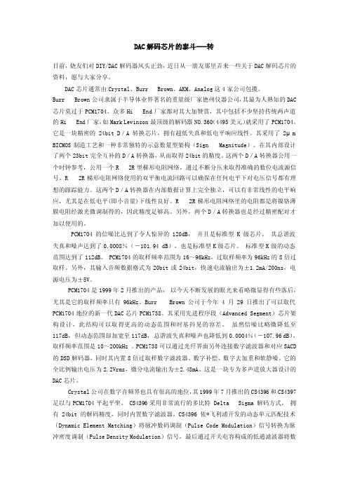
Daniel Beer dlbeer@ 8 Mar 2011
A common method of generating an analog output signal using a digital microcontroller is to filter a pulse-width modulated digital output. A pulse-width modulator is usually implemented in hardware by having a counter run freely, with triggers set to turn off the output when the counter rolls overflows its maximum value, and turn on when the counter reaches the software-set threshold value.
Qint(t) = integral{0, t} Q(t)
PDM seeks to minimze Qint(t)at each step, or to at least hold it within a small bounded range. A simple algorithm for this is:
/* Sine table. 256 entries representing one complete cycle. The signal * is scaled so that it fits the range representable with an 8-bit * unsigned integer. */
PDM is a method of continuously varying the average value of a digital signal, but without having a fixed modulation period, as in PWM. Here's an example that shows a single cycle of a sine wave rendered as a digital signal using PDM:
Most microcontrollers have hardware built-in to do this, but when it's not available, it can be done in software. Y ou have an interrupt called at the same frequency as the hardware counter would have counted, implement the same logic using a threshold and a counter variable, and switch the output pin on and off accordingly. T he only problem with this is the computing resources used - an 8-bit PWM would require 256 counts per PWM cycle. If you were to produce an output signal at the modest sampling rate of 1 kHz, you'd need to handle 256,000 interrupts per second - quite a lot of work for a small microcontroller.
This table is small enough to fit into most microcontrollers' ROMs, and is scaled and shifted to make PDM easier. The actual formula used to generate the above table is: