sop k013 event order and information collection Chn
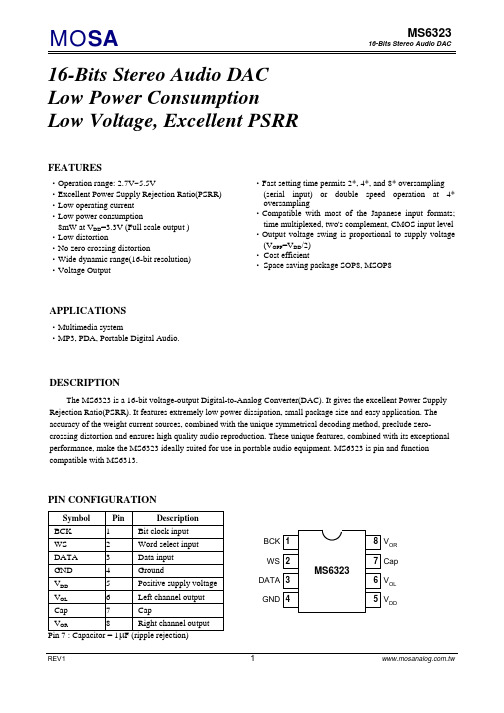
MS6323中文资料
3.3V ELECTRICAL CHARACTERISTICS
(Ta=25 Symbol DC Characteristics VCAP VDC VFS IQ PSRR CS Res THD+N S/N Voltage at CAP Output DC level Full scale output voltage Quiescent current Power supply rejection ratio Channel separation Resolution Total harmonic distortion plus noise Signal-to-noise ratio VFS=0.5VDD At code 0000H CAP=1uF, f=100Hz CAP=10uF, f=100Hz 1.60 1.60 1.5 45 63 78 86 1.65 1.65 1.65 2.0 50 68 84 -66 0.05 92 1.70 1.70 1.8 2.3 16 -62 0.08 V V Vpp mA dB dB dB bits dB , VDD=3.3V, VSS=0V, f=1kHz, Cap=1uF; unless otherwise specified) Parameter Conditions Min Typ Max Unit
4
元器件交易网
MOSA
TIMING AND DATA FORMAT
REFERENCE SOURCE
1uF VREF 4 GND
WS
2 CONTROL & TIMING
RIGHT INPUT LATCH 10uF 0.1uF
DATA
3
5
VDD
Fig.1
Discovering episodes with compact minimal windows-DMKD
ISUP信令消息参数
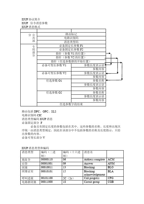
ISUP协议简介ISUP 信令消息参数路由包括 DPC、OPC、SLS电路识别码 CIC消息类型编码 ISUP消息必备固定部分 F必备且有固定长度的参数包括在其中。
这些参数的名称、长度和出现次序统一由消息类型规定,因此在该部分中不包括参数的名称及长度指示,只给出参数的内容。
必备可变长部分VISUP的参数名与编码ISUP参数详细编码1 接入转交信息Access delivery information2 接入转送Access transport1 . n消息单元的编码见 Q.931/$4.53自动拥塞级Automatic congestion level4 后向呼叫表示语Backward call indicators1 2Figure 7/Q.763 –后向呼叫表示语参数字段5呼叫变更消息 Call diversion informationFigure 8/Q.763 –呼叫变更消息参数字段在呼叫变更信息参数字段中使用一下编码6呼叫历史消息参考传播时延计数器的参数格式7 呼叫参数 Call reference (national use)123456Figure 9/Q.763 –呼叫参考参数字段在呼叫参考参数字段中,各字段使用一下编码:a) Call identity 呼叫标识用二进制表示的编码表示分配给呼叫的识别号码b) Signalling point code 信令点编码信令点的编码,呼叫标识语该编码有关8 被叫用户号码 Called party number123..nFigure 10/Q.763 –被叫用户号码参数字段在被叫用户号码参数字段中,各个字段使用以下编码:a) Odd/even indicator奇偶表示语0 地址信号为偶数1 地址信号为奇数b) Nature of address indicator地址性质表示语c) Internal Network Number indicator (INN ind.)内部网号码表示语(INN B表示语)0 允许选路到内部网号码1 不允许选路到内部网号码d) Numbering plan indicator/编号计划表示语0 0 0 备用0 0 1 ISDN(电话)编号计划 (参考 E.164)0 1 0 备用0 1 1 数据编号计划 (参考 X.121) (national use)1 0 0 用户电报编号计划 (参考 F.69) (national use)1 0 1 留作国内用1 1 0 留作国内用1 1 1 备用e) Address signal/地址信号0 0 0 0 digit 00 0 0 1 digit 10 0 1 0 digit 20 0 1 1 digit 30 1 0 0 digit 40 1 0 1 digit 50 1 1 0 digit 60 1 1 1 digit 71 0 0 0 digit 81 0 0 1 digit 91 0 1 0 spare1 0 1 1 code 111 1 0 0 code 121 1 0 1 spare1 1 1 0 spare1 1 1 1 STThe most significant address signal is sent first. Subsequent address signals are sent in successive 4-bit fields.f) Filler/填充码如果地址为奇数,则在最后一个地址信号后插入填充码 0000 。
MAXIM DS1090 说明书

General DescriptionThe DS1090 is a low-cost, dithered oscillator intended to be used as an external clock for switched-mode power supplies and other low-frequency applications.The dithering or sweeping function reduces peak-radi-ated emissions from the power supply at its fundamen-tal frequency, as well as harmonic frequencies. The device consists of a resistor-programmed master oscil-lator, factory-programmed clock prescaler, and a pin-programmed dither circuit. These features allow the DS1090 to be used in applications where a spread-spectrum clock is desired to reduce radiated emis-sions. A combination of factory-set prescalers and external resistor allows for output frequencies ranging from 125kHz to 8MHz. Both dither frequency and dither percentage are set using control pins.ApplicationsSwitched-Mode Power Supplies Servers PrintersEmbedded Microcontrollers Industrial Controls Automotive ApplicationsFeatures♦Low-Cost, Spread-Spectrum EconOscillator™♦Simple User Programming♦Output Frequency Programmable from 125kHz to 8MHz♦Dither Percentage Programmable from 0% to 8%♦Dither Rate Programmable (f MOSC / 512, 1024,2048, or 4096 )♦3.0V to 5.5V Single-Supply Operation ♦CMOS/TTL-Compatible Output♦Operating Temperature Range: -40°C to +85°CDS1090Low-Frequency, Spread-SpectrumEconOscillator______________________________________________Maxim Integrated Products1Pin ConfigurationOrdering InformationTypical Operating CircuitRev 1; 2/07For pricing, delivery, and ordering information,please contact Maxim/Dallas Direct!at 1-888-629-4642, or visit Maxim’s website at .Add “T” for Tape & Reel orders.EconOscillator is a trademark of Dallas Semiconductor.D S 1090Low-Frequency, Spread-Spectrum EconOscillator 2_____________________________________________________________________ABSOLUTE MAXIMUM RATINGSRECOMMENDED DC OPERATING CONDITIONSDC ELECTRICAL CHARACTERISTICS(V CC = +3.0V to +5.5V, T A = -40°C to +85°C, unless otherwise noted.)Stresses beyond those listed under “Absolute Maximum Ratings” may cause permanent damage to the device. These are stress ratings only, and functional operation of the device at these or any other conditions beyond those indicated in the operational sections of the specifications is not implied. Exposure to absolute maximum rating conditions for extended periods may affect device reliability.Voltage Range on V CC Relative to Ground...........-0.5V to +6.0V Voltage Range on Input PinsRelative to Ground.................................-0.5V to (V CC + 0.5V),not to exceed 6.0VOperating Temperature Range ...........................-40°C to +85°C Storage Temperature Range.............................-55°C to +125°C Soldering Temperature.......................................See IPC/JEDECJ-STD-020A SpecificationDS1090Low-Frequency, Spread-SpectrumEconOscillator_____________________________________________________________________3AC ELECTRICAL CHARACTERISTICSNote 2:This is the change observed in output frequency due to changes in temperature or voltage.Note 3:See the Typical Operating Characteristics section.Note 4:Parameter is guaranteed by design and is not production tested.Note 5:This is a percentage of the output period. Parameter is characterized but not production tested. This can be varied from 0% to 8%.Note 6:This indicates the time between power-up and the outputs becoming active. An on-chip delay is intentionally introduced to allow the oscillator to stabilize. t STAB is equivalent to ~500 clock cycles and is dependent upon the programmed output frequency.Note 7:Output voltage swings can be impaired at high frequencies combined with high output loading.D S 1090Low-Frequency, Spread-Spectrum EconOscillator 4_____________________________________________________________________Typical Operating Characteristics(V CC = +3.3V, T A = +25°C, unless otherwise noted.)SUPPLY CURRENT vs. SUPPLY VOLTAGESUPPLY VOLTAGE (V)S U P P L Y C U R R E N T (m A )5.04.54.03.50.951.201.451.700.703.05.5SUPPLY CURRENT vs. TEMPERATURETEMPERATURE (°C)S U P P L Y C U R R E N T (m A )603510-150.700.901.101.301.500.50-4085SUPPLY CURRENT vs. OUTPUT LOADINGLOAD CAPACITANCE (pF)S U P P L Y C U R R E N T (m A )35302520151012340540OUTPUT VOLTAGE HIGH vs. OUTPUT CURRENTOUTPUT CURRENT (mA)O U T P U T V O L T A G E(V )-1-2-3-42.82.93.03.12.7-5OUTPUT VOLTAGE LOW vs. OUTPUT CURRENTOUTPUT CURRENT (mA)O U T P U T V O L T A G E (V )43210.10.20.30.4005OUTPUT FREQUENCY vs. SUPPLY VOLTAGESUPPLY VOLTAGE (V)F R E Q U E N C Y (M H z )5.04.54.03.5567891043.05.5DS1090Low-Frequency, Spread-SpectrumEconOscillator_____________________________________________________________________5OUTPUT FREQUENCY vs. TEMPERATURETEMPERATURE (°C)F R E Q U E N C Y (M H z )603510-1556789104-4085DUTY CYCLE vs. TEMPERATURETEMPERATURE (°C)D U T Y C Y C LE (%)603510-154950515248-4085RESISTOR CURRENT vs. RESISTOR VALUER SET (k Ω)R E S I S T O R C U R R E N T (μA )706050101214161884080FREQUENCY ERRORvs. SUPPLY VOLTAGE (FROM 3.3V)SUPPLY VOLTAGE (V)F R E Q U E N C Y E R R O R (%)5.04.54.03.5-2.502.55.0-5.03.05.5FREQUENCY ERRORvs. TEMPERATURE (FROM +25°C)TEMPERATURE (°C)F R E Q U E N C Y E R R O R (%)603510-15-1.01.02.0-2.0-4085POWER SPECTRUM vs. SPREADFREQUENCY (MHz)P O W E R (d B m )5.35-70-60-50-40-30-20-100-804.805.90Typical Operating Characteristics (continued)(V CC = +3.3V, T A = +25°C, unless otherwise noted.)D S 1090Low-Frequency, Spread-Spectrum EconOscillator 6_____________________________________________________________________Pin DescriptionBlock DiagramDS1090Low-Frequency, Spread-SpectrumEconOscillatorDetailed DescriptionThe DS1090 is a center-dithered, spread-spectrum sili-con oscillator for use as an external clock in reduced-EMI applications. With a combination of factory-programmed prescalers and a user-selected external resistor, output frequencies from 125kH z to 8MH z can be achieved. The output center frequency can be dithered by selecting the desired dither rate and ampli-tude with discrete inputs J0, J1, JC0, and JC1.The DS1090 contains four basic circuit blocks: master oscillator, factory-programmed prescaler, dither gener-ator, and the voltage-bias circuit that provides the feed-back path to the master oscillator for frequency control and dithering functions.Master OscillatorThe master oscillator is programmable in the applica-tion by the use of an external resistor (R SET ) tied to ground (GND). Resistor values of 45k Ωto 91k Ωvary the square-wave output frequency of the voltage-con-trolled master oscillator (f MOSC ) from 8MH z down to 4MHz (see Figure 1).The master oscillator (Hz) frequency can be stated asFactory-Programmed PrescalerThe prescaler divides the frequency of the master oscil-lator by 1, 2, 4, 8, 16, or 32 to generate the square-wave output clock (f OSC ). This divisor is factory-set and is an ordering option.Dither GeneratorSpread-spectrum functionality is achieved by a user-configurable divider (determines dither rate), a triangle generator, and a user-configurable dither amplitude cir-cuit (see Block Diagram ).The input to the triangle-wave generator is derived from the internal master oscillator and is fed through a user-configurable divider. The settings of control pins JC0and JC1 determine this dither rate divisor setting (see Table 1), dividing the master clock by 4, 8, 16, or 32.The clock signal is further divided by 128 in the triangle-wave generator, which results in a triangle-wave signal of either 1/512th, 1/1024th, 1/2048th, or 1/4096th of the master oscillator (f MOD ), depending upon the user’s divisor setting.The dithering frequency can be also expressed as the result ofwhere Divisor is 4, 8, 16, or 32.Figure 1. Master Oscillator FrequencyFigure 2. Center Frequency Dither DiagramTable 1. Dither Rate Divisor SettingsD S 1090Low-Frequency, Spread-Spectrum EconOscillator Maxim cannot assume responsibility for use of any circuitry other than circuitry entirely embodied in a Maxim product. No circuit patent licenses are implied. Maxim reserves the right to change the circuitry and specifications without notice at any time.8_____________________Maxim Integrated Products, 120 San Gabriel Drive, Sunnyvale, CA 94086 408-737-7600©2007 Maxim Integrated Productsis a registered trademark of Maxim Integrated Products.is a registered trademark of Dallas Semiconductor Corporation.Dither amplitude (measured in percent ±from the mas-ter oscillator center frequency) is set using input pins J0 and J1. This circuit uses a sense current from the master oscillator bias circuit to adjust the amplitude ofthe triangle-wave signal to a voltage level that modu-lates the master oscillator to a percentage of its resis-tor-set center frequency. This percentage is set in theend application to be 0%, 2%, 4%, or 8% (see Table 2).Application InformationPin ConnectionThe DS1090 is intended to provide a fixed-frequency,dithered clock to be used as a clock driver for DC-DC converters and other applications requiring a low-frequency EMI-reduced clock oscillator. All control pins must be biased per Tables 1 and 2 for proper operation for the individual application’s requirements. R SET must be tied to ground (GND) by a customer-supplied resistor.R SET Resistor SelectionThe value of the resistor used to select the desired fre-quency is calculated using the formula in the Master Oscillator section (see also Figure 1). It is recommended to use, at minimum, a 1%-tolerance, 1/16th-watt compo-nent with a temperature coefficient that satisfies the over-all stability requirements desired of the end-equipment.Place the external R SET resistor as close as possible to minimize lead inductance.Power-Supply DecouplingTo achieve best results, it is highly recommended that a decoupling capacitor is used on the IC power-supply pins. Typical values of decoupling capacitors are 0.01µF and 0.1µF. Use a high-quality, ceramic, surface-mount capacitor, and mount it as close as possible to the V CC and GND pins of the IC to minimize lead inductance.。
A3报告培训教材

解决问题型A3 建议型A3 状况型A3
12/7/2015
Aleris Restricted & Confidential
2
A3的优点
结构化思考
PDCA,帮助员工深 刻理解并掌握问题解决方法,实践 于工作中。
凝练问题
把握问题的本质,用一 张A3纸即可清晰明了地展现问题解决 整体“过程 ”。
沟通平台
A3 报告培训教材
Dec 2015
12/7/2015
Aleris Restricted & Confidential
1
什么是A3
A3报告(A3 Report)是一种由丰田公司开创的方法,通常用 图形把问题、分析、改正措施、以及执行计划囊括在一张大的 (A3)纸上。
在丰田公司,A3报告已经成为一个标准方法,用来总结解决 问题的方案,进行状态报告,以及绘制价值流图。 A3分类: - Problem solving A3 - Proposal A3 - Status A3
● ● ●
▲ ● ▲ ● ▲ ● ▲
● ● ●
△預計完成時間 ▲實際完成時間
○ 符合目標 △優良目標
×出現問題
12/7/2015
Aleris Restricted & Confidential
11
7.检查/确认效果
努力地理解问题发生的因果关系,不要仅仅实施一些使问题消失的的方法
要验证方案总体的有效性 使用与目标设置中的相同标准 选定验证有效性的方法,尽量逐一实施 预先计划要收集的数据 明确数据的收集人和收集的频次
4. Actions follow up
Item Objectives # 1.1 1 Heat up factor opetimazation 1.2 1.3 High Level Action Additional data processing in order to compare the various tests Compare the recent TUS test results Wu Yin Arrange additional heat up factor trials based on the current results and the discussion outcome Evaluation of the 6061 test results-check BT calculation Preparation of 7075 trials within the next campaigns -Go on test Pre trial with an empty furnace for segment 1-4 fan speed to 90%-SAT Heat up factor test in order to evaluate the fan speed effect for the heat up factor, energy consumption and temperature accuracy Tracking of the “growing plate effect” at the exit door light barrier and after the quench section-Xiqun check how the program calculate length Tracking of the actual safety distance at the kick out position Take a picture of every deviating plate group at the end of the roller table and record the plate positions by the operators Registration of every event causing any kind of scrap ( even partial scrap) with all relevant data and counter measures (like the 2nd annealing file). Incl. later scrapings at the stretcher, CT testing or inspection. Registration of every event causing or could cause any kind of scrap, 2nd annealing or standstill. With the relevant data, root cause, short time actions and long time actions. Align with the 2nd annealing and scrap file Improvement of the issue reporting form. Needs to be filled in with proper information's by production and maintenance.- meeting with Mike&frank Development of temp mitigation activities for all issues which can’t be solved immediately. Communication via controlled documents to all relevant production or maintenance employees Sales training in order to raise the awareness for this issue. Integrate Dave in this process. Consequent loading of every possible combination. Loading preparation by pre-stacking of batches Can combinations be better supported (annealing time tolerances? Stronger quench code?) -Test plan review next week Sufficient number of qualified operators available Manning pattern ideal? Shift improvements (best practice) Pre treatment of the plates (Cleaning, sorting, stacking) Are based on the so far collected cases general activities defined? Pareto? Adjustment of the max load volume according the annealing temperature-trail for 5000mm2 to verify heat up capbility(prepare the plate)-Libing provide demension 470C, 475C, 480C 4400mm2 (4200mm2) 495C 4200mm2 530C, 535C 4000mm2-4200 mm2 for all Need to find the balance between delivery dates and throughput. Consequent “thick to thin “ and “long to short” campaigns Simulation of the planned sequences and alternatives up front Consequent combination of all kind of tasks at the furnace. Various maintenance departments, QA, Production. Should be covered by a detailed maintenance planner schedule. Collect the pipeline activities continuously Change of the current practice – edge trim the head and the tail according to the BT Plate length optimization (the shorter the better) Fast unloading tool for the transportation plates and test plates or cooling down of the test plates in the quench-try in next TUS Can the SAT be carried out with a partially emptied furnace Zhang Libing Zhang Libing Pang Liang Wu Yin Pang Liang Frank Sun Responsible Start Finish Mar date date W13 3/25 3/25 3/25 3/25 3/25 3/25 3/25 3/25 3/25 3/25 5/20 5/15 4/30 Done Done Done 5/13 5/29 On going. 4/10 5/3 Apr
【建立】1X和DO主被叫信令流程

【关键字】建立1.MS主叫流程MS主叫流程图如下所示。
Airbridge用户接口跟踪主叫信令流程:MS主叫流程说明如下:具体流程如下:1.MS在空中接口的接入信道上向BSS发送Origination Message(起呼消息),并要求BSS应答。
2.BSS收到Origination Message(起呼消息)后向MS发送BS Ack Order(基站证实指令)。
3.BSS构造CM Service Request(业务请求消息)消息,封装后发送给MSC。
对于需要电路交换的呼叫,BSS可以在该消息中推荐所需地面电路,并请求MSC分配该电路。
4.MSC向BSS发送Assignment Request(指配请求消息)消息,请求分配无线资源。
如果MSC能够指配BSS在CM Service Request消息中推荐的地面电路,那么MSC将在Assignment Request消息中指配该地面电路。
否则将指配其他地面电路。
5.BSS为MS分配业务信道后,在寻呼信道上发送Channel Assignment Message或Extended Channel Assignment Message(扩展信道指配消息),开始建立无线业务信道。
6.MS在指定的反向业务信道上发送Traffic Channel preamble (TCH Preamble)。
7.BSS捕获反向业务信道后,在前向业务信道上发送BS Ack Order(基站证实),并要求MS应答。
8.MS在反向业务信道上发送MS Ack Order(移动台证实),应答BSS的BS Ack Order。
9.BSS向MS发送Service Connect Message(业务连接消息)或Service Option ResponseOrder(业务响应指令),以指定用于呼叫的业务配置。
10.MS收到Service Connect Message或Service Option Response Order后,开始根据指定的业务配置处理业务,并以Service Connect Completion Message(业务连接完成消息)作为响应。
CIP-013-2 —— 电子产品供应链风险管理指南说明书

A.Introduction1.Title: Cyber Security - Supply Chain Risk Management2.Number: CIP-013-23.Purpose: To mitigate cyber security risks to the reliable operation of the BulkElectric System (BES) by implementing security controls for supply chain riskmanagement of BES Cyber Systems.4.Applicability:4.1.Functional Entities: For the purpose of the requirements contained herein, thefollowing list of functional entities will be collectively referred to as “ResponsibleEntities.” For requirements in this standard where a specific functional entity orsubset of functional entities are the applicable entity or entities, the functionalentity or entities are specified explicitly.4.1.1.Balancing Authority4.1.2.Distribution Provider that owns one or more of the following Facilities,systems, and equipment for the protection or restoration of the BES:4.1.2.1.Each underfrequency Load shedding (UFLS) or undervoltageLoad shedding (UVLS) system that:4.1.2.1.1.Is part of a Load shedding program that is subject toone or more requirements in a NERC or RegionalReliability Standard; and4.1.2.1.2.Performs automatic Load shedding under a commoncontrol system owned by the Responsible Entity,without human operator initiation, of 300 MW ormore.4.1.2.2.Each Remedial Action Scheme (RAS) where the RAS is subject toone or more requirements in a NERC or Regional ReliabilityStandard.4.1.2.3.Each Protection System (excluding UFLS and UVLS) that appliesto Transmission where the Protection System is subject to oneor more requirements in a NERC or Regional ReliabilityStandard.4.1.3.Generator Operator4.1.4.Generator Owner4.1.5.Reliability Coordinator4.1.6.Transmission Operator4.1.7.Transmission Owner4.2.Facilities:For the purpose of the requirements contained herein, the followingFacilities, systems, and equipment owned by each Responsible Entity in 4.1above are those to which these requirements are applicable. For requirements in this standard where a specific type of Facilities, system, or equipment or subset of Facilities, systems, and equipment are applicable, these are specifiedexplicitly.4.2.1.Distribution Provider: One or more of the following Facilities, systemsand equipment owned by the Distribution Provider for the protection orrestoration of the BES:4.2.1.1.Each UFLS or UVLS System that:4.2.1.1.1.Is part of a Load shedding program that is subject toone or more requirements in a NERC or RegionalReliability Standard; and4.2.1.1.2.Performs automatic Load shedding under a commoncontrol system owned by the Responsible Entity,without human operator initiation, of 300 MW ormore.4.2.1.2.Each RAS where the RAS is subject to one or more requirementsin a NERC or Regional Reliability Standard.4.2.1.3.Each Protection System (excluding UFLS and UVLS) that appliesto Transmission where the Protection System is subject to oneor more requirements in a NERC or Regional ReliabilityStandard.4.2.1.4.Each Cranking Path and group of Elements meeting the initialswitching requirements from a Blackstart Resource up to andincluding the first interconnection point of the starting stationservice of the next generation unit(s) to be started.4.2.2.Responsible Entities listed in 4.1 other than Distribution Providers: AllBES Facilities.4.2.3.Exemptions: The following are exempt from Standard CIP-013-2:4.2.3.1.Cyber Assets at Facilities regulated by the Canadian NuclearSafety Commission.4.2.3.2.Cyber Assets associated with communication networks and datacommunication links between discrete Electronic SecurityPerimeters (ESPs).4.2.3.3.The systems, structures, and components that are regulated bythe Nuclear Regulatory Commission under a cyber security planpursuant to 10 C.F.R. Section 73.54.4.2.3.4.For Distribution Providers, the systems and equipment that arenot included in section 4.2.1 above.4.2.3.5.Responsible Entities that identify that they have no BES CyberSystems categorized as high impact or medium impactaccording to the identification and categorization processrequired by CIP-002 or any subsequent version of that ReliabilityStandard.5.Effective Date:See Implementation Plan for Project 2019-03.B.Requirements and MeasuresR1.Each Responsible Entity shall develop one or more documented supply chain cyber security risk management plan(s) for high and medium impact BES Cyber Systems andtheir associated Electronic Access Control or Monitoring Systems (EACMS) and PhysicalAccess Control Systems (PACS). The plan(s) shall include: [Violation Risk Factor:Medium] [Time Horizon: Operations Planning]1.1.One or more process(es) used in planning for the procurement of BES CyberSystems and their associated EACMS and PACS to identify and assess cybersecurity risk(s) to the Bulk Electric System from vendor products or servicesresulting from: (i) procuring and installing vendor equipment and software; and(ii) transitions from one vendor(s) to another vendor(s).1.2.One or more process(es) used in procuring BES Cyber Systems, and theirassociated EACMS and PACS, that address the following, as applicable:1.2.1.Notification by the vendor of vendor-identified incidents related to theproducts or services provided to the Responsible Entity that pose cybersecurity risk to the Responsible Entity;1.2.2.Coordination of responses to vendor-identified incidents related to theproducts or services provided to the Responsible Entity that pose cybersecurity risk to the Responsible Entity;1.2.3.Notification by vendors when remote or onsite access should no longerbe granted to vendor representatives;1.2.4.Disclosure by vendors of known vulnerabilities related to the products orservices provided to the Responsible Entity;1.2.5.Verification of software integrity and authenticity of all software andpatches provided by the vendor for use in the BES Cyber System and theirassociated EACMS and PACS; and1.2.6.Coordination of controls for vendor-initiated remote access.M1.Evidence shall include one or more documented supply chain cyber security risk management plan(s) as specified in the Requirement.R2.Each Responsible Entity shall implement its supply chain cyber security risk management plan(s) specified in Requirement R1. [Violation Risk Factor: Medium][Time Horizon: Operations Planning]Note: Implementation of the plan does not require the Responsible Entity torenegotiate or abrogate existing contracts (including amendments to masteragreements and purchase orders). Additionally, the following issues are beyond thescope of Requirement R2: (1) the actual terms and conditions of a procurementcontract; and (2) vendor performance and adherence to a contract.M2.Evidence shall include documentation to demonstrate implementation of the supply chain cyber security risk management plan(s), which could include, but is not limited to, correspondence, policy documents, or working documents that demonstrate use of the supply chain cyber security risk management plan.R3.Each Responsible Entity shall review and obtain CIP Senior Manager or delegate approval of its supply chain cyber security risk management plan(s) specified inRequirement R1 at least once every 15 calendar months. [Violation Risk Factor:Medium] [Time Horizon: Operations Planning]M3.Evidence shall include the dated supply chain cyber security risk management plan(s) approved by the CIP Senior Manager or delegate(s) and additional evidence todemonstrate review of the supply chain cyber security risk management plan(s).Evidence may include, but is not limited to, policy documents, revision history,records of review, or workflow evidence from a document management system that indicate review of supply chain risk management plan(s) at least once every 15calendar months; and documented approval by the CIP Senior Manager or delegate.pliancepliance Monitoring Processpliance Enforcement Authority:“Compliance Enforcement Authority” (CEA) means NERC or the Regional Entity,or any entity as otherwise designated by an Applicable Governmental Authority,in their respective roles of monitoring and/or enforcing compliance withmandatory and enforceable Reliability Standards in their respectivejurisdictions.1.2.Evidence Retention:The following evidence retention period(s) identify the period of time an entityis required to retain specific evidence to demonstrate compliance. For instanceswhere the evidence retention period specified below is shorter than the timesince the last audit, the CEA may ask an entity to provide other evidence toshow that it was compliant for the full time period since the last audit.The Responsible Entity shall keep data or evidence to show compliance asidentified below unless directed by its CEA to retain specific evidence for alonger period of time as part of an investigation.•Each Responsible Entity shall retain evidence of each requirement in this standard for three calendar years.•If a Responsible Entity is found non-compliant, it shall keep informationrelated to the non-compliance until mitigation is complete and approved orfor the time specified above, whichever is longer.•The CEA shall keep the last audit records and all requested and submitted subsequent audit records.pliance Monitoring and Enforcement ProgramAs defined in the NERC Rules of Procedure, “Compliance Monitoring andEnforcement Program” refers to the identification of the processes that will beused to evaluate data or information for the purpose of assessing performanceor outcomes with the associated Reliability Standard.Version History1 07/20/17 Respond to FERC OrderNo. 829.1 08/10/17 Approved by the NERCBoard of Trustees.1 10/18/18 FERC Order approvingCIP-013-1. Docket No.RM17-13-000.Revised2 08/01/2019 Modified to addressdirective in FERC OrderNo. 850.2 11/05/2020 Approved by the NERCBoard of Trustees.2 3/18/2021 FERC Order approvingCIP-013-2.Docket No.RD21-2-000.2 4/5/2021 Effective Date 10/1/2022。
Ovation I O Reference Manual

This publication adds the Eight Channel RTD module to the Ovation I/O Reference Manual. It should be placed between Sections 19 and 20.Date: 04/03IPU No.243Ovation ® Interim Publication UpdatePUBLICATION TITLEOvation I/O Reference ManualPublication No. R3-1150Revision 3, March 2003Section 19A. Eight Channel RTDModule19A-1. DescriptionThe Eight (8) channel RTD module is used to convert inputs from Resistance Temperature Detectors (RTDs) to digital data. The digitized data is transmitted to the Controller.19A-2. Module Groups19A-2.1. Electronics ModulesThere is one Electronics module group for the 8 channel RTD Module:n5X00119G01 converts inputs for all ranges and is compatible only with Personality module 5X00121G01 (not applicable for CE Mark certified systems).19A-2.2. Personality ModulesThere is one Personality module groups for the 8 channel RTD Module:n5X00121G01 converts inputs for all ranges and is compatible only with Electronics module 5x00119G01 (not applicable for CE Mark certified systems).19A-2.3. Module Block Diagram and Field Connection WiringDiagramThe Ovation 8 Channel RTD module consists of two modules an electronics module contains a logic printed circuit board (LIA) and a printed circuit board (FTD). The electronics module is used in conjunction with a personalty module, which contains a single printed circuit board (PTD). The block diagram for the 8 channel RTD moduleis shown in Figure 19A-1.Table 19A-1. 8 Channel RTD Module Subsystem ChannelsElectronic Module Personality Module85X00119G015X00121G01Figure 19A-1. 8 Channel RTD Module Block Diagram and Field Connection Wiring Diagram19A-3. SpecificationsElectronics Module (5X00119)Personality Module (5X00121)Table 19A-2. 8 Channel RTD Module SpecificationsDescription ValueNumber of channels8Sampling rate50 HZ mode: 16.67/sec. normally. In 3 wire mode, leadresistance measurement occurs once every 6.45 sec.during which the rate drops to 3/sec.60 HZ mode: 20/sec. normally. In 3 wire mode, leadresistance measurement occurs once every 6.45 sec.during which the rate drops to 2/sec.Self Calibration Mode: Occurs on demand only. The ratedrops to 1/sec. once during each self calibration cycle.RTD ranges Refer to Table 19A-3.Resolution12 bitsGuaranteed accuracy (@25°C)0.10% ±[0.045 (Rcold/Rspan)]% ± [((Rcold + Rspan)/4096 OHM)]% ± [0.5 OHM/Rspan]% ±10 m V ± 1/2LSBwhere:Rcold and Rspan are in Ohms.Temperature coefficient 10ppm/°CDielectric isolation:Channel to channel Channel to logic 200V AC/DC 1000 V AC/DCInput impedance100 M OHM50 K OHM in power downModule power 3.6 W typical; 4.2 W maximumOperating temperature range0 to 60°C (32°F to 140°F)Storage temperature range-40°C to 85°C (-40°F to 185°F)Humidity (non-condensing)0 to 95%Self Calibration On Demand by Ovation ControllerCommon Mode Rejection120 dB @ DC and nominal power line frequency+/- 1/2%Normal Mode Rejection100 dB @ DC and nominal power line frequency+/- 1/2%Table 19A-3. 8 Channel RTD RangesScale #(HEX)Wires Type Tempo FTempo CRcold(ohm)Rhot(ohm)Excitationcurrent(ma)Accuracy± ±countsAccuracy± ±% ofSPAN1310OhmPL0 to1200–18 t o6496106.3 1.090.222310OhmCU 0 to302–18 t o1508.516.5 1.0 130.32D350OhmCU 32 to2840 to1405080 1.0110.2711350OhmCU 32 to2300 to1105378 1.0120.30193100Ohm PL –4 to334–16 t o16892163.671.0110.27223100Ohm PL 32 to5200 to269100200 1.0100.25233100Ohm PL 32 to10400 to561100301 1.0100.25253120Ohm NI –12 t o464–11 t o240109360 1.0100.25263120Ohm NI 32 to1500 to70120170 1.0130.32283120Ohm NI 32 to2780 to122120225 1.0110.27804100Ohm PL 32 to5440 to290100 208 1.0100.25814100Ohm PL 356 t o446180 t o230168 186 1.0300.74824200Ohm PL 32 to6980 to370200 473 1.0120.30834200Ohm PL 514 t o648268 t o342402452 1.0290.71844100Ohm PL 32 to1240 to51100120 1.0190.47854100Ohm PL 32 to2170 to103100 140 1.0130.3286 4100Ohm PL 32 to4120 to211100 180 1.0110.27874100Ohm PL 32 to7140 to379100 240 1.0100.25884120Ohm PL 511 t o662266 t o350200230 1.0240.5919A-4. 8 Channel RTD Terminal Block Wiring Information19A-4.1. Systems Using Personality Module 5X00121G01 Each Personality module has a simplified wiring diagram label on its side, which appears above the terminal block. This diagram indicates how the wiring from the field is to beconnected to the terminal block in the base unit. The following table lists and defines the abbreviations used in this diagram.Table 19A-4. Abbreviations Used in the DiagramAbbreviation Definition+IN, -IN Positive and negative sense input connectionEarth ground terminal. Used for landing shields when the shield is to begrounded at the module.PS+, PS-Auxiliary power supply terminals.RTN Return for current source connection.SH Shield connector. used for landing shields when the shield is to begrounded at the RTD.SRC Current source connection.Note:PS+ and PS- are not used by this module.19A-5. 8 Channel RTD Module Address Locations19A-5.1. Configuration and Status RegisterWord address 13 (D in Hex) is used for both module configuration and module status. The Module Status Register has both status and diagnostic information. The bit information contained within these words is shown in Table 19A-5.Definitions for the Configuration/Module Status Register bits:Bit 0:This bit configures the module (write) or indicates the configuration state of the module (read). A “1” indicates that the module is configured. Note that until the module is configured, reading from addresses #0 through #11 (B in Hex) will produce an attention status.Bit 1:This bit (write “1”) forces the module into the error state, resulting in the error LED being lit. The read of bit “1” indicates that there is an internal module error,or the controller has forced the module into the error state. The state of this bit is always reflected by the module’s Internal Error LED. Whenever this bit is set,an attention status is returned to the controller when address #0 through #11(B in Hex) are read.Table 19A-5. 8 Channel RTD Configuration/Status Register (Address 13 0xD in Hex)Bit Data Description -Configuration Register (Write)Data Description -Status Register (Read)0Configure Module Module Configured(1 = configured; 0 = unconfigured)1Force errorInternal or forced error(1 = forced error; 0 = no forced error)250/60 Hz select (0 = 60Hz, 1 = 50Hz)50/60 Hz System (1 = 50Hz) d(read back)3SELF_CAL (Initiates Self Calibration)Warming bit (set during power up or configuration)40050060Module Not Calibrated 708CH.1 _ 3/4 Wire.CH.1 _ 3/4 Wire - Configuration (read back)9CH.2 _ 3/4 Wire.CH.2 _ 3/4 Wire - Configuration (read back)10CH.3 _ 3/4 Wire.CH.3 _ 3/4 Wire - Configuration (read back)11CH.4 _ 3/4 Wire.CH.4 _ 3/4 Wire - Configuration (read back)12CH.5 _ 3/4 Wire.CH.5 _ 3/4 Wire - Configuration (read back)13CH.6 _ 3/4 Wire.CH.6 _ 3/4 Wire - Configuration (read back)14CH.7 _ 3/4 Wire.CH.7 _ 3/4 Wire - Configuration (read back)15CH.8 _ 3/4 Wire.CH.8 _ 3/4 Wire - Configuration (read back)Bit 2:The status of this bit (read) indicates the conversion rate of the module, write to this bit configures the conversion rate of A/D converters as shown below.see Table 19A-6.Bit3:Write: This bit is used to initiate self-calibration. Read: This bit indicates that the module is in the “Warming” state. this state exists after power up and ter-minates after 8.16 seconds. the module will be in the error condition during the warm up period.Bit4 & 5:These bits are not used and read as “0” under normal operation.Bit 6:This bit (read) is the result of a checksum test of the EEPROM. A failure of this test can indicate a bad EEPROM, but it typically indicates that the module has not been calibrated. A “0” indicates that there is no error condition. If an error is present, the internal error LED is lit and attention status will be returned for all address offsets 0-11 (0x0 - 0xB). The “1” state of this bit indicates an unre-coverable error condition in the field.Bit 7:This bits is not used and read as “0” under normal operation.Bit 8 - 15:These bits are used to configure channels 1 - 8 respectively for 3 or 4 wire op-eration. A “0” indicates 3 wire and a “1” indicates 4 wire operation, see Table 19A-7 and Table 19A-8).Word address 12 (0xC) is used to configure the appropriate scales for Channels 1 - 4 (refer to Table 19A-7 and Table 19A-8).Table 19A-6. Conversion Rate Conversion Rate (1/sec.)Bit 260 (for 60Hz systems)050 (for 50Hz systems)1Table 19A-7. Data Format for the Channel Scale Configuration Register(0xC)Bit Data Description Configuration (Write)Data Description Status (Read)0 Configure Channel #1scale - Bit 0Channel #1 scale configuration (read back) - Bit 01Configure Channel #1scale - Bit 1Channel #1 scale configuration (read back) - Bit 12Configure Channel #1scale - Bit 2Channel #1 scale configuration (read back) - Bit 23Configure Channel #1scale - Bit 3Channel #1 scale configuration (read back) - Bit 34Configure Channel #2 scale - Bit 0Channel #2 scale configuration (read back) - Bit 05Configure Channel #2 scale - Bit 1Channel #2 scale configuration (read back) - Bit 16Configure Channel #2 scale - Bit 2Channel #2 scale configuration (read back) - Bit 27Configure Channel #2 scale - Bit 3Channel #2 scale configuration (read back) - Bit 38Configure Channel #3 scale - Bit 0Channel #3 scale configuration (read back) - Bit 09Configure Channel #3 scale - Bit 1Channel #3 scale configuration (read back) - Bit 1Caution:Configuring any or all channel scales while the system is running will cause all channels to return attention status for up to two seconds following the reconfiguration.Caution:Configuring any or all channel scales while the system is running will cause all channels to return attention status for up to two seconds following the reconfiguration.10Configure Channel #3 scale - Bit 2Channel #3 scale configuration (read back) - Bit 211Configure Channel #3 scale - Bit 3Channel #3 scale configuration (read back) - Bit 312Configure Channel #4 scale - Bit 0Channel #4 scale configuration (read back) - Bit 013Configure Channel #4 scale - Bit 1Channel #4 scale configuration (read back) - Bit 114Configure Channel #4 scale - Bit 2Channel #4 scale configuration (read back) - Bit 215Configure Channel #4 scale - Bit 3Channel #4 scale configuration (read back) - Bit 3Table 19A-8. Data Format for the Channel Scale Configuration Register(0xE)Bit Data Description Configuration (Write)Data Description Status (Read)0 Configure Channel #5 scale - Bit 0Channel #5 scale configuration (read back) - Bit 01Configure Channel #5 scale - Bit 1Channel #5 scale configuration (read back) - Bit 12Configure Channel #5 scale - Bit 2Channel #5 scale configuration (read back) - Bit 23Configure Channel #5 scale - Bit 3Channel #5 scale configuration (read back) - Bit 34Configure Channel #6 scale - Bit 0Channel #6 scale configuration (read back) - Bit 05Configure Channel #6 scale - Bit 1Channel #6 scale configuration (read back) - Bit 16Configure Channel #6 scale - Bit 2Channel #6 scale configuration (read back) - Bit 27Configure Channel #6 scale - Bit 3Channel #6 scale configuration (read back) - Bit 38Configure Channel #7 scale - Bit 0Channel #7 scale configuration (read back) - Bit 09Configure Channel #7 scale - Bit 1Channel #7 scale configuration (read back) - Bit 110Configure Channel #7 scale - Bit 2Channel #7 scale configuration (read back) - Bit 211Configure Channel #7 scale - Bit 3Channel #7 scale configuration (read back) - Bit 312Configure Channel #8 scale - Bit 0Channel #8 scale configuration (read back) - Bit 013Configure Channel #8 scale - Bit 1Channel #8 scale configuration (read back) - Bit 114Configure Channel #8 scale - Bit 2Channel #8 scale configuration (read back) - Bit 215Configure Channel #8 scale - Bit 3Channel #8 scale configuration (read back) - Bit 3Table 19A-7. Data Format for the Channel Scale Configuration Register(0xC)19A-6. Diagnostic LEDsTable 19A-9. 8 Channel RTD Diagnostic LEDsLED DescriptionP (Green)Power OK LED. Lit when the +5V power is OK.C (Green)Communications OK LED. Lit when the Controller is communicatingwith the module.I (Red)Internal Fault LED. Lit whenever there is any type of error with themodule except to a loss of power. Possible causes are:n - Module initialization is in progress.n - I/O Bus time-out has occurred.n - Register, static RAM, or FLASH checksum error.n - Module resetn - Module is uncalibrated.n - Forced error has been received from the Controllern - Communication between the Field and Logic boards failedCH1 - CH 8 (Red)Channel error. Lit whenever there is an error associated with a channel or channels. Possible causes are:n - Positive overrangen - Negative overrangen Communication with the channel has failed。