dc compact model
海洋显示和计算器MC-5150-AC DC x86 ECDIS电脑说明书

MC-5150-AC/DCThe MC-5150-AC/DC computers feature the Intel ® Core ™ i5 520E processor and come with 4 serial ports, 2 Gigabit Ethernet ports, 6 USB hosts, and 8 NMEA ports. The computers offer high performance and versatile peripherals for marine applications.Designed with highest quality and durability in mind, the marine-grade MC-5150-AC/DC computers feature a rugged chassis proven against 1G anti-vibration, providing a most reliable platform even in harshenvironments. In addition, the compact size, fanless design, and low power consumption deliver an optimal thermal solution, making installations easy for bridge systems in marine ers can easily install Windows XP Embedded, XP Professional, or Windows 7 for a flexible and friendly system development and user environment.AC/DC Model Front ViewOverviewAppearanceLPT PortPorts x 2 (type A)(Power, Storage)AC Model Rear ViewDC Model Rear ViewSpecificationsKeyboard DVI-I/VGA(DC 24V)Keyboard DVI-I/VGA ComputerCPU: Intel® Core™ i5-520E (BGA CPU package), dual core threaded 64 bit 2.4 GHz processorOS: Windows 7, Windows XP SP3, Windows XP Embedded (must be installed by the user)System Chipset: Intel® QM57 Express Chipset FSB: 1066System Memory: 8 GB capacity, 2 GB pre-installed: 2 slots 4 GB DDR3-1066 204 pin SO-DIMM SDRAM USB: USB 2.0 hosts x 6, Type A connectors Storage:• 1 internal SATA storage tray• 1 removable SATA storage drive trayOther PeripheralsAudio: line-in/out interfaceKB/MS: 2 PS/2 interfaces supporting standard PS/2 keyboard and mouseDisplayDisplay Interface:• VGA Interface: 15-pin D-Sub connector (female), with resolution up to 1920 x 1080• DVI-I Interface: 29-pin DVI-I connector (female)Graphics Controller: Onboard Intel® HD graphicsEthernet Interface LAN: 2 auto-sensing 10/100/1000 Mbps ports (RJ45)Magnetic Isolation Protection: 1.5 KV built inSerial InterfaceSerial Standards:• 2 RS-232/422/485 ports, software-selectable (DB9 male) • 2 RS-232 ports (DB9)• 8 NMEA ports (Phoenix 3.81 mm compatible connector)Serial Communication ParametersData Bits: 5, 6, 7, 8Stop Bits: 1, 1.5, 2Parity: None, Even, Odd, Space, MarkFlow Control: RTS/CTS, XON/XOFF, ADDC® (automatic data direction control) for RS-485Baudrate: 50 bps to 230.4 KbpsSerial SignalsRS-232: TxD, RxD, DTR, DSR, RTS, CTS, DCD, GND RS-422: TxD+, TxD-, RxD+, RxD-, GND RS-485-4w: TxD+, TxD-, RxD+, RxD-, GND RS-485-2w: Data+, Data-, GNDLEDsSystem: Storage, PowerLAN: 100M/Link x 2, 1000M/Link x 2 (on connector)Physical CharacteristicsHousing: Aluminum, sheet metal Weight: 6.85 kg Dimensions:• Without ears: 287 x 250 x 135 mm (11.30 x 9.84 x 5.31 in) • With ears: 287 x 290 x 140 mm (11.30 x 11.42 x 5.51 in)Mounting: WallEnvironmental LimitsOperating Temperature: -15 to 55°C (5 to 131°F)Storage Temperature: -20 to 60°C (-4 to 131°F)Ambient Relative Humidity: 5 to 95% (non-condensing)Anti-Vibration:•***********(ClassA),sinewave,2-100Hz,1Oct./min.,1.5hr per axis•************,randomwave,3-100Hz,2.5hrperaxis•***********(ClassC),sinewave,2-50Hz,1Oct./min.,1.5hr per axisPower RequirementsInput Voltage:• DC Model: 24 VDC (with tolerance from 18 to 30 VDC, 2-pin terminal block)• AC Model: 100 to 240 VACPower Consumption: Less than 100 W, 2.5 A @ 24 VDCStandards and CertificationsSafety: UL 60950-1, DNV 2.4, IEC 60945 (4th), IACS E10, CCC (GB4943, GB9254, GB17625.1)EMC: EN 55032 Class B, EN 55024, FCC Part 15 Subpart B Class B Marine: IEC 60945 4th, IACS E10Green Product: RoHS, cRoHS, WEEEReliability MTBF (mean time between failures): 220,490 hrs WarrantyWarranty Period: 3 yearsDetails: See /warrantyOrdering InformationAvailable ModelsMC-5150-AC: x86-based ECDIS computer with Intel® Core™ i5 CPU processor, 4 serial ports, 8 NMEA ports, 2 Gigabit Ethernet ports, 6 USB hosts, storage, VGA/DVI, and AC power input MC-5150-DC: x86-based ECDIS computer with Intel® Core™ i5 CPU processor, 4 serial ports, 8 NMEA ports, 2 Gigabit Ethernet ports, 6 USB hosts, storage, VGA/DVI, and DC power input Optional Accessories (for AC models only, can be purchased separately) PWC-C13US-3B-183: Power cord with 3-pin connector, USA plugPWC-C13EU-3B-183: Power cord with 3-pin connector, Euro plugPWC-C13UK-3B-183: Power cord with 3-pin connector, British plugPWC-C13AU-3B-183: Power cord with 3-pin connector, Australia plugPWC-C13CN-3B-183: Power cord with 3-pin connector, China plug Package Checklist• MC-5150 computer• 2 removable storage protection keys• 8 screws for internal and removable HDD• Terminal block for power input (DC model only)• 8 terminal blocks for NMEA ports• Documentation and driver CD• Quick installation guide (printed)• Warranty card。
Tenma数字控制可编程DC电源模型72-2535、72-2540、72-2545、72-2550和

TMDigital-Control and Programmable DC Power Supply Models: 72-2535, 72-2540, 72-2545, 72-2550 & 72-10480User Manual TMSafety SymbolsT his chapter contains important safety instructions that you must follow when operating the Tenma power supply and when keeping it in storage. Read the following before any operation to insure your safety and to keep the best condition for the Tenma power supply.Safety SymbolsThese safety symbols may appear in this manual or on the series.WARNINGDANGER High Voltage.Earth (ground) TerminalSafety InstructionSafety GuidelinesDo not block or obstruct the cooling fan vent opening.Avoid severe impacts or rough handling that leads to damage.Do not discharge static electricity. Do not disassemble unless you are qualified as service personnel.AC InputAC Input Voltage : 110V / 120V / 220V / 230V , 50 / 60HzConnect the protective grounding conduct or of the AC power cord to an earth ground, to avoid electrical shock.Operation EnvironmentLocation: Indoor, no direct sunlight, dust free, almost non-conductive pollution (note below)Relative Humidity: < 80%Altitude: < 2000mTemperature: 0-40°CStorage environmentLocation: IndoorRelative Humidity: < 70%Temperature: -10-70°C TMFuseModel110/ 120V220 /230V72-10480T4A/ 250V T2A/ 250V72-2535T5A/ 250V T3A/ 250V72-2540T5A/ 250V T3A/ 250V72-2545T5A/ 250V T3A/ 250V72-2550T5A/250T3A/250V To ensure fire protection, replace the fuse only with the specified type and rating.Disconnect the power cord before fuse replacement. Make sure the cause of fuse blowout is fixed before fuse replacement. Series Lineup/Main FeaturesModel V Meter A Meter USB Resolution72-10480 4 digit 4 digit No10mV/1mA72-2535 4 digit 4 digit Yes10mV/1mA72-2540 4 digit 4 digit Yes10mV/1mA72-2545 4 digit 4 digit Yes10mV/1mA72-2550 4 digit 4 digit Yes10mV/1mAPerformanceLow noise: cooling fan controlled by heat sink temperatureCompact size, light weightOperationConstant voltage / constant current operationDigital panel control4 pairs of panel setup save / recall Coarse and fine Voltage / Current controlSoftware calibrationBeep outputKey lock functionProtectionOverload protectionReverse polarity protectionInterfacesUSB/RS 232 for remote control (only for 72-2535, 72-2540, 72-2545, 72-2550) TMFront Panel OverviewDisplayVoltage level VVoltmeter displays the setup value of output voltage.Current level A Displays the setup value of output current.Condition IndicationOVP O VP is the indicator of over voltage protection. When over voltage function is turned on, OVP indicator lights on; when output voltage is higher than protection setup value due to unexpected conditions, output cuts off and OVP indicator flick -ers; Press the key OVP again, and the power supply recovers. OCP O CP is OCP indicator. When over current function is turned on, OCP indicator lights on. C.CC.C is constant current indicator. When power supply is in the mode of constant current, this light is on. C.VC.V is constant voltage indicator. When power supply is in the mode of constant voltage, this light is on. OUTOUT is output indicator. If light on, there is voltage output in the output terminal.Storage IndicationIndication of saving and recalling 5 setups stored internally. TMBrief Introduction of Panel OperationSaves or recalls panel settings. For settings, 1 ~ 4 are available. For save / recall details, see Page 08.Front panel lock_out function. For details, see Page 07Over-Current protect on/off, Pressing this key for more than 2 seconds will make beep On/OFF.Over-voltage Protect On/OffOutput On/Off.Voltage-Current Setting AdjustmentDigit Selector ButtonsThen turn the key ADJUST and the settings of the setted voltage or current can be adjusted.On / Off main power. For power up sequence, see Page 06Outputs voltage and current.Connects the ground (earth) terminal. TMRS232 dependent interface based on remote control order (see Page 08) ; only for KAXXXXP series, such as KA3003P and soon.RS232 dependent interface based on remote control order (see Page 08); only for KAXXXXP series, such as KA3003P and so on.The power cord socket mainly accepts AC values: 115V / 230V, 50 / 60 Hz. Please refer to the fuse parameters on the back fuse label to replace the specified fuse.Make sure the correct type of fuse is installed before power upOperationConnect AC power cordC onnecting AC power cord and selecting the corresponding AC voltage accordingto the back label on voltage; then connecting the AC power cord to the socket on the back panel PoweronP ress the power switch to turn power on. The display initializes, showing themodel of the ma chine and then showing the setting last. Power offP ress the power switch again to turn power off. TMOutput On / OffPanel OperationP ress the Output button to turn on output; and the button LED also turns on. Press ing the Output button again to turn off the output and the LED.Note: I f there are any of the following conditions, the output will automatically turn off.1. OVP turns on and there are unusual OVP on the output terminal.2. The setting voltage is more than that of the OVP.3. Recalling other se tups from the memory.Beep On / OffPanel OperationB y default, the beep sound is enabled. To turn off the beep, press the OCP (BEEP) button for 2 se co nds. A beep comesout and the beep setting will be turned off . To enable the beep, press the OCP (BEEP) button again for 2 seconds.Front Panel LockPanel operationP ress the LOCK button to lock the front panel button operation. The LED turns on. To unlock, press the LOCK button for 2 seconds.Output SetPanel operation1. Connecting the load to the front port, red ( +), black (-).2. Setting output voltage and current.P ress the button Voltage/Current selection to switch voltage adjustment and current adjustment. Adjusting voltage and current with Voltage / Current Adjustment knob. By default, the Voltage and Current knob work in the coarse mode. To activate the fine mode, press the buttons to select the coarse mode or the fine mode.3. Turning on the output and press ing the output button. The button LED turns on and displays CV or CC mode.Save / Recall SetupSave SetupBack ground The front panel settings can be stored into one of the four internal memories.Contents T he following list shows the se tup contents:Fine / coarse knob editing modeBeep on / offOutput voltage / current levelThe following settings are always saved as “off “.Output on / offFront panel lock on / offPanel operation P ress one of the 4 buttons(M 1,M2,M3,M4) and the LED light turns on accordingly. After you adjust the value, it is saved automatically once it stops blinking.Recall Set upThe front panel settings can be recalled from one of the four internal memories. TMPress any button of M1 to M4, and take M1 for example; the memory of panel set tings is recalled in M1. After you recall M4, rot at e the shuttle knob and then M5 is recalled.It means the current memory is recalled that the memory indicator on the panel lights on accordingly.Note When a set ting is recalled, the out put automatically turns off.Remote ControlRemote Control SetupA ll the models 72-2535,72-2540,72-2545,72-2550 etc. can be connected to the PC through interfaces USB/RS232 on theback of the machine and controlled by the remote control.COM settingSet up the COM port inside the PC according to the following list.Baud rate: 9600Parity bit: NoneData bit: 8Stop bit: 1 Data flow control: NoneFunctionality checkRun this query command via the terminal application such as MTTTY (Multi-threaded TTY).*IDN? This should return the identification information: Manufacturer, model name, serial number. 72-10480 SN:xxxxxxxx Vx.xxRemote Control ProceduresEntering the Remote Control Mode1. Connecting USB2. The power supply will automatically connect. After normal connection, there will be a tweet from the power supply itself.3. The panel keys are locked, so the power supply can only rely on the remote control.Exiting from the Remote Control Mode1. Closing the remote control software.2. Disconnecting USB from the back.3. The power supply disconnects; a tweet from the beep with the hint that the remote control is over.4. The power supply automatically comes into the panel control mode. TMFAQQ1: The panel buttons don’t work when power on.A1: The panel is locked. Press the key for over 2 seconds, and then the panel will unlock.Q2: Pressing ON/OFF, there is no out put when power on.A2: Current set up is 0.Q3: Output voltage rises slowly when out put button is on.A3: Current set up is too small.Q4: Making OCP on and pressing out put switch; and then the out put is automatically shut off.A4: Current protection value set up is too small. You could press output switch and then make OCP on. SpecificationsNote: The specifications below are tested under the conditions of temperature 25°C ±5°C and the warm-up for 20 minutes.Models72-1048072-253572-254072-254572-2550 Voltage Range0-30V0-30V0-30V0-60V0-60V Current Range0-3A0-3A0-5A0-2A0-3A Load RegulationVoltage Current ≤0.01% +2mV≤0.1% +5mV≤0.01% +2mV≤0.1% +10mV≤0.01% +2mV≤0.1% +5mV≤0.01% +2mV≤0.1% +5mV≤0.01% +2mV≤0.1% +5mVLine RegulationVoltage Current ≤0.01% +3mV≤0.1% +3mV≤0.01% +3mV≤0.1% +3mV≤0.01% +3mV≤0.1% +3mV≤0.01% +3mV≤0.1% +3mV≤0.01% +3mV≤0.1% +3mVSetup ResolutionVoltage Current 10mV1mA10mV1mA10mV1mA10mV1mA10mV1mASetup Accuracy (25°C ±5°C)Voltage Current ≤0.5% +20mV≤0.5% +5mV≤0.5% +20mV≤0.5% +5mV≤0.5% +20mV≤0.5% +10mV≤0.5% +30mV≤0.5% +5mV≤0.5% +30mV≤0.5% +5mVRipple (20-20M)Voltage Current ≤1mVrms≤3mArms≤1mVrms≤3mArms≤2mVrms≤3mArms≤1mVrms≤3mArms≤1mVrms≤3mArmsTemp. CoefficientVoltage Current ≤150ppm≤150ppm≤150ppm≤150ppm≤150ppm≤150ppm≤150ppm≤150ppm≤150ppm≤150ppmRead Back AccuracyVoltage Current 10mV1mA10mV1mA10mV1mA10mV1mA10mV1mARead Back Temp. CoefficientVoltage Current ≤150ppm≤150ppm≤150ppm≤150ppm≤150ppm≤150ppm≤150ppm≤150ppm≤150ppm≤150ppmReaction TimeVoltage Rise Voltage Drop≤100mS≤100mS(10% Rated Load)≤100mS≤100mS(10% Rated Load)≤100mS≤100mS(10% Rated Load)≤100mS≤100mS(10% Rated Load)≤100mS≤100mS(10% Rated Load) TMImportant Notice : This data sheet and its contents (the “Information”) belong to the members of the Premier Farnell group of companies (the “Group”) or are licensed to it. No licence is granted for the use of it other than for information purposes in connection with the products to which it relates. No licence of any intellectual property rights is granted. The Information is subject to change without notice and replaces all data sheets previously supplied. The Information supplied is believed to be accurate but the Group assumes no responsibility for its accuracy or completeness, any error in or omission from it or for any use made of it. Users of this data sheet should check for themselves the Information and the suitability of the products for their purpose and not make any assumptions based on information included or omitted. Liability for loss or damage resulting from any reliance on the Information or use of it (including liability resulting from negligence or where the Group was aware of the possibility of such loss or damage arising) is excluded. This will not operate to limit or restrict the Group’s liability for death or personal injury resulting from its negligence. Tenma is the registered trademark of the Group. © Premier Farnell plc 2012.InterfaceOptional Interface (for programmable models only): RS232, USB AccessoriesUser manual 1PC; Power Cord: 1×UK power cord and 1×Euro power Cord Weight and Dimensions(mm)110(W) × 156(H) × 260(D), 72-10480/722535 × 3.6kg, 72-2540, 72-2545 × 4.3kg, 72-2550 × 4.8kg。
莫尔森DC DC转换器产品说明书
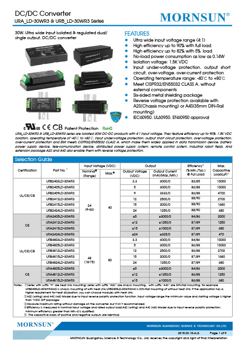
30W,Ultra wide input isolated ®ulated dual/single output,DC/DC converterCB Patent ProtectionRoHSFEATURES●Ultra wide input voltage range (4:1)●High efficiency up to 90%with full load ●High efficiency up to 82%with 5%load●No-load power consumption as low as 0.14W ●Isolation voltage:1.5K VDC●Input under-voltage protection,output short circuit,over-voltage,over-current protection ●Operating temperature range:-40℃to +80℃●Meet CISPR32/EN55032CLASS A,without external components●Six-sided metal shielding package●Reverse voltage protection available with A2S(Chassis mounting)or A4S(35mm DIN-Rail mounting)●IEC60950,UL60950,EN60950approvalURA_LD-30WR3&URB_LD-30WR3series are isolated 30W DC-DC products with 4:1input voltage.They feature efficiency up to 90%,1.5K VDC isolation,operating temperature of -40℃to +80℃,Input under-voltage protection,output short circuit protection,over-voltage protection,over-current protection and EMI meets CISPR32/EN55032CLASS A,which make them widely applied in data transmission device,battery power supply device,tele-comunication device,distributed power supply system,remote control system,industrial robot fields.And extension package A2S and A4S also enable them with reverse voltage protection.Product Characteristic CurveFig.1Apply model :URA2405LD-30W(H)R3(9-18V input voltage )、URA2424LD-30W(H)R3(9-18V input voltage )、URA4805LD-30W(H)R3(18-36V input voltage )Fig.2Apply model :URA2405LD-30W(H)R3(18-36V input voltage )、URA2424LD-30W(H)R3(18-36V input voltage )、URA4805LD-30W(H)R3(36-75V input voltage )、URA2412LD-30W(H)R3、URA2415LD-30W(H)R3、URA4812LD-30W(H)R3、URA4815LD-30W(H)R3Fig.3Apply model :URB2403LD-30W(H)R3、URB2405LD-30W(H)R3、URB4803LD-30W(H)R3、URB4805LD-30W(H)R3Fig.4Apply model :URB2409LD-30W(H)R3、URB2412LD-30W(H)R3、URB2415LD-30W(H)R3、URB2424LD-30W(H)R3、URB4812LD-30W(H)R3、URB4815LD-30W(H)R3、URB4824LD-30W(H)R3All the DC/DC converters of this series are tested according to the recommended circuit(see Fig.5)before delivery.If it is required to further reduce input and output ripple,properly increase the input&output of additional capacitors Cin and Cout or select capacitors of low equivalent impedance provided that the capacitance is no larger than the max.capacitive load of the product.V in0VV in0VDual outp ut:Single outputvoltage(VDC)Cout(µF)Cin(µF)Dual outputvoltage(VDC)Cout(µF)Cin(µF)3.3/5/9220100±5/±12/±1522010012/15/24100±241002.EMC solution-recommended circuitSingle outputFig.6Notes:Part①in the Fig.6is used for EMC test and part②for EMI filtering;selected based on needs.Parameter descriptionModel Vin:24V Vin:48VFUSEChoose according to actual inputcurrentMOV S20K30S14K60C0680µF/50V330µF/100VC1330µF/50V330µF/100VC2 4.7µF/50V 2.2µF/100VC3Refer to the Cout in Fig.5LCM1mH,recommended to useMORNSUN’s FL2D-30-102sCY1、CY21nF/2KVDual outputFig.7Notes:Part①in the Fig.7is used for EMC test and part②for EMI filtering;selected based on needs.Model Vin:24V Vin:48VFUSE Choose according to actual inputcurrentMOV S20K30S14K60C0680µF/50V330µF/100VC1 2.2µF/50V 2.2µF/100VC2 2.2µF/50V 2.2µF/100VC3330µF/50V330µF/100VC4Refer to the Cout in Fig.5LDM1 3.3µHCY1、CY2 2.2nF/400V AC Safety Y Capacitor3.Application of Trim and calculation of Trim resistanceTrim up Trim downApplied circuits of Trim(Part in broken line is the interior of models)Calculation formula of Trim resistance:up: a=VrefVo’-VrefR1R=TaR2R-a2-R3down: a=VrefVo’-VrefR2R=TaR1R-a1-R3R T is Trim resistance,a is a self-definedparameter,with no real meaning.Vo’for the actual needs of the up ordown regulated voltageVout(VDC)R1(KΩ)R2(KΩ)R3(KΩ)Vref(V)3.34.801 2.8712.4 1.245 2.883 2.8710 2.597.500 2.8715 2.51211.000 2.8715 2.51514.494 2.8715 2.52424.872 2.8717.8 2.54.It is not allowed to connect modules output in parallel to enlarge the power5.For more information please find DC-DC converter application notes on Horizontal Package(without heat sink)Dimensions and Recommended LayoutHorizontal Package(with heat sink)DimensionsURA_LD-30WR3A2S&URB_LD-30WR3A2S(without heat sink)DimensionsNotes:1.Packing information please refer to Product Packing Information which can be downloaded from .Horizontal Packing Bag Number:58200035(without heat sink),58200051(with heat sink),A2S/A4S Packing Bag Number:58220022;2.The maximum capacitive load offered were tested at input voltage range and full load;3.Unless otherwise specified,parameters in this datasheet were measured under the conditions of Ta=25℃,humidity<75%RH with nominalinput voltage and rated output load;4.All index testing methods in this datasheet are based on Company’s corporate standards;5.We can provide product customization service,please contact our technicians directly for specific information;6.Products are related to laws and regulations:see"Features"and"EMC";7.Our products shall be classified according to ISO14001and related environmental laws and regulations,and shall be handled byqualified units.Mornsun Guangzhou Science&Technology Co.,Ltd.Address:No.5,Kehui St.1,Kehui Development Center,Science Ave.,Guangzhou Science City,Luogang District,Guangzhou,P.R.China Tel:86-20-38601850-8801Fax:86-20-38601272E-mail:***************。
ECE60系列AC-DC电源模块说明说明书

Overvoltage Protection Overload Protection Short Circuit Protection Temperature Coefficient
General
Characteristic Efficiency Isolation Switching Frequency Power Density Mean Time Between Failure Weight
code ECE60 DIN CLIP. 4. Average of efficiencies measured at 25%, 50%, 75% & 100% load with 230 VAC input.
Summary
Characteristic Input Range
No Load Input Power Efficiency
2
ECE60 Series
AC-DC Power Supplies
EMC: Emissions
Phenomenon Conducted Radiated Harmonic Current Voltage Flicker
Standard
EN55032 EN55032 EN61000-3-2 EN61000-3-3
ECE60 Series
AC-DC Power Supplies
60 Watts
• Ultra Compact Size • Single Outputs from 3.3 to 48 V • Encapsulated • PCB & Chassis Mount Versions • <0.3 W No Load Input Power • -40 to +70 °C Operation • Peak Load Capability • 3 Year Warranty
Tripp Lite PowerVerter 700W Ultra-Compact Inverter

PowerVerter® 700W Ultra-Compact Inverter with 1 AC OutletMODEL NUMBER:PVX700DescriptionPower electrical appliances in your vehicle with Tripp Lite's PVX700 DC-to-AC power inverter. Converts 12 volt DC power from your automotive battery connection to modified sine wave AC power compatible with 220-240 volt/50Hz equipment. 700 watt continuous/1400 watt instantaneous peak surge power handling capability powers laptop computers, battery chargers, TV/VCRs, gaming systems and small power tools. Universal outlet accepts French, German and UK style connectors, plus a variety of other international plug sets. Rugged all-metal case withstands punishing environments. Compact design offer ample power capacity and weighs only 1.27 kg. Built-in low-battery alarm and auto-shutoff prevents deep battery discharge, ensuring that enough charge remains to start your vehicle. Includes lighted power switch, user replaceable fuse, built-in cooling fan.FeaturesConverts 12 volt DC to modified sine wave AC power compatible with 220-240 volt/50Hz equipmentqDC input terminals assure solid connection to battery with user-supplied cablesq700 watt continuous/1400 watt instantaneous peak surge power handling capability supports a variety of electronic loadsqUniversal outlet accepts French, German and UK style AC input connectors, plus a variety of other international plug setsqRugged all-metal caseqUltra compact, high-frequency inverter design weighs approximately 1.27 kgqLow input voltage alarm alerts users to low vehicle battery conditions starting at 10.5VqAutomatic low voltage shutoff prevents deep battery discharge starting at 10VqLighted power switch offers visual notification of power statusqOverload alarm/shutdown detects wattage overload on inverter outlets and shuts down inverter as a protective measureqBuilt-in cooling fan prevents overheating during extended usage periodsqIntegrated mounting feet provide secure, fixed installationqAttractive full-color retail packagingq Highlights12V DC input; 230V AC output;1 universal global outletq700 watts continuous outputqHardwire DC input terminalsqIncludes "battery saver" lowvoltage alarm/shutdownqPackage IncludesPVX700 DC-to-AC invertersystemqUser manual with warrantyinformationqSpecifications© 2023 Eaton. All Rights Reserved. Eaton is a registered trademark. All other trademarks are the property of their respective owners.。
Recom 6W AC DC 双输出电源说明书
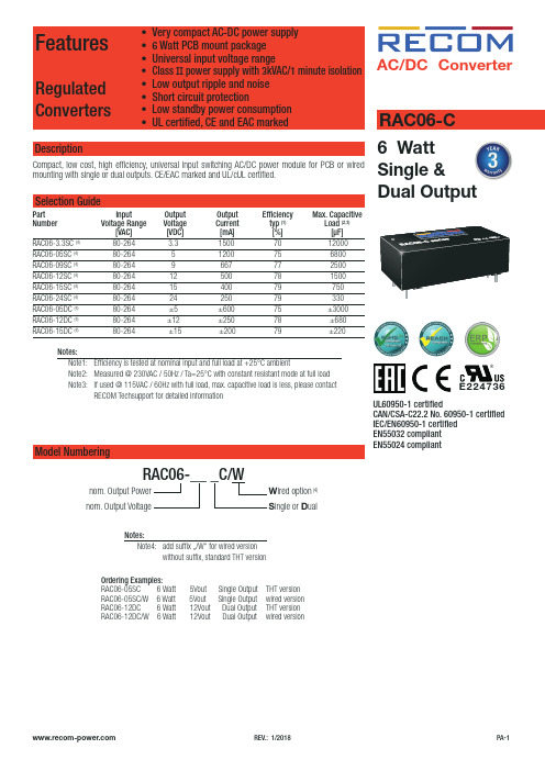
AC/DC Converer6 Watt Single &Dual OutputDescriptionCompact, low cost, high efficiency, universal input switching AC/DC power module for PCB or wired mounting with single or dual outputs. CE/EAC marked and UL/cUL certified.RAC06-CSelection GuidePart Input Output Output Efficiency Max. CapacitiveNumber Voltage Range Voltage Current typ (1) Load (2,3)[VAC] [VDC] [mA] [%] [µF]RAC06-3.3SC (4) 80-264 3.3 1500 70 12000RAC06-05SC (4)80-264 5 1200 75 6800RAC06-09SC (4) 80-264 9 667 77 2500RAC06-12SC (4)80-264 12 500 78 1500RAC06-15SC (4) 80-264 15 400 79 750RAC06-24SC (4)80-264 24 250 79 330RAC06-05DC (4) 80-264 ±5 ±600 75 ±3000RAC06-12DC (4) 80-264 ±12 ±250 78 ±680RAC06-15DC (4) 80-264 ±15 ±200 79 ±220Notes:Note4: add suffix …/W“ for wired version without suffix, standard THT version Model NumberingS ingle or D ualnom. Output Power nom. Output VoltageRAC06-__ _C/WW ired option (4)Notes:Note1: Efficiency is tested at nominal input and full load at +25°C ambientNote2: Measured @ 230VAC / 50Hz / Ta=25°C with constant resistant mode at full load Note3: If used @ 115VAC / 60Hz with full load, max. capacitive load is less, please contact RECOM Techsupport for detailed informationOrdering Examples:RAC06-05SC 6 Watt 5Vout Single Output THT version RAC06-05SC/W 6 Watt 5Vout Single Output wired version RAC06-12DC 6 Watt 12Vout Dual Output THT version RAC06-12DC/W 6 Watt 12Vout Dual Outputwired versionUL60950-1 certifiedCAN/CSA-C22.2 No. 60950-1 certified IEC/EN60950-1 certified EN55032 compliant EN55024 compliantE224736Specifications (measured at Ta= 25°C, full load otherwise noted)REGULATIONSParameter Condition Value Output Accuracy±2.0% max. Line Regulation low line to high line±0.3% typ. Load Regulation (7)5% to 100% load0.5% typ.Notes:Note7: Operation below 5% load will not harm the converter, but specifications may not be metSpecifications (measured at Ta= 25°C, full load otherwise noted)PROTECTIONSParameterTypeValueShort Circuit Protection (SCP)below 100m WHiccup mode, automatic recoveryOver Load Protection (OLP)115% - 145%Over Voltage Protection (OVP)zener diode clamp3.3Vout all others145% - 165%110% - 135%Over Voltage Category OVCII Isolation Voltage I/P to O/Ptested for 1 minute3kVACIsolation Resistance I/P to O/P1G W min.Isolation Capacitance 1000pF typ.Leakage Current0.85mA max.Notes:Note8: Refer to local safety regulations if input over-current protection is also required. Recommended fuse: slow blow typeENVIRONMENTALParameterConditionValueOperating Temperature Range (8)full load -25°C to +55°C refer to derating graph-25°C to +75°COperating Altitude 2000m Operating Humidity non-condensing95% RH max.Pollution Degree PD2MTBFaccording to MIL-HDBK-217F, G.B.+25°C +55°C>400 x 103 hours >200 x 103 hours-25-1052035506580110100806040907050302025100O u t p u t L o a d [%]957555701008060409070503020100O u t p u t L o a d [%]8090264Derating GraphLine DeratingSpecifications (measured at Ta= 25°C, full load otherwise noted)SAFETY AND CERTIFICATIONSCertificate Type (Safety)Report / File Number StandardInformation Technology Equipment - General Requirments for Safety E224736-A1-ULUL60950-1, 2nd Edition, 2007 CAN/CSA-C22.2 No. 60950-1-07, 2nd Edition, 2007Information Technology Equipment - General Requirments for Safety SPCLVD1605077-06IEC60950-1:2005 2nd Edition + A2:2013EN60950-1:2006 + A2:2013EAC Safety of Low Voltage Equipment RU-AT.AB37.B.02367TP TC 004/2011 RoHS2+RoHS-2011/65/EU + AM-2015/863EMC Compliance Condition Standard / Criterion Electromagnetic compatibility of multimedia equipment – Emission Requirements EN55032:2015 Information technology equipment - Immunity characteristics - Limits andmethods of measurementEN55024:2010 + A1:2015 ESD Electrostatic discharge immunity test Air ±8.0kV, Contact ±4.0kV IEC61000-4-2:2008, Criteria A Radiated, radio-frequency, electromagnetic field immunity test 3V/m IEC61000-4-3:2008, Criteria A Fast Transient and Burst Immunity AC Power Port: ±1.0kV IEC61000-4-4:2004, Criteria A Surge Immunity AC Power Port: L-N ±1.0kV IEC61000-4-5:2005, Criteria A Immunity to conducted disturbances, induced by radio-frequency fields AC Power Port 3.0V IEC61000-4-6:2008, Criteria A Power Magnetic Field Immunity50Hz, 1A/m IEC61000-4-8:2009, Criteria AVoltage Dips and InterruptionsVoltage Dips >95%Voltage Dips 30%Voltage Interruptions > 95%IEC61000-4-11:2004, Criteria AIEC61000-4-11:2004, Criteria AIEC61000-4-11:2004, Criteria BLimits of Harmonic Current Emissions EN61000-3-2:2014, Class A Limits of Voltage Fluctuations & Flicker EN61000-3-3:2013DIMENSION AND PHYSICAL CHARACTERISTICSParameter Type ValueMaterialcasepottingblack plastic (UL94V-0)epoxy (UL94V-0)Dimension (LxWxH)singledual50.9 x 25.5 x 16.4mm53.5 x 27.8 x 16.4mmWeight THT versionwired version35g typ.38g typ.Specifications (measured at Ta= 25°C, full load otherwise noted)Specifications (measured at Ta= 25°C, full load otherwise noted)The product information and specifications may be subject to changes even without prior written notice.The product has been designed for various applications; its suitability lies in the responsibility of each customer. The products are not authorized for use in safety-critical applications without RECOM’s explicit written consent. A safety-critical application is an application where a failure may reasonably be expected to endanger or cause PACKAGING INFORMATIONParameterTypeValuePackaging Dimension (LxWxH)tube cardboxTHT wired520.0 x 56.0 x 26.0520.0 x 195.0 x 67.0Packaging Quantity THT single THT dual wired10pcs 9pcs 20pcsStorage Temperature Range -40°C to +100°C Storage Humiditynon-condensing95% RH max.。
西门子PXCCompact系列控制器说明书
Technical Specification SheetDocument No. 149-454July 1, 2013 Siemens Industry, Inc. Page 1 of 8PXC Compact SeriesFigure 1. PXC Compact Series Controllers(PXC-24 and PXC-36 shown.)DescriptionThe PXC Compact Series (Programmable Controller–Compact) is a high-performance Direct Digital Control(DDC) supervisory equipment controller, which is anintegral part of the APOGEE® Automation System.The PXC Compact Series offers integrated I/O basedon state-of-the-art TX-I/O™ Technology, whichprovides superior flexibility of point and signal types,and makes it an optimal solution for Air Handling Unit(AHU) control. The PXC Compact operates stand-alone or networked to perform complex control,monitoring, and energy management functions withoutrelying on a higher-level processor.The PXC Compact Series communicates with otherfield panels or workstations on a peer-to-peerAutomation Level Network (ALN) and supports thefollowing communication options:∙ Ethernet TCP/IP∙P2 RS-485The PXC Compact is available with 16, 24, or 36 pointterminations. Selected models in the Compact Seriesprovide the following options:∙Support for FLN devices.∙An extended temperature range for the control ofrooftop devices.∙Support for Island Bus, which uses TX I/Omodules to expand the number of pointterminations.Features∙DIN rail mounted device with removable terminalblocks simplifies installation and servicing.∙Proven program sequences to match equipmentcontrol applications.∙Built-in energy management applications and DDCprograms for complete facility management.∙Comprehensive alarm management, historicaldata trend collection, operator control, andmonitoring functions.∙Sophisticated Adaptive Control, a closed loopcontrol algorithm that auto-adjusts to compensatefor load/seasonal changes.∙Message control for terminals, printers, pagers,and workstations.∙Highly configurable I/O using Siemens state-of-the-art TX-I/O™ Technology.∙HMI RS-232 port, which provides laptopconnectivity for local operation and engineering.∙Extended battery backup of Real Time Clock.∙Persistent database backup and restore within thecontroller.∙Optional HOA (Hand/Off/Auto) module forswappable and configurable HOA capability.∙Optional extended temperature range for rooftop installation.∙Optional peer-to-peer communications over industry-standard 10Base-T/100Base-TX Ethernet networks.∙Optional support for FLN devices.∙Optional support for P1 Wireless FLN.∙Optional operation as a P1 FLN device with default applications.∙Optional support for Virtual AEM.∙PXM10T and PXM10S support: Optional LCD Local user interface with HOA (Hand-off-auto)capability and point commanding and monitoringfeatures.The Compact SeriesIn addition to building and system management functions, the Compact Series includes several styles of controllers that flexibly meet application needs.PXC-16The PXC-16 provides control of 16 points, including 8 software-configurable universal points.Point count includes: 3 Universal Input (UI), 5 Universal I/O (U), 2 Digital Input (DI), 3 Analog Output (AOV), and 3 Digital Output (DO).PXC-24The PXC-24 provides control of 24 points, including 16 software-configurable universal points.Point count includes: 3 Universal Input (UI), 9 Universal I/O (U), 4 Super Universal I/O (X), 3 Analog Output (AOV), 5 Digital Output (DO).PXC-36The PXC-36 provides control of 36 local points, including 24 software-configurable universal points. Point count includes: 18 Universal I/O (U), 6 Super Universal I/O (X), 4 Digital Input (DI), and 8 Digital Output (DO).The PXC-36 offers the flexibility of expanding the total point count through a self-forming island bus. With the addition of a TX-I/O Power Supply, up to 4 TX-I/O modules can be supported. For more information, see the TX-I/O Product Range Technical Specification Sheet (149-476). Available OptionsThe following options are available to match the application:Ethernet or RS-485 ALNSupport for APOGEE P2 ALN through TCP/IP orRS-485 networks.FLN Support∙The PXC-24 “F32” models support up to 32 P1 FLN devices when the ALN is connected toTCP/IP.∙The PXC-24 “F” models with an FLN license support up to 32 P1 FLN devices when the ALN isconnected to TCP/IP.∙The PXC-36 with an FLN license supports up to 96 P1 FLN devices when the ALN is connected toRS-485 or TCP/IP.∙ A Wireless FLN may also be used to replace the traditional P1 FLN cabling with wirelesscommunication links that form a wireless meshnetwork. Additional hardware is required toimplement the Wireless FLN.For more information about FLN support, contact your local Siemens Industry representative.P1 FLN OperationThe PXC-16 and PXC-24 can be configured as a programmable P1 FLN device. In the P1 FLN mode, the PXC Compact functions as an equipment controller with customized programming and default applications.Virtual AEM SupportThe Virtual AEM license allows the PXC Compact to connect an RS-485 APOGEE Automation Level Network or individual field panels to a P2 Ethernet network without additional hardware.Extended Temperature OperationThe "R" models of the PXC Compact Series support extended temperature operation, allowing for rooftop installations.Field Panel GOThe PXC-36 supports Field Panel GO.The Field Panel GO license provides a Web-based user interface for your APOGEE® Building Automation System. It is an ideal solution for small or remote facilities with field panels on an Ethernet Automation Level Network (ALN).Page 2 of 8 Siemens Industry, Inc.HardwareThe PXC Compact Series consists of the following major components:∙ Input/Output Points∙ Power Supply∙ Controller ProcessorInput/Output Points∙The PXC Compact input/output points perform A/D or D/A conversion, signal processing, pointcommand output, and communication with thecontroller processor. The terminal blocks areremovable for easy termination of field wiring.∙The Universal and Super Universal points leverage TX-I/O™ Technology from SiemensIndustry to configure an extensive variety of pointtypes.∙Universal Input (UI) and Universal Input/Output (U) points are software-selectable to be:- 0-10V input-4-20 mA input- Digital Input-Pulse Accumulator inputs-1K Ni RTD @ 32°F (Siemens, JohnsonControls, DIN Standard)-1K Pt RTD (375 or 385 alpha) @ 32°F-10K NTC Thermistor (Type 2 and Type 3) @ 77°F-100K NTC Thermistor (Type 2) @ 77°F-0-10V Analog Output (Universal Input/Output (U) points only)∙Super Universal (X) points (PXC-24 and PXC-36 only) are software-selectable to be:- 0-10V input-4-20 mA input- Digital Input-Pulse Accumulator inputs-1K Ni RTD @ 32°F (Siemens, JohnsonControls, DIN Standard)-1K Pt RTD (375 or 385 alpha) @ 32°F-10K NTC Thermistor (Type 2 and Type 3) @ 77°F-100K NTC Thermistor (Type 2) @ 77°F- 0-10V Analog Output-4-20 mA Analog Output-Digital Output (using external relay)∙Dedicated Digital Input (DI) points (PXC-16 and PXC-36 only) are dry contact status sensing. ∙Digital Output (DO) points are 110/220V 4 Amp (resistive) Form C relays; LEDs indicate the status of each point.∙All PXC Compact Series models support 0-10 Vdc Voltage Analog Output circuits.∙On PXC-24 and PXC-36 models, the Super Universal circuits may be defined as 4-20 mAcurrent AO.Power Supply∙The 24 volt DC power supply provides regulated power to the input/output points and activesensors. The power supply is internal to the PXCCompact housing, eliminating the need forexternal power supply and simplifying installationand troubleshooting.∙The power supply works with the processor to ensure smooth power up and power downsequences for the equipment controlled by the I/O points, even through brownout conditions. Controller Processor∙The PXC Compact Series includes amicroprocessor-based multi-tasking platform forprogram execution and communications with theI/O points and with other PXC Compacts and field panels over the ALN.∙ A Human Machine Interface (HMI) port, with a quick-connect phone jack (RJ-45), uses RS-232protocol to support operator devices (such as alocal user interface or simple CRT terminal), and a phone modem for dial-in service capability.∙ A USB Device port supports a generic serial interface for an HMI or Tool connection.∙The program and database information stored in the PXC Compact RAM memory is battery-backed. This eliminates the need for time-consuming program and database re-entry in theevent of an extended power failure.∙The firmware, which includes the operating system, is stored in non-volatile flash ROMmemory; this enables firmware upgrades in thefield.∙Brownout protection and power recovery circuitry protect the controller board from powerfluctuations.∙LEDs provide instant visual indication of overall operation, network communication, and lowbattery warning.Siemens Industry, Inc. Page 3 of 8Programmable Control with Application FlexibilityThe PXC Compact Series of high performance controllers provides complete flexibility, which allows the owner to customize each controller with the exact program for the application.The control program for each PXC Compact is customized to exactly match the application. Proven Powers Process Control Language (PPCL), a text-based programming structure like BASIC, provides direct digital control and energy management sequences to precisely control equipment and optimize energy usage.Global Information AccessThe HMI port supports operator devices, such as a local user interface or simple CRT terminal, and a phone modem for dial-in service capability. Devices connected to the operator terminal port gain global information access.Multiple Operator AccessMultiple operators can access the network simultaneously. Multiple operator access ensures that alarms are reported to an alarm printer while an operator accesses information from a local terminal. When using the Ethernet TCP/IP ALN option, multiple operators may also access the controller through concurrent Telnet sessions and/or local operator terminal ports.Menu Prompted, English Language Operator InterfaceThe PXC Compact field panel includes a simple, yet powerful, menu-driven English Language Operator Interface that provides, among other things:∙Point monitoring and display∙ Point commanding∙Historical trend collection and display for multiple points∙ Event scheduling∙Program editing and modification via Powers Process Control Language (PPCL)∙Alarm reporting and acknowledgment∙Continual display of dynamic information Built-in Direct Digital Control RoutinesThe PXC Compact provides stand-alone Direct Digital Control (DDC) to deliver precise HVAC control and comprehensive information about system operation. The controller receives information from sensors in the building, processes the information, and directly controls the equipment. The following functions are available:∙Adaptive Control, an auto-adjusting closed loop control algorithm, which provides more efficient,adaptive, robust, fast, and stable control than thetraditional PID control algorithm. It is superior interms of response time and holding steady state,and at minimizing error, oscillations, and actuatorrepositioning.∙Closed Loop Proportional, Integral and Derivative (PID) control.∙ Logical sequencing.∙Alarm detection and reporting.∙ Reset schedules.Built-in Energy Management ApplicationsThe following applications are programmed in the PXC Compact Series and require simple parameter input for implementation:∙Automatic Daylight Saving Time switchover∙ Calendar-based scheduling∙ Duty cycling∙ Economizer control∙Equipment scheduling, optimization andsequencing∙ Event scheduling∙ Holiday scheduling∙Night setback control∙Peak Demand Limiting (PDL)∙Start-Stop Time Optimization (SSTO)∙ Temperature-compensated duty cycling∙Temporary schedule overridePage 4 of 8 Siemens Industry, Inc.SpecificationsDimensions (L × W × D)PXC-16 and PXC-2410.7 in. × 5.9 in. × 2.45 in. (272 mm × 150 mm × 62 mm)PXC-3611.5 in. × 5.9 in. × 3.0 in. (293 mm × 150 mm × 77 mm) Processor, Battery, and MemoryProcessor and Clock SpeedPXC-16 and PXC-24: Motorola MPC852T, 100 MHzPXC-36: Motorola MPC885, 133 MHz MemoryPXC-16 and PXC-24: 24 MB (16 MB SDRAM, 8 MB Flash ROM)PXC-36: 80 MB (64 MB SDRAM, 16 MB Flash ROM) Battery backup of Synchronous Dynamic (SD) RAM (field replaceable)Non-rooftop Models: 60 days (accumulated),AA (LR6) 1.5 Volt Alkaline (non-rechargeable)Rooftop (Extended Temperature) Models: 90 days (accumulated),AA (LR6) 3.6 Volt Lithium (non-rechargeable) Battery backup of Real Time ClockNon-rooftop Models: 10 yearsRooftop (Extended Temperature) Models: 18 months CommunicationA/D Resolution (analog in)16 bitsD/A Resolution (analog out)10 bitsEthernet/IP Automation Level Network (ALN)10Base-T or 100Base-TX compliant RS-485 Automation Level Network (ALN)1200 bps to 115.2 Kbps RS-485 P1 Field Level Network (FLN) on selected models, license required4800 bps to 38.4 Kbps Human-Machine Interface (HMI)RS-232 compliant, 1200 bps to 115.2 Kbps USB Device port (for non-smoke control applications only)Standard 1.1 and 2.0 USB device port, Type B female connector.USB Host port on selected models (for ancillary smoke control applications only)Standard 1.1 and 2.0 USB host port, Type A female connector. ElectricalPower Requirements24 Vac ±20% input @ 50/60 HzPower Consumption (Maximum)PXC-16: 18 VA @ 24 VacPXC-24: 20 VA @ 24 VacPXC-36: 35 VA @ 24 Vac Siemens Industry, Inc. Page 5 of 8AC Power and Digital OutputsNEC Class 1 Power Limited Communication and all other I/ONEC Class 2 Digital InputContact Closure SensingDry Contact/Potential Free inputs onlyDoes not support counter inputs Digital OutputClass 1 Relay Analog Output0 to 10 VdcUniversal Input (UI) and Universal Input/Output (U)Analog InputVoltage (0-10 Vdc)Current (4-20 mA)1K Ni RTD @ 32°F1K Pt RTD (375 or 385 alpha) @ 32°F10K NTC Type 2 or Type 3 Thermistor @ 77°F100K NTC Type 2 Thermistor @ 77°FDigital InputPulse AccumulatorContact Closure SensingDry Contact/Potential Free inputs onlySupports counter inputs up to 20 HzAnalog Output (Universal Input/Output (U) points only)Voltage (0-10 Vdc) Super Universal (X)Analog InputVoltage (0-10 Vdc)Current (4-20 mA)1K Ni RTD @ 32°F1K Pt RTD (375 or 385 alpha) @ 32°F10K NTC Type 2 or Type 3 Thermistor @ 77°F100K NTC Type 2 Thermistor @ 77°FDigital InputPulse AccumulatorContact Closure SensingDry Contact/Potential Free inputs onlySupports counter inputs up to 20 HzAnalog OutputVoltage (0-10 Vdc)Current (4-20 mA)Digital Output (requires an external relay)0 to 24 Vdc, 22 mA max. Operating EnvironmentAmbient operating temperature32°F to 122°F (0°C to 50°C) Ambient operating temperature with rooftop (extended temperature) option-40°F to 158°F (-40°C to 70°C) Relative HumidityPXC-16 and PXC-24: 5% to 95%, non-condensingPXC-36: 5% to 95%, non-condensing Page 6 of 8 Siemens Industry, Inc.Mounting SurfacePXC-16 and PXC-24: Direct equipment mount, building wall, or structural memberPXC-36: Building wall or a secure structure Agency ListingsULUL864 UUKL (except rooftop models)UL864 UUKL7 (except rooftop models)CAN/ULC-S527-M8 (except rooftop models)UL916 PAZX (all models)UL916 PAZX7 (all models) Agency ComplianceFCC ComplianceAustralian EMC FrameworkEuropean EMC Directive (CE)European Low Voltage Directive (LVD) OSHPD Seismic CertificationProduct meets OSHPD Special Seismic Preapproval certification(OSH-0217-10) under California Building Code 2010 (CBC2010) andInternational Building Code 2009 (IBC2009) when installed within thefollowing Siemens enclosure part numbers: PXA-ENC18, PXA-ENC19,or PXA-ENC34. Ordering InformationPXC Compact SeriesProduct Number DescriptionPXC16.2-P.A PXC Compact, 16 point, RS-485 ALNPXC16.2-PE.A PXC Compact, 16 point, Ethernet/IP ALNPXC24.2-P.A PXC Compact, 24 point, RS-485 ALNPXC24.2-PE.A PXC Compact, 24 point, Ethernet/IP ALNPXC24.2-PR.A PXC Compact, 24 point, RS-485 ALN, rooftop optionPXC24.2-PER.A PXC Compact, 24 point, Ethernet/IP ALN, rooftop optionPXC24.2-PEF.A PXC Compact, 24 point, Ethernet/IP or RS-485 ALN. P1 FLN or Remote Ethernet/IP(Virtual AEM) option.PXC24.2-PEF32.A PXC Compact, 24 point, Ethernet/IP or RS-485 ALN. P1 FLN enabledPXC24.2-PERF.A PXC Compact, 24 point, Ethernet/IP or RS-485 ALN, rooftop option. P1 FLN or RemoteEthernet/IP (Virtual AEM) option.PXC36-PE.A PXC Compact, 36 point, Ethernet/IP or RS-485 ALN.PXC36-PEF.A PXC Compact, 36 point, Ethernet/IP or RS-485 ALN, Island Bus, P1 FLN.Siemens Industry, Inc. Page 7 of 8Information in this document is based on specifications believed correct at the time of publication. The right is reserved to make changes as design improvements are introduced. APOGEE and Insight are registered trademarks of Siemens Industry, Inc. Other product or company names mentioned herein may be the trademarks of their respective owners. © 2013 Siemens Industry, Inc.Siemens Industry, Inc. Building Technologies Division 1000 Deerfield Parkway Buffalo Grove, IL 60089-4513 USA+ 1 847-215-1000Your feedback is important to us. If you havecomments about this document, please send them to***************************************.Document No. 149-454Printed in USAPage 8 of 8Optional LicensesProduct Number DescriptionLSM-FLN License to enable FLN support on PXC-16 or PXC-24 “F”modelsLSM-VAEM License to enable Virtual AEM support when the ALN is connected to RS-485LSM-FLN36.A License to enable FLN support on model PXC36-PE.ALSM-FPGO License to enable Field Panel GO on models PXC36-PE.A and PXC36-PEF.ALSM-IB36.A License to enable the Island Bus on model PXC36-PE.ALSM-36.A License to enable both FLN and Island Bus support on model PXC36-PE.AAccessoriesProduct Number DescriptionPXM10S Controller mounted Operator Display module with point monitor and optional blue backlight PXM10T Controller mounted Operator Display modulePXA8-M 8-switchHOA(UL864)PXA16-M 16-switchHOA(UL864)PXA16-MR 16-switch HOA (extended temp, UL 916) with HMI cablePXA-HMI.CABLEP5 Serial cable required for HOA or PXM10T/S connection to non-rooftop variants ofthe 16-point and 24-point Compact Series (pack of 5)TXA1.LLT-P100 Labels for HOA and TX-I/O Modules, pack of 100, letter formatService Boxes and EnclosuresProduct Number DescriptionPXA-SB115V192VA PX Series Service Box —115V, 24 Vac, 50/60 Hz, 192 VAPXA-SB115V384VA PX Series Service Box— 115V, 24 Vac, 50/60 Hz, 384 VAPXA-SB230V192VA PX Series Service Box— 230V, 24 Vac, 50/60 Hz, 192 VAPXA-SB230V384VA PX Series Service Box —230V, 24 Vac, 50/60 Hz, 384 VAPXA-ENC18 18" Enclosure (Utility Cabinet) (UL Listed NEMA Type 1 Enclosure)PXA-ENC19 19” Enclosure (UL Listed NEMA Type 1 Enclosure)PXA-ENC34 34” Enclosure (UL Listed NEMA Type 1 Enclosure)DocumentationProduct Number Description553-104 PXC Compact Series Owner’s Manual125-1896 Powers Process Control Language (PPCL) User’s Manual。
施耐德全新一代ComPacT NSX DC 直流专用塑壳断路器全部型号100A-1500A
施耐德全新一代ComPacT NSX DC 直流专用塑壳断路器Compact NSX630 DC TM630D - 4PLV438264已停产由新款代替断路器ComPacT NSX600F DC, 36 kA (750 VDC),TM-DC 脱扣单元, 600 A , 4PC63F4TM600D全新一代ComPacT NSX DC全新一代ComPacT NSX DC 直流专用塑壳断路器施耐德直流断路器130种规格型号从1P到4P,从16A到1500A多场景覆盖,开启智“塑”时代,助力“无限”数字化未来,针对直流电特殊的电流属性,从设计到工艺深耕细作,为直流应用场景提供安全可靠的专用产品特性4种极数产品:1P/2P/3P/4P电流覆盖范围:100-1500A电压覆盖范围:250V-1500V解决方案:断路器及隔离开关附件选择:串联排/并联排/散热片/相间隔板/端子罩/电动操作机构/辅助触点/分励线圈等,与交流产品附件通用产品尺寸:与交流产品同壳架尺寸相等认证:CCC自声明,CE认证,部分产品具有TUV,多国船级社认证等优势全新一代ComPacT NSX DC直流专用塑壳断路器,针对直流电特殊的电流属性,从设计到工艺深耕细作,为直流应用场景提供安全可靠的专用产品。
该系列产品在继承了NSX双旋转触头的经典设计之上,通过对绝缘,触头材料,灭弧结构的特殊处理,提供了多种直流应用系统的解决方案。
针对630-1200A大电流产品,采用并联桥设计结构降低了产品内部接触电阻,无惧严苛应用环境应用NSX DC 适用的行业:数据中心,铁路,机车,新能源光伏,海事,不间断电源场景,直流配电屏等直流应用场景。
施耐德直流断路器全部型号:。
美国Eaton公司A PR48-3G迷你型DC电源说明说明书
The Eaton® APR48-3G Access Power Rectifiers are designed specifically for network access applications such as cellular base stations, customer premises equipment and road-side cabinet installations.The new generation 3G architecture is reliable, power dense and compact. The high power density allows as little as 1U of rack space to be occupied by power, therefore, maximizing space available for telco equipment.The APR48-3G rectifier incor-porates a combination of lead-ing-edge high frequency switch mode technology for a flexible and efficient DC power source, with high reliability fan cooling which further contributes to its high overall reliability.The APR48-3G is a high pow-ered rectifier with 1800W output. It is designed for op-eration at up to 70°C (158°F) and under a wide range of AC power conditions. These features make the APR48-3G perfectly suited to the wide variety of equipment and demanding environmental conditions found in network access applications.The APR48-3G also has power factor correction and is up to 92% efficient, with optimum performance available at typical load currents. Together these give the APR48-3G some of the lowest running costs for any DC powersystem of its type available. Operating with the Eaton SC100 or SC200 system con-troller, the APR48-3G rectifier modules will provide years of cost-effective, and trouble free service for your 48V network access equipment.∙Fast on-line expansion of rectifiers (hot-swap) ∙Automatic set-up from system controller∙Intelligent microprocessor controlled∙Industry leading power density∙High efficiency and unity power factor∙Wide AC supply conditions∙Wide output voltage ranges∙Constant power output∙Compliance with international standardsEmail:***************** Internet: /telecompower Eaton, CellSure, SiteSure, DCTools and PowerManager are trade names, trademarks, and/or service marks of Eaton Corporation or its subsidiaries and affiliates. All other trademarks are property of their respective owners.© 2009 Eaton CorporationAll Rights ReservedAPR48-3G FInputAC Supply 220/240V, 50/60Hz (nominal)175-275V full output power up to 50°C [122°F] Power Factor >0.99 (50 – 100% Output Current)Efficiency 92% (50 – 100% Output Current)OutputDC OutputVoltage Range48V: 43 – 57.5VDC Output(maximum)1800W @ 48VEnvironmentalOperating Temperature Range -40°C – +70°C [-40°F – +158°F]Output current is derated above 50°C [122°F] and below -10°C [14°F]Cooling Temperature controlled, high reliability fans MechanicalDimensions H,W,D 3U: 133mm [5.25”], 42mm [1.65”], 266mm [10.45”] overallWeight 1.7kg [3.7 lb]CertificationsNorth America UL, FCC Verification, CSA, ICEurope CEAustralia /New ZealandC-tick, TelepermitIn the interests of continual product improvement all specifications are subject to change without notice. Performance ratings are valid with all other variables at Nominal. Specifications guaranteed over rated operating range.。
Ironton 5-32V DC 紧凑摄像头系统用户说明书
SAFETY PRECAUTIONS 1. The rear view system is intended to be used when the vehicle is in reverse. 2. Do not install the monitor where it may obstruct the driver’s view or obstruct an airbag
Red + Black -
RCALeabharlann White AV1Red +
RED
Display
Black -
Car camera
2 of 3
BACKUP CAMERA OWNER’S MANUAL
To automatically have the camera and monitor turn ON when vehicle activates, simply connect the red power line 12V+ to ignition power which can be an accessory switch/fuse line and the black power line to ground.
Item#s 44595
BACKUP CAMERA OWNER’S MANUAL
Thank you very much for choosing an Ironton™ product. For future reference, please complete the owner’s record below:
SPECIFIC OPERATION WARNINGS 1. Don’t disassemble the unit. 2. The monitor has a glass screen, which could break if dropped. Use care during the installa-
- 1、下载文档前请自行甄别文档内容的完整性,平台不提供额外的编辑、内容补充、找答案等附加服务。
- 2、"仅部分预览"的文档,不可在线预览部分如存在完整性等问题,可反馈申请退款(可完整预览的文档不适用该条件!)。
- 3、如文档侵犯您的权益,请联系客服反馈,我们会尽快为您处理(人工客服工作时间:9:00-18:30)。
DC Compact Model for SOI TunnelField-Effect TransistorsBharat Bhushan,Member,IEEE,Kaushik Nayak,and V.Ramgopal Rao,Senior Member,IEEEAbstract—A physics-based dc compact model for SOI tunnel field-effect transistors(TFETs)has been developed in this paper utilizing Landauer approach.The important transistor electrical parameters,i.e.,threshold voltage V th,charge in the channel Q, gate capacitance C G,drain current I DS,subthreshold swing S, transconductance g m,and output conductance g DS,have been modeled.The model predicts the low subthreshold swing values (less than60mV/dec)observed in TFETs and shows a good match with the technology computer aided design(TCAD)results.Model validation was carried out using TCAD simulation for different TFET structures with abrupt junctions,i.e.,40-nm Si nTFET and pTFET,a0.4-μm Si nTFET,and a40-nm Ge nTFET.The compact model predictions are in good agreement with the TCAD simulation results.Index Terms—Band-to-band(BTB)tunneling,compact model, complementary metal–oxide–semiconductor(CMOS),low standby power(LSTP),metal–oxide–semiconductorfield-effect transistor(MOSFET),modeling,TCAD,tunnelfield-effect transistor(TFET),Wentzel,Kramers,and Brillouin(WKB).I.I NTRODUCTIONA S ADV ANCED CMOS technologies are scaled followingMoore’s law,a variety of challenges needs to be overcome to achieve high performance from these technologies.One of these challenges is minimizing the standby power dissipa-tion.As a result,several alternative device structures such as tunnelfield-effect transistors(TFETs)[1],impact ionization MOSFETs[2],MOSFETs with a ferroelectric insulator as a gate oxide[3],green transistors[4],and sandwich tunnel barrier FETs[5]have been proposed in the literature.The TFET is a promising device to replace the traditional MOSFET for low standby power(LSTP)applications[6],[7].While low ON-state current is a significant problem facing these devices,the lack of a good compact model is hampering the circuit simulation activity involving the TFETs,which is the focus of this paper. The analytical modeling has been carried out for a stan-dard silicon-on-insulator(SOI)TFET device structure,which resembles that of a gated p-i-n diode.The Landauer approach has been incorporated to evaluate the transistor current.The structure that we have used for modeling purposes is shown in Fig.1(a)and(b)(nTFET and pTFET).The structure isManuscript received August26,2011;revised May24,2012,June27,2012, and July13,2012;accepted July13,2012.Date of publication July30,2012; date of current version September18,2012.The review of this paper was arranged by Editor H.Shang.B.Bhushan is with the Silicon Systems Group,Chief Technology Officer’s Group,Applied Materials,Singapore506906(e-mail:bharat_ bhushan@).K.Nayak and V.R.Rao are with the Centre of Excellence in Nanoelectron-ics,Department of Electrical Engineering,Indian Institute of Technology Bom-bay,Mumbai400076,India(e-mail:knayak@ee.iitb.ac.in;rrao@ee.iitb.ac.in). Color versions of one or more of thefigures in this paper are available online at .Digital Object Identifier10.1109/TED.2012.2209180Fig.1.Structure of TFET(a)NTFET and(b)PTFET.Fig.2.Band-diagrams of NTFET(a)V GS=0and(b)V GS=V DD.a silicon-on-insulator(SOI)nTFET(pTFET)with a heavilydoped degenerate p-type(n-type)source and n-type(p-type)drain,an intrinsic channel,and SiO2as a gate insulator.Thebasic operation of the device can be understood using Figs.2and3.When the applied gate voltage is zero,there is nodirect band-to-band(BTB)tunneling,and the device is in theOFF-state as evident in Figs.2(a)and3(a).There may beindirect trap-assisted tunneling due to existence of traps in theforbidden region of the source,which leads to subthresholdconduction in the device.When we increase the gate voltage,there is a shift in theenergy bands of the channel.After crossing a threshold point 0018-9383/$31.00©2012IEEEFig.3.Band-diagrams of PTFET (a)V GS =0and (b)V GS =−V DD.Fig.4.Band diagrams at (a)V GS =0and (b)V GS =V th .(i.e.,when conduction-band energy of the channel gets aligned with Fermi energy of the source),there is direct BTB tunneling at the source–channel junction,which is shown in Figs.2(b)and 3(b),that causes the device to turn on.Unlike the MOSFET,TFET current is ambipolar in nature.II.T HRESHOLD V OLTAGEConsidering the SOI nTFET structure shown in Fig.1(a),the threshold voltage is defined as the gate voltage at which tunneling starts to occur at the source–channel junction.In other words,threshold voltage is the value of the gate voltage at which the Fermi energy level in the source region (E FS )aligns with the conduction-band energy level in the channel (E CC ).The band diagram between the source and channel regions at different gate bias values is shown in Fig.4.When the appliedgate voltage is equal to the threshold voltage of MOS (V MOSth ),there is an inversion in the channel.The threshold voltage of MOS can be written as [8],[9]V MOSth =Φms −Q ox C ox +4qNiεS ΦB C ox +2ΦB (1)where Φms is the metal-to-semiconductor work function differ-ence,Q ox is the oxide charge,C ox is the oxide capacitance,N iis the doping in the intrinsic region,and ΦB is the difference between the Fermi potential and the intrinsic Fermi potential of the semiconductor.Since,in nTFETs,the source is p +(electrons are minority carriers),a sufficient number of electrons are not presentinFig.5.Band diagram illustrating the phenomena of direct band to band tunneling of electrons at source-channel junction of NTFET due to shift in the bands of the channel at V GS >V th .the source.Therefore,the device is in the OFF -state at V GS =V MOSth.If we further increase the gate voltage beyond the threshold voltage of MOS,there is a downward shift in the bands of channel.At some point,the conduction-band energy of channel gets aligned with the Fermi energy of the source [see Fig.4(b)].This point defines the threshold voltage of TFET.The energy required to shift the bands from the zero gate bias [see Fig.4(a)]to threshold point [see Fig.4(b)]is almost equal to half of the band-gap energy E g .Therefore,the threshold voltage of nTFET can be written asV th =Φms −Q ox C ox +4qN i εS ΦB C ox +2ΦB +E g2q (2)where ΦB =(KT/q )ln(N i /n i ).The overlap of the Fermi level in the source is considered as the onset instead of the valence band of the source because we have taken the degenerate source with the Fermi energy less than or equal to the valence-band energy.Since the difference between the Fermi energy and the valence-band energy of source is almost negligible for the doping levels that we have taken,the onset is meaningful for a wide range of temperatures.In short-channel devices,there is a V th rolloff [8]due to charge sharing with the source–drain.Therefore,the threshold voltage V SCthfor short-channel devices can be written as [8]V SCth =V th −24t oxqN i Ψbi (Ψbi +V DS )4εS ΦBe−πb 2 3t ox + 4εS ΦBqN i (3)where V th is the threshold voltage of the long-channel TFET,t ox is the oxide thickness,Ψbi is a built-in potential between source or drain-to-channel junction.V DS is the drain–source voltage,and L is the channel length of short-channel devices.If we increase the gate voltage beyond the threshold point,there is a further downward shift in the bands of the channel,which is shown in Fig.5.If we define E FS −E CC =qΔφ,then the gate voltage can be written as V GS =V th +ΔΦ(4)where Δφ⎧⎨⎩>0,for V GS >V th =0,for V GS =V th <0,for V GS <V th⎫⎬⎭.III.C HARGE IN THE C HANNELIn this section,we calculate charge in the channel for su-perthreshold and subthreshold regions using tunneling current equations given in [10]–[12].BHUSHAN et al.:DC COMPACT MODEL FOR SOI TFETs2637 Case I—Superthreshold Region(V GS>V th):The currentthrough the device structure is calculated using Kane’s model[10]and the Landauer approach[11].In this case,directBTB tunneling of electrons is possible at the source–channeljunction.The tunneling current of electrons through thesource–channel junction of the nTFET shown in Fig.5can bewritten asI tun=qfW E FSE CCT(E)D2−d(E)v(E)(f s(E)−f c(E))dE.(5)In the given equation,the channel carriers are treated quan-tum mechanically as2-D gas as the carrier motion is confined in the direction normal to the surface.In addition,due to small Si body thickness,we will have high normal electricfield in the channel.Here,q is the electronic charge,and W is the gate width of the device.In literature[10]–[12],the BTB tunneling models take into account1-D density of states D1−d(E),which is a function of energy.In our model[see(5)],the2-D density of states D2−d(E)has been considered,accounting for2-D electron gas in the channel of TFET.The parameter f takes care of the error introduced with this formulation,and its value can be adjusted for different gate and drain biases.The parameter f can be expressed asf=a0+b0+a1V gs+b1V ds(6)where a0,b0,a1,and b1are constants.There are two groups of energy subbands/valleys in the inversion-layer quantum well. The lower valley has twofold degeneracy,and the higher valley has fourfold degeneracy.At room temperature(300K),several subbands in both the valleys are occupied near V th.However, majority of the electrons populate the lowest subband of energy E0,which is the ground state energy in the lower energy valley.Hence,carrier transmission across thefirst energy is considered.Assuming a triangular potential barrier(see Fig.5)at the source–channel junction,the tunneling probability T(E)using Wentzel,Kramers,and Brillouin(WKB)approximation can beexpressed asT(E)=e−βλ(V GS−V MOSth+ΦS)(7)whereβ=4√2m∗E3/2g/3q andλ=2ΦSqN S(Φbi−ΔΦ)−2kTq(8)is the tunneling barrier width or average tunneling thickness.Φbi is the built-in potential barrier at the source–channel junc-tion,and N s is the source doping concentration.Positive values of gate voltage above the threshold voltage causeλto decrease and increases the BTB tunneling of carriers asΔΦ>0.The density of states in two dimensions can be written asD2−d(E)=m∗π 2(9)where m∗is the effective mass of carriers and is the reduced Planck’s constant.The Fermi–Dirac distribution functionof Fig.6.Indirect trap assisted tunneling of electrons at source-channel junction at V GS≤V th.source(f s(E))and channel(f c(E))can be expressed as[9]f s(E)=11+e(E−E FS)KTf s(E)=11+e(E−E FC)KT.(10)Since E CC≤E≤E FSfc(E)≈0.(11) Assume that an average tunneling velocity v(E)of electrons to be constant.The charge in the channel for a superthreshold region can be written asQ=−I tunλv=−q2λm∗π 2W fV t e−βλ(V GS−V MOSth+Φs)ln1+e(V GS−V th)V t2.(12) Case II—Subthreshold Region(V GS≤V th):In this case, direct BTB tunneling of electrons is not possible at the source–channel junction,but there will be indirect trap-assisted tunneling due to existence of traps in the forbidden region of source.Here,if the thermal energy V t=KT/q is greater than or equal to energy barrier E b=E CC−E FS,then electrons jump to the existing traps in the forbidden region,followed by tunneling at the source–channel junction(see Fig.6).The probability of existence of traps in the forbidden region of the source is given as[12]P trap=e(V GS−V th)V∗t(13) where V∗t=nV t=n(KT/q),with n being a positive real number.The probability that the electron will be able to overcome the energy barrier E b is given as[12]P thermal=e(V GS−V th)V t.(14) Multiplying(13)and(14)gives the total probability P of existence of electrons in the forbidden region of source as follows:P=P trap P thermal=e(V GS−V th)V teq(15) where V teq=V t V∗t/(V t+V∗t)=(n/(n+1))V t.The indirect trap-assisted tunneling current at the source–channel junction can be expressed as[10]–[12]I tun=qfW PE FSE CCT(E)D2−d(E)v(E)(f s(E)−f c(E))dE.(16)2638IEEE TRANSACTIONS ON ELECTRON DEVICES,VOL.59,NO.10,OCTOBER2012Fig.7.Gate Capacitance as a series combination of C ox and C c .Therefore,charge in the channel for the subthreshold region can be written asQ =−q 2pλm ∗π 2W fV t e−βλ(V GS −V MOS th +Φs ) ln 21+e(V GS −V th )V t .(17)IV .G ATE C APACITANCEThe gate capacitance is a series combination (see Fig.7)of oxide capacitance C ox and channel capacitance C c ,where C c is due to a variation of charges in the channel with gate voltage.The gate capacitance for both superthreshold and subthresh-old regions can be written asC G =dQ m dV GS = dQ ox dV GS +dQ dV GS = dQ dV GS .(18)Case I—Superthreshold Region (V GS >V th ):Differentiat-ing (12)with respect to V GS givesC G =−q 2λm ∗π 2W fV t× e −βλ(V GS −V MOS th +Φs e (V GS −V th )V t V t 1+e(V GS −V th )V t +βλV GS −V MOS th +Φs2×e−βλ(V GS −V MOS th+Φs)ln1+e(V GS −V th )V t2.(19)Case II—Subthreshold Region (V GS ≤V th ):Differentiating (17)with respect to V GS givesC G =q 2P λm ∗π 2W fV t× e −βλ(V GS −V MOS th +Φs e (V GS −V th )V t V t 1+e(V GS −V th )V t +βλV GS −V MOS th +Φs2e−βλ(V GS −V MOS th+Φs ) ×ln 1+e (V GS −V th )V t 2 +q 2P λm ∗π 2W fV t V teq×e−βλ(V GS −V MOS th+Φs)ln1+e(V GS −V th )V t)2.(20)TABLE ID RAIN T HRESHOLD V OLTAGE AT D IFFERENT G ATE V OLTAGES FOR D IFFERENT DEVICESNow,the channel capacitance can be obtained from thefollowing:1C G =1C OX +1C C.(21)V .D RAIN T HRESHOLD V OLTAGEUnlike MOSFET,the TFET has a new region (drain thresh-old region)in its output characteristics,which is observedbefore the linear region.The peak of g DS curve is not at the origin,and it corresponds to a drain threshold voltage of the device.Drain threshold voltage is the value of drain voltage below which the drain current is dominated by reverse-bias p-n junction current at the drain–channel junction.The drain threshold voltage can be extracted from TCAD-simulated out-put characteristics and the output conductance (g DS )curve of the device using peak g DS point method.The numerical values of the drain threshold voltage obtained for different devices using this method are shown in Table I.The drain current for the subdrain threshold region (0≤V DS ≤V Dth )can be written as [9]I DS =Et epi qn 2iN iD n τe 1−e V DS V t+q n i τe 2 si q1N i +1N D (V bi +V DS )(22)where W is the width of the device,D n is the electron diffusioncoefficient,and τe is the minority carrier lifetime of electrons.VI.D RAIN C URRENTIn this section,the drain current has been derived for linear,saturation,and subthreshold regions.Linear Region—V Dth ≤V DS ≤V Dsat and V GS ≥V th :The charge at a point “y ”in the channel can be written asQ (y )=−q 2λm ∗π2W fV t e−βλ(V GS −V MOS th+Φs ) ×ln1+e(V GS −V (y )−V th )V t2.Since 0<V (y)<V dsatln 1+e(V GS −V (y )−V th )V t2≈(V GS −V (y )−V th )V t−ln 2.BHUSHAN et al.:DC COMPACT MODEL FOR SOI TFETs2639 ThereforeQ(y)=−q2λm∗π 2W fV t e−βλ(V GS−V MOSth+Φs)×(V GS−V th−V t ln2−V(y))(23)I DS=Q(y)t=Q(y)v(ξy)y=Q(y)μξyy=−Q(y)μydVdy(24)L0I DS ydy=V DS−V Dthμq2λm∗L2π 2W fe−βλ(V GS−V MOSth+Φs)×V GS−V th−V t ln2−V(y)dVI DS=2μq2λm∗L2π 2fW e−βλ(V GS−V MOSth+Φs)×(V GS−V th−V t ln2)(V DS−V Dth)−(V DS−V Dth)22.(25)If we take the effective mobility and velocity saturation[8],[9] into account,the drain current can be written asI DS=2μeff1+V DSLξcq2λm∗L2π 2fW e−βλ(V GS−V MOSth+Φs)×(V GS−V th−V t ln2)(V DS−V Dth)−(V DS−V Dth)22.(26)Saturation Region—V Dsat≤V DS≤V DD and V GS≥V th: Ideally,in the saturation region,the drain current is independent of drain voltage because there is no barrier for the electrons to overcome at the channel–drain junction.In this region,the drain current depends upon the number of electrons available in the channel.Differentiating(25)and equating it to zero will give saturation drain voltage V Dsat,and substituting V Dsat in(25) gives saturation drain current I Dsat as shown in the following:V Dsat=V Dth−V GS−V th−V t ln2(27)I Dsat=μq2λm∗L2π 2fW e−βλ(V GS−V MOSth+Φs)×(V GS−V th−V t ln2)2.(28) In this region,saturated drain current is derived using a general expression of drain current i.e.,(25);therefore,the charge term is not used in the derivation.Subthreshold Conduction—V GS<V th:In the subthreshold region,gate voltage is less than threshold voltage,and the drain current is dominated by diffusion,which can be expressed asI DS=−qAD ndndy=qAD nn(0)−n(L)L=−AD nQ(0)−Q(L)LV ch(29)where D n is a diffusion coefficient of electrons,A is a cross section of currentflow,Q(0)is the charge at y=0,Q(L)is the charge at y=L,and V ch is a volume of channelQ(0)=−q2λm∗π 2W fV t e(V GS−V th)V teq e−βλ(V GS−V MOSth+Φs)×ln21+e(V GS−V th)V tln21+e(V GS−V th)V t≈ln2Q(0)=−q2λm∗π 2W fV t ln2e(V GS−V th)V teq e−βλ(V GS−V MOSth+Φs)×Q(L)≈0(30) I DS=q2λm∗L2π 2D n W fV t ln2e(V GS−V th)V teq×e−βλ(V GS−V MOSth+Φs).(31)VII.S UBTHRESHOLD S WINGThe subthreshold swing S is defined as the gate voltage swing needed to reduce the subthreshold drain current by1dec. It is expressed asS=d(log I DS)dV GS−1=ln101V teq+βλ(V GS−V MOSth+Φs)2.(32)Unlike the MOSFET,in the TFET,S is a function of V GS. Hence,we take its average in the interval0≤V GS≤V th to get an average subthreshold swing S avg,i.e.,S avg=1(V th−0)V thSdV GS=n(n+1)V t ln10−ln10√βλV thn(n+1)32tan−1×⎛⎝V thβλn(n+1)V tΦs−V MOSth2+V thΦs−V MOSth+βλn(n+1)V t⎞⎠(33)where S avg is a strong function of the parameter“n”(a positive real number).ThereforeS avg<n(n+1)V t ln10≤V t ln10=60mVdecat room temperature.2640IEEE TRANSACTIONS ON ELECTRON DEVICES,VOL.59,NO.10,OCTOBER2012Fig.8.Structure of 40nm NTFET generated using TCAD SENTAURUS.VIII.T RANSCONDUCTANCE AND O UTPUT C ONDUCTANCE The transconductance g m and output conductance g DS are obtained by differentiating drain current with respect to gate voltage and drain current.Thereforeg sat m=dI Dsat dV GS =μq 2λm ∗L 2π 2W fe−βλ(V GS −V MOS th +Φs ) ×(V GS −V th −V t ln 2)×2+(V GS −V th −V t ln 2)βλV GS −V MOS th +Φs2 .(34)Similarly,in the subthreshold region,it can be written as g subm =I S e(V GS −V offset −V th )V teq−βλ(V GS −V MOS th+Φs)×1V teq+βλV GS −V MOS th +Φs2g DS =dI D dV DS=2μq 2λm ∗L 2π2W fe−βλ(V GS −V MOS th +Φs )×((V GS −V th −V t ln 2)−V DS ).(35)IX.R ESULTSIn order to check the accuracy of our model,TCAD sim-ulations were carried out for three different SOI devices:40-nm Si nTFET and pTFET,0.4μm Si nTFET and pTFET,and 40-nm Ge nTFET and pTFET.We have taken a standard TFET structure with abrupt source–channel and drain–channel junctions,as shown in Fig.8.Some of the important physical parameters used are the following:average tunneling thickness λ;parameter f introduced in Section III;life times of electrons and holes τe and τh ,respectively;and the parameter n defined in Section III.Average tunneling thickness and parameter n are the functions of gate voltage,f is a function of both gate and drain voltages,and the life times of electrons and holes are the functions of drain voltage.The numerical values of these parameters have to be adjusted depending upon the gate and drainbiases.Fig.9.Modeled and TCAD simulated drain current (on both log and linearscale)as a function of gate voltage at |V DS |=1.0V for 40nm NTFET andPTFET.Fig.10.Modeled and TCAD simulated drain current as a function of drainvoltage at different gate bias for 40nm NTFET and PTFET.The parameter n is a ratio of temperatures (i.e.,T ∗/T ;T ∗is related to kT ∗,which is the slope of the tail-like distribution of traps in the forbidden region,and T is the lattice temperature).The probability of trap-assisted tunneling changes with the shift in energy bands of the channel region with the variation in V gs .Therefore,different regions of the distributed trap energy values are in alignment with the empty energy states in the conduction band of the intrinsic channel region.Therefore,in order to account for the variation of slope of the trap energy distribution in different regions within the band gap,the values of n are different for different values of V gs up to the threshold voltage.Similarly,the carrier life times of electrons and holes τe and τh change with the carrier injection levels across the drain–channel junction.With the variation of injection levels (high or low)with the drain voltage,the carrier lifetimes are adjusted accordingly.Our model shows a good match with the TCAD simulations for different device structures and parameters,as shown in Figs.9–16.In subthreshold conduction,trap-assisted tunneling has been included in the simulation.In the TCAD simulations,traps (electron and hole traps and fixed charges)are coupled to nearby interfaces and contacts via tunneling models.In the device simulations,nonlocal tunneling models have been considered.These models consider nonlocal tunneling to traps as the sum of an inelastic phonon-assisted process and an elasticBHUSHAN et al.:DC COMPACT MODEL FOR SOI TFETs2641Fig.11.Modeled and TCAD simulated drain current (on both log and linear scale)as a function of gate voltage at V DS =1.0V for three different devicesnamely 40nm Ge NTFET,40nm Si NTFET and 0.4μmNTFET.Fig.12.Modeled and TCAD simulated drain current as a function of drain voltage at V GS =1.0V for three different devices namely 40nm Ge NTFET,40nm Si NTFET and 0.4μmNTFET.Fig.13.Modeled and TCAD simulated trans-conductance as a function of gate voltage at |V DS |=1.0V for 40nm NTFET and PTFET.process.In the inelastic process,transmission probability is computed at the tunneling energy E CC +kT n /2.For elastic process,the computation is done at energy E trap (for the process parameters,see Table II).The electrical quantities of different TFETs obtained from their transfer and output characteristics predicted by thepro-Fig.14.Modeled and TCAD simulated output-conductance as a function of drain voltage at different gate bias for 40nm NTFET andPTFET.Fig.15.Modeled and TCAD simulated trans-conductance as a function of gate voltage at V DS =1.0V for three different devices namely 40nm Ge NTFET,40nm Si NTFET and 0.4μmNTFET.Fig.16.Modeled and TCAD simulated output-conductance as a function of drain voltage at V GS =1.0V for three different devices namely 40nm Ge NTFET,40nm Si NTFET and 0.4μm NTFET.posed model are shown in Table III.The threshold voltage of the 0.4-μm nTFET is higher than that of the 40-nm nTFET,as evident from the short-channel effects [8].The average subthreshold swing of the 0.4-μm TFET is lower than that of2642IEEE TRANSACTIONS ON ELECTRON DEVICES,VOL.59,NO.10,OCTOBER 2012TABLE IIP ROCESS P ARAMETERS OF S IMULATED 40-nmnTFETTABLE IIIE LECTRICAL Q UANTITIES OF D IFFERENT D EVICESF ROM THE M ODEL AT |V DS |=1Vthe 40-nm nTFET because of better gate control (electrostat-ics)in long-channel devices,compared with the short-channel devices.The OFF -state current of the 0.4-μm nTFET is lower than that of the 40-nm nTFET because of a lower average subthreshold swing and higher threshold voltage in the 0.4-μm nTFET compared with that of the 40-nm nTFET for the same technology parameters.Similarly,the higher threshold voltage values for the 40-nm pTFET compared with that of the 40-nm nTFET is due to the positive oxide charge values that have been considered in our model.ON -state and OFF -state currents of the pTFET are lower compared with that of the nTFET because mobility and diffusion coefficient values for holes are less than that for electrons,and the pTFET has a higher threshold voltage compared to that of the nTFET.The threshold voltage of the 40-nm Ge nTFET is lower compared with that of the 40-nm Si nTFET because Ge has a lower band gap compared with Si.Lower threshold voltage implies a lower subthreshold swing,which can be seen from the model (33).The OFF -state current of Ge nTFET is higher compared with the Si nTFET because Ge nTFET has a lower threshold voltage compared with the Si nTFET.X.C ONCLUSIONWe have developed a physics-based analytical model for TFET circuit applications using the Landauer approach.The dc compact model predictions of important electrical parameters have a good match with the state-of-the-art TCAD simula-tion results.The model predicts subthreshold swing (S avg )values lower than the thermal limit at room temperature,i.e.,60mV/dec.The lowest S avg value (39mV/dec)has been pre-dicted for the 40-nm-gate-length Ge nTFET.We also show from the analytical modeling results that an I ON /I OFF exceeding 1012can be achieved with TFETs,as predicted by TCAD simulations.A CKNOWLEDGMENTWe would like to acknowledge the CMOS group in the Centre of Excellence in Nanoelectronics (CEN),Department of Electrical Engineering,IIT Bombay for the fruitful discussions.R EFERENCES[1]W.Y .Choi, B.-G.Park,J. D.Lee,and T.-J.K.Liu,“Tunnelingfield-effecttransistors (TFETs)with subthreshold swing (SS)less than 60mV/dec,”IEEE Electron Device Lett.,vol.28,no.8,pp.743–745,Aug.2007.[2]K.Gopalakrishnan,P.B.Griffin,and J.D.Plummer,“Impact ionizationMOS (I-MOS)—Part I:Device and circuit simulations,”IEEE Trans.Electron Devices ,vol.52,no.1,pp.69–76,Jan.2005.[3]S.Salahuddin and S.Datta,“Can the subthreshold swing in a class-ical FET be lowered below 60mV/decade?”in IEDM Tech.Dig.,2008,pp.1–4.[4]K.Jeon,W.-Y .Loh,P.Patel,C.Y .Kang,J.Oh,A.Bowonder,C.Park,C.S.Park,C.Smith,P.Majhi,H.-H.Tseng,R.Jammy,T.-J.K.Liu,and C.Hu,“Si tunnel transistors with a novel silicided source and 46mV/dec swing,”in VLSI Symp.Tech.Dig.,2010,pp.121–122.[5]R.Asra,M.Shrivastava,K.V .R.M.Murali,R.K.Pandey,H.Gossner,and V .R.Rao,“A tunnel FET for VDD scaling below 0.6V with a CMOS-comparable performance,”IEEE Trans.Electron Devices ,vol.58,no.7,pp.1855–1863,Jul.2011.[6]R.Asra,K.V .Murali,and V .R.Rao,“A binary tunnel field-effect tran-sistor with a steep sub-threshold swing and increased on current,”Jpn.J.Appl.Phys.,vol.49,no.12,pp.120203-1–120203-3,2010.[7]A.Pal,A.B.Sachid,H.Grossner,and V .R.Rao,“Insight into thedesign and optimization of tunnel FET devices and circuits,”IEEE Trans.Electron Devices ,vol.58,no.4,pp.1045–1053,Apr.2011.[8]Y .Taur and T.H.Ning,Fundamentals of Modern VLSI Devices .Cambridge,U.K.:Cambridge Univ.Press,1998.[9]S.M.Sze,Physics of Semiconductor Devices ,2nd ed.New York:Wiley,1981.[10]E.O.Kane,“Theory of tunneling,”J.Appl.Phys.,vol.37,no.1,pp.83–91,Jan.1961.[11]J.Knoch and J.Appenzellert,“A novel concept for field-effecttransistors—The tunneling carbon nanotube FET,”in Proc.63rd DRC ,2005,vol.1,pp.153–156.[12]N.N.Mojumder and K.Roy,“Band-to-band tunneling ballistic nanowireFET:Circuit-compatible device modeling and design of ultra-low-power digital circuits and memories,”IEEE Trans.Electron Devices ,vol.56,no.10,pp.2193–2201,Oct.2009.Bharat Bhushan (M’12)is currently a Process In-tegration Engineer with the Silicon Systems Group,Chief Technology Officer’s Group,Applied Materi-als,Singapore.Kaushik Nayak is currently working toward the Ph.D.degree in electrical engineering at the Indian Institute of Technology Bombay,Mumbai,India.V .Ramgopal Rao (M’98–SM’02)is an Institute Chair Professor with the Department of Electri-cal Engineering,Indian Institute of Technology Bombay,Mumbai,India.。