NEC_USB PCB guideline
NEC 55英寸InfinityBoard一体化协作解决方案用户手册说明书

User’s ManualAll-in-one Collaboration Solution NEC 55” InfinityBoardMONITOR MODEL: X551UHD IGBPlease find your model name on the label on rear side of the monitor.IndexAddendum to User’s Manuals of MultiSync X551UHD…………………..…………………Page 03 Registration Information………………………………………………………………………..Page 04 Important Information…………………………………………………………………………..Page 06 Safety Precautions, Maintenance & Recommended Use………………………………….Page 07 Shipping Content……………………………………………………………………………….Page 08 Unpacking……………………………………………………………………………………….Page 09 General Installation……………………………………………………………………………..Page 10 InfinityBoard Assembly Instruction…………………………………………………………….Page 11 Setup the OPS Slot-in PC……………………………………………………………………..Page 16 Specifications –55” InfinityBoard ………..…………………………………………………..Page 19 Manufacturer’s Recycling and Energy Information………………………………………….Page 23Addendum to User’s Manuals of MultiSync X551UHDThis user’s manual is an addendum to the standard user’s manual of the base model monitorsX551UHD.All specifications listed here supersede those in the standard version of the manual included with this monitor.NOTE: Following feature sets are not supported by the InfinityBoard models:-Table Top Stand Option: Other than the standard monitor, the NEC InfinityBoard does not allow for table top installations, as the table top brackets has been removed-Room Light Sensing Sensor: Other than the standard monitor, the NEC InfinityBoard does not allow the monitor to make automatic adjustments to the backlight setting.-Intelligent Wireless Data Sensor: Other than the standard monitor, the NEC InfinityBoard does not include a sensor for wireless communication to the monitor for information and settings.-NEC Logo Plate Position: Other than on the standard monitor, changing the position of the NEC logo is not possible on the NEC InfinityBoard.Cable InformationCAUTION: Use the provided specified cables with this product so as not to interfere with radio and television reception. For USB please use a shielded signal cable with ferrite core. For HDMI, DisplayPort and D-Sub 9-pin, please use a shielded signal cable. For Audio, please use a signal cable with ferrite core. Use of other cables and adapters may cause interference with radio and television reception.FCC InformationWARNING: The Federal Communications Commission does not allow any modifications or changes to the unit EXCEPT those specified by NEC Display Solutions of America, Inc. in this manual. Failure to comply with this government regulation could void your right to operate this equipment.This equipment has been tested and found to comply with the limits for a Class B digital device, pursuant to part 15 of the FCC Rules. These limits are designed to provide reasonable protection against harmful interference in a residential installation. This equipment generates, uses and can radiate radio frequency energy, and, if not installed and used in accordance with the instructions, may cause harmful interference to radio communications. However, there is no guarantee that interference will not occur in a particular installation. If this equipment does cause harmful interference to radio or television reception, which can be determined by turning the equipment off and on, the user is encouraged to try to correct the interference by one or more of the following measures:• Reorient or relocate the receiving antenna.• Increase the separation between the equipment and receiver.• Connect the equipment into an outlet on a circuit different from that to which the receiver is connected.• Consult the dealer or an experienced radio/TV technician for help.If necessary, the user should contact the dealer or an experienced radio/television technician for additional suggestions. The user may find the following booklet, prepared by the Federal Communications Commission, helpful: “How to Identify and Resolve Radio-TV Interference Problems.” This booklet is available from the U.S. Government Printing Office, Washington, D.C., 20402, Stock No. 004-000-00345-4.DECLARATION OF CONFORMITYThis device complies with Part 15 of FCC Rules. Operation is subject to the following two conditions. (1) This device may not cause harmful interference, and (2) this device must accept any interference received, including interference that may cause undesired operation.U.S. Responsible Party:NEC Display Solutions of America, Inc.Address:3250 Lacey Rd, Ste500Downers Grove, IL 60515Tel. No.:(630) 467-3000Type of Product: Display MonitorEquipment Classification: Class B PeripheralModel: X551UHD IGBDECLARATION OF CONFORMITYWindows is a registered trademark of Microsoft Corporation.NEC is a registered trademark of NEC Corporation.MultiSync is a trademark or registered trademark of NEC Display Solutions, Ltd. in Japan and other countries.DisplayPort and DisplayPort Compliance Logo are trademarks owned by Video Electronics Standards Association in the United States and other countries.All other brands and product names are trademarks or registered trademarks of their respective owners.The terms HDMI and HDMI High-Definition Multimedia Interface, and the HDMI Logo are trademarks or registered trademarks of HDMI Licensing Administrator, Inc. in the United States and other countries.Trademark PJLink is a trademark applied for trademark rights in Japan, the United States of America and other countries and areas.microSD and microSD SDHC logos are trademarks of SD-3C, LLC.CRESTRON and CRESTRON ROOMVIEW are trademarks or registered trademarks of Crestron Electronics, Inc. in the United States and other countries.Raspberry Pi is a trademark of the Raspberry Pi Foundation.Adobe and the Adobe logo are either registered trademarks or trademarks of Adobe Systems Incorporated in the United States and/or other countries.GPL/LGPL Software LicensesThe product includes software licensed under GNU General Public License (GPL), GNU Lesser General Public License (LGPL), and others. For moreinformation on each software, see “readme.pdf” inside the “about GPL&LGPL” folder on the supplied CD-ROM.Important InformationThis symbol warns user that uninsulated voltage within the unit may have sufficient magnitude to cause electric shock. Therefore, it is dangerous to make any kind of contact with any part inside this unit.This symbol alerts the user that important literature concerning the operation and maintenance of this unit has been included. Therefore, it should be read carefully in order to avoid any problems.CAUTION: Please use the power cord provided with this display in accordance with the table below. If a power cord is not supplied with this equipment, please contact NEC. For all other cases, please use the power cord with the plug style that matches the power socket where the monitor is located. The compatible power cord corresponds to the AC voltage of the power outlet and has been approved by, and complies with, the safety standards in the country of purchase.This equipment is designed to be used with a power cord that has a protective earth pin connected to earth. If the power cord is not connected to the earth, it may cause electric shock. Please make sure the power cord is earthed properly.* When operating this monitor with its AC 125-240V power supply, use a power supply cord that matches the power supply voltage of the AC power outlet being used.NOTE:This product can only be serviced in the country where it was purchased.Use the power cord which has BSMI mark at both ends when you use this monitor in Taiwan.• The intended primary use of this product is as an Information Technical Equipment in an office or domestic environment.• The product is intended to be connected to a computer and is not intended for the display of television broadcast signals.Safety Precautions, Maintenance & Recommended UseSafety Precautions and MaintenanceRefer to the instruction explained on page English-3 of the standard user’s manual of the monitor.Cleaning the Glass Surface•The glass surface should be cleaned regularly with a soft, lint free cloth.•It is recommended to use an anti-static plastic and glass cleaner suited for PMMA/acrylic glass/Plexiglas,or water with a small amount of washing-up liquid.Cleaning the Cabinet•Unplug the power supply.•Gently wipe the cabinet with a soft cloth.•To clean the cabinet, dampen the cloth with a neutral detergent and water, wipe the cabinet and follow with a dry cloth.NOTE: DO NOT clean with benzene thinner, alkaline detergent, alcoholic system detergent, wax, polish cleaner, soap powder or insecticide. Rubber or vinyl should not be in contact with the cabinet for an extended period of time. These types of fluids and materials can cause paint to deteriorate, crack or peel.Shipping Content55” InfinityBoard1.FlatFrog InGlass™ Touch Display –X551UHD IGB2.OPS Slot-in PC -OPS-Kbl-i7v-d8/128/W10Pro/W/TPM/Infinity3.Collaboration Soundbar incl. Huddly GO Camera -SP-PSCM4.Soundbar Bracket –SP-Bracket IB555.2x Passive Magnetic Pen6.Remote Control7.CD-ROM (User Guides/Manuals)8.Addendum to User’s Manuals9.Power Cable10.DisplayPort Cable11.2x USB Cable 300cmB Cable 10cm13.Cable ClampsUnpackingUnpacking the DisplayUnpack the display (X551UHD IGB) from the carton box by removing the white clips on the bottom of the box.NOTE: Due to the weight of the product, for installation and handling 4 people are required. DO NOT start unless you have enough people available. Working with less people may result in injuries and damaged product.Lift the carton box upwards. Make sure to have one additional person to secure the display from tipping over.NOTE: Remember to save your original box and packing material to transport or ship the monitor. For further instructions, please refer to the printed instruction on the carton box.General InstallationThis device cannot be used or installed without a mounting accessory for support. For proper installation it is strongly recommended to use a trained, NEC authorized service person. Failure to follow NEC standard mounting procedures could result in damage to the equipment or injury to the user or installer. Product warranty does not cover damage caused by improper installation. Failure to follow these recommendations could result in voiding the warrantyMountingFor customer:CAUTIONDO NOT mount the monitor yourself. For proper installation it is strongly recommended to use a trained, qualified technician. Please contact your supplier, as they may be able to provide a list of qualified installation professionals. Mounting on a wall or ceiling and hiring a technician is the customer’s responsibility.Maintenance•Periodically check for looses screws, gaps, distortions, or other problems that may occur with the mounting equipment. If a problem is detected, please refer to qualified personnel for service.•Regularly check the mounting location for signs of damage or weakness that may occur over time.DO NOT block ventilated openings with mounting accessories or other accessories.For NEC Qualified Personnel:Stability Hazard.The device may fall, causing serious personal injury or death. To prevent injury, this device must be securely attached to the floor/wall in accordance with the installation instructions. Carefully inspect the location where the unit is to be mounted. Not all walls or ceilings are capable of supporting the weight of the unit. Weight of this monitor is mentioned in Specification (see 55” InfinityBoard on page 20). Product warranty does not cover damage caused by improper installation, remodeling, or natural disasters. Failure to comply with these recommendations could result in voiding the warranty.To ensure safe installation, use two or more brackets to mount the unit. Mount the unit to at least two points on the installation location.NOTE : To achieve optimum performance of touch technology, monitor must be correctly leveled. Only straight upright and titled back position of the monitor is acceptable. Monitor tilted to front will result in convex position of the glass and might negatively influence the touch performance.For further instructions, please refer to standard user’s manual of the base model monitors X551UHD. Convex positionof glassNOTE:Carefully guide the cables of the Soundbar through the cutout “X” of the soundbar bracket.PARTQUANTITY DESCRIPTION A1Display B1Soundbar C1Soundbar Bracket D8M4x 12 Screw E8M4 Washer F 1OPS Slot-in PC 1BB2XBC 3DENOTE: Depending on your preferences you can mount the soundbar either on top or on bottom of the display. 4A BD EABDE5MOUNTING ON TOP MOUNTING ON BOTTOMInstalling the OPS Slot-in PC NOTE : Make sure to write down the Windows 10 license code which can be found on the rear-side of the OPS slot-in PC.Follow the instruction described in picture 6 to 9:1.Turn off the main power switch on the monitor.2.Remove the attached slot cover by unscrewing the installed screws (picture 6), sliding to right (picture 7) and moving up (picture 8).3.Insert the OPS PC into the monitor and fix it with the removed screws (picture 9).NOTE : Do not apply excessive force to manipulate the OPS OC before fixing it with screws. Make sure that the OPS PC is inserted into the slot in the correct orientation.CAUTION : Ensure the OPS PC is attached by the removed screws. Otherwise, the OPS PC may fall out and expose you to danger.(Recommended Fasten Force: 139 -189N•cm ).6879ANOTE : Do not connect or disconnect cables when turning on the monitor’s main power or other external equipment’s power as this may result in a loss of image.NOTE : Do not use an attenuating (built-in resistor) audio cable. Use an audio cable without a built-in resistor. Using an audio cable with a built-in resistor will lower the sound level.Before making connections:•Turn off the device’s power before connecting it to the monitor.•Refer to the device’s user manual for available connection types and instructions for the device.•We recommend turning off the monitor’s main power before connecting or disconnecting a USB storage device or a microSD memory card to avoid data corruption.1.Enable the USB hub :Use the short 10cm USB cable supplied with the monitor.Connect USB cable from USB Type-B input marked with “Hub”(located above external speaker terminals)to one of the USB Type-A inputs on the OPS Slot-in PC.NOTE:When connected to an external PC,use the 3m USB cable supplied with the monitor.Connect USB cable from USB Type-B input marked with “Hub”to USB Type-A input of the external PC.2.Enable touch :Connect the 3m USB cable supplied the monitor from USB Type-B input marked with “Touch”to one of the USB inputs on the USB hub located on monitor rear side (bottom /right).NOTE :When connected to an external PC,use the 3m USB cable supplied with the monitor.Connect from USB Type-B input marked with “Touch”to USB Type-A input of the external PC.3.Connect the soundbar speakers :Connect the audio cables to the speaker terminals on the side of the InfinityBoard.Red terminal is plus (+)and black terminal is minus (-).4.Activate the external speakers :Push the button “Internal/External speaker switch”below the speaker terminals on the monitor to enable the external speakers.5.Connect the soundbar microphone :Connect the USB cable of the soundbar to the of the USB 2.0Type-A inputs on the OPS Slot-in PC.6.Connect the USB camera :Connect the USB cable of the soundbar to the of the USB 3.0Type-A inputs on the OPS Slot-inPC.HUBEXTERNALSPEAKERTERMINALTOUCHInternal/Externalspeaker switch 72x USB 3.01x USB 2.05.Connect the Huddly camera :Connect the 2m USB cablesupplied with the Huddly camera from USB-C of thecamera to USB 3.0input on the OPS slot-in PC.NOTE:For use with external PC,NEC can provide Huddlycertified USB extension cables to connect the Huddly camera tothe external PC.USB 3.0HubTouchPicture of USB hub and soundbar cablingInstallation of Windows 10 Professional1.Follow the Windows installation process.2.To activate Windows, please use the Windows 10 which can be found on the rear side of the OPSslot-in PC.3.Once you are ready, you will see the following start screen (except of the Office applications).1.FlatFrog Whiteboard (permanent license)2.OneNote3.Mosaic Hub & Connect (permanent license)4.Huddly App for camera control5.Hoylu Suite: Flow, Sketch, Paper (14 days trial license)>> For further information please visit: https:///or contact ***************.Select the Speakers1.Open the “Sound” settings in Windows by clicking on the speaker icon in the Windows task bar.2.Open the “Playpack” tab in the “Sound” settings and select the V754Q or V864Q monitor as“Default Device”. This will enable the side-mounted passive speakers.NOTE: We recommend to disable all other speaker options.Select a Microphone1.Open the “Sound” settings in Windows by clicking on the speaker icon in the Windows task bar.2.Open the “Recording” tab in the “Sound” settings and select “Microphone 2-Phnx MT107a” as“Default Device”. This will enable the side-mounted passive speakers.NOTE: We recommend to disable all other speaker options.NOTE:Technical specifications are subject to change without notice.NEC DISPLAY SOLUTIONS is strongly committed to environmental protection and sees recycling as one of the company’s top priorities in trying to minimize the burden placed on the environment. We are engaged in developing environmentally-friendly products, and always strive to help define and comply with the latest independent standards from agencies such as ISO (International Organisation for Standardization) and TCO (Swedish Trades Union).Disposing of your old NEC productThe aim of recycling is to gain an environmental benefit by means of re-use, upgrading, reconditioning or reclamation of material. Dedicated recycling sites ensure that environmentally harmful components are properly handled and securely disposed. To ensure the best recycling of our products, NEC DISPLAY SOLUTIONS offers a variety of recycling procedures and gives advice on how to handle the product in an environmentally sensitive way, once it has reached the end of its life.All required information concerning the disposal of the product and country-specific information on recycling facilities can be found on our following websites:https:///p/greenvision/en/greenvision.xhtml (in Europe),https:// (in Japan) orhttps:// (in USA).Energy SavingThis monitor features an advanced energy saving capability. When a Display Power Management signal is sent to the monitor, the Energy Saving mode is activated. The monitor enters a single Energy Saving mode.For additional information visit:https:/// (in USA)https:/// (in Europe)https:///global/index.html (Global)For ErP requirement/For ErP(Network standby) requirement:Except for the conditions below: The monitor is using an Option Board.INPUT DETECT is set to a setting except for NONE.USB POWER is set to ON. DisplayPort in the TERMINALSETTINGS is set to MST.Power consumption (Glowing amber): 2.0 W or less (with 1 port connection)/3.0 W or less (with all ports connection). Time for power management function: 10 sec. (Default setting)Power consumption (Blinking amber): 0.5 W or less.Time for power management function: 3 min. (Default setting) (Except for a condition that the monitor has plural signal inputs.)WEEE Mark (European Directive 2012/19/EU and amendments)Disposing of your used product: In the European UnionEU-wide legislation as implemented in each Member State requires that used electrical andelectronic products carrying the mark (left) must be disposed of separately from normal householdwaste. This includes monitors and electrical accessories, such as signal cables or power cords.When you dispose of such products, please follow the guidance of your local authority or ask theshop where you purchased the product, or if applicable, follow applicable legislation or agreementyou may have. The mark on electrical and electronic products may only apply to the currentEuropean Union Member States.Outside the European UnionIf you wish to dispose of used electrical and electronic products outside the European Union, please contact your local authority and ask for the correct method of disposal.For EU: The crossed-out wheeled bin implies that used batteries should not be put to the generalhousehold waste! There is a separate collection system for used batteries, to allow propertreatment and recycling in accordance with legislation.According to EU directive 2006/66/EC and amendments, the battery can’t be disposed improperly. The battery shall be separated to collect by local service.。
necpcb加工能力
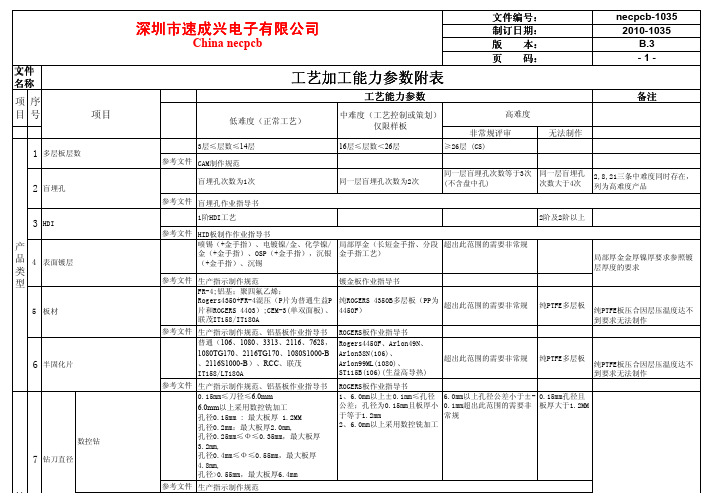
4MIL/20MIL 4MIL/20MIL 6MIL/30MIL 8MIL/30MIL <5/1:6 8MIL/20MIL 超出此范围的需要非常规
>6.0MM >6.0MM <0.15mm <0.40mm <0.80mm <1.00mm <1.20mm <1.50mm <1.80mm
3.0以上按4层板算
01mm超出此范围的需要非常规超出此范围的需要非常规参考文件厚径比1010厚径比12厚径比12参考文件30mm孔径65mm超出此范围的需要非常规参考文件90超出此范围的需要非常规参考文件01mm0075mm005mm005mm参考文件01mm或者客户无要求005孔径公差01mm005mm005mm参考文件0075mm005孔径公差0075mm005mm0025mm参考文件1210mil8孔与孔间距107孔与孔间距87mil34mil33mil33mil45mil354mil354mil354mil57mil56mil56mil55mil610mil69mil69mil68mil44mil34mil或者局部33mil33mil33mil局部33mil仅限gba区域芯片区域或者并排走线不超过5排46mil45mil45mil44mil58mil57mil57mil56mil812mil610mil610mil69mil79mil68mil68mil67mil911mil810mil810mil89mil1113mil1012mil1012mil1011mil1315mil1214mil1214mil1213mil过孔4mil3mil3mil器件孔8mil6mil6mil过孔5mil4mil3mil器件孔10mil8mil8mil过孔6mil5mil5mil器件孔12mil10mil10mil过孔8mil6mil6mil器件孔14mil12mil12mil线宽公差线宽公差2010线宽公差2010线宽间距必须满足1314要求孔径厚径比pthnpth孔位公差角度2821三条中难度同时存在列为高难度产品60mm以上金属化孔径公差参考序号7的要求孔径无法补偿情况下厚径比大于15激光钻孔外层最小线宽间距补偿前网格线宽间距最小焊环沉孔孔径公差内层最小线宽间距补偿前13141516891011钻孔图形转移铜厚35um铜厚75um铜厚105um铜厚18um铜厚35um铜厚75um铜厚105um铜厚35um铜厚75um铜厚105um铜厚18um铜厚35um铜厚75um铜厚105um铜厚18um生产指示制作规范生产指示制作规范孔到孔间距铜厚18umcam制作规范生产指示制作规范生产指示制作规范生产指示制作规范生产指示制作规范hid板制作作业指导书12mil10mil8mil6mil直径11mil80mil直径110mil直径8mil6mi
NEC电气标注说明书

❼❿❷❷❺❻❽❶❶❶❹❹❹❸❹❾†PER NEC 408.4(B) Part No. 558-00309†PER NEC 408.4(B)Roll: 558-00313†NOTE: Electrical Service equipment must be field marked per the NEC Code whenit is present in a building or structure (other thandwelling units) and supported by more than one serviceprovider (i.e., public utilities such as electricity and a PV System). This includes Arc Flash and informational labeling.†PER NEC 110.24(A) / Roll: 558-00313MAX AVAILABLE FAULT CURRENT: 46,552 AMPS DATE 2/15/12†NEC 230.2(E), NEC 230.72(A) / Roll: 558-00313SECOND SERVICE DISCONNECT ON NORTH SIDE OF BUILDINGINV1THIS PANEL FED FROM INV1†NEC Article 110.16 and NFPA 70E Article130.5(C)(1),(2),(3)Roll: 558-00381†NEC 210.5 (C)(1)(B)Roll: 558-00307A = BLACKB = REDC = BLUENEUTRAL = WHITEThe diagram shown in this poster is an illustration of one photovoltaic labeling scenario. The number and type of labels needed will vary based on the project scope and its related specifications. Check with AHJ for local requirements.UL1741allows the use of either PV or Photovoltaic on the pre-printed label.If no battery backupNEC 690.31(B)PHOTOVOLTAIC SYSTEMLABELINGREQUIREMENTSNEC 2017 Article 690 and IFC 2012FOR MARKING DC BACKUP SYSTEMS / Roll: 596-00240Combiner Box / Circuits / Conduit Combiner Box / Enclosures / EMT EnclosuresDC Disconnect / Breaker /Recombiner BoxEMT / Conduit Raceways*(Reflective Material Required)134AC Disconnect / Breaker / Points of ConnectionProduction / Net Meter (Bi-directional)76NEC 690.31(G)(3)(4) / Roll: 596-00206 / 10-Pk: 596-00678Building / Structure2NEC 705.10 & NEC 690.56(B)Roll: 558-00350POWER TO THIS SERVICE IS ALSO SUPPLIED FROM THE FOLLOWING SOURCES WITH DISCONNECTS LOCATED AS SHOWNCAUTIONNEC 690.13(B) / Roll: 596-0087810-Pk: 596-00893 / Metal 5-Pk: 596-00921WARNINGELECTRICAL SHOCK HAZARDTERMINALS ON THE LINE AND LOAD SIDES MAY BE ENERGIZEDIN THE OPEN POSITIONNEC 690.13(B) / Roll: 596-0087810-Pk: 596-00893 / Metal 5-Pk: 596-00921WARNINGELECTRICAL SHOCK HAZARDTERMINALS ON THE LINE AND LOAD SIDES MAY BE ENERGIZEDIN THE OPEN POSITIONNEC 690.13(B) / Roll: 596-0087810-Pk: 596-00893 / Metal 5-Pk: 596-00921WARNINGELECTRICAL SHOCK HAZARDTERMINALS ON THE LINE AND LOAD SIDES MAY BE ENERGIZEDIN THE OPEN POSITIONNEC 690.13(B) / Roll: 596-0087810-Pk: 596-00893 / Metal 5-Pk: 596-00921WARNINGELECTRICAL SHOCK HAZARDTERMINALS ON THE LINE AND LOAD SIDES MAY BE ENERGIZEDIN THE OPEN POSITIONNEC 110.27(C) & OSHA 1910.145(f)(7)Roll: 596-00499 / 10-Pk: 596-00664Metal 5-Pk: 596-00832NEC 690.13(B) / Roll: 596-0087910-Pk: 596-00894 / Metal 5-Pk: 596-00920WARNINGELECTRICAL SHOCK HAZARD TERMINALS ON THE LINE AND LOAD SIDES MAY BE ENERGIZEDIN THE OPEN POSITIONDC VOLTAGE IS ALWAYS PRESENTWHEN SOLAR MODULES ARE EXPOSED TO SUNLIGHTNEC 705.12(D)(3) & NEC 690.59 / Roll: 596-0049510-Pk: 596-09665 / Metal 5-Pk: 596-00833WARNING DUAL POWER SOURCESECOND SOURCE IS PHOTOVOLTAIC SYSTEMNEC 705.12(B)(3-4) & NEC 690.59 / Roll: 596-0049510-Pk: 596-09665 / Metal 5-Pk: 596-00833WARNING DUAL POWER SOURCESECOND SOURCE IS PHOTOVOLTAIC SYSTEMBreaker Panel / Pull Boxes8NEC 690.15 (C) & NEC 690.33(E)(2)Roll: 596-00244 / 10-Pk: 596-00671NEC 690.13 (F), NEC 705.12(D)(3-4) & NEC 690.59Roll: 596-00587 / 10-Pk: 596-00666Metal 5-Pk: 596-00834NEC 710.15(C) & 692.9 (C) / Roll: 596-0059110-Pk: 596-00699 / Metal 5-Pk: 596-00837Main Service Disconnect9NEC 690.13(B) / Roll: 596-0024310-Pk: 596-00675 / Metal 5-Pk: 596-00860NEC 690.13(B) / Roll: 596-0024310-Pk: 596-00675 / Metal 5-Pk: 596-00860Main Service Disconnect / Utility Meter10NEC 705.12 (B)(2)(c) / Roll: 596-0088310-Pk: 596-00884 / Metal 5-Pk: 596-00917NEC 690.31(G)(1) / Roll: 596-00257NEC 690.13(B) Each PV system disconnecting means shall plainly indicate whether in the open (off) or closed (on) position and be permanently marked “PV SYSTEM DISCONNECT” or equivalent. Additional markings shall be permitted based upon the specific system configuration. For PV system disconnecting means where the line and load terminals may be energized in the open position, the device shall be marked with the following words or equivalent.NEC 690.13(F) Type of Disconnect. A dc PV system disconnecting means shall be marked for use in PV systems or be suitable for backfeed operation.NEC 690.15(C) An isolating device shall be rated to open the maximum circuit current under load or be marked “Do Not Disconnect Under Load” or “Not for Current Interrupting.”NEC 690.31(B)(1) PV system circuit conductors shall be identified at all accessible points of termination, connection and splices. The means of identification shall be permitted by separate color coding, marking tape, tagging or other approved means. NEC 690.31(G)(1) Where circuits are embedded in build up, laminate or membrane roofing materials not covered by PV modules and associated equipment, the location of the circuits shall be clearly marked.Adhesive Fastened SignsANSI Z535.4-2011 Product Safety Signs and Labels, provides guidelines for suitable font sizes, words, colors, Symbols, andlocation requirements for labels. NEC 110.21(B)(1)The label shall be of sufficient durability to withstand theenvironment involved. NEC 110.21(B)(3)Adhesive fastened signs may be acceptable if properlyadhered. Vinyl signs shall be weather resistant. IFC 605.11.1.3Labels are not to scale.NEC 110.21(B)(1) FIELD APPLIED HAZARD MARKINGS: The marking shall shall meet the requirements in 110.21(B) and shall be readily visible and state Field Marking: Service equipment at other than dwelling units shall be legibly marked in the field with the maximum available fault current. The field marking(s) shall include the date the fault-current calculation was performed and be of sufficient durability to withstand the environment involved. The calculation shall be documented and made available to those authorized to A permanent plaque or directory, denoting the location of all electric power source disconnecting means on or in the premises, shall be installed at each service equipment location and at the location(s) of the system disconnect(s) for all electric power production sources capable of being interconnected. Also see 690.4(d) One sign required for each PV is required after 9/30/2011. Check latest 2012 NFPA Arc Flash requirements.OSHA 1910.145(f)(7)Warning tags are used to represent a hazard level between “Caution” and “Danger”.REQUIREMENTS FOR ELECTRICAL INSTALLATIONS (FIELD MARKING)LABELING REQUIREMENTS FOR ARTICLE 690NEC 690.31(G)(4) PV dc system circuit labels shall appear on every section of the wiring system that is separated by enclosures, walls, partitions, ceilings, or floors. Spacing between labels or markings, or between a label and a marking, shall not be more than 3 m (10 ft). Labels required in this section shall be suitable for the environment where they are installed.NEC 690.31(I) Solidly-grounded bipolar PV systems shall be clearly marked with a permanent, legible warning notice indicating that the disconnection of the grounded conductor(s) may result in overvoltage on the equipment.NEC 690.33(E)(2) Interruption of Circuit. Connectors shall be a type that requires the use of a tool to open and marked “Do Not Disconnect Under Load” or “Not for Current Interrupting.”NEC 690.52 Alternating-current modules shall be marked with identification of terminals or leads and with identification of the following ratings.NEC 690.53 A permanent label for the dc PV power source indicating items (1) through (3) shall be provided by the installer at dc PV system disconnecting means and at each dc equipment disconnecting means required by 690.15. Where a disconnecting means has more than one dc PV power source, the values in 690.53 (1) through (3) shall be specified for each source.NEC 690.54 All interactive system(s) points of interconnection with other sources shall be marked as an accessible location at the disconnecting means as a power source and with the rated ac output current and the nominal operating ac voltage.NEC 690.55 The PV system output circuit conductors shall be marked to indicate polarity where connected to energy storage systems.NEC 690.56(B) Plaques or directories shall be installed in accordance with 705.10.NEC 690.56(C)(3) A rapid shutdown switch shall have a label located on or no more than 1 meter (3 ft) from the switch that includes the following wording.NEC 690.56(C)(1)(a-b) The type of PV system shall be labeled as described in a) or b):NEC 690.59 PV systems connected to other sources shall be installed in accordance with Parts I and II of Article 705.NEC 690.13(B)Roll: 596-00238 / 10-Pk: 596-00854Hand-writable 5-Pk:596-00842Engravable 5-Pk:596-00858NEC 690.13(B) / Roll: 596-00237 / 10-Pk: 596-00853Hand-writable 5-Pk:596-00841Engravable 5-Pk:596-00857NEC 690.54 / Roll: 596-00892 / 10-Pk: 596-00882PHOTOVOLTAIC AC DISCONNECTRATED AC OUTPUT CURRENT:NOMINAL OPERATING AC VOLTAGEPHOTOVOLTAIC AC DISCONNECTRATED AC OUTPUT CURRENT:NOMINAL OPERATING AC VOLTAGEHand-writable 5-Pk:596-00919Engravable 5-Pk:596-00923NEC 690.54 / Roll: 596-00892 / 10-Pk: 596-00882PHOTOVOLTAIC AC DISCONNECTRATED AC OUTPUT CURRENT:NOMINAL OPERATING AC VOLTAGEHand-writable 5-Pk:596-00919Engravable 5-Pk:596-00923Hand-writable 5-Pk:596-00918Engravable 5-Pk:596-00922NEC 690.53 / Roll: 596-00891 / 10-Pk: 596-00881MAXIMUM VOLTAGEMAXIMUM CIRCUIT CURRENT MAX RATED OUTPUT CURRENT OF THE CHARGE CONTROLLER OR DC-TO-DC CONVERTER (IF INSTALLED)MAXIMUM VOLTAGEMAXIMUM CIRCUIT CURRENT MAX RATED OUTPUT CURRENT OF THE CHARGE CONTROLLER OR DC-TO-DC CONVERTER (IF INSTALLED)MAXIMUM VOLTAGEMAXIMUM CIRCUIT CURRENT MAX RATED OUTPUT CURRENT OF THE CHARGE CONTROLLER OR DC-TO-DC CONVERTER (IF INSTALLED)Inverter5NEC 690.54 / Roll: 596-00892 / 10-Pk: 596-00882Hand-writable 5-Pk:596-00919Engravable 5-Pk:596-00923NEC 690.31(I) / Roll: 596-0932310-Pk: 596-09324 / Metal 5-Pk: 596-00924WARNINGTHE DISCONNECTION OF THE GROUNDED CONDUCTOR(S)MAY RESULT IN OVERVOLTAGEON THE EQUIPMENTNEC 690.52 / Roll: 596-00252 / 10-Pk: 596-00855Hand-writable 5-Pk:596-00840Engravable 5-Pk:596-00862NEC 110.27(C) & OSHA 1910.145(f)(7)Roll: 596-00499 / 10-Pk: 596-00664Metal 5-Pk: 596-00832NEC 110.27(C) & OSHA 1910.145(f)(7)Roll: 596-00499 / 10-Pk: 596-00664Metal 5-Pk: 596-00832SOLAR ELECTRIC PV PANELSNEC 690.56(C)(3)Roll: 596-00887IFC 605.11.3.1(1) & 690.56(C)(1)(a)Roll: 596-00885IFC 605.11.3.1(2) & 690.56(C)(1)(b)Roll: 596-00886WARNINGPOWER SOURCE OUTPUT CONNECTION. DO NOT RELOCATE THIS OVERCURRENT DEVICE.。
AT32 USB接口ESD保护设计指南说明书

AN0034Application Note ESD protection design guide for AT32 USB interfaceIntroductionThis application note provides ESD protection design guide for AT32 USB 2.0 interface.ContentsOverview (5)ESD protection design guide (7)Selection of ESD protection device (8)Clamping voltage (8)Signal integrity (8)Revision history (9)Table 1. JS-001-2017 standard classification (5)Table 2. IEC61000-4-2 standard classification (6)Table 3. Document revision history (9)Figure 1. JS-001-2017 standard test waveform (5)Figure 2. IEC61000-4-2 standard test waveform (6)Figure 3. USB ESD protection circuit (7)Figure 4. VBUS detection circuit (7)OverviewThe hot-pluggable characteristics of the USB interface is susceptible to electrostatic discharge that damages the components, such as, crash, board burning, and disconnection and so on. It is necessary to design ESD protection on the USB interface following the two standards of JS-001-2017 (HBM) and IEC61000-4-2. HBM requires that the USB interface is capable of withstanding up to 2 kV discharge. Figure 1 and Table 1 shows JS-001-2017 standard test waveform and classification, and Figure 2 and Table 2 shows IEC61000-4-2 standard test waveform and classification.Figure 1. JS-001-2017 standard test waveformTable 1. JS-001-2017 standard class levelFigure 2. IEC61000-4-2 standard test waveformTable 2. IEC61000-4-2 standard class levelESD protection design tipsIt is recommended to add ESD protection device and VBUS monitoring circuit to detect overvoltage when designing USB interface. Design tips are as follows:● ESD protection device should be placed close to the USB socket interface (ESD entry point) asmuch as possible● VBUS, USB data line (USB_D+/USB_D-) and ID (if OTG) must be protected against ESD.Figure 3. USB ESD protection circuit ● VBUS track should be isolated from D+/D- as much as possible●The metal housing of USB socket must be connected to the device housing ground ● When the VBUS supply is not neededed, it can be connected to non-5V-tolerant I/O through aresistor voltage divider, or to 5V-tolerant GPIO directly, used as VBUS detection signal.Figure 4. VBUS detection circuitSelection of ESD protection deviceThe transmission rate of USB2.0 FS reaches up to 12 Mbps, and thus TVS array diodes are generally used for ESD protection. When an ESD event arrives, the diode in TVS can be forward-conducted so that the transient current bypasses the sensitive CMOS component and the transient high voltage is reduced to the clamp voltage value in order to protect the interface circuit against ESD damage.Clamping voltageWhen ESD events are generated, the protection device limits the high voltage pulse to the clamping voltage, and shunts most of the pulse current to the ground in order to protect the back-end sensitive devices. However, there are still some residual current flowing into the protected device. The peak current during ESD event period is the sum of the shunt current passing through ESD protection device and the residual current flowing into the protected device. The power imposed on the protected device depends on the clamping voltage and the residual current. Clamping voltage can be calculated based on the formula:Clamping voltage (VCL) = VBR + Io (residual current) x Ro (resistance of the protected device)For the selection of the clamping voltage of the ESD protection device, the designer must understand which kind of test conditions to be used for determining the value. Based on IEC61000-4-2 Level 4 standard, ESD pulse has the rise time less than 1ns and the duration less than 100 ns, as well as 30A peak current.ESD protection diode with a clamping voltage of 5V may exceed 30V during the actual ESD test. Without this understanding, the designer may select ESD protection devices according to the minimum clamping voltage in the datasheet.Signal integrityThe data transmission system requires that the receptors achieve a certain level of signal integrity. The rise time and fall time of the signal is limited by the impedance of the overall transmission path, along with all parasitic capacitances of the interface. These parasitic capacitances may be introduced by mismatched PCB tracks, USB socket pins or other paralleling capacitances. Therefore it is required that the capacitances of ESD protection devices must be smaller and have the capability to provide ESD protection.Revision historyDate Revision Changes 2019.08.20 1.0.0 Initial release2022.3.1 2.0.0 1. Added AT32F435/437/425 to the applicable product list2. Updated the description of 2 ESD protection design tipsIMPORTANT NOTICE – PLEASE READ CAREFULLYPurchasers are solely responsible for the selection and use of ARTERY’s products and services, and ARTERY assumes no liability whatsoever relating to the choice, selection or use of the ARTERY products and services described herein.No license, express or implied, to any intellectual property rights is granted under this document. If any part of this document deals with any third party products or services, it shall not be deemed a license grant by ARTERY for the use of such third party products or services, or any intellectual property contained therein, or considered as a warranty regarding the use in any manner whatsoever of such third party products or services or any intellectual property contained therein.Unless otherwise specified in ARTERY’s terms and conditions of sale, ARTERY provides no warranties, express or implied, regarding the use and/or sale of ARTERY products, including but not limited to any implied warranties of merchantability, fitness for a particular purpose (and their equivalents under the laws of any jurisdiction), or infringement of any patent, copyright or other intellectual property right.Purchasers hereby agrees that ARTERY’s products are not designed or authorized for use in: (A) any application with special requirements of safety such as life support and active implantable device, or system with functional safety requirements; (B) any air craft application; (C) any automotive application or environment; (D) any space application or environment, and/or (E) any weapon application. Purchasers’ unauthorized use of them in the aforementioned applications, even if with a written notice, is solely at purchasers’ risk, and is solely responsible for meeting all legal and regulatory requirement in such use.Resale of ARTERY products with provisions different from the statements and/or technical features stated in this document shall immediately void any warranty grant by ARTERY for ARTERY products or services described herein and shall not create or expand in any manner whatsoever, any liability of ARTERY.© 2022 Artery Technology -All rights reserved。
NEC EXPRESSCLUSTER X 5.1 产品说明书
Version 5.1 New EnhancementNovember 2023NECTechnology Service and Software Department (EXPRESSCLUSTER)EXPRESSCLUSTER RoadmapProviding various platforms with high availability in accordance with the timesEnhancement Points of EXPRESSCLUSTER X 5.1Enhancements for the cloud ⚫Added forced-stop resources for Azure.⚫Mail Report function supports SMTPS and STARTTLS.⚫Facilitated the configuration and operation processes in the cloud environment.Security enhancements⚫Added the function to display operation logs of the Cluster WebUI.⚫Added the function to configure the log storage period.⚫Added the function to configure a floating IP resource as a source IP address.⚫Supported OpenSSL 3.0.Newly supported platforms & applications ⚫SUSE Linux Enterprise Server 15 SP4⚫Ubuntu Server22.04.1 LTS, Ubuntu Server20.04.5 LTS⚫SQL Server2022,PostgreSQL 15.1, MariaDB 8.0.31,MariaDB 10.10⚫ReFSEnhancements for the CloudAdded forced-stop resources for Azure.Mail Report function supports SMTPS and STARTTLS.Facilitated the configuration and operation processes in the cloud environment.Added Forced-stop Resources for AzureThe forced-stop function that prevents both-system activation due to a hang-up has been enhanced: GUI configuration now allows using the function to forcedly stop a failed node before failover.This can be configured from GUI withoutscripting.Availability SetResource GroupVMBlob storageFault Domain 0Fault Domain 1MirroringVMBlob storageForcedly stop a failed node before theoperation startup![Cluster WebUI] ->[Cluster Properties]-> [Fencing]tab-> [Forced Stop] FailureOperationOperation◆Mail Report function is now available for SMTPS/STARTTLS-required email delivery services such as “Email Delivery”, email delivery service on OCI.Mail Report function is now supported on Oracle Cloud Infrastructure (OCI).Oracle Cloud InfrastructureAvailability DomainEmail DeliverySSL(TLS)Internet!System AdministratorFailure*This enhanced function is available in the on-premises environment as well.Mail Report function supports SMTPS and STARTTLSOther Facilitation Improvements in Configuration and Operation on the Cloud Environment◆For configuration◼Environment variables for using AWS-related functions (such as AWS virtual IP resources) now can be configured from the Cluster WebUI. This allows the configuration without going through a proxy to be set on the Cluster WebUI, for example, only when EXPRESSCLUSTER uses AWS-related functions.◼Added the function for specifying a command line option, to the AWS CLI being executed with the AWS-related function. This allows specifying the end point for executing the AWS CLI.◼Installing Python is not needed anymore in the configuration using only the AWS virtual IPresource and the AWS virtual IP monitor resource.◼Installing the VMware vSphere CLI is not needed anymore to use the forced-stop function in the vSphere environment.◆For operation*This enhanced function is available in the on-premises environment as well.◼Added the option not to execute the OS restart, to the backup/restore commands(clpbackup/clprestore). This now allows some procedures to be performed without the OS restart.Security EnhancementsAdded the function to display operation logs of the Cluster WebUI.Added the function to configure the log storage period.Added the function to configure a floating IP resource as a source IP address. Supported OpenSSL 3.0.Added the Function to Display Operation Logs of the Cluster WebUIAdded the tab to display the history of operations performed on the Cluster WebUI: It is now possible to check traces of incorrect or invalid operations.At [2:07:20 am, May 17, 2023], by the user [clpuser2], from the IP address [10.20.10.200], the group [failover] was requested to move to the server [server22].At [2:08:28 am, May 17, 2023], by the user [clpuser1], from the IP address [10.20.10.200], the properties of the group [failover] were viewed.When, by whom, from where, what operation was performed now can be checked on the Cluster WebUI!Added the Function to Configure the Log Storage PeriodItems to configure for the log storage period have been added to the Cluster WebUI: It is now easy to address the requirements for the log storage.Examples of guidelines for the log storage period◆PCI Data Security Standard v4.0 (*1)◼10.5.1 Retain audit log history for at least 12 months , with at least the most recent three months immediately available for analysis.◆Convention on Cybercrime (ETS No. 185) (*2)◼oblige that person to preserve and maintain the integrity of that computer data for a period as long as necessary, up to a maximum of ninety days◆NIST SP 800-92 (Guide to Computer Security Log Management) (*3)◼Table 4-1. Examples of Logging Configuration SettingsLogs can be compressed, stored to the logstorage directory at the specified time such as the one with low server load, and kept for the desired storage period.(*1) https:///document_library/(*2) https://www.coe.int/en/web/conventions/full-list?module=treaty-detail&treatynum=185(*3)https:///nistpubs/legacy/sp/nistspecialpublication800-92.pdf[Cluster WebUI] ->[Cluster Properties]-> [Extension] tab-> [Settings of log storage period]Added the Function to Configure a Floating IP Address as a Source IP Address Items to configure a floating IP address as a source IP address have been added to the Cluster WebUI: The number of ports to be opened in the firewall now can be minimized as needed.◆Before◆The source IP is not fixed. (Actual IP or floating IP)◼If the firewall restricts the source IP address, all the IP addressesneed to be opened.◼If a failover occurs, the source IP address changes, and then theserver communicating with the cluster server behaves in anunexpected way.◆After ◆The source IP is fixed to the floating IP.◼If the firewall restricts the source IP address, only the floating IP address needs to be opened.◼Even if a failover occurs, the source IP address remains unchanged. This allows the server communicating with the cluster server to behave without being aware of the failover.Actual IPs of servers Source IP:10.0.0.10 ?10.0.0.20 ?10.0.0.30 ?Source IP:10.0.0.1010.0.0.2010.0.0.3010.0.0.1010.0.0.2010.0.0.3010.0.0.10Floating IP [Cluster WebUI] -> Properties of Floating IP resource -> [Detail] tab *This function is available also for applications where the clients are aware of the source IPs.Other Security Enhancements◆Supported OpenSSL 3.0◼HTTPS access to the Cluster WebUI◼HTTPS monitoring function by HTTP monitor resource◼FTPS monitoring function by FTP monitor resource◼Mail report function (Communication with the mail server by using SMTPS/STARTTLS)◆Disabled TLS 1.1◼HTTPS access to the Cluster WebUINewly Supported Platforms and ApplicationsNewly Supported Platforms and Applications◆OS◼RedHatEnterprise Linux9.2,9.0,8.8◼MIRACLE LINUX9.2,9.0,8.8◼Oracle Linux9.2,9.0,8.8◼SUSE Linux Enterprise Server 15 SP5/SP4◼Ubuntu Server22.04.1 LTS◼Ubuntu Server20.04.5 LTS◼AlmaLinux OS9.2,9.0,8.8◆Data base◼SQL Server 2022◼PostgreSQL 15.1◼MariaDB 8.0.31◼MariaDB 10.10◆File system◼ReFS◆Java execution environment◼Java17◆Java application◼WebSAM SVF PDF Enterprise 10.1◼WebSAM RDE SUITE 10.1◼WebSAM SVF Connect SUITE Standard 10.1Thank YouAn Integrated High Availability and Disaster Recovery Solution For more product information & request for trial license, visit >>https:///expresscluster/For more information, feel free to contact us -https:///en/global/prod/expresscluster/en/contact.html。
NEC V984Q C981Q 安装指南说明书

V984Q/C981Q
Page 1 of 12
Ventilation Recommendations:
Dimensions below are minimum required for proper ventilation.
NEC Display Solutions of America, Inc.
Tilt Angle and Rotation:
• Below is the maximum angle the monitor can be tilted. Note that the monitor can only be tilted in the landscape position.
Weight with stand:
BTU’s:
1791.37 BTU/hour (C981Q), 2217.89 BTU/hour (V984Q)
86.4” (W) x 49.2” (L) x 3.7” (D) 86.4”(W) x 50.6”(H) x 23.9”(D) 204.8 lbs. / 92.9kg 214.5 lbs. / 97.3kg
NEC Display Solutions of America, Inc.
V984Q/C981Q
Page 8 of 12
NEC Display Solutions of America, Inc.
Compute Module Integration:
• Door on the back of the display can be opened by loosening captive screws. • Separate IO Board is necessary to accompany RPi Compute Module in unit
NEC 2U 设备扩展单元配置指南说明书
2U Device Expansion Unit Configuration GuideIntroductionThis document contains product and configuration information that will enable you to configure your system. The guide will ensure fast and proper configuration of your storage system.September 17, 2014Revision 2.0NEC CorporationContentsTECHNICAL SPECIFICATION (3)Key Features (3)Specification (3)EXTERNAL VIEWS (4)Front and Rear Views (4)Dimensions (mm) (5)UNIT CONFIGURATION (6)1External Tape Drive Enclosure (6)1.1Tape Drive Configuration (6)1.2SAS Tape Drive Configuration (8)1.3USB Tape/RDX Drive Configuration (10)1.4SAS and USB Tape/RDX Drive Configuration (12)COPYRIGHT NOTICE AND LIABILITY DISCLAIMER (18)REVISION HISTORY (19)Technical SpecificationKey Features●Affordable direct attached data protection solution for rack mount systems●Four 5-inch half height drive bays in 2U enclosure●Flexible configuration with SAS and USB tape drive installation●Superior reliability with redundant power suppliesSpecificationN8141-59F5-inch Media Bays 4Number of Interface Kits Four 6Gbps SAS and/or USB 2.0 interface cablesTwo internal 6Gbps SAS cables included Redundant Power Supply Optional, non-hot plugPower Supply 100-240 VAC ± 10% 50 / 60 Hz ± 3 HzMaximum Power Consumption 450 VADimensions (W x D x H ) 424.0 x 660.2 x 87.3 mm / 18.8 x 21.2 x 3.4 in (2U)Maximum Weight 9.8 kg, 21.60 lbs.Temperature, Relative Humidity (non-condensing) Operating: 10° to 35° C / 50° to 95° F, 10 to 80%Non-Operating: -10° to 55° C / 14° to 131° F, 10 to 80%External ViewsFront and Rear ViewsFront ViewSystem Status 1 LED Drive Bays B.System Status 2 LEDRear ViewAC Inlet External Connector 1 B. Power Switch F. External Connector 2 C. AC Inlet (Optional) G. External Connector 3 D.Power Switch (Optional)H.External Connector 4A BABEF G HCDDimensions (mm)Unit Configuration1 External Tape Drive Enclosure1.1Tape Drive ConfigurationRefer to the section in accordance with type of tape drives installed and number of host adapters.Refer to 1.4.4 SAS Tape DrivesMixing SAS and USB Tape DrivesRefer to 1.2.1 Refer to 1.2.2 One SAS HBA One USB and One SAS HBA Refer to 1.4.1 One USB and Two SAS HBARefer to 1.4.2 Refer to 1.4.3 One USB and Three SAS HBATwo USB and One SAS HBAThree SAS HBARefer to 1.2.3 Two SAS HBA Four SAS HBARefer to 1.2.4 Refer to 1.3.1 USB Tape DrivesOne USB HBA Refer to 1.3.2Two USB HBARefer to 1.3.3 Three USB HBA Refer to 1.3.4Four USB HBATwo USB and Two SAS HBARefer to 1.4.5 Three USB and One SAS HBARefer to 1.4.6Dividing Tape Drive BaysThe tape drive enclosure can be shared with up to four servers, HBAs. See below the figures for typical tape drive bays configuration.Two HBA Configuration - SAS InterfacesThree HBA Configuration – Mixing SAS and USB InterfacesFour HBA Configuration – Mixing SAS and USB InterfacesTo HBATo HBASAS InterfaceSAS InterfaceTo HBATo HBA To HBASAS or USB Interface SAS or USB InterfaceSAS InterfaceTo HBA To HBATo HBA To HBASAS or USB InterfaceSAS or USB Interface SAS or USB Interface SAS or USB Interface1.2 SAS Tape Drive Configuration1.2.1 One SAS HBARequired LSI SAS9212-4i4e Host Bus Adapter6Gb/s SAS, Int. 4 / Ext. 4, 7-pin SATA / SFF-8088, PCIe 2.0 x8N8103-142Cable Required External SAS Cable2 m, 1 x SFF-8088 to 1 x SFF-8088K410-191(02)Enclosure Required 2U Device Expansion Unit4 x 5-inch media baysN8141-59FCable Internal SAS Cable1 x SFF-8088 to2 x SFF-8482, mount bracket included, 2 pcs.StandardPower supply Recommended Power unitNon-hot plug power supplyN8181-54FDrive2 slots available Internal LTO (SAS)LTO3, Half height, Native capacity 400 GBN8151-102Internal LTO (SAS)LTO4, Half height, Native capacity 800 GBN8151-90 Internal LTO (SAS)LTO5, Half height, Native capacity 1.5 TBN8151-103 Internal LTO (SAS)LTO6, Half height, Native capacity 2.5 TBN8151-1061.2.2 Two SAS HBA2 Required LSI SAS9212-4i4e Host Bus Adapter6Gb/s SAS, Int. 4 / Ext. 4, 7-pin SATA / SFF-8088, PCIe 2.0 x8N8103-142Cable2 Required External SAS Cable2 m, 1 x SFF-8088 to 1 x SFF-8088K410-191(02)Enclosure Required 2U Device Expansion Unit4 x 5-inch media baysN8141-59FCable Internal SAS Cable1 x SFF-8088 to2 x SFF-8482, mount bracket included, 2 pcs.StandardPower supply Recommended Power unitNon-hot plug power supplyN8181-54FDrive2 slots per HBA available Internal LTO (SAS)LTO3, Half height, Native capacity 400 GBN8151-102Internal LTO (SAS)LTO4, Half height, Native capacity 800 GBN8151-90 Internal LTO (SAS)LTO5, Half height, Native capacity 1.5 TBN8151-103 Internal LTO (SAS)LTO6, Half height, Native capacity 2.5 TBN8151-1061.2.3 Three SAS HBA3 Required LSI SAS9212-4i4e Host Bus Adapter6Gb/s SAS, Int. 4 / Ext. 4, 7-pin SATA / SFF-8088, PCIe 2.0 x8Cable3 Required External SAS Cable2 m, 1 x SFF-8088 to 1 x SFF-8088K410-191(02)Enclosure Required 2U Device Expansion Unit4 x 5-inch media baysN8141-59FCable Internal SAS Cable1 x SFF-8088 to2 x SFF-8482, mount bracket included, 2 pcs.StandardCable Required Internal SAS Cable1 x SFF-8088 to2 x SFF-8482, mount bracket includedK410-249(00)Power supply Recommended Power unitNon-hot plug power supplyN8181-54FDriveOne 2 slots per HBA and two 1 slots per HBA available Internal LTO (SAS)LTO3, Half height, Native capacity 400 GBN8151-102Internal LTO (SAS)LTO4, Half height, Native capacity 800 GBN8151-90 Internal LTO (SAS)LTO5, Half height, Native capacity 1.5 TBN8151-103 Internal LTO (SAS)LTO6, Half height, Native capacity 2.5 TBN8151-1061.2.4 Four SAS HBA4 Required LSI SAS9212-4i4e Host Bus Adapter6Gb/s SAS, Int. 4 / Ext. 4, 7-pin SATA / SFF-8088, PCIe 2.0 x8N8103-142Cable4 Required External SAS Cable2 m, 1 x SFF-8088 to 1 x SFF-8088K410-191(02)Enclosure Required 2U Device Expansion Unit4 x 5-inch media baysN8141-59FCable Internal SAS Cable1 x SFF-8088 to2 x SFF-8482, mount bracket included, 2 pcs.StandardCable2 Required Internal SAS Cable1 x SFF-8088 to2 x SFF-8482, mount bracket includedK410-249(00)Power supply Recommended Power unitNon-hot plug power supplyN8181-54FDrive1 slots per HBA available Internal LTO (SAS)LTO3, Half height, Native capacity 400 GBN8151-102Internal LTO (SAS)LTO4, Half height, Native capacity 800 GBN8151-90 Internal LTO (SAS)LTO5, Half height, Native capacity 1.5 TBN8151-103 Internal LTO (SAS)LTO6, Half height, Native capacity 2.5 TBN8151-1061.3 USB Tape/RDX Drive Configuration 1.3.1 One USB HBA1 x USB portCable Required External USB Cable2 m, 1 x external USB to 1 x USB device, mount bracketincludedK410-197(00)Enclosure Required 2U Device Expansion Unit4 x 5-inch media baysN8141-59FPower supply Recommended Power unitNon-hot plug power supplyN8181-54FDrive1 slots available Internal DAT (USB)DDS3 / DDS4 / DAT72, Native capacity 36 GBNOTE: DDS1 / DDS2 format are not supported.N8151-69AInternal DAT (USB)DDS4 / DAT72 / DAT160, Native capacity 80 GBNOTE: DDS1 / DDS2 / DDS3 format are not supported.N8151-78A Internal RDX (USB) N8151-1051.3.2 Two USB HBA2 x USB portCable2 Required External USB Cable2 m, 1 x external USB to 1 x USB device, mount bracketincludedK410-197(00)Enclosure Required 2U Device Expansion Unit4 x 5-inch media baysN8141-59FPower supply Recommended Power unitNon-hot plug power supplyN8181-54FDrive1 slots per HBA available Internal DAT (USB)DDS3 / DDS4 / DAT72, Native capacity 36 GBNOTE: DDS1 / DDS2 format are not supported.N8151-69AInternal DAT (USB)DDS4 / DAT72 / DAT160, Native capacity 80 GBNOTE: DDS1 / DDS2 / DDS3 format are not supported.N8151-78A Internal RDX (USB) N8151-1051.3.3 Three USB HBA3 x USB portCable3 Required External USB Cable2 m, 1 x external USB to 1 x USB device, mount bracketincludedK410-197(00)Enclosure Required 2U Device Expansion Unit4 x 5-inch media baysN8141-59FPower supply Recommended Power unitNon-hot plug power supplyN8181-54FDrive1 slots per HBA available Internal DAT (USB)DDS3 / DDS4 / DAT72, Native capacity 36 GBNOTE: DDS1 / DDS2 format are not supported.N8151-69AInternal DAT (USB)DDS4 / DAT72 / DAT160, Native capacity 80 GBNOTE: DDS1 / DDS2 / DDS3 format are not supported.N8151-78A Internal RDX (USB) N8151-1051.3.4 Four USB HBA4 x USB portCable4 Required External USB Cable2 m, 1 x external USB to 1 x USB device, mount bracketincludedK410-197(00)Enclosure Required 2U Device Expansion Unit4 x 5-inch media baysN8141-59FPower supply Recommended Power unitNon-hot plug power supplyN8181-54FDrive1 slots per HBA available Internal DAT (USB)DDS3 / DDS4 / DAT72, Native capacity 36 GBNOTE: DDS1 / DDS2 format are not supported.N8151-69AInternal DAT (USB)DDS4 / DAT72 / DAT160, Native capacity 80 GBNOTE: DDS1 / DDS2 / DDS3 format are not supported.N8151-78A Internal RDX (USB) N8151-1051.4 SAS and USB Tape/RDX Drive Configuration 1.4.1 One USB HBA and One SAS HBA1 x USB portStorage Controller Required SAS ControllerLSI SAS9212-4i4e Host Bus Adapter6Gb/s SAS, Int. 4 / Ext. 4, 7-pin SATA / SFF-8088, PCIe 2.0 x8N8103-142Cable Required External USB Cable2 m, 1 x external USB to 1 x USB device, mount bracketincludedK410-197(00)Cable Required External SAS Cable2 m, 1 x SFF-8088 to 1 x SFF-8088K410-191(02)Enclosure Required 2U Device Expansion Unit4 x 5-inch media baysN8141-59FPower supply Recommended Power unitNon-hot plug power supplyN8181-54FCable Internal SAS Cable1 x SFF-8088 to2 x SFF-8482, mount bracket included, 2 pcs.StandardDrive1 slot per USB HBA and2 slots per SAS HBA available USB Internal DAT (USB)DDS3 / DDS4 / DAT72, Native capacity 36 GBNOTE: DDS1 / DDS2 format are not supported.N8151-69AInternal DAT (USB)DDS4 / DAT72 / DAT160, Native capacity 80 GBNOTE: DDS1 / DDS2 / DDS3 format are not supported.N8151-78A Internal RDX (USB) N8151-105SAS Internal LTO (SAS)LTO3, Half height, Native capacity 400 GBN8151-102 Internal LTO (SAS)LTO4, Half height, Native capacity 800 GBN8151-90 Internal LTO (SAS)LTO5, Half height, Native capacity 1.5 TBN8151-103 Internal LTO (SAS)LTO6, Half height, Native capacity 2.5 TBN8151-1061 x USB portStorage Controller 2 Required SAS ControllerLSI SAS9212-4i4e Host Bus Adapter6Gb/s SAS, Int. 4 / Ext. 4, 7-pin SATA / SFF-8088, PCIe 2.0 x8N8103-142Cable Required External USB Cable2 m, 1 x external USB to 1 x USB device, mount bracketincludedK410-197(00)Cable2 Required External SAS Cable2 m, 1 x SFF-8088 to 1 x SFF-8088K410-191(02)Enclosure Required 2U Device Expansion Unit4 x 5-inch media baysN8141-59FPower supply Recommended Power unitNon-hot plug power supplyN8181-54FCable Internal SAS Cable1 x SFF-8088 to2 x SFF-8482, mount bracket included, 2 pcs.StandardDrive1 slot per USB HBA and 1 to2 slots per SAS HBA available USB Internal DAT (USB)DDS3 / DDS4 / DAT72, Native capacity 36 GBNOTE: DDS1 / DDS2 format are not supported.N8151-69AInternal DAT (USB)DDS4 / DAT72 / DAT160, Native capacity 80 GBNOTE: DDS1 / DDS2 / DDS3 format are not supported.N8151-78A Internal RDX (USB) N8151-105SAS Internal LTO (SAS)LTO3, Half height, Native capacity 400 GBN8151-102 Internal LTO (SAS)LTO4, Half height, Native capacity 800 GBN8151-90 Internal LTO (SAS)LTO5, Half height, Native capacity 1.5 TBN8151-103 Internal LTO (SAS)LTO6, Half height, Native capacity 2.5 TBN8151-1061 x USB portStorage Controller 3 Required SAS ControllerLSI SAS9212-4i4e Host Bus Adapter6Gb/s SAS, Int. 4 / Ext. 4, 7-pin SATA / SFF-8088, PCIe 2.0 x8N8103-142Cable Required External USB Cable2 m, 1 x external USB to 1 x USB device, mount bracketincludedK410-197(00)Cable3 Required External SAS Cable2 m, 1 x SFF-8088 to 1 x SFF-8088K410-191(02)Enclosure Required 2U Device Expansion Unit4 x 5-inch media baysN8141-59FPower supply Recommended Power unitNon-hot plug power supplyN8181-54FCable Internal SAS Cable1 x SFF-8088 to2 x SFF-8482, mount bracket included, 2 pcs.StandardCable Required Internal SAS Cable1 x SFF-8088 to2 x SFF-8482, mount bracket includedK410-249(00)Drive1 slot per HBA available USB Internal DAT (USB)DDS3 / DDS4 / DAT72, Native capacity 36 GBNOTE: DDS1 / DDS2 format are not supported.N8151-69AInternal DAT (USB)DDS4 / DAT72 / DAT160, Native capacity 80 GBNOTE: DDS1 / DDS2 / DDS3 format are not supported.N8151-78A Internal RDX (USB) N8151-105SAS Internal LTO (SAS)LTO3, Half height, Native capacity 400 GBN8151-102 Internal LTO (SAS)LTO4, Half height, Native capacity 800 GBN8151-90 Internal LTO (SAS)LTO5, Half height, Native capacity 1.5 TBN8151-103 Internal LTO (SAS)LTO6, Half height, Native capacity 2.5 TBN8151-1062 x USB portStorage Controller 1 Required SAS ControllerLSI SAS9212-4i4e Host Bus Adapter6Gb/s SAS, Int. 4 / Ext. 4, 7-pin SATA / SFF-8088, PCIe 2.0 x8N8103-142Cable2 Required External USB Cable2 m, 1 x external USB to 1 x USB device, mount bracketincludedK410-197(00)Cable Required External SAS Cable2 m, 1 x SFF-8088 to 1 x SFF-8088K410-191(02)Enclosure Required 2U Device Expansion Unit4 x 5-inch media baysN8141-59FPower supply Recommended Power unitNon-hot plug power supplyN8181-54FCable Internal SAS Cable1 x SFF-8088 to2 x SFF-8482, mount bracket included, 2 pcs.StandardDrive1 slot per USB HBA and2 slots per SAS HBA available USB Internal DAT (USB)DDS3 / DDS4 / DAT72, Native capacity 36 GBNOTE: DDS1 / DDS2 format are not supported.N8151-69AInternal DAT (USB)DDS4 / DAT72 / DAT160, Native capacity 80 GBNOTE: DDS1 / DDS2 / DDS3 format are not supported.N8151-78A Internal RDX (USB) N8151-105SAS Internal LTO (SAS)LTO3, Half height, Native capacity 400 GBN8151-102 Internal LTO (SAS)LTO4, Half height, Native capacity 800 GBN8151-90 Internal LTO (SAS)LTO5, Half height, Native capacity 1.5 TBN8151-103 Internal LTO (SAS)LTO6, Half height, Native capacity 2.5 TBN8151-1062 x USB portStorage Controller 2 Required SAS ControllerLSI SAS9212-4i4e Host Bus Adapter6Gb/s SAS, Int. 4 / Ext. 4, 7-pin SATA / SFF-8088, PCIe 2.0 x8N8103-142Cable2 Required External USB Cable2 m, 1 x external USB to 1 x USB device, mount bracketincludedK410-197(00)Cable2 Required External SAS Cable2 m, 1 x SFF-8088 to 1 x SFF-8088K410-191(02)Enclosure Required 2U Device Expansion Unit4 x 5-inch media baysN8141-59FPower supply Recommended Power unitNon-hot plug power supplyN8181-54FCable Internal SAS Cable1 x SFF-8088 to2 x SFF-8482, mount bracket included, 2 pcs.StandardDrive1 slot per HBA available USB Internal DAT (USB)DDS3 / DDS4 / DAT72, Native capacity 36 GBNOTE: DDS1 / DDS2 format are not supported.N8151-69AInternal DAT (USB)DDS4 / DAT72 / DAT160, Native capacity 80 GBNOTE: DDS1 / DDS2 / DDS3 format are not supported.N8151-78A Internal RDX (USB) N8151-105SAS Internal LTO (SAS)LTO3, Half height, Native capacity 400 GBN8151-102 Internal LTO (SAS)LTO4, Half height, Native capacity 800 GBN8151-90 Internal LTO (SAS)LTO5, Half height, Native capacity 1.5 TBN8151-103 Internal LTO (SAS)LTO6, Half height, Native capacity 2.5 TBN8151-1063 x USB portStorage Controller Required SAS ControllerLSI SAS9212-4i4e Host Bus Adapter6Gb/s SAS, Int. 4 / Ext. 4, 7-pin SATA / SFF-8088, PCIe 2.0 x8N8103-142Cable3 Required External USB Cable2 m, 1 x external USB to 1 x USB device, mount bracketincludedK410-197(00)Cable Required External SAS Cable2 m, 1 x SFF-8088 to 1 x SFF-8088K410-191(02)Enclosure Required 2U Device Expansion Unit4 x 5-inch media baysN8141-59FPower supply Recommended Power unitNon-hot plug power supplyN8181-54FCable Internal SAS Cable1 x SFF-8088 to2 x SFF-8482, mount bracket included, 2 pcs.StandardDrive1 slot per HBA available USB Internal DAT (USB)DDS3 / DDS4 / DAT72, Native capacity 36 GBNOTE: DDS1 / DDS2 format are not supported.N8151-69AInternal DAT (USB)DDS4 / DAT72 / DAT160, Native capacity 80 GBNOTE: DDS1 / DDS2 / DDS3 format are not supported.N8151-78A Internal RDX (USB) N8151-105SAS Internal LTO (SAS)LTO3, Half height, Native capacity 400 GBN8151-102 Internal LTO (SAS)LTO4, Half height, Native capacity 800 GBN8151-90 Internal LTO (SAS)LTO5, Half height, Native capacity 1.5 TBN8151-103 Internal LTO (SAS)LTO6, Half height, Native capacity 2.5 TBN8151-106Copyright Notice and Liability DisclaimerThe information contained herein is subject to change without notice.All other products, brands, or trade names used in this document are trademarks or registered trademarks of their respective holders.NEC shall not be liable for technical or editorial errors or omissions contained herein.Revision History2.0 September 17, 2014Internal LTO (SAS) / N8151-106Discontinued products removed:Internal LTO (SAS) / N8151-1011.0 March 28, 2013 Initial release。
NEC USB 2.0 USER MANUAL
NEC USB 2.0Version 1.0Contents1.0 USB Port Features ………………………………….P.32.0 System Requirement………………………………….P.33.0 Driver Limitations……………………………………..P.34.0 Driver Installation (W indows XP)……………………….P.45.0 Driver Installation (Windows 2000)………………….P.106.0 Driver Installation (Windows ME)……………………P.167.0 Driver Installation (Windows 98/98SE)………………P.192IntroductionAdd a USB device to your PCInstantly add USB peripherals to your PC. Never open your computer case again after you have your USB Port (PCI) card installed and say good-bye to confusing cables.The USB Port (Universal Serial Bus) allows you to instantly connect USB devices to your computer. The USB Port will allow you to attach 3/4/5 USB devices instantly.You never have to worry about running out of slots in your computer or those confusing IRQ’s again. You can also “Hot Swap” your USB devices. What does this mean? You never have to power down your PC to install hardware again. Gamers can switch joysticks on the fly. Welcometo the USB Revolution.1.0 USB Port FeaturesThe PCI is a true 32-bit PCI-Bus USB card. It supports the following I/O features:3/4/5 USB ports (root hub and two/three/four down stream function ports)Auto detect speeds and connections of devicesIntegrated physical layer transceiversNormal and low power operating modesFully Plug and Play compatibleOHCI (Open Host Controller Interface) specification V1.0 register compatibleUSB specification V.1.0 compatible2.0 System RequirementsThis setup program will install the driver for NEC USB 2.0 Host Controller. Before you start to run the setup program, please make sure your computer is an IBM PC-compatible system.This driv er can be used either the following operating systems:Windows98Windows98 Second Edition.Windows Millennium.Windows 2000.Windows XP.3.0 Driver LimitationsCurrent limitations of the driver are: Composite devices and Hi-Speed Isochronous Transfers are currently not supported.34. Driver Installation (Windows XP)1. Please make sure this PCI card has been installed on your system correctly.When starting Windows XP, it will display the follow screen, please select “Install from a list or specific location [Advanced]”.42. Insert the “Driver CD” into the CD-ROM and select the “Include this location in the search”.Please use the Browse to change the path to “your cdrom driver:\USB\Item\98 me 2k xp”.53. When display Hardware Installation screen, Press “Continue Anyway”.4. Wait a moment to install files into your system. Then press “Finish”.65. To check your device from “Device Manager”. Press “Start¡÷My Computer¡÷Properties”.76. Open “Device Manager” and check if your device works.87. Note! If there is a yellow exclamation mark on “NEC PCI to USB Enhanced Host Controller”or “USB 2.0 Root Hub Device”, please remove this item from the “Device Manager” byclicking the “Uninstall” button and click “Refresh” to re-install this driver again.95.0 Driver Installation (Windows 2000)1. Please make sure this PCI card has been installed on your system correctly.When starting Windows 2000, the system will find “Universal Serial Bus (USB) Controller”.2. Press “Next”.103. Select “Search for a suitable driver for my device [recommended]” and press “Next”.4. Select “Specify a location” and press “Next”.115. Insert the “Driver CD” into the CD-ROM and use the Browse to change the path to “yourcdrom driver:\USB\Item\98 me 2k xp”.6. Choose the “ousb2.inf” file and press “Open”..127. Press “Next”.8. Press “Finish”.139. To check your device from “Device Manager”. Press “Start¡÷My Computer¡÷Properties”. Open “Device Manager” and check if your device works.1410. Note! If there is a yellow exclamation mark on “NEC PCI to USB Enhanced Host Controller”or “USB 2.0 Root Hub Device”, please remove this item from the “Device Manager” byclicking the “Uninstall” button and click “Refresh” to re-install this driver again.156. Driver Installation (Windows ME)1. Please make sure this PCI card has been installed on your system correctly.When starting Windows ME, it will display the follow screen, please select “Specify the location of the driver [Advanced]”.2. Select “Specify a location”. Insert the “Driver CD” into the CD-ROM and use the Browse tochange the path to “your cdrom driver:\USB\Item\98 me 2k xp”. Press “Next”.163. Press “Next”4. Press “Finish”.Note! This will restart your system. Please remember to close other programs before you click “Finish” button.175. After restarting your system, please check if your device works.Note:Note! If there is a yellow exclamation mark on “NEC PCI to USB Enhanced HostController [E13+]” or “USB 2.0 Root Hub Device”, please remove this item from the“Device Manager” by clicking the “Uninstall” button and click “Refresh” to re-install thisdriver again.187.0 Driver Installation (Windows 98/98SE)1. Please make sure this PCI card has been installed on your system correctly. When starting Windows 98/98SE, the system will find the new hardware. Press “Next”.2. Select “Search for the best driver for your device [Recommended] and press “Next”.193. Select “Specify a location”. Insert the “Driver CD” into the CD-ROM and use the Browse tochange the path to “your cdrom driver:\USB\Item\98 me 2k xp”. Press “Next”.4. Press “Next”.205. Press “Next”.6. The system will ask you where is the Windows 98/SE CD-ROM ? Please insert the Windows 98/SE CD and use “Browse” item to change the path.217. Press “Finish” and system will find the new hardware again. Please repeat Step 1 to Step 6.8. When display the follow screen, press “Next”.229. Press “Next” then finished the driver install steps.10. After restarting your system, please check if your device works.Note! If there is a yellow exclamation mark on “NEC PCI to USB 2.0 Enhanced Host Controller” or “USB 2.0 Root Hub Device”, please remove this item from the “Device Manager” by clicking the “Uninstall” button and click “Refresh” to re-install this driver again.23。
NEC Pasolink PDH 安装调测指导书
NEC Pasolink PDH 安装调测指导书一、NEC Pasolink 设备简介:1. IF 连接头 (去 ODU)2. 2Mbps 接口 (9路到16路): (75 或 120 欧姆)3. 主业务 LAN 接口: 口 1 和 口 2 (可选)4. WS/LAN: 路旁业务和10BaseT 口(可选)5. NMS LAN: 带 LA N 接口的PNMS6. Engineer ’s Orderwire (EOW): 公务话机接口7. CA LL: 呼叫蜂鸣器8. RESET: CPU 复原切换9. LED:PWR : 电源开 (绿色)MAINT: 维护 (黄色);维护模式关闭LED 灭 ODU : ODU 告警 (红色);正常(灭) IDU : IDU 告警 (红色); 正常(灭) 10. FG : 设备接地,接到Rack 19机架上 11. ESD: 防静电手腕护套连接12. 2Mbps 接口 ( 1路到8路) ): (75 or 120 欧姆)13. A LM/AUX A LM: 并联告警接口 (继电器接触) 数据输入输出接口 14. OW / DSC / ASC (1) 公务线(2)数字和音频 (VF) 业务电路15. NMS / RA : PNMS 或遥控站接入本地终端接口 (无PM 卡)16. LA Port: 与PC 连接接口(本地维护终端或 PNMT )调测端口,用PNMT 软件调测时必须设置IP地址才可以看到远端(该IP 地址由微波网络监控的人员设置,一般是NEC 工程师)。
17. Fuse: 直流保险丝 (正负各一个),多发的Fuse 货物留在基站上 18. 20SW : 电源开关PASOLINK V4 IDU (1+0)1312111415161718 1919. DC IN: 直流电源输入PASOLINK V4 IDU (1+0)二、微波安装注意事项:1、开工前需要的到微波设计资料:微波配货单Packing List―――制作每跳微波的DN,指导发货;微波参数设计表(包括每跳微波的天线直径、挂高、方位角、极化方式、收发频率、设备名称、输出功率、天线增益、频率带宽、天线数量、接收增益)―――安装前每个安装队都必须有;微波组网图―――分包工作量时要使用,按照从中心站到终端站的树型链路分配;微波链路图―――分包工作量时要使用;微波DDF分配表―――连接传输线到DDF盒上使用;PNMT软件―――华为提供(看合同界面);超级终端软件―――每台电脑上都有;2、制作安装进度表理清所有华为发的室内和室外货物。
Skyworks Wafer Level Chip Scale Packages SMT Proce
APPLICATION NOTEWafer Level Chip Scale Packages: SMT Process Guidelines and Handling ConsiderationsIntroductionThe Skyworks Wafer Level Chip Scale Package (WLCSP) is a bumped die solution that can be used for in-module and/or standalone applications. WLCSP packaging technology is applied to Skyworks GaAs and/or Si device technologies for various applications.This Application Note provides mechanical background information, specific guidelines for Printed Circuit Board (PCB) layout design, Surface Mount Technology (SMT) assembly processes, and other related issues to effectively mount Skyworks WLCSP device packages.WLCSPsWLCSP technology consists of bumping and backend processes. In the bumping process, various bump technologies are used to convert wafer I/Os to solderable bump I/Os that can be connected to system boards using Surface Mount Technology (SMT).The backend process includes testing, wafer thinning, singulation, and tape reels, all of which provides the format needed for SMT work.A representative WLCSP package is shown in Figure 1. The WLCSP solution offers several advantages compared to conventional solutions that use wire-bond does and standard I/C packages:•Optimal RF performance with reduced inductance from the wire bonds•High density interconnec ts to achieve small package footprints •SMT capable assembly processTypical Package DimensionsFigure 2 shows a package dimension drawing for a typical WLCSP. Using different bump pitch, size, and height designs, Skyworks provides customers with devices that can be used for a variety of in-module and standalone applications. Our family of WLCSP modules are available in a range of body sizes and functions.As a guideline, when a WLCSP is assembled on to a module substrate or PCB, the flux dip proces s method is used for fine pitch applications (when bump pitch is less than 0.3 mm). For coarse pitch applications, a solder paste print process can be used.Figure 1. Typical Skyworks WLCSP PackageSkyworks Solutions, Inc. • Phone [781] 376-3000 • Fax [781] 376-3100•*********************•APPLICATION NOTE • PCB DESIGN AND SMT ASSEMBLY GUIDELINES FOR WLCSP SFigure 2. Typical WLCSP Package DimensionsFigure 3. Substrate Design for 0.25 mm Pitch WLCSP (Metal Defined Pads Used)Substrate Design GuidelinesSubstrate Terminal PadsThe substrate pads of a WLCSP should be metal defined or non-solder mask defined (NSMD) pads. Figure 3 shows a typical orrepresentative substrate drawing for an 0.25 mm pitch WLCSPwith the following dimensions for an in-module application:Metal defined pad:Metal pad diameter (a) = 100 μmMetal trace width (b) = 80 μmSubstrate solder mask design (solder mask patch):S older mask width (c) = 160 μmSolder mask pull-back from die edge (d) = 100 μmSolder mask pull-back from metal pad edge (e) = 30 μmTo achieve adequate underfill after the WLCSP attachment, thesolder mask at the edge of the module should be pulled back100 microns to provide more space for the underfill material(epoxy or mold compound) to flow under the module.This createsan underfill with minimal voids.APPLICATION NOTE • PCB DESIGN AND SMT ASSEMBLY GUIDELINES FOR WLCSP SSkyworks Solutions, Inc. • Phone [781] 376-3000 • Fax [781] 376-3100•*********************•SMT Assembly Guidelines Stencil DesignFor a WLCSP with a bump pitch of 0.25 mm and a metal pad diameter of 0.1 mm, the flux dip assembly method is used. In the case of flux printing assembly, a flux stencil is required. The stencil design should be a 1:1 match for the dimensions and locations that are used in substrate metal pad designs.Stencil design guidelines vary according to the WLCSPconfiguration. Specific stencil design requirements are provided in Skyworks product Data Sheets. SMT Pick and PlaceThe WLCSP package is a small package relative to a typical SMT package. For better accuracy, it is recommended to useautomated fine -pitch placement machines with vision alignment to place the parts. Local fiducials are required on the board to support the vision systems and achieve placement accuracy. “Pick and place” systems using mechanical centering are not recommended due to the high potential for mechanical damage to the WLCSP device. Ensure minimal pick and place force (typically < 0.5 N) is used to avoid damage, with all vertical compression forces controlled and monitored. Z -height control methods are recommended over force control.Skyworks highly recommends the use of low -force nozzle options and compliant materials (e.g., rubber tipped) to further avoid any physical damage to the WLCSP device. Use only vacuum pencils with soft tip materials whenever manual handling is required. All assemblers of WLCSP components are encouraged to conduct placement accuracy studies to ensure adequate compensation is provided for achieving high accuracy placement.Due to the wide range of equipment and process parameters available including nozzle selection, and pick and place forces, Skyworks cannot provide specific SMT process parameters for each application. Skyworks recommends the assembler perform an adequate validation of the SMT pick and place process to ensure WLCSP die integrity is not compromised. SMT Reflow ProfileCommon infrared or convection reflow SMT processes are used for the assembly. Since most WLCSP modules are rated at a Moisture Sensi ti vity Level (MSL) of 1, no pre -baking is required before the assembly. Standard SMT reflow profiles, as shown in Figures 4 and 5, can be used to surface -mount the WLCSPmodules on to the substrate. Ranges of recommended parameters for the SMT reflow profiles shown in Figures 4 and 5 are listed in Tables 1 and 2. Solder paste manufacturer’s recommendations should also be considered to determine the proper reflow profile. NOTE : The maximum peak reflow temperature for a specific partis found in the device Data Sheet.In all cases, a temperature gradient of 3 °C/sec or less should be maintained to prevent warpage of the package and to ensure that all joints reflow properly. Additional soak time and slowerpreheating time may be required to improve the out -gassing of solder paste.The reflow profile also depends on the PCB density and the type of solder paste used. Final adjustments of the reflow profile should be made according to the device’s application requirements. Standard no -cl ean solder paste is generally recommended. If another type of flux is used, removal of flux residual may be necessary.If solder balling occurs during reflow, the paste aperture may be decreased to reduce the amount of paste deposited to the PCB. Nitrogen may also be used to help counteract the tendency of the paste to form solder balls.During the assembly process, the PCB must be supported properly to ensure board flatness. Typically, supports under the board are provided at each workstation but are not always available in a conveyor system. When thin or large boards are populated with components, the weight of the board, itself, plus the weight of the components may deform the PCB in reflow operation and cause the board to sag. This effect may shift a component from adesignated location on the board after placement. Consequently, there is a large variation in solder joint height, which increases the potential for solder joint defects such as “bridging” and “opens.” Generally, carriers need to be designed and used for large or thin boards to ensure proper board flatness.Although a certain amount of voids do occur in the solder joints, a 20 percent voiding distributed across the solder joints as sma ll voids should be acceptable.Assembly ConsiderationsWLCSPs are more susceptible to mishandling and processing -related Mechanical -Over -S tress (MOS) issues than conventional molded chip and wire packages. Care must be exercised throughout the transportation, inventory, staging, and manufacturing operations to ensure that the parts are not damaged. Experience has shown that all persons involved and associated with material handling and manufacturing should be trained in the proper methods and techniques of handling WLCSPs to avoid incidental damage.All semiconductor devices, whether packaged or unpackaged, may be inadvertently damaged by static discharges. These charges can build up on any insulating surface, including the operator’s hair and clothing, and are measured in tens of thousands of volts. Just touching any of the connections on an grounded component can induce tunneling defects in the internal dielectric layers. The best way to avoid this is to ensure that all operators, tools, and equipment are suitably grounded before any contact is made.APPLICATION NOTE • PCB DESIGN AND SMT ASSEMBLY GUIDELINES FOR WLCSP SFigure 4. Typical SMT Reflow Profile for Maximum Temperature of 250 °CAPPLICATION NOTE • PCB DESIGN AND SMT ASSEMBLY GUIDELINES FOR WLCSP SSkyworks Solutions, Inc. • Phone [781] 376-3000 • Fax [781] 376-3100•*********************•Figure 5. Typical SMT Reflow Profile for Maximum Temperature of 260 °CAPPLICATION NOTE • PCB DESIGN AND SMT ASSEMBLY GUIDELINES FOR WLCSP SI/Cs are also vulnerable to oxidation, contamination, and mechanical damage. Wafer clam shells should only be opened and handled in approved work stations that are ESD compliant. Loose units outside of the original packing should be considered compromised and should be scrapped. The original packing materials have been selected to provide adequate protection for WLCSP packages through a normal distribution and manufacturing process.Repacking of Skyworks products into other packaging or into other intermediate containers is not recommended and can potentially void Skyworks product warranty. Skyworks factory packing does not protect the WLCSPs from damage in extreme or excessive cases. Boxes and ring frames & hoop rings should not be dropped, impacted or exposed to crushing forces. Susceptibility to Mechanical Over StressDue to the properties of silicon, GaAs and other semiconductor materials used in WLCSP packages are are brittle and subject to MOS damage during handling and assembly processes.Unlike conventionally packaged parts, WLCSPs could be rendered nonfunctional or unreliable by even moderate MOS damage. Care must be taken in design, handling, and manufacturing to ensure that WLCSPs are adequately protected against impacts and mechanical stresses. Typical mechanical stress and its effects on die integrity are highlighted in Table 3.UnderfillAlthough underfilling WLCSPs is often considered to be undesirable due to the added process complexity and cost, it has been demonstrated to be beneficial in board level reliability testing that includes thermal cycling, drop testing, and board bending performance.As a result, underfills have been effectively used to improve solder joint reliability. Underfills enhance WLCSP board level reliability with the impact conditions associated with mobile electronics. A number of applications demand high reliability, which include medical, automotive, industrial, and military electronics. The decision to select and use a specific underfill should be carefully considered and the effectiveness of the desired underfill should be evaluated by the customer.Packing: The WLCSP devices used in high volume SMT applications are generally supplied on film frame on a UV dicing tape. WLCSPs are provided in a bump-up configuration. Adequate steps should be taken to ensure proper UV exposure is performed before the die pick application.APPLICATION NOTE • PCB DESIGN AND SMT ASSEMBLY GUIDELINES FOR WLCSP SCopyright © 2011, 2012Skyworks Solutions, Inc. All Rights Reserved.Information in this document is provided in connection with Skyworks Solutions, Inc. (“Skyworks”) products or services. These materials, including the information contained herein, are provided by Skyworks as a service to its customers and may be used for informational purposes only by the customer. Skyworks assumes no responsibility for errors or omissions in these materials or the infor mation contained herein. Skyworks may change its documentation, products, services, specifications or product descriptions at any time, without notice. Skyworks makes no commitment to update the materials or information and shall have no responsibility whatsoever for conflicts, incompatibilities, or other difficulties arising from any future changes.No license, whether express, implied, by estoppel or otherwise, is granted to any intellectual property rights by this document. Skyworks assumes no liability for any materials, products or information provided hereunder, including the sale, distribution, reproduction or use of Skyworks products, information or materials, except as may be provided in Skyworks Terms and Conditions of Sale.THE MATERIALS, PRODUCTS AND INFORMATION ARE PROVIDED “AS IS” WITHOUT WARRANTY OF ANY KIND, WHETHER EXPRESS, IMPLIED, STATUTORY, OR OTHERWISE, INCLUDING FITNESS FOR A PARTICULAR PURPOSE OR USE, MERCHANTABILITY, PERFORMANCE, QUALITY OR NON-INFRINGEMENT OF ANY INTELLECTUAL PROPERTY RIGHT; ALL SUCH WARRANTIES ARE HEREBY EXPRESSLY DISCLAIMED. SKYWORKS DOES NOT WARRANT THE ACCURACY OR COMPLETENESS OF THE INFORMATION, TEXT, GRAPHICS OR OTHER ITEMS CONTAINED WITHIN THESE MATERIALS. SKYWORKS SHALL NOT BE LIABLE FOR ANY DAMAGES, INCLUDING BUT NOT LIMITED TO ANY SPECIAL, INDIRECT, INCIDENTAL, STATUTORY, OR CONSEQUENTIAL DAMAGES, INCLUDING WITHOUT LIMITATION, LOST REVENUES OR LOST PROFITS THAT MAY RESULT FROM THE USE OF THE MATERIALS OR INFORMATION, WHETHER OR NOT THE RECIPIENT OF MATERIALS HAS BEEN ADVISED OF THE POSSIBILITY OF SUCH DAMAGE.Skyworks products are not intended for use in medical, lifesaving or life-sustaining applications, or other equipment in which the failure of the Skyworks products could lead to personal injury, death, physical or environmental damage. Skyworks customers using or selling Skyworks products for use in such applications do so at their own risk and agree to fully indemnify Skyworks for any damages resulting from such improper use or sale.Customers are responsible for their products and applications using Skyworks products, which may deviate from published specifications as a result of design defects, errors, or operation of products outside of published parameters or design specifications. Customers should include design and operating safeguards to minimize these and other risks. Skyworks assumes no liability for applications assistance, customer product design, or damage to any equipment resulting from the use of Skyworks products outside of stated published specifications or parameters. Skyworks, the Skyworks symbol, and “Breakthrough Simplicity” are trademarks or registered trademarks of Skyworks Solutions, Inc., in the United States and other countries. Third-party brands and names are for identification purposes only, and are the property of their respective owners. Additional information, including relevant terms and conditions, posted at , are incorporated by reference.Skyworks Solutions, Inc. • Phone [781] 376-3000 • Fax [781] 376-3100•*********************•。
- 1、下载文档前请自行甄别文档内容的完整性,平台不提供额外的编辑、内容补充、找答案等附加服务。
- 2、"仅部分预览"的文档,不可在线预览部分如存在完整性等问题,可反馈申请退款(可完整预览的文档不适用该条件!)。
- 3、如文档侵犯您的权益,请联系客服反馈,我们会尽快为您处理(人工客服工作时间:9:00-18:30)。
USB 2.0 PCB Board Layout GuidelineRevision 0.9 6/04/01This document shows guideline to design board using NEC USB2.0 devices. This guideline is our recommendation and NEC do not guarantee.1. USB2.0 signal integrity guidelinesa. Limit the trace length of USB D+ and D- from USB2.0 chip to USB receptaclesb. Keep traces of USB bus D+ and D- in the same length. The difference between D+ and D-should be at least less than 0.5mmc. In considering the distance between each layer, trace width of D+/D-, and trace pitchbetween D+ and D-, it is necessary to achieve 90 ohm differential characteristic impedance.d. Common mode trace impedance for D+ and D- should be kept at 45 ohme. Maintain parallelism between D+ and D- thru out the route from USB2.0 chip to receptaclesf. Prevents right-angle bended trace in minimizing trace length between USB2.0 chip toreceptacles. If it becomes necessary to turn 90 degree, should use two 45 degree turns or arc instead of making a single 90 degree turns.g. Maximize the distance between each trace pair of D+ and D-h. Minimize the red traces around Rs resister as shown in Fig1 and Fig2.i. Do not route USB2.0 D+ and D- over the power plane splitj. It is preferred to route USB2.0 D+ and D- on top layer to avoid via on trace USB2.0 D+ and D- between USB2.0 chip to receptacles.k. Route USB2.0 D+ and D- using minimum of vias and corners. This reduces signal reflections and impedance changes.l. Do not put copper pour close to USB2.0 D+ and D- signal since it may affect the impedance of that. But it is preferred to put copper pour along all edge of the board for FCC compliance.m. Maximize the distance between D+ and D- pair from other signalsn. The preferred layer stack is:Signal layer 1 Signal layer 1Ground PowerPower GroundSignal layer 2 Signal layer 2USB2.0 D+/D- route on signal layer 1 USB2.0 D+/D- route on signal layer22. Power supplya. Traces that supply USB 5V bus power should be wide and thick enough for the currentconsumption of the number of ports implemented. The worst case assumption should bemade that one of the ports may be in over current condition (depends on when over currentsensor trips) while others are drawing maximum current consumption (500mA).b. Add ferrite bead to the Vbus power for reducing noise supply to the busc. Power and ground layer should be adjacent to each other in order to prevent big currentloops and noise.3. Analog VDDa. Prepare special Analog VDD that is only used for analog circuit of USB2.0 devices. Separateanalog VDD field and digital VDD field. In achieving this separation using same layer,separate the field on it.b. AVDD and PVDD pin of our devices must be connected with analog VDD field.c. Connect digital VDD and analog VDD via the inductor or the resister as shown Fig 3. Ifinductors are used in analog filtering to analog power of USB2.0 chip, they should be placed away from one other. And also prevent the resonance problem between board capacitanceand inductor. If you use resister to connect between digital VDD and analog VDD, you should use less than 3ohm resister.4. Analog VSSa. Preparing special Analog VSS that is only used for analog circuit of USB2.0 devices will bemore effective. This means separating analog VSS from digital VSS.b. In that case, AVSS pin, PVSS pin, and 9.1kohm resister (with 1% precision) should beconnected with this Analog VSS field.c. In case not separating analog VSS and digital VSS, it is desirable to locate AVSS pin, PVSSpin, and 9.1kohm resister (1% precision) not affected with any noise from digital VSS.d. Connect digital VSS and analog VSS via the inductor or the resister as shown Fig 3. Ifinductors are used in analog filtering to analog power of USB2.0 chip, they should be placed away from one other. And also prevent the resonance problem between board capacitanceand inductor. If you use resister to connect between digital VDD and analog VDD, you should use less than 3ohm resister.5. Decoupling capacitora. Mount enough decoupling capacitors between digital VDD and VSS. These should belocated nearby USB2.0 devices. It may be effective to mount these capacitors on oppositeside.b. Use surface-mount configurations using wide and squat mounting pads with vias jammed upnext to the pads without traces. Vias should have big holes.c. Use more bypass capacitorsd. Mount at least one 10uF capacitor and several pieces of 0.1uF and 0.01uF capacitorbetween analog VDD and analog VSS. These should be located nearby USB2.0 devices.e. Do not use electrolytic capacitors as decoupling capacitors, but use tantalum capacitors orceramic capacitors, which have good performance under high frequency.6. EMI ProtectionAccording to our test result, does not need common mode choke coil for EMI protection. But if you want to use it, this may degrade USB signaling waveform, so you must take care its feature when you select the common mode choke coil.7. USB cable and receptacleUse USB2.0 compliance components such as USB receptacles on the PCB, and USB cables8. PCI USB Host Controller add-in CardLimit the length from USB2.0 host controller chip to PCI connector with PCI specification.Fig2 downstream portless than 3 ohm。