LTM8025 - 36V、3A 降压型 μModule 转换器
ORION 800MHz 12W 35W 电力放大器单元维护手册说明书

MAINTENANCE MANUALORION™DESCRIPTIONThe R adio F requency (RF) Power Amplifiers for the Ericsson GE 800 MHz ORION™ mobile radio are pro-vided in frequency ranges and power levels designated as follows:•344A4574P1 (CAH-585L) - 806-870 MHz, 12 Watt used in low power applications•344A4574P2 (CAH-585H) - 806-870 MHz, 35/30 Watt used in high power applications.The exciter for each of the two power amplifiers is lo-cated on Synthesizer/Receiver/Exciter board CMN-358-1.This exciter circuit provides approximately 9 milliwatt input to the PA (refer to Maintenance Manual LBI-39070).The PA assembly uses two power modules to provide 12 Watts of output power for the 12-Watt amplifier. A power transistor is used to amplify the 12 Watts up to 35/30 Watts of output power for the 35/30-Watt amplifier (Refer to Fig-ures 1&2). Each power amplifier is provided with an an-tenna switching circuit to isolate the receive circuit from the transmit circuit, limiting the receiver input from being over driven due to large RF signals. Each power amplifier has a power detect circuit which controls an A utomatic P ower C ontrol (APC) circuit to keep the power output constant. A low-pass filter is provided in the antenna circuit to reduce harmonic emissions. A keyed TX 9V regulator is providedto power the APC circuits.LBI-39071Printed in U.S.A.Test Points (TP) are the printed circuit board terminals for measuring control voltages. Typical voltages are as follows:12-Watt Amplifier35/30-Watt Amplifier •TP1 (A+)13.5 V13.2 V•TP2 (ControlV oltage)3.83 V 3.32 V•TP3 (ForwardPower Detect)1.71 V2.04V•TP4 (TX 9V)8.93 V8.54 V•TP5 (APCV oltage on outputof DC AMPL IC2-1)1.71 V2.04 V•TP6 (V oltage to HC1,Pins 3 &4)12.5 V12.3 V•(TP7 APC V oltage) 3.40 V 3.40 VCIRCUIT ANALYSISSUPPLY VOLTAGESupply voltage for the power amplifier is connected from power leads on the System Interface Board to J3 (A+) and G (A-) on the PA Board. Diode CD7 is a surge protector to sup-press pulses on the power leads. (Diode CD1001 in the PA UNIT will cause a fuse to blow if the voltage polarity is re-versed. Refer to the PA INTERCONNECTION DIAGRAM)12-W ATT AMPLIFIERThe Exciter output is coupled through connector J151 on the Synthesizer/Receiver/Exciter Board to input connector P1 on the PA board. The 9 milliwatt RF input at P1 is coupled to power module HC1 through an attenuator pad consisting of re-sistors R1-R3. This pad attenuates the power input to HC1 and provides isolation between Exciter and PA. The power module (HC1) amplifies the exciter input to 0.6 watts.Power module HC1 consists of a three stage RF amplifier. The supply voltage for all stages of this amplifier is provided by TX 9V regulator IC1. This voltage can be measured at TP4.The 0.6 Watts from the output of HC1 is coupled to power module HC2 through an attenuator pad consisting of resistors R4-R7. Amplifier HC2 amplifies the 0.6 Watt input to 12 Watts output.This power module consists of a three-stage RF amplifier (Refer to IC DATA). The first stage power supply voltage is supplied by the IC1 (TX 9V).The second stage is powered by the power control circuit. This voltage can be measured at TP2. The second and third stage power supply voltage is supplied by SMOOTHING FILTER transistor TR2. The second and thirdstage RF amplifiers operate as class C.The 12 Watts output is coupled to the ANTENNA and AN-TENNA SWITCHING circuits through 50 ohm stripline Z3.35/30-W ATT AMPLIFIERThe 12 Watts output of HC2 is coupled to the base circuitof POWER AMPLIFIER transistor TR1 through, impedancematching components consisting of capacitors C13 throughC15, inductor L2 and impedance matching network Z1 throughcoupling capacitor C12. Transistor TR1 amplifies the 12 Wattlevel to 35/30 Watts. The output of TR1 is coupled to the AN-TENNA and ANTENNA SWITCH through an impedancematching components consisting impedance matching networkZ2, capacitors C17, C18, C23, C24, C25, C67 and C68, induc-tors L6 and L11 through coupling capacitor C33 and 50 ohmstripline Z3.ANTENNA SWITCHINGThe Antenna Switching circuit consists of two PIN diodes,CD3 and CD5, and a quarter-wave circuit with "lumped" con-stants capacitor C43 and inductor L9. Capacitor C43 and in-ductor L9 take the place of a quarter-wave micro stripline.When TX 9V output goes high, bias current flows throughswitching diodes CD3 and CD5. A low impedance now existsat the anode of CD5 and a high impedance exists at the nodeconnection of C43 and L9. This isolates the transmitter powerfrom the receiver. Diode CD3 is now an RF short and alongwith capacitor C33, couples the power to the lowpass filter andon to the antenna.TX 9V SWITCHWhen the TX ENB lead, located on the Synthesizer/Re-ceiver/Exciter board, goes low, the DC voltage on J151 goeslow. On the PA board, the DC voltage on P1 also goes lowcompleting the circuit for diode CD8. With CD8 conducting,PNP TX 9V Switch transistor TR6 conducts, applying A+(13.32 V) to the input of +9 V olt Regulator IC1. The regulated+9 volts applies bias to power modules HC1 and HC2, opera-tional amplifier IC2, and switching diodes CD3 and CD4. Thisvoltage can be measured at TP4.AUTOMATIC POWER CONTROLThe A uto P ower C ontrol (APC) circuit protects the trans-mitter PA from damage due to:a. excessive output powerb. excessive reflected powerorc. excessive temperatureThe output power control circuit allows the RF outputpower to be set at rated power by the APC voltage from theLogic/IF/Audio Board. If the output power of the PA in-creases, the detected voltage and the APC input to opera-tional amplifier IC2-2 increases. The output voltage ofoperational amplifier IC2-2 decreases. This causes DCDRIVER transistor TR5 to conduct less. This increases thebase voltage on PNP DC PASS transistor TR4, causing it toconduct less. This results in less voltage being applied to thefirst amplifier stage in RF power module HC2, reducing theoutput power of the PA in proportion to the increases in out-put power detected by the circuit.To protect the PA against badly mismatched loads, a re-verse power detector circuit (VSWR) consisting of diodeCD1, transistor TR5, operational amplifier IC2-2 and passtransistor TR4 detects reverse (reflected) power. When suffi-cient power is detected by CD1 to cause it to conduct, thevoltage at the output of IC2-2 decreases, causing the powermodule to lower the output power, protecting the PA. The re-verse power level is set by resistor R16 connected in serieswith diode CD1.The 35/30 watt PA is protected against temperature in-creases by a thermal detector circuit. This circuit consists ofresistor R34, THERMAL DETECT transistor TR6, DCDRIVER transistor TR5 and DC PASS transistor TR4 andoperational amplifier IC2-1. As temperature increases, theresistance to ground through thermal detector resistor R34increases. This causes IC2-1 to conduct less, causing a de-crease in PA output until the temperature level is reduced.The temperature level is set by resistor R28. When the heatsink temperature rises above 120-degrees Centigrade, the re-sistance of R34 increases and the power output is reduced.Copyright© May 1994, Ericsson GE Mobile Communications Inc.LBI-390711F i g u r e 1- 12-W a t t P o w e r A m p l i f i e r B l o c k D i a g r amF i g u r e 2 - 35/30-W a t t P o w e r A m p l i f i e r B l o c k D i a g r a mLBI-390712IC DATA806-870 MHz, 12-W ATT POWER MODULE HC1806-870 MHz, 35/30-W ATT POWER MODULE HC29 VOLT REGULATOR IC1OPERATIONAL AMPLIFIER IC2LBI-390713PARTS LISTPA UNIT344A4574P1/JHM-871L, 344A4574P2/JHM-871HIssue 1*COMPONENTS ADDED, DELETED OR CHANGED BY PRODUCTION CHANGESPA CIRCUIT CAH-585L (Used in 344A4574P1)PA CIRCUIT CAH-585H (Used in 344A4574P2)Issue 1LBI-390714OUTLINE DIAGRAM INTERCONNECTION DIAGRAMCOMPONENT SIDE(DD00-JHM-871P)12-W ATT POWER AMPLIFIERCAH-585L(B19/6 PCLD00282B, Component Side Layout(B19/6PCLD00282B, Chip Components)LBI-390715OUTLINE DIAGRAM12-W ATT POWER AMPLIFIER CAH-585L(B19/6PCLD00282B, Chip Components)35/30 W ATT POWER AMPLIFIERCAH-585H(19B/6PCLD00283B, Component Side Layout)(19b/6PCLD00283B, Chip Components)SOLDER SIDE COMPONENT SIDELBI-39071 6LBI-39071OUTLINE DIAGRAMSOLDER SIDE35/30 W ATT POWER AMPLIFIERCAH-585H(19B/6PCLD00283B, Chip Components)7SCHEMATIC DIAGRAM LBI-3907112 W ATT POWER AMPLIFIERCAH-585L(DD00-CAH-585L)8LBI-39071 SCHEMATIC DIAGRAMPOWER AMPLIFIER35 W ATT (806-825 MHz)30 W ATT (851-870 MHz)CAH-585H(DD00-CAH-585H)9。
康宝贝莱科技 523Da 精密直流电压和电流源说明书

Model 523直流电压和电流稳定性:±1ppm分辨率:7½位最大输出电流:110mA常规说明Krohn-Hite Model 523精密直流电源是一种高稳定和可重复的直流电压源和直流电流源,提供N.I.S.T.可跟踪的电压和电流,用于生产,校准实验室,质量保证和质量控制部门,设计实验室,或需要准确的电压和电流源的任何地方。
使用Krohn-Hite的最先进的参考,523能够提供90天的在±4ppm以内从±10nVdc到±110.99999Vdc的准确稳定的电压(±8ppm可持续1年),能够提供90天的在±8ppm以内从±10nA到±110.99999mA的精确的电流(±16ppm 可持续1年)。
它噪声很小,在10Hz至100kHz带宽上测量的噪声<7μVrms(在0.1Hz至10Hz带宽上<2μVrms)。
523具有用户友好的7½数字显示和所有设置可用薄膜键盘输入。
可以使用加/减增量功能,乘/除功能和光标控制键修改输出设置,光标控制键允许光标置于任何数字上对其值进行增加或减少。
输出2线,4线和机箱接地通过单触键或GPIB接口总线实现。
需要时,保护功能可将输出置于安全模式。
523可以设置为0V输出,允许输出检测维持真正的4线低阻抗零输出。
在范围变化之前,也会迅速强制为零,以防止出现任何“突变电压”。
自动零点偏移校准(AZOC)将任何热产生的偏移返回到特定限制范围内,并可通过前面板或通过GPIB接口总线访问。
使用KH523CAL测试和校准软件程序,和使用HP3458或Fluke 8508A数字电压表,可在大约15分钟内进行无干预的校准。
523提供最多31个输出设置的存储,可随时调用。
内部工作温度,序列号,上次校准日期和固件版本都可以显示在显示屏上,以便在需要时快速访问。
错误消息会在有错误或超范围时显示。
XLSEMI XL8002 80V 1A高效降压PWM LED常电流驱动器说明书
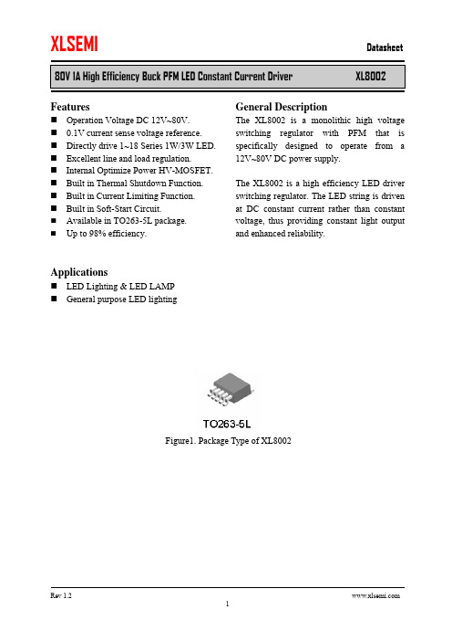
80V 1A High Efficiency Buck PFM LED Constant Current Driver XL8002FeaturesOperation Voltage DC 12V~80V. 0.1V current sense voltage reference. Directly drive 1~18 Series 1W/3W LED. Excellent line and load regulation.Internal Optimize Power HV-MOSFET. Built in Thermal Shutdown Function. Built in Current Limiting Function.Built in Soft-Start Circuit.Available in TO263-5L package. Up to 98% efficiency. ApplicationsLED Lighting & LED LAMP General purpose LED lightingGeneral DescriptionThe XL8002 is a monolithic high voltage switching regulator with PFM that is specifically designed to operate from a 12V~80V DC power supply.The XL8002 is a high efficiency LED driver switching regulator. The LED string is driven at DC constant current rather than constant voltage, thus providing constant light output and enhanced reliability.Figure1. Package Type of XL800280V 1A High Efficiency Buck PFM LED Constant Current Driver XL800280V 1A High Efficiency Buck PFM LED Constant Current Driver XL8002Figure4. XL8002 Typical Application80V 1A High Efficiency Buck PFM LED Constant Current Driver XL8002Figure5. Efficiency VS Output N*1W LEDFigure6. Output ILED Load Regulation VS Output N*1W LED80V 1A High Efficiency Buck PFM LED Constant Current Driver XL800280V 1A High Efficiency Buck PFM LED Constant Current Driver XL800280V 1A High Efficiency Buck PFM LED Constant Current Driver XL8002 Figure7. XL8002 System Application at VIN=60V~80V Schematic Figure8. XL8002 System Application at VIN=60V~80V Efficiency Curve80V 1A High Efficiency Buck PFM LED Constant Current Driver XL8002 Figure9. XL8002 System Application at VIN=36V~60V Schematic80V 1A High Efficiency Buck PFM LED Constant Current Driver XL8002Figure10. XL8002 System Application at VIN=36V~60V Efficiency Curve Table2: Figure9 Input VIN=36V/48V system parameters table:80V 1A High Efficiency Buck PFM LED Constant Current Driver XL8002Figure11. XL8002 System Application at VIN=12V~36V SchematicFigure12. XL8002 System Application at VIN=12V~36V Efficiency CurveTable3: Figure11 Input VIN=12V/24V system parameters table:VIN=12V VIN=24VFOSC Pout Efficiency FOSC Pout Efficiency1.01W 82.3%1.96W 90.8%2.91W 94.1%47.25K 3.80W 95.5%42.17K 4.70W 96.6%31.13K 5.61W 97.2%80V 1A High Efficiency Buck PFM LED Constant Current Driver XL8002 Figure13. XL8002 System Application at VIN=60V~80V Schematic Figure14. XL8002 System Application at VIN=60V~80V Efficiency Curve80V 1A High Efficiency Buck PFM LED Constant Current Driver XL800280V 1A High Efficiency Buck PFM LED Constant Current Driver XL8002。
LINEAR LTM8025 说明书

L DESIGN IDEASEasy LayoutThe LTM8025’s high level of integration simplifies the design of just about any 3A power supply. Just add two resis-tors, input and output capacitance to make a complete power supply. Layout is easy, as shown in Figure 1. Figures 2 and 3 show the schematic and ef-ficiency of the LTM8025 producing 12V bus power from a 24V source, while Figure 4 shows the LTM8025 producing 1.8V from an input range of 3.6V to 36V.Versatile Feature SetThe LTM8025 may be operated over a wide frequency, from 200kHz to 2.4MHz, and may be synchronized to an external clock source through the SYNC pin. The LTM8025 start-up is controlled through its RUN/SS pin, which also serves to put the part intoIntroductionAsk any group of engineers, “Whatwould you do with a 3A DC/DC con-verter?” and you will probably get a wide range of answers—from powering a DSP rail at 1.8V to running a bank of 24V switching I/O. Typically, these two particular applications would require completely different DC/DC controller ICs and topologies. How-ever, the LTM8025 µModule DC/DC converter can satisfy the requirements of these and just about any other 3A applications.The LTM8025 3A µModule DC/DC buck converter operates from 3.6V to 36V inputs to produce output voltages as low as 0.8V and as high as 24V. Furthermore, the LTM8025 features single cycle Burst Mode ® operation, so it is able to handle a wide range of load currents, from no load to 3A, with minimum ripple.Self-Contained 3A µModule Buck Regulator Produces 0.8V–24V Outputfrom 3.6V–36V InputV IN APPLICATIONS INFORMATION SECTION FOR START-UP DETAILSOUTµF Figure 2. A complete 12V at 3A power supply requires only the LTM8025, two capacitors and two resistors.OUTPUT CURRENT (mA)408060701009050E F F I C I E N C Y (%)050010001500200025003000Figure 3. The LTM8025 boasts high efficiency.V OUTµFFigure 4. The LTM8025 can produce low voltages from a wide input range.THERMAL VIAS TO GNDFigure 1. Layout is easy with the LTM8025.by David Ng The LTM8025 integrates the con-troller, control circuitry, inductor, power switch and rectifier all into a single IC form factor 15mm × 9mm × 4.32mm package. This LGA package is RoHS (e3) compliant, and features gold pads for easy assembly in both leaded and unleaded solder processes.continued on page 42L NEW DEVICE CAMEOSa low power off state in which the part draws less than 1µA. Furthermore, the part comes with a PGOOD pin to indicate that the output is within 90% of its target voltage.Parallel Multiple LTM8025s for High Current CapabilityThe LTM8025 is equipped with a SHARE pin to allow parallel operation for applications requiring more than 3A load current. Figure 5 shows two synchronized LTM8025’s providing 2.5V OUT at 5.6A.ConclusionThe highly versatile LTM8025 3A µModule DC/DC buck converter is easy to use and fits just about any step-down regulator need. Its wide input and output ranges and high level of integration reduce design effort and associated costs. LV IN *RUNNING VOL TAGE RANGE. PLEASE REFER TO APPLICATIONS INFORMATION SECTION FOR START-UP DETAILSNOTE: SYNCHRONIZE THE TWO MODULES TO AVOID BEAT FREQUENCIES,IF NECESSARY. OTHERWISE, TIE EACH SYNC TO GNDFigure 5. Two LTM8025s can be operated in parallel for more than 3A load current.LTM8025, continued from page 40The LT4356-2 is offered in 12-pin DFN and 16-pin SO packages, while the LT4356-3 is available in 12-pin DFN, 16-pin SO, and 10-pin MSOP packages.Dual Output Synchronous DC/DC Controller Draws Only 170µA in Battery-Powered SystemsThe LTC3868/-1 is a low quiescent current, 2-phase dual output synchro-nous step-down DC/DC controller. The LTC3868/-1 draws only 170µA with one output active and only 300µA when both outputs are active, making it ideal for battery-powered applica-tions. With both outputs shut down, the LTC3868/-1 draws only 8µA. The LTC3868/-1 has an input supply range of 4V to 24V and each output can be set from 0.8V to 14V at output cur-rents up to 20A. With efficiency as high as 95%, a LTC3868/-1 based DC/DC converter is well suited for powering industrial and medical devices, along with portable instruments, notebook and netbook computers.The LTC3868/-1 operates with a user-adjustable, fixed frequency between 50kHz and 900kHz, andcan be synchronized to an external clock from 75kHz to 850kHz using its phase-locked-loop (PLL). The user can select from continuous operation, pulse-skipping and low ripple Burst Mode operation during light loads. These parts also safely start up with a prebiased load by powering up and down in pulse-skipping mode.The LTC3868/-1’s 2-phase op-eration reduces input capacitance requirements and its current mode architecture provides easy loop com-pensation and fast transient response. Both outputs have adjustable soft-start to control the turn-on time, and the output overload protection feature latches off the converter until the input voltage is recycled. The LTC3868/ LTC3868-1 also features a tight ±1.5% reference voltage accuracy over a –40°C to 85°C operating temperature range. The LTC3868 is the fully fea-tured part with additional functions beyond the LTC3868-1 including a clock out, phase modulation, two power good outputs and adjustable current limit.The LTC3868 is offered in a 32-lead 5mm × 5mm QFN package and theLTC3868-1 in a 28-pin SSOP or 4mm × 5mm QFN-28 packages.Boost & Inverting DC/DC Converter for Active Matrix OLED & CCD BiasThe LT3582, LT3582-5 and LT3582-12 dual channel DC/DC converters that deliver both positive and negative outputs required in many biasing ap-plications such as active matrix OLED (organic light-emitting diode) displays as well as CCD (charge coupled device) applications. The LT3582/-5/-12 offer an I 2C interface that can dynamically program output voltages, power se-quencing and output voltage ramps as the application requires. Alternatively, these parameters can be set in manu-facturing and made permanent via the built in nonvolatile OTP (one time programmable) memory. The LT3582’s positive output voltage can be set be-tween 3.2V and 12.775 in 25mV steps, whereas the negative output can be set between –1.2V and –13.95V in 50mV steps. The LT3582-5 and LT3582-12 are pre-configured with ±5V and ±12V outputs respectively, useful in many signal conditioning applications. L。
具输出断接功能的1.5A、3MHz升压型转换器

3 MHz的恒定 开 关频 率最 大 限度
地 缩 小 了 电 感器 和 电容 器 尺 寸 . 提供 了 手持应 用 所需 的纤 巧解 决 方案 占板 面积 。
L C 4 2采 用 R T 32 DS( N) o 仅
P31 时 ,光量达 到 6 1 。采用脉 ; 驱 NC 5 8 的设计使 电源 管理 子系 4W 中
维普资讯
欧 司 朗推 出
动功能 。其 内部开 关提 供 1 A 电 . 5 流限制 ( 最小) 并在05 . V~45 .V的 输 入 电压 范 围提 供 高达 52 V的 .5
白色 L D光效达 4 1 W E 0 m/
德 国欧 司朗光 电 半导体 公 司
路保 护 、 编程软 启动 和热保护 。 可 采 用 1 引线 DFN 封 装 的 0
源管理的双缘控 制器
凌特公 司推 出 3 MHz 、电流
L C 4 2 DD每 片起价 为 29 T 32 E . 5美
元。
●
安森 美半 导体 推 出异步 双缘 模式 、 同步 升压型 DC D / C转 换器 (u l d e 脉 冲宽度调 制 (WM) L C 4 2 d a- g ) e P T 3 2 .该器 件具 有真 正输 出 控 制器 N P 3 。这全新 控制器 断接 、3 3 电流 限制 和集 成软 启 C 58 1 ti  ̄l i
成 白色 。
少外 部 元件 .因此 比现 有解 决方 制 了启动 时 的浪涌 电流 .最大 限
法 的性价 比更高 。
度 地 降低 了输入 电源端 的 浪涌 电
流 。 它特点 包括 防振 铃控 制、 其 短
具输 出断接功能的 1 5 .A
怎样采用一个μModule降压型稳压器从正输入产生负输出电压

怎样采用一个μModule降压型稳压器从正输入产生负输出电压如图1所示,通过将传统的降压型μModule?稳压器配置成一个负输出降压-升压型转换器,即可轻松地使其产生负输出电压。
输入电源的负端连接至μModule稳压器的VOUT引脚,而GND引脚则连接至-VOUT电源轨。
μModule稳压器所承受的实际输入电压(VIN’)为输入电源(VIN)与输出电压(-VOUT)的压差。
该电压必须处在器件的可容许输入范围之内。
此外,输出电压的绝对值一定不得超过μModule稳压器的最大额定输出电压。
由于器件现在的作用是一个负输出降压-升压型转换器,因此其开关电流大于同类的降压型转换器。
于是,必须考虑使诸如输出电流、开关频率、热性能等参数保持在器件的限值范围以内。
图1a:为产生正输出电压而配置的降压型μModule稳压器 图1b:为产生负输出电压而配置的降压型μModule稳压器 -12V输出应用 LTM8025是一款36VIN、3A降压型μModule转换器,能够支持高达24V的输出电压。
可轻松地通过配置使其产生负输出电压,而为此所需承担的设计工作量极少。
图2示出了LTM8025从一个20V至24V的输入范围产生-12V/2A输出的电路原理图。
LTM8025所承受的实际输入电压为VIN’=VIN-(-VOUT)。
例如:若VIN=20V,则VIN’=20V-(-12V)=32V。
由于LTM8025的最大额定输入为36V,因此该特定应用电路中的输入电源被限制为24V。
图2:针对-12V输出的LTM8025应用电路原理图 此外,通过把一个250kHz至2MHz的外部时钟信号施加至SYNC引脚,可对LTM8025的内部振荡器进行同步处理。
对于负输出电压,必须对时钟进行。
LTM8025EV#PBF;LTM8025IV#PBF;LTM8025MPV#PBF;DC1379A;中文规格书,Datasheet资料

18025faT YPICAL APPLICATIONF EATURESA PPLICATIONSD ESCRIPTION µModule RegulatorThe L TM ®8025 is a 36V IN , 3A step down μModule ® con-verter . Included in the package are the switching controller , power switches, inductor and all support components. Operating over an input voltage range of 3.6V to 36V , the L TM8025 supports an output voltage range of 0.8V to 24V and a switching frequency range of 200kHz to 2.4MHz, each set by a single resistor . Only the bulk input and output fi lter capacitors are needed to fi nish the design.The low profi le package (4.32mm) enables utilization of unused space on the bottom of PC boards for high density point of load regulation.The L TM8025 is packaged in a thermally enhanced, compact (15mm × 9mm) and low profi le (4.32mm) over-molded land grid array (LGA) package suitable for automated assembly by standard surface mount equipment. The L TM8025 is RoHS compliant.L , L T , L TC, L TM, Linear Technology, the Linear logo, μModule and Burst Mode are registered trademarks of Linear Technology Corporation. All other trademarks are the property of their respective owners.nComplete Step-Down Switch Mode Power Supply n Wide Input Voltage Range: 3.6V to 36V n Up to 3A Output Currentn Parallelable for Increased Output Current n 0.8V to 24V Output Voltagen Selectable Switching Frequency: 200kHz to 2.4MHz n Current Mode Controln (e4) RoHS Compliant Package with Gold Pad Finish n Programmable Soft-Start n Tiny, Low Profi le (15mm × 9mm × 4.32mm) Surface Mount LGA PackagenAutomotive Battery Regulation n Power for Portable Products n Distributed Supply Regulation n Industrial Supplies n Wall T ransformer RegulationEffi ciencyOUTPUT CURRENT (mA)4080607010090508025 TA01bE F F I C I E N C Y (%)0500100015002000250030008025 TA01aV IN APPLICATIONS INFORMATION SECTION FOR START-UP DETAILSV OUT12V AT 3AμF/28025faA BSOLUTE MAXIMUM RATINGS V IN , RUN/SS Voltage .................................................36V ADJ, RT, SHARE Voltage .............................................6V V OUT , AUX .................................................................25V PGOOD, SYNC...........................................................30V BIAS .. (25V)V IN + BIAS.................................................................56V Maximum Junction Temperature (Note 2) ............125°C Solder Temperature ...............................................245°C(Note 1)ORDER INFORMATIONP IN CONFIGURATIONE LECTRICAL CHARACTERISTICS Thel denotes the specifi cations which apply over the full operating temperature range, otherwise specifi cations are at T A = 25°C. V IN = 12V , RUN/SS = 12V , BIAS = 3V unless otherwise noted. (Note 2)PARAMETER CONDITIONSMINTYP MAX UNITSMinimum Input Voltage l3.6V Output DC Voltage 0 < I OUT ≤ 3A; R ADJ Open0 < I OUT ≤ 3A; R ADJ = 16.9k; V IN = 32V 0.824V V Output DC Current V OUT = 3.3V3A Quiescent Current into V INRUN/SS = 0V Not SwitchingBIAS = 0V , Not Switching 0.012585160150μA μA μA Quiescent Current into BIASRUN/SS = 0V Not SwitchingBIAS = 0V , Not Switching 0.016500.51205μA μA μA Line Regulation 5.5V < V IN < 36V , I OUT = 1A 0.3%Load Regulation0A < I OUT < 3A0.4%LEAD FREE FINISH TRAYPART MARKING PACKAGE DESCRIPTIONTEMPERATURE RANGE L TM8025EV#PBF L TM8025EV#PBF 8025V 70-Lead (15mm × 9mm × 4.32mm) LGA –40°C to 125°C L TM8025IV#PBF L TM8025IV#PBF 8025V 70-Lead (15mm × 9mm × 4.32mm) LGA –40°C to 125°C L TM8025MPV#PBFL TM8025MPV#PBF8025MPV70-Lead (15mm × 9mm × 4.32mm) LGA–55°C to 125°CConsult L TC Marketing for parts specifi ed with wider operating temperature ranges.For more information on lead free part marking, go to: http://www.linear .com/leadfree/This product is only offered in trays. For more information go to: http://www.linear .com/packaging//38025faE LECTRICAL CHARACTERISTICS Note 1: Stresses beyond those listed under Absolute Maximum Ratings may cause permanent damage to the device. Exposure to any Absolute Maximum Rating condition for extended periods may affect device reliability and lifetime.Note 2: The L TM8025E is guaranteed to meet performance specifi cations from 0°C to 125°C internal. Specifi cations over the full –40°C to 125°C internal operating temperature range are assured by design,PARAMETERCONDITIONS MINTYP MAXUNITS Output Voltage Ripple (RMS)0A < I OUT < 3A 10mV Switching Frequency R T = 45.3k 775kHz Voltage (at ADJ Pin)l775770790805810mV mV Current Out of ADJ PinADJ = 1V , V OUT = 0V 2μA Minimum BIAS Voltage for Proper Operation2 2.8V RUN/SS Pin Current RUN/SS = 2.5V 510μA RUN Input High Voltage2.5V RUN Input Low Voltage 0.2V PGOOD Threshold (at ADJ Pin)V OUT Rising 710mV PGOOD Leakage Current PGOOD = 30V 0.11μA PGOOD Sink Current PGOOD = 0.4V 200700μA SYNC Input Low Threshold f SYNC = 550kHz 0.5V SYNC Input High Threshold f SYNC = 550kHz 0.7V SYNC Bias CurrentSYNC = 0V0.1μAThe l denotes the specifi cations which apply over the full operatingtemperature range, otherwise specifi cations are at T A = 25°C. V IN = 12V , RUN/SS = 12V , BIAS = 3V unless otherwise noted. (Note 2)characterization and correlation with statistical process controls. The L TM8025I is guaranteed to meet specifi cations over the full –40°C to 125°C internal operating temperature range. The L TM8025MP is guaranteed to meet specifi cations over the full –55°C to 125°C internal operating temperature range. Note that the maximum internal temperature is determined by specifi c operating conditions in conjunction with board layout, the rated package thermal resistance and other environmental factors./48025fa408060701009050E F F I C I E N C Y (%)500100015002000250030008025 G04LOAD CURRENT (mA)T YPICAL PERFORMANCE CHARACTERISTICS 2.5V OUT Effi ciency3.3V OUT Effi ciency5V OUT Effi ciency8V OUT Effi ciency12V OUT Effi ciency18V OUT Effi ciencyBias Current vs Load Current 2.5V OUTBias Current vs Load Current 3.3V OUTBias Current vs Load Current 5V OUT408060701009050E F F I C I E N C Y (%)500100015002000250030008025 G01LOAD CURRENT (mA)408060701009050E F F I C I E N C Y (%)500100015002000250030008025 G02LOAD CURRENT (mA)408060701009050E F F I C I E N C Y (%)500100015002000250030008025 G03LOAD CURRENT (mA)408060701009050E F F I C I E N C Y (%)500100015002000250030008025 G05LOAD CURRENT (mA)408060701009050E F F I C I E N C Y (%)500100015002000250030008025 G06LOAD CURRENT (mA)8025 G07LOAD CURRENT (mA)525201510B I A SC U R R E N T (m A )1000200030008025 G08LOAD CURRENT (mA)53025201510B I A S C U R R E N T (m A)1000200030008025 G09LOAD CURRENT (mA)540352520301510B I A S C U R R E N T (m A )100020003000T A = 25°C, unless otherwise noted./58025faTYPICAL PERFORMANCE CHARACTERISTICSBias Current vs Load Current 8V OUTBias Current vs Load Current 12V OUTBias Current vs Load Current 18V OUTInput Current vs Load Current 2.5V OUTInput Current vs Load Current 3.3V OUTInput Current vs Load Current 5V OUTInput Current vs Load Current 8V OUTInput Current vs Load Current 12V OUTInput Current vs Load Current 18V OUT8025 G10LOAD CURRENT (mA)08070605040203010B I A S C U R R E N T (m A )1000200030008025 G11LOAD CURRENT (mA)B I A SC U R R E N T (m A )100020003000706050402030108025 G12LOAD CURRENT (mA)12010080604020B I A S C U R R E N T (m A )500100015008025 G13LOAD CURRENT (mA)5002500200015001000I N P U T C U R R E N T (m A )1000200030008025 G14LOAD CURRENT (mA)5002500200015001000I N P U T C U R R E N T (m A )1000200030008025 G15LOAD CURRENT (mA)4006008002001600140012001000I N P U T C U R R E N T (m A )1000200030008025 G16LOAD CURRENT (mA)5002500200015001000I N P U T C U R R E N T (m A )1000200030008025 G17LOAD CURRENT (mA)50030002500200015001000I N P U T C U R R E N T (m A )1000200030008025 G18LOAD CURRENT (mA)50030002500200015001000I N P U T C U R R E N T (m A )100020003000T A = 25°C, unless otherwise noted./68025fa8025 G22LOAD CURRENT (mA)4.06.57.57.06.05.55.04.5I N P U T V O L T A G E (V )100020003000T YPICAL PERFORMANCE CHARACTERISTICS Input Current vs Input VoltageOutput ShortedMinimum Input Running Voltage vs V OUT , I OUT = 3AMinimum Input Voltage vs Load Current, 3.3V OUTMinimum Input Voltage vs Load Current, 5V OUTMinimum Input Voltage vs Load Current, 8V OUTMinimum Input Voltage vs Load Current, 12V OUTMinimum Input Voltage vs Load Current, 18V OUTMinimum Input Voltage vs Load Current, –3.3V OUTMinimum Input Voltage vs Load Current, –5V OUTINPUT VOL TAGE (V)I N P U T C U R R E N T (m A )60050030020010040008025 G19201030OUTPUT VOL TAGE (V)01I N P U T V O L T A G E (V )40353020102515514710118025 G2015129813532648025 G21LOAD CURRENT (mA)3.03.56.05.55.04.54.0I N P U T V O L T A G E (V )1000200030008025 G25LOAD CURRENT (mA)1232271722I N P U T V O L T A G E (V )1000200030008025 G26LOAD CURRENT (mA)12345671098I N P U T V O L T A G E (V )1000200030008025 G27LOAD CURRENT (mA)1014128642I N P U T V O L T A G E (V )100020003000T A = 25°C, unless otherwise noted.8025 G23LOAD CURRENT (mA)8.010.511.010.09.59.08.5I N P U T V O L T A G E (V )1000200030008025 G24LOAD CURRENT (mA)1213141516171819222120I N P U T V O L T A G E (V )100020003000/78025fa8025 G31LOAD CURRENT (mA)051510453530254020T E M P E R A T U R E R I S E (°C )500100015002000250030003500T YPICAL PERFORMANCE CHARACTERISTICS Minimum Input Voltage vs LoadCurrent, –8V OUTMinimum Input Voltage vs Load Current, –12V OUTMinimum Input Voltage vs Negative V OUTJunction Temperature Rise vs Load Current, 2.5V OUTJunction Temperature Rise vs Load Current, 3.3V OUTJunction Temperature Rise vs Load Current, 5V OUTJunction Temperature Rise vs Load Current, 8V OUTJunction Temperature Rise vs Load Current, 12V OUTJunction Temperature Rise vs Load Current, 18V OUT8025 G28LOAD CURRENT (mA)5101520I N P U T V O L T A G E (V )1000200030008025 G29LOAD CURRENT (mA)25302015105I N P U T V O L T A G E (V )1000200030008025 G13OUTPUT VOL TAGE (V)525201510I N P U T V O L T A G E (V )–5–10–155001000150020002500300035008025 G32106050304020T E MP E R A T U R E R I S E (°C )LOAD CURRENT (mA)5001000150020002500300035008025 G33LOAD CURRENT (mA)5151050453530254020T E M P E R A T U R E R I S E (°C )8025 G34LOAD CURRENT (mA)01080706050304020T E M P E R AT U R E R I S E (°C )500100015002000250030003500T A = 25°C, unless otherwise noted.8025 G35LOAD CURRENT (mA)12010080604020T E M P E R A T U R E R I S E (°C )0500100015002000250030008025 G36LOAD CURRENT (mA)10080604020T E M P E R A T U R E R I S E (°C )0500100015002000/P IN FUNCTIONSV OUT (Bank 1): Power Output Pins. Apply the output fi lter capacitor and the output load between these pins and GND pins.GND (Bank 2): Tie these GND pins to a local ground plane below the LTM8025 and the circuit components. In most applications, the bulk of the heat fl ow out of the LTM8025 is through these pads, so the printed circuit design has a large impact on the thermal performance of the part. See the PCB Layout and Thermal Considerations sections for more details. Return the feedback divider (R ADJ) to this net.V IN (Bank 3): The V IN pin supplies current to the L TM8025’s internal regulator and to the internal power switch. This pin must be locally bypassed with an external, low ESR capacitor; see Table 1 for recommended values.AUX (Pin G5): Low Current Voltage Source for BIAS. In many designs, the BIAS pin is simply connected to V OUT. The AUX pin is internally connected to V OUT and is placed adjacent to the BIAS pin to ease printed circuit board rout-ing. Although this pin is internally connected to V OUT, it is not intended to deliver a high current, so do not draw current from this pin to the load. If this pin is not tied to BIAS, leave it fl oating.BIAS (Pin H5): The BIAS pin connects to the internal power bus. Connect to a power source greater than 2.8V and less than 25V. If the output is greater than 2.8V, connect this pin there. If the output voltage is less, connect this to a voltage source between 2.8V and 25V. Also, make sure that BIAS + V IN is less than 56V.RUN/SS (Pin L5): Pull the RUN/SS pin below 0.2V to shut down the L TM8025. Tie to 2.5V or more for normal operation. If the shutdown feature is not used, tie this pin to the V IN pin. RUN/SS also provides a soft-start function; see the Applications Information section.SYNC (Pin L6): This is the external clock synchronization input. Ground this pin for low ripple Burst Mode operation at low output loads. Tie to a stable voltage source greater than 0.7V to disable Burst Mode operation. Do not leave this pin fl oating. Tie to a clock source for synchroniza-tion. Clock edges should have rise and fall times faster than 1μs. See the Synchronization section in Applications Information.RT (Pin G7): The RT pin is used to program the switching frequency of the L TM8025 by connecting a resistor from this pin to ground. Table 2 gives the resistor values that correspond to the resultant switching frequency. Minimize the capacitance at this pin.SHARE (Pin H7): Tie this to the SHARE pin of another L TM8025 when paralleling the outputs. Otherwise, do not connect.PGOOD (Pin J7): The PGOOD pin is the open-collector output of an internal comparator. PGOOD remains low until the ADJ pin is within 10% of the final regulation voltage. PGOOD output is valid when V IN is above 3.6V and RUN/SS is high. If this function is not used, leave this pin fl oating.ADJ (Pin K7): The L TM8025 regulates its ADJ pin to 0.79V. Connect the adjust resistor from this pin to ground. The value of R ADJ is given by the equation R ADJ = 394.21/(V OUT – 0.79), where R ADJ is in kΩ./88025faB LOCK DIAGRAM O PERATIONThe L TM8025 is a standalone nonisolated step-down switching DC/DC power supply that can deliver up to 3A of output current. This module provides a precisely regulated output voltage programmable via one external resistor from 0.8V to 25V. The input voltage range is 3.6V to 36V. Given that the L TM8025 is a step-down converter, make sure that the input voltage is high enough to support the desired output voltage and load current.As shown in the Block Diagram, the L TM8025 contains a current mode controller, power switching element, power inductor, power Schottky diode and a modest amount of input and output capacitance. The L TM8025 is a fi xed frequency PWM regulator. The switching frequency is set by simply connecting the appropriate resistor value from the RT pin to GND.An internal regulator provides power to the control circuitry. The bias regulator normally draws power from the V IN pin, but if the BIAS pin is connected to an external volt-age higher than 2.8V, bias power will be drawn from the external source (typically the regulated output voltage). This improves effi ciency. The RUN/SS pin is used to place the L TM8025 in shutdown, disconnecting the output and reducing the input current to less than 1μA.To further optimize effi ciency, the L TM8025 automatically switches to Burst Mode® operation in light load situations. Between bursts, all circuitry associated with controlling the output switch is shut down reducing the input supply current to 50μA in a typical application.The oscillator reduces the L TM8025’s operating frequency when the voltage at the ADJ pin is low. This frequency foldback helps to control the output current during start-up and overload.The L TM8025 contains a power good comparator which trips when the ADJ pin is at roughly 90% of its regulated value. The PGOOD output is an open-collector transistor that is off when the output is in regulation, allowing an external resistor to pull the PGOOD pin high. Power good is valid when the L TM8025 is enabled and V IN is above 3.6V. The L TM8025 is equipped with a thermal shutdown that will inhibit power switching at high junction tempera-tures. The activation threshold of this function, however, is above 125°C to avoid interfering with normal operation. Thus, prolonged or repetitive operation under a condition in which the thermal shutdown activates may damage or impair the reliability of the device./98025faA PPLICATIONS INFORMATIONF or most applications, the design process is straight forward, summarized as follows:1. Look at Table 1 and fi nd the row that has the desired input range and output voltage.2. Apply the recommended C IN, C OUT, R ADJ and R T values.3. Connect BIAS as indicated.While these component combinations have been tested for proper operation, it is incumbent upon the user to verify proper operation over the intended system’s line, load and environmental conditions. Bear in mind that the maximum output current is limited by junction tempera-ture, the relationship between the input and output voltage magnitude and polarity and other factors. Please refer to the graphs in the Typical Performance Characteristics section for guidance.The maximum frequency (and attendant R T value) at which the L TM8025 should be allowed to switch is given in Table 1 in the f MAX column, while the recommended frequency (and R T value) for optimal effi ciency over the given input condition is given in the f OPTIMAL column. There are additional conditions that must be satisfi ed if the synchronization function is used. Please refer to the Synchronization section for details.Capacitor Selection ConsiderationsThe C IN and C OUT capacitor values in Table 1 are the minimum recommended values for the associated oper-ating conditions. Applying capacitor values below those indicated in Table 1 is not recommended, and may result in undesirable operation. Using larger values is generally acceptable, and can yield improved dynamic response, if it is necessary. Again, it is incumbent upon the user to verify proper operation over the intended system’s line, load and environmental conditions.Ceramic capacitors are small, robust and have very low ESR. However, not all ceramic capacitors are suitable. X5R and X7R types are stable over temperature and ap-plied voltage and give dependable service. Other types, including Y5V and Z5U have very large temperature and voltage coeffi cients of capacitance. In an application cir-cuit they may have only a small fraction of their nominal capacitance resulting in much higher output voltage ripple than expected.Ceramic capacitors are also piezoelectric. In Burst Mode operation, the L TM8025’s switching frequency depends on the load current, and can excite a ceramic capacitor at audio frequencies, generating audible noise. Since the L TM8025 operates at a lower current limit during Burst Mode operation, the noise is typically very quiet to a casual ear.If this audible noise is unacceptable, use a high perfor-mance electrolytic capacitor at the output. It may also be a parallel combination of a ceramic capacitor and a low cost electrolytic capacitor.A fi nal precaution regarding ceramic capacitors concerns the maximum input voltage rating of the L TM8025. A ceramic input capacitor combined with trace or cable inductance forms a high Q (under damped) tank circuit. If the L TM8025 circuit is plugged into a live supply, the input voltage can ring to twice its nominal value, possi-bly exceeding the device’s rating. This situation is easily avoided; see the Hot-Plugging Safely section. Frequency SelectionThe L TM8025 uses a constant frequency PWM architec-ture that can be programmed to switch from 200kHz to 2.4MHz by using a resistor tied from the RT pin to ground. Table 2 provides a list of R T resistor values and their re-sultant frequencies./108025fa分销商库存信息:LINEAR-TECHNOLOGYLTM8025EV#PBF LTM8025IV#PBF LTM8025MPV#PBF DC1379A。
5V转3.3V,3V,2.8V,1.8V降压2A芯片电路-PW2051

PW2051 是一款由基准电压源、振荡电路、比较器、 PWM/PFM 控制电路等构成的 CMOS 降压型 DC/DC 调整器。
利用 PWM/PFM 自动切换控制电路达到可调占空比,具有全输入电压范围内的低纹波、高效率和大输出电流等特点。
PW2051 内置功率 MOSFET,集成了过压、过流、过热、 短路等诸多保护电路,在超过控制值时会自动断开,以保护芯片。
本产品结合了微型封装和低消耗电流等特点,最适合在移动设备的电源内部使用。
PW2051采用SOT23-5L封装配合较少的外围原件使其非常适用于便携式产品.产品特点●最大效率可达 95%●最大输出电流 1.5A●超低静态电流 40μA●甚小输出纹波 <±0.4%●低压操作 可达 100%占空比●PWM/PFM 自动切换 占空比自动可调以保持全负载范围内的高效率、低纹波●短路保护应用范围●数码相机、电子记事本、 PDA 等移动设备电源●照相机、视频设备、通信设备的稳压电源●微机电源●机顶盒典型应用电路C1为可选电容引脚配置/说明引脚号符号 引脚说明 1CE 芯片使能端,高有效 2GND 地 3LX 内部功率开关输出端口 4VIN 电源输入端 5 FB 输出电压反馈端绝对最大额定值 项目符号 绝对最大额定值 单位 输入电压VIN -0.3~6.5V 输出电压VFB -0.3~6.5 V VLX -0.3~VIN + 0.3 V CE 端电压VCE -0.3~VIN + 0.3 V LX 端电流ILX ±2 A 容许功耗Pd 250 mW 工作环境温度Topr -40~+85 ℃ 保存温度 Tstg -55~+125 ℃CE GND LX FB SOT-23-5L (TOP VIEW)VIN 12345PCB 布局为了使噪音最低和操作性能最佳, PCB 布局时以下几点建议可作为参考:1、 VIN、 LX 、 GND 组成的功率通路,尽量采用短而宽的布线,避免过孔。
- 1、下载文档前请自行甄别文档内容的完整性,平台不提供额外的编辑、内容补充、找答案等附加服务。
- 2、"仅部分预览"的文档,不可在线预览部分如存在完整性等问题,可反馈申请退款(可完整预览的文档不适用该条件!)。
- 3、如文档侵犯您的权益,请联系客服反馈,我们会尽快为您处理(人工客服工作时间:9:00-18:30)。
LTM8025 - 36V、3A 降压型μModule转换器
描述:
LTM®8025是一款36VIN、3A 降压型μModule®转换器。
封装中内置了开关控制器、电源开关、电感器以及所有的支持元件。
LTM8025 可一个在3.6V 至36V 的输入电压范围内运作,支持一个0.8V 至24V 的输出电压范围和一个200kHz 至 2.4MHz 的开关频率范围(各由单个电阻器来设定)。
仅需采用大容量的输入和输出滤波电容器便可实现完整的设计。
由于采用了扁平的封装(高度仅 4.32mm),因而可以利用PC 板底部的未用空间,以实现高密度负载点调节。
LTM8025 采用耐热增强型的紧凑(15mm x 9mm)、扁平(高度仅4.32mm) 模压树脂焊盘网格阵列(LGA) 封装,适合采用标准的表面贴装设备来进行自动化装配。
LTM8025 符合RoHS 标准。
特点:
·完整的降压型开关模式电源
·宽输入电压范围:3.6V 至36V
·高达3A 的输出电流
·可通过并联来增加输出电流
·0.8V至24V 输出电压范围
·可选开关频率:200kHz 至2.4MHz
·电流模式控制
·具有金制衬垫涂层并符合RoHS 标准的无铅型(e4) 封装
·可编程软起动
·纤巧和扁平(15mm x 9mm x 4.32mm) 的表面贴装型LGA 封装。