nRF24LE1 功率扩展 使用RFX2401芯片(集成PA LAN Switch)
Skyworks Solutions RFX2401C数据手册说明书
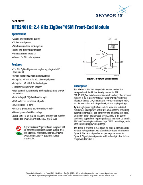
DATA SHEETRFX2401C: 2.4 GHz ZigBee ®/ISM Front-End ModuleApplications∙ ZigBee extended range devices ∙ ZigBee smart power∙ Wireless sound and audio systems ∙ Home and industrial automation ∙ Wireless sensor networks ∙ Custom 2.4 GHz radio systemsFeatures∙ 2.4 GHz ZigBee high-power single-chip, single-die RF front-end IC∙ Single-ended 50 Ω input and output ports ∙ Integrated PA with up to +22 dBm output power ∙ Integrated LNA with 2.5 dB noise figure ∙ Transmit/receive switch circuitry∙ High transmit signal linearity meeting standards for OQPSK modulation∙ Low voltage (1.2 V) CMOS control logic ∙ ESD protection circuitry on all ports ∙ DC decoupled RF ports∙ Full on-chip matching and decoupling circuitry ∙ Market proven CMOS technology∙ Small QFN, 16-pin (3 x 3 x 0.55 mm) package with exposed ground pad (MSL1, 260 ︒C per JEDEC J-STD-020)S kywork s G reen™ product s are compliant with all applicable legi s lation and are halogen-free.For additional information, refer to Skyworks Definition of Green™, document number S Q04-0074.204359-001Figure 1. RFX2401C Block DiagramDescriptionThe RFX2401C is a fully integrated front-end module that incorporates all the RF functionality needed for IEEE802.15.4/ZigBee, wireless sensor network, and any other wireless systems in the 2.4 GHz ISM band. The RFX2401C architecture integrates the PA, LNA, transmit and receive switching circuitry, and the associated matching network, all in a single package. Typical high-power applications include home and industrial automation, smart power, and RF4CE among others. Combining superior performance, high sensitivity and efficiency, low noise, small form factor, and low cost, the RFX2401C is the perfect solution for applications requiring extended range and bandwidth. RFX2401C has simple and low-voltage CMOS control logic, and a wide operating supply voltage range.The device is provided in a compact, 16-pin 3 x 3 mm Quad Flat No-Lead (QFN) package. A functional block diagram is shown in Figure 1. The pin configuration and package are shown inFigure 2. Signal pin assignments and functional pin descriptions are provided in Table 1.204359-002N/C G ND G ND TXRX TXENN/CVDD N/CG ND ANTG NDRXENN/C DN C VDD G ND1651234151413678910111217G NDFigure 2. RFX2401C Pinout(Top View)Table 1. RFX2401C Signal DescriptionsPin Name DescriptionPin Name Description1 N/C Not connected internally 9 GND Ground2GNDGround 10ANTConnect to 50 Ω antenna (DC shorted to GND) 3 GND Ground11 GND Ground4 TXRX RF signal to/from the transceiver (DC shorted to GND) 12 N/C Not connected internally5 TXEN CMOS input to control TX enable 13 DNC Do not connect6 RXEN CMOS input to control RX enable 14 VDD Alternate supply pin, internally connected to pin 167 N/C Not connected internally 15 N/C Not connected internally 8GNDGround16VDDVoltage supply connectionElectrical and Mechanical SpecificationsThe absolute maximum ratings of the RFX2401C are provided in Table 2. The recommended operating conditions are specified in Table 3. The electrical specifications are provided in Tables 4 and 5. The state of the RFX2401C is determined by the logic provided in Table 6.Table 2. RFX2401C Absolute Maximum Ratings1Parameter Conditions Minimum Maximum Units DC VDD voltage supply 0 4.0 VDC control pin voltage Through 1 kΩ resistor 0 3.6 VDC VDD current consumption Through VDD pins when TX is “ON” 350 mADC control pin current consumption 1 μATX RF input power All operating modes +5 dBmANT RF input power When RX is “ON” +5 dBmJunction temperature 150 °CStorage ambient temperature No RF and DC voltages applied -50 +150 o CElectrostatic discharge:Human Body Model (HBM) 3250 V 1Exposure to maximum rating conditions for extended periods may reduce device reliability. There is no damage to device with only one parameter set at the limit and all other parameters set at or below their nominal value. Exceeding any of the limits listed here may result in permanent damage to the device. All maximum RF input power ratings assume 50 Ω terminalimpedance.ESD HANDLING: Although this device is designed to be as robust as possible, electrostatic discharge (ESD) can damage this device.This device must be protected at all times from ESD when handling or transporting. Static charges may easily producepotentials of several kilovolts on the human body or equipment, which can discharge without detection.Industry-standard ESD handling precautions should be used at all times.Table 3. RFX2401C Recommended Operating Conditions1Parameter Conditions Min Typ Max Units DC VDD voltage supply All VDD pins 2.0 3.3 3.6 VControl voltage “high” Through 1 kΩ resistor 1.2 VDD VControl voltage “low” 0 0.3 VOperating ambient temperature Note 2 -40 +125o Cθja35o C/W1 During production test, devices will be tested at 5 V.2 For operation above +85 °C, use the θ ja as guidance for system design to assure the junction temperature will not exceed the maximum of +150 °C.Table 4. RFX2401C Electrical Specifications1 (V DD = 3.3 V, All Unused Ports Terminated with 50 Ω, T A = 25 °C, Unless Otherwise Noted) Parameter Symbol Test Condition Min Typ Max Units Frequency range f 2.4 2.525 GHz Transmit ModeSaturated output power +22 dBm Small-signalgain 21.5 25 26.5 dBSecond harmonic P OUT = +20 dBm, IEEE 802.15.4OQPSK modulation signal–10 dBm/MHzThird harmonic P OUT = +20 dBm, IEEE 802.15.4OQPSK modulation signal–20 dBm/MHzInput return loss –10 dBOutputreturnloss –6 dB Input / output impedance single-ended 50 ΩTX quiescent current No RF applied 17 mATX high-power current P OUT = +20 dBm 90 mALoad VSWR for stability (P OUT = +20 dBm) All non-harmonically related spursless than –43 dBm/MHz6:1 N/ALoad VSWR for ruggedness(P OUT = +20 dBm)No damage 10:1 N/A Receive ModeGain 12 dB Noisefigure 2.5 dB Input return loss –10 dBOutput return loss –12 dBRf port impedance 50 ΩRx quiescent current No RF applied 8 mAInput p1db At ANT pin –8 dBm1 Performance is guaranteed only under the conditions listed in this table.Table 5. RFX2401C Standby Mode Technical ParametersParameter Symbol Test Condition Min Typ Max Units DC shutdown current 1 μATXRX-ANT insertion loss (S21) Pin < -20 dBm –50 dBANT-TXRX insertion loss (S21) –50 dBReturn loss (S11) From TXRX port –1.5 dBTransmit-receive switchingtime 800 nsec Shutdown and “ON” State switchingtime 800 nsecTable 6. RFX2401C Control Logic1Mode TXEN RXENTX active 1 xRX active 0 1Shutdown 00 1 “1” denotes high voltage state (> 1.2 V)“0” denotes low voltage stage (< 0.3 V) at control pins“X” denotes do not care: either “1” or “0” can be appliedApplication Schematic Board DescriptionA suggested RFX2401C FEM application schematic diagram is shown in Figure 3. A schematic of the Evaluation Board is shown in Figure 4.Circuit Design ConsiderationsThe following design considerations are general in nature and must be followed regardless of final use or configuration:∙Paths to ground should be made as short as possible.∙If the transceiver TXRX port has DC present, use a capacitor to block this voltage from reaching the RFX2401C.∙The ground pad of the RFX2401C has special electrical and thermal grounding requirements. This pad is the main thermal conduit for heat dissipation. Because the circuit board acts as the heat sink, it must shunt as much heat as possible from the device.Multiple vias to the grounding layer are e thermal vias to assure efficient heat dissipation. ∙Locate the bypass capacitors as close as possible to the ground pad. Use two ground vias.∙The VDD (pin 14) is an optional VDD pin, internally connected to pin 16.∙The N/C pins 1, 7, 12, and 15 may be left open or connected to GND.∙If the antenna circuits have DC present, use a capacitor to block this voltage from reaching the RFX2401C.NOTE: A poor connection between the ground pad and ground increases junction temperature (T J), which reduces the lifeof the device..J4Figure 3. RFX2401C Application SchematicMA J2SFigure 4. RFX2401C Evaluation Board SchematicPackage DimensionsThe PCB layout footprint for the RFX2401C is shown in Figure 5. Typical part markings are shown in Figure 6. Package dimensions are shown in Figure 7, and tape and reel dimensions are provided in Figure 8.Package and Handling InformationInstructions on the shipping container label regarding exposure to moisture after the container seal is broken must be followed. Otherwise, problems related to moisture absorption may occur when the part is subjected to high temperature during solder assembly.The RFX2401C is rated to Moisture Sensitivity Level 1 (MSL1) at 260 C. It can be used for lead or lead-free soldering. For additional information, refer to the Skyworks Application Note, Solder Reflow Information , document number 200164. Care must be taken when attaching this product, whether it is done manually or in a production solder reflow environment. Production quantities of this product are shipped in a standard tape and reel format.204359-0040.5mm0.25mmFigure 5. RFX2401C PCB Layout Footprint(Top View)204359-006S kywork s Part Number Lot C odeDate C odePin 1Figure 6. Typical Part Markings(Top View)9-007Figure 7. RFX2401C Package DimensionsAll measurements are in millimeters.204359-0083.30 ±0.10Figure 8. RFX2401C Tape and Reel DimensionsDATA SHEET • RFX2401C: 2.4 GHz ZIGBEE/ISM FRONT-END MODULEOrdering InformationModel Name Manufacturing Part Number Evaluation Board Part Number RFX2401C: 2.4 GHz ZigBee/ISM Front-End Module RFX2401C RFX2401C-EK1Copyright © 2016-2017 Skyworks Solutions, Inc. All Rights Reserved.Information in this document is provided in connection with Skyworks Solutions, Inc. (“Skyworks”) products or services. These materials, including the information contained herein, are provided by Skyworks as a service to its customers and may be used for informational purposes only by the customer. Skyworks assumes no responsibility for errors or omissions in these materials or the information contained herein. Skyworks may change its documentation, products, services, specifications or product descriptions at any time, without notice. Skyworks makes no commitment to update the materials or information and shall have no responsibility whatsoever for conflicts, incompatibilities, or other difficulties arising from any future changes.No license, whether express, implied, by estoppel or otherwise, is granted to any intellectual property rights by this document. Skyworks assumes no liability for any materials, products or information provided hereunder, including the sale, distribution, reproduction or use of Skyworks products, information or materials, except as may be provided in Skyworks Terms and Conditions of Sale.THE MATERIALS, PRODUCTS AND INFORMATION ARE PROVIDED “AS IS” WITHOUT WARRANTY OF ANY KIND, WHETHER EXPRESS, IMPLIED, STATUTORY, OR OTHERWISE, INCLUDING FITNESS FOR A PARTICULAR PURPOSE OR USE, MERCHANTABILITY, PERFORMANCE, QUALITY OR NON-INFRINGEMENT OF ANY INTELLECTUAL PROPERTY RIGHT; ALL SUCH WARRANTIES ARE HEREBY EXPRESSLY DISCLAIMED. SKYWORKS DOES NOT WARRANT THE ACCURACY OR COMPLETENESS OF THE INFORMATION, TEXT, GRAPHICS OR OTHER ITEMS CONTAINED WITHIN THESE MATERIALS. SKYWORKS SHALL NOT BE LIABLE FOR ANY DAMAGES, INCLUDING BUT NOT LIMITED TO ANY SPECIAL, INDIRECT, INCIDENTAL, STATUTORY, OR CONSEQUENTIAL DAMAGES, INCLUDING WITHOUT LIMITATION, LOST REVENUES OR LOST PROFITS THAT MAY RESULT FROM THE USE OF THE MATERIALS OR INFORMATION, WHETHER OR NOT THE RECIPIENT OF MATERIALS HAS BEEN ADVISED OF THE POSSIBILITY OF SUCH DAMAGE.Skyworks products are not intended for use in medical, lifesaving or life-sustaining applications, or other equipment in which the failure of the Skyworks products could lead to personal injury, death, physical or environmental damage. Skyworks customers using or selling Skyworks products for use in such applications do so at their own risk and agree to fully indemnify Skyworks for any damages resulting from such improper use or sale.Customers are responsible for their products and applications using Skyworks products, which may deviate from published specifications as a result of design defects, errors, or operation of products outside of published parameters or design specifications. Customers should include design and operating safeguards to minimize these and other risks. Skyworks assumes no liability for applications assistance, customer product design, or damage to any equipment resulting from the use of Skyworks products outside of stated published specifications or parameters.Skyworks and the Skyworks symbol are trademarks or registered trademarks of Skyworks Solutions, Inc., in the United States and other countries. Third-party brands and names are for identification purposes only, and are the property of their respective owners. Additional information, including relevant terms and conditions, posted at , are incorporated by reference.SkyworksSolutions,Inc.•Phone[781]376-3000•Fax[781]376-3100•*********************•204359B • Skyworks Proprietary Information • Products and Product Information are Subject to Change Without Notice • June 16, 2017 11Mouser ElectronicsAuthorized DistributorClick to View Pricing, Inventory, Delivery & Lifecycle Information:S kyworks:RFX2401C RFX2401C-EK1。
nRF24L01P产品说明书V1.0资料
nRF24L01+单片机2.4 GHz收发器产品说明书v1.0主要功能:全球通用的2.4 GHz ISM波段操作250kbps, 1Mbps and 2Mbps空中数据传输速率超低功率运行发射功率为0dBm(1.0mW)时,发射电流为11.3mA2Mbps空中数据传输速率,接收电流为13.5mA掉电电流为900nA待机-I电流26μA片内电压调整器1.9至3.6V电源供电范围增强型ShockBurst TM自动数据包处理自动包数据包事务处理6数据通道的MultiCeiver TM与nRF24L01嵌入式兼容空中数据速率250kbps 和1Mbps,与nRF2401A,nRF2402, nRF24E1和nRF24E2兼容低BOM成本±60ppm 16MHz晶振容许5V输入紧凑的20引脚4x4mm QFN封装应用无线 PC外围设备鼠标,键盘和遥控器三和一桌面捆绑先进的媒体中心遥控器网络电话耳机游戏控制器蓝牙模块运动手表和传感器消费电子产品射频遥控器家庭和商业自动化超低功率无线传感器网络RFID 射频识别资产跟踪系统玩具免责条款北欧半导体ASA有权做出随时更改,提高产品可靠性、功能或设计,不另行通知。
北欧半导体ASA不承担由于应用程序或使用任何所述产品或电路引起的责任。
所有应用程序的信息咨询,不构成说明书的组成部分。
极限值超过一个或多个限制的应力可能会造成设备永久性损坏。
这些应力等级只有在这样或那样的操作环境中提出,在规范中没有给出。
长时间暴露在限制值附近可能会影响设备的可靠性。
生命支持应用这些产品并非为因故障会引起人身伤害的维生装备,设备或系统设计的。
北欧半导体ASA客户使用或出售这些产品,他们将自担风险并同意完全赔偿北欧半导体ASA因使用不当或销售行为造成任何损害。
详细联系方式访问www.nordicsemi.no进入北欧半导体销售办事处和全世界的分销商网站总办公室:Otto Nielsens vei 127004 Trondheim电话: +47 72 89 89 00传真: +47 72 89 89 89www.nordicsemi.no写作惯例本产品规范遵循一套排版规则,文档一致,容易阅读。
系统级RF收发芯片nRF24E1及其在无线键盘中的应用
系统级RF收发芯片nRF24E1及其在无线键盘中的应用摘要:系统级RF收发芯片nRF24E1的各个功能模块及其特性,分析了无线键盘的工作原理,介绍了怎样用nRF24E1在无线键盘中实现键盘矩阵扫描和键盘信号的无线接收和发送,并给出了实际应用中的体会。
关键词: nRF24E1 射频无线通信无线键盘nRF24E1收发器是Nordic VLSI推出的系统级射频芯片。
采用先进的0.18μm CMOS工艺、6×6mm的36引脚 QFN封装,以nRF2401 RF芯片结构为基础,将射频、8051MCU、9输入10位ADC、125通道、UART、SPI、PWM、RTC、WDT全部集成到单芯片中,内部有电压调整器(工作电压1.9~3.6V,推荐工作电压为3.3V)和VDD电压监视,通道开关时间小于200μs,数据速率1Mbps,最大射频输出分贝数0dB,不需要外接SAW(声表)滤波器。
nRF24E1是全球最早推出且全球通用的收发频段为2.4GHz的、完整的低成本射频系统级芯片。
适用于无线键盘和鼠标、无线手持终端、无线频率识别、数字视频、遥控和汽车电子及其他短距离无线高速方面的应用。
1 nRF24E1简介1.1 微处理器nRF24E1微处理器的指令系统与工业标准8051的指令系统兼容,但二者的指令执行时间稍有不同。
通常,nRF24E1的每条指令执行时间为4~20个时钟周期,而工业标准8051的每条指令执行时间为12~48个时钟周期。
nRF24E1比工业标准8051增加了ADC、SPI、RF接收器1、RF接收器2和唤醒定时器5个中断源;3个与8052一样的定时器。
nRF24E1内含有1个与8051相同的UART,在传统的异步通信方式下,可用定时器1和定时器2作为UART(串口)的波特率发生器。
为了便于和外部RAM 区进行数据传递,nRF24E1的CPU还集成2个数据指针,其微控制器的时钟直接来源于晶振。
无线模块2401调试方法(C51)
//*************************************SPI(nRF24L01)寄存器地址**************************************************** #define CONFIG #define EN_AA #define EN_RXADDR #define SETUP_AW #define SETUP_RETR #define RF_CH #define RF_SETUP #define STATUS #define OBSERVE_TX #define CD #define RX_ADDR_P0 #define RX_ADDR_P1 #define RX_ADDR_P2 #define RX_ADDR_P3 #define RX_ADDR_P4 #define RX_ADDR_P5 #define TX_ADDR #define RX_PW_P0 #define RX_PW_P1 #define RX_PW_P2 #define RX_PW_P3 #define RX_PW_P4 #define RX_PW_P5 #define FIFO_STATUS 0x00 0x01 0x02 0x03 0x04 0x05 0x06 0x07 0x08 0x09 0x0A 0x0B 0x0C 0x0D 0x0E 0x0F 0x10 0x11 0x12 0x13 0x14 0x15 0x16 0x17 // 配置收发状态,CRC 校验模式以及收发状态响应方式 // 自动应答功能设置 // 可用信道设置 // 收发地址宽度设置 // 自动重发功能设置 // 工作频率设置 // 发射速率、功耗功能设置 // 状态寄存器 // 发送监测功能 // 地址检测 // 频道 0 接收数据地址 // 频道 1 接收数据地址 // 频道 2 接收数据地址 // 频道 3 接收数据地址 // 频道 4 接收数据地址 // 频道 5 接收数据地址 // 发送地址寄存器 // 接收频道 0 接收数据长度 // 接收频道 0 接收数据长度 // 接收频道 0 接收数据长度 // 接收频道 0 接收数据长度 // 接收频道 0 接收数据长度 // 接收频道 0 接收数据长度 // FIFO 栈入栈出状态寄存器设置
nrf24l01使用与调试经验总结(包括一收多发)

nrf24l01使用与调试经验总结(包括一收多发--1主机最多6从机)----------------------------------------------------------------------------------------------------------------------------主要特性工作在2.4GHz ISM 频段调制方式:GFSK/FSK数据速率:2Mbps/1Mbps/250Kbps超低关断功耗:<0.7uA超低待机功耗:<15uA快速启动时间:<130uS内部集成高PSRR LDO宽电源电压范围:1.9-3.6V数字IO 电压: 3.3V/5V低成本晶振:16MHz±60ppm接收灵敏度:<-83dBm @2MHz最高发射功率:7dBm接收电流(2Mbps):<15mA发射电流(2Mbps):<12mA(0dBm)10MHz 四线SPI 模块内部集成智能ARQ 基带协议引擎收发数据硬件中断输出支持1bit RSSI 输出极少外围器件,降低系统应用成本QFN20 封装或COB 封装注意:C代表了命令,S表示寄存器值,D表示数据写数据:SPI写命令+寄存器地址----->SPI写入数据读数据:SPI写寄存器地址(可以使用读命令+寄存器地址)----->SPI读取数据不论是读取或者写入数据,甚至是读/写len长度的数据都要先写寄存器地址;总的来说时候就三个模式:1.待机模式(待机模式+掉电省电模式)2.发送模式3.接受模式具体各个模式介绍参考数据手册。
----------------------------------------------------------------------------------------------------------------nrf发送数据是以包来发送。
nRF2401无线通讯模块资料解析
PRODUCT SPECIFICATION nRF2401 Single Chip 2.4 GHz Radio Transceiver PCB layout example Figure 22 shows a PCB layout example for the application schematic in Figure 21. A double-sided FR-4 board of 1.6mm thickness is used. This PCB has a ground plane on the bottom layer. Additionally, there are ground areas on the component side of the board to ensure sufficient grounding of critical components. A large number of via holes connect the top layer ground areas to the bottom layer ground plane. No components in bottom layer Top silk screen Top view Bottom view Figure 22 nRF2401 RF layout with single ended connection to 50Ω antenna and 0603 size passive components Nordic Semiconductor ASA Revision: 1.1 - Vestre Rosten 81, N-7075 Tiller, Norway - Phone +4772898900 - Page 36 of 39 Fax +4772898989 June 2004PRODUCT SPECIFICATION nRF2401 Single Chip 2.4 GHz Radio Transceiver DEFINITIONS Data sheet status Objective product specification Preliminary product specification Product specification This data sheet contains target specifications for product development. This data sheet contains preliminary data; supplementary data maybe published from Nordic Semiconductor ASA later. This data sheet contains final product specifications. Nordic Semiconductor ASA reserves the right to make changes at any time without notice in order to improve design and supply the best possible product. Limiting values Stress above one or more of the limiting values may cause permanent damage to the device. These are stress ratings only and operation of the device at these or at any other conditions above those given in the Specifications sections of the specification is not implied. Exposure to limiting values for extended periods may affect device reliability. Application information Where application information is given, it is advisory and does not form part of the specification. Table 24. Definitions Nordic Semiconductor ASA reserves the right to make changes without further notice to the product to improve reliability, function or design. Nordic Semiconductor ASA does not assume any liability arising out of the application or use of any product or circuits described herein. LIFE SUPPORT APPLICATIONS These products are not designed for use in life support appliances, devices, or systems where malfunction of these products can reasonably be expected to result in personal injury. Nordic Semiconductor ASA customers using or selling these products for use in such applications do so at their own risk and agree to fully indemnify Nordic Semiconductor ASA for any damages resulting from such improper use or sale. Product Specification: Revision Date: 07.06.2004. Data sheet order code: 070604-nRF2401. All rights reserved ®. Reproduction in whole or in part is prohibited without the prior written permission of the copyright holder. Nordic Semiconductor ASA Revision: 1.1 - Vestre Rosten 81, N-7075 Tiller, Norway - Phone +4772898900 - Page 37 of 39 Fax +4772898989 June 2004PRODUCT SPECIFICATION nRF2401 Single Chip 2.4 GHz Radio Transceiver YOUR NOTES Nordic Semiconductor ASA Revision: 1.1 - Vestre Rosten 81, N-7075 Tiller, Norway - Phone +4772898900 - Page 38 of 39 Fax +4772898989 June 2004PRODUCT SPECIFICATION nRF2401 Single Chip 2.4 GHz Radio Transceiver Nordic Semiconductor ASA – World Wide Distributors For Your nearest dealer, pleasesee http://www.nordicsemi.no Main Office: Vestre Rosten 81, N-7075 Tiller, Norway Phone: +47 72 89 89 00, Fax: +47 72 89 89 89 Visit the Nordic Semiconductor ASA website at http://www.nordicsemi.no Nordic Semiconductor ASA Revision: 1.1 - Vestre Rosten 81, N-7075 Tiller, Norway - Phone +4772898900 - Page 39 of 39 Fax+4772898989 June 2004。
亿佰特(Ebyte)-E01nRF24L01芯片-内置PA+LNA-带屏蔽-抗干扰-低辐射-板材特殊-耐高温的无线模块

E01 系列是成都公司标志性产品的 2.4G 无线模块,SPI 接口,目前已经稳定量产,并适用于多种应用场景。 E01 系列采用挪威 Nordic 公司原装进口的 nRF24L01P 芯片,所有阻容感器件均采用进口元器件,尤其是晶体,我们使用了高精度宽温晶体,保证其工业特 性。发射功率为 20dBm 的模块内置了 PA 功率放大器与 LNA 低噪声放大器,从而提高通信稳定性,延长通信距离;发射功率为 0dBm 的模块均采用进口器件, 优秀的设计亦保证了卓越的射频性能,是追求低功耗的客户首选。 E01 系列均严格遵守 FCC、CE、CCC 等国内国外设计规范,满足各项射频相关认证,满足出口要求。
1.1. 通用参数 3 1.2. 电气参数 3 1.2.1. 发射电流 3 1.2.2. 接收电流 3 1.2.3. 关断电流 3 1.2.4. 供电电压 4 1.2.5. 通信电平 4 1.3. 射频参数 4 1.3.1. 发射功率 4 1.3.2. 接收灵敏度 4 1.3.3. 推荐工作频率............................................................................................................................................................................................. 5 1.4. 实测参数 5 1.4.1. 实测距离 5 2. 机械特性.............................................................................................................................
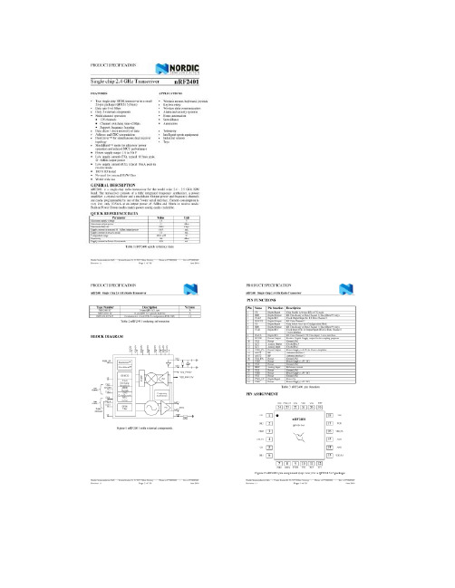
2.4GHz射频收发芯片nRF2401及其应用

2.4GHz射频收发芯片nRF2401及其应用2.4GHz射频收发芯片nRF2401及其应用2.4GHz射频收发芯片nRF2401及其应用2007-01-20电子通信论文2.4GHz射频收发芯片nRF2401及其应用摘要:本文介绍了工作于2.4GHzISM频段的射频收发芯片nRF2401的芯片结构、引脚功能、工作模式、接收与发送的工作流程,详细描述了nRF2401的器件配置,给出了应用电路图,分析了PCB设计时应该注意的问题,最后对全文进行了总结。
关键词:nRF2401;射频;无线通信;收发芯片 1.引言 nRF2401是单片射频收发芯片,工作于2.4~2.5GHzISM频段,芯片内置频率合成器、功率放大器、晶体振荡器和调制器等功能模块,输出功率和通信频道可通过程序进行配置。
芯片能耗非常低,以-5dBm的功率发射时,工作电流只有10.5mA,接收时工作电流只有18mA,多种低功率工作模式,节能设计更方便。
其DuoCeiverTM技术使nRF2401可以使用同一天线,同时接收两个不同频道的数据。
nRF2401适用于多种无线通信的场合,如无线数据传输系统、无线鼠标、遥控开锁、遥控玩具等。
2.芯片结构、引脚说明 2.1芯片结构 nRF2401内置地址解码器、先入先出堆栈区、解调处理器、时钟处理器、GFSK滤波器、低噪声放大器、频率合成器,功率放大器等功能模块,需要很少的外围元件,因此使用起来非常方便。
QFN24引脚封装,外形尺寸只有5×5mm。
nRF2401的功能模块如图1所示。
2.2引脚说明表1:nRF2401引脚3.工作模式 nRF2401有工作模式有四种:收发模式、配置模式、空闲模式和关机模式。
nRF2401的工作模式由PWR_UP、CE、TX_EN 和CS三个引脚决定,详见表2。
表2:nRF2401工作模式 3.1收发模式nRF2401的收发模式有ShockBurstTM收发模式和直接收发模式两种,收发模式由器件配置字决定,具体配置将在器件配置部分详细介绍。
- 1、下载文档前请自行甄别文档内容的完整性,平台不提供额外的编辑、内容补充、找答案等附加服务。
- 2、"仅部分预览"的文档,不可在线预览部分如存在完整性等问题,可反馈申请退款(可完整预览的文档不适用该条件!)。
- 3、如文档侵犯您的权益,请联系客服反馈,我们会尽快为您处理(人工客服工作时间:9:00-18:30)。
Range Extension for Nordic nRF24LE1 with RFaxis RFX2401C Single-Chip RFeIC™Test Summary, Technical Notesand Application SchematicBy Mike Atia and Najva Akbari, RFaxis Inc.September 2012ContentsContents (2)Figures (2)1.Introduction (3)2.RFX2401C Architecture (3)3.Experimental Setup (4)4.Receiver Sensitivity Improvement with RFX2401C (5)5.Boosting Transmitter Output Power with RFX2401C (5)6.Range Extension (7)7. Application Schematic and settings (8)8. FCC Compliance Testing (9)9. Conclusion (10)FiguresFigure 1: RFaxis RFX2401C RFeIC TM Block Diagram (3)Figure 2: Setup 1 with two NRF24LE1 (4)Figure 3: Setup 2 with RFX2401C at the TX side (4)Figure 4: Setup 3 with RFX2401C at the RX side (4)Figure 5: Setup 4 with RFX2401C at both ends (4)Figure 6: Effect of Receiver LNA on link extension (5)Figure 7: Measured output power with and without RFX2401C (6)Figure 8: RFX2401C current consumption as a function of total output power (6)Figure 9: Effect of Transmitter PA on link extension (7)Figure 10: Typical connection schematic between NRF24LE1 and RFX2401C (8)Figure 11: Spurious Response of the nRF24LE1 and RFX2401C (9)Figure 12: Harmonic Response of the nRF24LE1 and RFX2401C (10)1.IntroductionThe Nordic nRF24LE1 is an ultra-low power RF system on-chip (SoC) operating in the 2.4GHz ISM (Industrial, Scientific and Medical) band. It is a popular solution for a wide range of applications including wireless mouse, remote control, asset tracking, monitoring, medical sensor, home automation, and gaming. The maximum transmitted output power of the nRF24LE1 is +0dBm. The receiver Noise Figure is ~8dB. The nRF24LE1 is mainly used for short range application. Typical solution to extend the range involves adding a power amplifier to increase the transmitted power and a switch to change from transmitter to receiver path. This can increase and complicate the BOM. As shown in section 2, the RFaxis RFX2401C contain an LNA for the receiver, PA for the transmitter and two switches all in a single die. Adding the RFaxis RFX2401C RF Front-End IC (RFeIC™) can increase the transmitted power and reduce the receiver Noise Figure leading to range extension and more robust communication. This document summarizes the benefits of adding the RFX2401C to a transmitter receiver pair of nRF24LE1.Section 2 gives a brief overview of the architecture of the RFX2401C. Section 3 describes the different setups used to collect experimental results. Section 4 highlights improvements in the range by adding the RFX2401C at the receiver side. Section 5 contains improvements in the transmitter power together with the extra current used by the RFX2401C as a function of the output power. Section 6 contains the experimental results of the transmitter receiver pair. It also emphasizes the resulting range extension. Section 7 summarizes the implementation schematic of the connection between nRF24LE1 and RFX2401C. Section 8 summarizes the results of FCC Compliance testing of the setup.2.RFX2401C ArchitectureFigure 1: RFaxis RFX2401C RFeIC™ Block DiagramThe RFX2401C is a fully integrated, single-chip, single-die RFeIC (RF Front-end Integrated Circuit) which incorporates all the RF functionality needed for IEEE 802.15.4/ZigBee, wireless sensor network, and any other wireless systems in the 2.4GHz ISM band. The RFX2401C architecture integrates the PA, LNA, Transmit and Receive switching circuitry, the associated matching network, and the harmonic filter all in a CMOS single-chip device.3.Experimental SetupFor this experiment, the nRF24LE1 transceiver is used. In order to measure the effect of the RFX2401C on the transceiver, four setups are tested. The setups are shown in Figure 2, Figure 3, Figure 4, and Figure 5.Figure 2: Setup 1 with two nRF24LE1Figure 3: Setup 2 with one RFX2401C at the TX sideFigure 4: Setup 3 with an RFX2401C at the RX sideFigure 5: Setup 4 with RFX2401C at both endsThe experiment consists of the following steps:-Setting up a transmitter and receiver pair-The transmitter sends 100 packets of data to the receiver. Data rate of each packet is 2 Mbit -Attenuating the link until the number of received packets is 99%The nRF24LE1 transmitter has 4 different output power settings varying from -18dBm to 0dBm.4.Receiver Sensitivity Improvement with RFX2401CTo quantify the effect of the RFX2401C on the nRF24LE1 receiver, results from Setup 1 (Figure 2) and Setup 3 (Figure 4) are compared. The results are shown in Figure 6. For 99% of the received packets, the range difference between Setup 1 and Setup 3 is about 6dB. The plots show that adding the RFX2401C at the receiver side improves the link budget by 5~6dB. The range improvement results from the difference in noise figure of the RFX2401C LNA and nRF24LE1 LNA and also the gain of the RFX2401C LNA. The RFX2401C LNA draws about 10mA of current.Figure 6: Effect of Receiver LNA on link extension5.Boosting Transmitter Output Power with RFX2401CAs shown in section 2, the RFX2401C has both LNA and PA. When the nRF24LE1 output power is set to -18dBm, the gain of RFX2401C PA increases the transmitted antenna power by up to 24dB. At 0dBm output power setting of nRF24LE1, the maximum output power of the RFX2401C PA is 21dBm. Figure 7 shows the measured output power out of the nRF24LE1 standalone and with the RFX2401C. The corresponding RFX2401C current consumption as a function of output power is shown in Figure 8.Figure 7: Measured output power with and without RFX2401CFigure 8: RFX2401C current consumption as a function of total output powerThe corresponding attenuation results are shown in Figure 9. Adding the RFX2401C only to the transmitter improves the link by 6~24 dB. This large variation exists because the communication is bi-directional and using the RFX2401C only at one side does not amplify the transmit and receive signals by the same amount. In this setup, at higher power levels (0dBm in this case) the range can only be extended until the Acknowledge signal dies down because it is only amplified by the RFX2401C LNA. This limitation, however, does not exist when RFX2401C is used at both the receiver and the transmitter. This will be apparent in the next section.6.Range ExtensionAdding the RFX2401C at both ends of the link increases the range by 26~35dB. The maximum output power of the RFX2401C PA is about21dBm. At 0dBm nRF24LE1 output power setting, the range extension is about 26 dB. This is resulting from the RFX2401C PA increased output power of ~21dB and ~5dB from the RFX2401C receiver noise figure along with increased LNA gain.The effective distance improvement is calculated as , where ATTEN is the extra gain in dB. At 0dBm output power of NRF24LE1, RFX2401C improves the range by 26dB which is equivalent to about 20 times distance improvement. This range extension is based on the assumption that there is direct line of sight between the transmitter and the receiver. If there is any obstruction between the transmitter and the receiver, range will be different.7.Application Schematic and settingsThe schematic in Figure 12 shows the typical connections between the nRF24LE1 and RFX2401C. The setup is as follows:-TXRX port (Pin 4) of RFX2401C is connected to the ANT1 and ANT2 port of nRF24LE1 (Pin assignment depends on the packaging)-RXEN (Pin 6) of RFX2401C is connected to GPIO-TXEN (Pin 5) is connected to VDD_PA of nRF24LE1.The GPIO connected to RXEN must be programmed accordingly. Optional harmonic filter can be added at the antenna pin if the application is required to pass FCC. The schematic (Figure 10) shows that the required BOM is simple.Figure 10: Typical connection schematic between nRF24LE1 and8.FCC Compliance TestingRegulatory compliance testing is an important part of any product development effort, and is best addressed in the earliest stages of engineering. In order to provide an easy path to certification for future customers of this design configuration, an FCC pre-scan was performed on the reference design noted in Error! Reference source not found.. Not every required test was performed during this scan, but a thorough overall evaluation was given to the design especially to the tests that are typically the most difficult to pass. This includes the spurious emissions and the harmonics, which can be especially difficult in an RF transmitting system with a power amplifier.Figure shows the actual spurious response of the design as depicted in Error! Reference source not found.. As can be seen, the emissions are well below the limit line, which shows the design would easily pass this part of the test. It is worth noting that these emissions are typically not a function of the power amplifier design, but are usually due to other high speed digital and analog systems in the design. Careful design practices should always be followed to assure a compliant final product.Figure 11: Spurious Response of the nRF24LE1 and RFX2401CHarmonic testing is a very important aspect of FCC compliance which is directly related to the power amplifier design and operation. The hard limit for harmonics of the transmitted signal under FCC Part 15.247 at 3 meters is 74 dBuV peak, and 54 dBuV average. The table in Figure 1 of the measured results shows a compliance margin of greater than 3 dB on the average and 11 dB on the peak. These results were obtained with the output power set at +20dBm, which indicates this design is compliant when including the harmonic filter on the RFX2401C output.Figure 1: Harmonic Response of the nRF24LE1 and RFX2401C9. ConclusionAdding the RFX2401C at the receiver side improves the link by ~5dB. This is resulting from the gain of the RFX2401C LNA and delta in noise figure between the nRF24LE1 and the RFX2401C LNA. Adding RFX2401C to the transmit side will increase the output power of the setup to 21dBm. The overall range extension is achieved by connecting the RFX2401C at both ends of the link. At the 0dBm output power setting of nRF24LE1, the RFX2401C gives 26dB improvement in total link budget - which is equivalent to about 20 times improvement in LOS distance.。