SSD1305-Revision 2.0
戴尔Latitude 5540 用户手册

Latitude 5540用户手册4 2023注意、小心和警告:“注意”表示可帮助您更好地使用产品的重要信息。
:“小心”表示可能会导致硬件损坏或数据丢失,并告诉您如何避免问题。
:“警告”表示可能会导致财产损坏、人身伤害甚至死亡。
© 2023 Dell Inc. 或其子公司。
保留所有权利Dell Technologies、Dell 和其他商标均是 Dell Inc. 或其子公司的商标。
其他商标可能是其各自所有者的商标。
章 1: Latitude 5540的视图 (8)右 (8)左侧 (9)顶部 (10)正面 (11)背面 (12)底部 (12)服务编号 (12)电池电量和状态指示灯 (13)章 2: 设置 Latitude 5540 (14)章 3: Latitude 5540 的规格 (16)尺寸和重量 (16)处理器 (16)芯片组 (17)操作系统 (18)内存 (18)外部端口 (19)内部插槽 (19)以太网 (19)无线模块 (20)WWAN 模块 (20)音频 (21)存储 (22)介质卡读卡器 (22)键盘 (22)键盘功能键 (23)摄像头 (24)触控板 (24)电源适配器 (25)电池 (26)显示屏 (27)指纹读取器(可选) (28)传感器 (28)GPU —集成 (29)GPU —独立 (29)外部显示屏支持 (29)硬件安全性 (29)智能卡读卡器 (30)非接触式智能卡读卡器 (30)接触式智能卡读卡器 (31)操作和存储环境 (32)戴尔支持政策 (32)目录3Dell Optimizer 戴尔智能调优软件 (33)章 4: 拆装计算机内部组件 (34)安全说明 (34)拆装计算机内部组件之前 (34)安全防范措施 (35)静电放电— ESD 保护 (35)ESD 现场服务工具包 (36)运输敏感组件 (36)拆装计算机内部组件之后 (36)BitLocker (37)建议工具 (37)螺钉列表 (37)Latitude 5540的主要组件 (38)章 5: 卸下和安装客户可更换部件 (CRU) (41)SIM 卡托盘(可选) (41)卸下 SIM 卡托盘(可选) (41)安装 SIM 卡托盘(可选) (42)基座护盖 (43)卸下底座护盖 (43)安装底座护盖 (45)无线网卡 (48)卸下 WLAN 卡 (48)安装 WLAN 卡 (49)WWAN 卡(可选) (50)卸下 4G WWAN 卡(可选) (50)安装 4G WWAN 卡(可选) (51)卸下 5G WWAN 卡(可选) (53)安装 5G WWAN 卡(可选) (54)内存模块 (55)卸下内存模块 (55)安装内存模块 (56)固态驱动器 (57)卸下插槽 1 中的 M.2 2230 固态硬盘 (57)在插槽 1 中安装 M.2 2230 固态硬盘 (58)卸下插槽 1 中的 M.2 2280 固态硬盘 (59)在插槽 1 中安装 M.2 2280 固态硬盘 (60)卸下插槽 2 中的 M.2 2230 固态硬盘 (61)在插槽 2 中安装 M.2 2230 固态硬盘 (62)风扇 (63)卸下风扇 (63)安装风扇 (63)章 6: 卸下和安装现场可更换部件 (FRU) (65)电池 (65)锂离子电池预防措施 (65)4目录组件内框架 (69)卸下组件内框架 (69)安装组件内框架 (70)扬声器 (72)卸下扬声器 (72)安装扬声器 (73)币形电池 (74)卸下钮扣电池 (74)安装钮扣电池 (75)散热器 (76)卸下散热器(独立 GPU) (76)安装散热器(独立 GPU) (77)卸下散热器(集成 GPU) (78)安装散热器(集成 GPU) (79)系统板 (80)卸下系统主板 (80)安装系统主板 (83)电源按钮 (86)卸下电源按钮 (86)安装电源按钮 (87)电源按钮,带可选的指纹读取器 (88)卸下带可选指纹读取器的电源按钮 (88)安装带可选指纹读取器的电源按钮 (89)键盘 (90)卸下键盘 (90)安装键盘 (92)显示屏部件 (94)卸下显示屏组件 (94)安装显示屏组件 (97)显示屏挡板 (99)卸下显示屏挡板 (99)安装显示屏挡板 (99)显示屏面板 (100)卸下显示屏面板 (100)安装显示屏面板 (103)摄像头模块 (106)卸下摄像头模块 (106)安装摄像头模块 (107)显示屏转轴 (108)卸下显示屏转轴 (108)安装显示屏转轴 (109)显示屏后盖 (110)卸下显示屏后盖 (110)安装显示屏后盖 (111)显示屏线缆 (112)卸下显示屏线缆 (112)安装显示屏线缆 (113)传感器板 (114)目录5指纹读取器(可选) (116)卸下指纹读取器(可选) (116)安装指纹读取器(可选) (117)智能卡读卡器 (119)卸下智能卡读卡器 (119)安装智能卡读卡器 (119)虚拟 SIM 卡插槽填充挡片 (120)卸下虚拟 SIM 卡插槽填充挡片 (120)安装虚拟 SIM 卡插槽填充挡片 (121)掌托部件 (122)卸下掌托组件 (122)安装掌托组件 (124)章 7: 软件 (126)操作系统 (126)驱动程序与下载 (126)章 8: BIOS 设置 (127)进入 BIOS 设置程序 (127)导航键 (127)一次性启动菜单 (127)系统设置选项 (128)更新 BIOS (138)在 Windows 中更新 BIOS (138)在 Linux 和 Ubuntu 环境中更新 BIOS (138)在 Windows 环境中使用 USB 驱动器更新 BIOS (138)从 F12 一次性启动菜单更新 BIOS (139)系统密码和设置密码 (139)分配系统设置密码 (140)删除或更改现有的系统设置密码 (140)清除 CMOS 设置 (141)清除 BIOS(系统设置)和系统密码 (141)章 9: 故障排除 (142)处理膨胀锂离子电池 (142)找到戴尔计算机的服务编号或快速服务代码 (142)Dell SupportAssist 启动前系统性能检查诊断程序 (142)运行 SupportAssist 启动前系统性能检查 (143)内置自检 (BIST) (143)M-BIST (143)液晶屏电源导轨测试 (L-BIST) (143)液晶屏内置自检 (BIST) (144)系统诊断指示灯 (144)恢复操作系统 (145)实时时钟 (RTC) 重置 (145)备份介质和恢复选项 (146)Wi-Fi 重启 (146)6目录耗尽剩余弱电(执行硬重置) (146)章 10: 获取帮助和联系戴尔 (147)目录7Latitude 5540的视图右1.microSD 卡插槽针对 microSD 卡进行读取和写入。
Gen3i
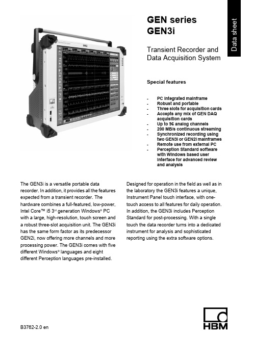
GEN series GEN3iTransient Recorder and Data Acquisition System Special features-PC integrated mainframe-Robust and portable-Three slots for acquisition cards -Accepts any mix of GEN DAQ acquisition cards-Up to 96 analog channels-200 MB/s continuous streaming -Synchronized recording using two GEN3i or GEN2i mainframes -Remote use from external PC -Perception Standard software with Windows based userinterface for advanced reviewand analysisThe GEN3i is a versatile portable data recorder. In addition, it provides all the features expected from a transient recorder. The hardware combines a full-featured, low-power, Intel Core™ i5 3rd generation Windows® PC with a large, high-resolution, touch screen and a robust three-slot acquisition unit. The GEN3i has the same form factor as its predecessor GEN2i, now offering more channels and more processing power. The GEN3i comes with five different Windows® languages and eight different Perception languages pre-installed.Designed for operation in the field as well as inthe laboratory the GEN3i features a unique, Instrument Panel touch interface, with one-touch access to all features for daily operation.In addition, the GEN3i includes PerceptionStandard for post-processing. With a singletouch the data recorder turns into a dedicated instrument for analysis and sophisticatedreporting using the extra software options.DatasheetB3762-2.0 enGEN3i Block DiagramFigure 1.1: Block Diagram GEN3i Portable RecorderWindows® PCMemory8 GB; DDR3 RAMProcessor Intel 3610ME, Core™ i5 3rd generation; 2 Core, 4 threads; 2.7 GHz, 3.3 GHz turbo Ethernet 3 * RJ45 Ethernet connection; 1 Gbit/s1 * RJ45 Ethernet connection with IEEE588 (PTP) support; 1 Gbit/s1 * SFP based optical Ethernet connection with IEEE588 (PTP) support; 1 Gbit/s; supports850 and 1310 nm SFP modules.Wake on LAN Supported on all Ethernet portsWireless LAN Embedded 801.11b/g/n; 54, 100 and 300 Mbit/s; Wireless LAN can be hardware disabled USB connectors USB 2.0, 2 on back + 2 on frontUSB 3.0, 4 on back (Using selective SSD > 100 MB/s continuous streaming)Internal storage PC disk Solid State Drive (SSD), unformatted size 480 GB, 200 MB/s continuous streaming Display TFT SXGA touch screen, 17” / 1280x1024 resolutionVideo connection 2 * Display port and 1 * DVI-D connector; CRT 2048 x 1536 and DVI-D 1600 x 1200 Multiple monitors support3; clone mode and extended modeSpeaker/Speaker Out Internal speaker/jack plug 3.5 mmMicrophone Jack plug 3.5 mmAccessories USB Keyboard and USB optical mouseFront panel controls4; Direct recording control Start/Stop/Pause/TriggerSoftwareInstrument panel / Touch interface (Fully touch-optimized)Setup of instrument, Acquisition control, Display data: live / review, Basic measurements, Export and archiving, Basic reportingDAQ software Perception Standard package. Refer to Perception specification sheet for details.DAQ software options Analysis, Advanced Report, Video Playback, Multi Workbooks, Information, Basic FFT,Sensor Database and moreDAQ Software and Instrument panel languages English, German, French, Chinese, Japanese, Korean, Russian, Portuguese (Brazilian) Operating system Microsoft Windows® 7 UltimateOperating system installed languages English, German, French, Chinese, JapaneseOther languages can be downloaded and installed using "Windows® Update"HBM2B3762-2.0 enApplication Programmers Interfaces (API)PNRF reader (free of charge)Functions Read PNRF, NRF and LRF recording files directly in your own applicationCOM interface The PNRF reader comes as COM interface and can be used from any application orprogramming language which supports COM automationPNRF Software Development Kit (SDK)Installs PNRF dll’s and supplies Visual Basic, C# and C++ getting started examples Matlab® integration Matlab® PNRF reader install and example available within the PNRF SDKLabVIEW™ integration Available directly from National InstrumentsDCE/RPC (Distributed Computing Environment/Remote Procedure Calls)Functions Control Perception software from an external computer/application on Windows®, Linux,Unix, Mac OS XCOM interface All RPC commands have a COM wrapper for easier Windows® software integration Available basic commands Load and Save Perception setup files, Setup Recording, set and review Hardware Settings,Start/Stop/Pause/Trigger, monitor Live dataExamples (free of charge)C++ and C# getting started example programs supplied for Windows®, source codeincluded. Unsupported Linux getting started example on request only.LabVIEW™ integration (free of charge)LabVIEW™ getting started example using RPC/COM availableCSI (Customer Software Interface)Functions Create software extension inside the Perception software by adding CSI user sheets,custom automation and extended analysis functions. Basic Windows C# sheet templateincluded. Available for all Microsoft .NET® 4 supporting languages.Available basic controls & commands Access to every Perception part: Start/Stop/Pause and Trigger, Start Manager, AcquisitionSystem, Hardware Settings, Displays, Meters, User Tables, Formulas, Calculations, DataManager, Data Sources, User variables, Notifications, Logging, Conversion Functions,Automation Actions, Sheet Manager and more, to create a dedicated application GUI thathides the entire Perception standard GUIExamples (free of charge)C# getting started example programs supplied, source code includedTraining/Support ProgramHBM offers paid professional training and support programs on all API interfaces (PNRF reader, RPC and CSI). Training program will be C# based, on-site or at central HBM location. On-site training can be customer specific. Support can be the development of a full custom software application or answering questions of software engineers.Acquisition SystemSystem Timebase and synchronizationCentral timebase for all acquisition cardsAccuracy± 3.5 ppm; aging after 10 years ± 10 ppmBase Binary, Decimal or ExternalSynchronization sources IEEE1588:2008 (PTP V2: Precision Time Protocol; using 2 step master protocol)Master/Slave synchronization; Slave or single Master modeMultiple Master mode scheduled for Q3 2014IRIG and GPS scheduled for Q3 2014PTP synchronization accuracy Synchronization accuracy reduces as network traffic increases on Ethernet port used forPTP synchronization± 150 ns; < 10% load no Ethernet switch used± 500 ns; < 50% load no Ethernet switch used± 5 μs; < 80% load no Ethernet switch usedTo avoid excessive network traffic blocking the PTP synchronization, separate thecommunication and PTP synchronization on two independent networks.Use 2 step master PTP aware switches to obtain best results across switches. Actualaccuracy depends on switch used. The use of switches without PTP support will create anunpredictable accuracy.Acquisition SlotsUnused slots must be covered using the GEN DAQ blank panel. This closes the mainframe front panels for EMC/EMI and safety compliance but also regulates the internal airflow for correct cooling of the acquisition system.Maximum slots3Acquisition boards All slots support any combination of GEN DAQ Acquisition boardsDigital Event/Timer/Counter connector1; Connected to slot A and BB3762-2.0 en3HBMAcquisition SystemThermal control Every acquisition board and the acquisition system monitors its own temperatures andstatus. This is used to regulate fan speeds and reduce noise while optimizing airflow andpower consumption.Calibration Any changes to the acquisition system configuration may change its internal thermalgradients. As accurate calibration relies on a steady and repeatable thermal environment,calibration will be void if changes are made in the configuration. See the individual cardspecifications for calibration impact.GEN3i Connection OverviewFigure 1.2: GEN3i Connection OverviewHBM4B3762-2.0 enMaster/Slave SynchronizationMainframe to mainframe phase shift± 100 nsLED signaling Optical link synchronized, not connected, function disabledMaster mode Basic and extended synchronization supported; 1 Slave maximum. Multiple slave supportedby Multi Slave option (Available Q3 2014)Slave mode Basic and extended synchronization supportedBasic synchronizationFirst sample Synchronizes the first sample in the recording for each mainframeSynchronized timebase Prevents frequency drift of the sample rates within each mainframeChannel trigger exchange Synchronously exchanges every channel trigger connected to the Master/Slave trigger busto/from each connected mainframeExtended synchronizationMaximum number of mainframes 2 (Can be used in mix with GEN2i, GEN3i and GEN3t mainframes)Synchronous recording actions Start/Stop and Pause of a recording across multiple mainframes each controlled by aseparate Perception. Stop recording is a non synchronous actionSynchronous manual trigger User action within Perception to trigger all mainframes synchronouslyCompatibility Basic synchronization features are backward compatible with GEN Series Master/Slavecard option for both Master and Slave modes. Extended synchronization features are notsupported by the Master/Slave card option. When using a mixed setup the system willautomatically work with basic synchronization onlyProbe CalibrationPins2; Signal and groundSignal~1 kHz square waveSignal amplitude0 V to 2 V using 1 MΩ load0 V to 1 V using 50 Ω loadB3762-2.0 en5HBMFigure 1.3: Pin assignment I/O ConnectorConnector type Tyco: 2-5747706-0 (D-sub, 9 pin female)Mating connector type Tyco: 5-747904-5Breakout cable (included)Cable type CoaxConnector type6; BNC femaleLength0.5 m (1.6 feet)External Timebase In TTL compatible, Low -30 V to 0.7 V, High 2 V to 30 VPulse width100 ns min.Maximum frequency 5 MHzActive edge RisingRounding resolution 4.01 µs; 250 kS/s and 20 kS/s acquisition cards1.01 µs; 1 MS/s and 200 kS/s acquisition cards510 ns; 2 MS/s and 200 kS/s (GN611) acquisition cards60 ns; 100 MS/s and 25 MS/s acquisition cardsInput to sample moment delay350 – 400 ns, plus maximum 1 full "rounding resolution"Input overvoltage protection± 30 V DCExternal Trigger In TTL compatible, Low -30 V to 0.7 V, High 2 V to 30 VResolution50 nsMinimum pulse width500 nsActive edge Selectable rising or fallingInput overvoltage protection± 30 V DCDelay(1)± 1 μs + maximum 1 sample period (for decimal and binary time base)Send to External Trigger Out User can select to forward External Trigger In to the External Trigger Out BNC Top Dead Center Rotational input Used to indicate top dead center in rotational external timebaseExternal Trigger Out TTL compatible; 0 V < Low < 0.6 V; 2 V < High < 5 VActive level Selectable High/Low/Hold HighPulse width High or Low selected: 12.8 µsHold High selected : Active from first trigger to end of recordingOutput impedance49.9 Ω ± 1 %Short circuit protected ContinuousDelay(1)516 ± 1 μs + maximum 1 sample period when Clock base: decimal, Filter: wideband(2)504 ± 1 μs + maximum 1 sample period when Clock base: binary, Filter: wideband(2)(1)Delays are equal for all acquisition cards.(2)If analog and/or digital filter is used extra delay will be added depending on type of filter and signal frequency.HBM6B3762-2.0 enExternal Event Out TTL compatible; 0 V < Low < 0.6 V; 2 V < High < 5 VFunction Selectable Alarm or Recording Active outputActive level Selectable High/Low for Alarm outputRecording active High outputPulse width Alarm: Active from start of alarm condition until condition endsRecording: Active until recording stopsOutput impedance49.9 Ω ± 1 %Short circuit protected ContinuousDelay(1)515 ± 1 μs + maximum 1 sample period when Clock base: decimal, Filter: wideband(2)503 ± 1 μs + maximum 1 sample period when Clock base: binary, Filter: wideband(2) External Start In TTL compatible, Low -30 V to 0.7 V, High 2 V to 30 VMinimum Pulse width200 nsActive edge Rising/falling edge; software selectableStart response time Typically 1 s when system is completely idleInput overvoltage protection± 30 V DCExternal Stop In TTL compatible, Low -30 V to 0.7 V, High 2 V to 30 VMinimum Pulse width200 nsActive edge Rising/falling edge; software selectableStop response time Typically 1 s when system is recording without automationInput overvoltage protection± 30 V DC(1)Delays are equal for all acquisition cards.(2)If analog and/or digital filter is used extra delay will be added depending on type of filter and signal frequency.Digital Event/Timer/CounterFigure 1.4: Digital Event/Timer/Counter block diagramSupported Cards See specifications of acquisition cardsNumber of Connectors1Connector Type44 pin, female D-type connector, AMP HD-22 series (Tyco: 5748482-5)Cable Connector Type44 pin, male D-type connector, HDP-22 series (Tyco: 1658680-1)Output PowerVoltage 5 ± 0.5 V DCMaximum current0.5 AEvent InputsNumber of events16 per card, 2 cards per connectorLevels TTL Compatible, Low -30 V to 0.7 V, High 2 V to 30 VB3762-2.0 en7HBMDigital Event/Timer/CounterFigure 1.5: Logic threshold voltage levelsOvervoltage protection± 30 V DCTimer/CounterNumber of channels Two per card, two cards per connectorFunctions See specifications of acquisition cards that support these inputsOutputsNumber of outputs Two per card, two cards per connectorFunctions See specifications of acquisition cards that support these outputsOutput levels TTL compatible; 0 V < Low < 0.6V; 2 V < High < 5 VOutput resistance49.9 Ω ± 1 %Output current20 mA, short circuit protectedDigital Event/Timer/Counter Connector Pin AssignmentFigure 1.6: Pin diagram for Digital Event/Timer/Counter connectorQuantumX Power SupplyConnector type ODU, G81L0C-P08LFG0-0000Mating connector type ODU, SX1LOC−P08MFG0−0000Connector pinning Only GND and PWR signal connectedOutput Power15 WattOutput Voltage> 11 V; Typical 11.5 V to 12 VMaximum Output Current 1.4 A; Current limited and short circuit protectedHBM8B3762-2.0 enPowerPower Inlet47-63 Hz, 100-240 V ACTotal Power of unit (maximum)250 VA, 300 VA peakPhysical, Weight and DimensionsWeightMainframe9 kg (20.9 lbs), add ≈ 1 kg (2.2 lbs) per acquisition board installedDimensionsHeight/Height with handle34.2 cm/39.2 cm (13.5"/15.4")Width43.6 cm (17.2")Depth18.6 cm (7.3")Acoustic Noise The total A-weighted SPL 55 dBA @ 0.6 m maximumTemperature Sensors Temperature for monitoring and air flow controlCooling Fans2Handle One carrying handle, also used for higher tilt anglesTilting Feet Two retractable feet for small tilt anglesGrounding 4 mm Banana plugCasing Aluminum/Plastic coverAccessories Soft carry case with strap for transportation included with hardened front and back forprotection, and storage pouches for mouse and keyboardFigure 1.7: GEN3i DimensionsB3762-2.0 en9HBMEnvironmental SpecificationsTemperature RangeOperational0 °C to +40 °C (+32 °F to +104 °F)Non-operational (Storage)-25 °C to +70 °C (-13 °F to +158 °F)Thermal protection Automatic thermal shutdown at 85 °C (+185 °F) internal temperatureUser warning notifications at 75 °C (+167 °F)Relative humidity0 % to 80 %; non-condensing; operationalProtection class IP20Altitude Maximum 2000 m (6562 feet); operationalShock: IEC 60068-2-27Operational Half-sine 10 g/11 ms; 3-axis, 1000 shocks in positive and negative directionNon-operational Half-sine 25 g/6 ms; 3-axis, 3 shocks in positive and negative direction Vibration: IEC 60068-2-34Operational 1 g RMS, ½ h; 3-axis, random 5 to 500 HzNon-operational 2 g RMS, 1 h; 3-axis, random 5 to 500 HzOperational Environmental TestsCold test IEC60068-2-1 Test Ad-5 °C (+23 °F) for 2 hoursDry heat test IEC-60068-2-2 Test Bd+40 °C (+104 °F) for 2 hoursDamp heat test IEC60068-2-3 Test Ca+40 °C (+104 °F), humidity >93 % RH for 4 daysNon-Operational (Storage) Environmental TestsCold test IEC-60068-2-1 Test Ab-25 °C (-13 °F) for 72 hoursDry heat test IEC-60068-2-2 Test Bb+70 °C (+158 °F) humidity <50 % RH for 96 hoursChange of temperature test IEC60068-2-14 Test Na -25 °C to +70 °C (-13 °F to +158 °F)5 cycles, rate 2 to 3 minutes, dwell time 3 hoursDamp heat cyclic test IEC60068-2-30 Test Db variant 1+25 °C/+40 °C (+77 °F/+104 °F), humidity >95/90 % RH 6 Cycles, cycle duration 24 hoursHarmonized Standards for CE Compliance, according to the following directivesLow voltage directive (LVD): 2006/95/ECElectromagnetic compatibility directive (EMC): 2004/108/ECElectrical SafetyEN 61010-1 (2010)Safety requirements for electrical equipment for measurement, control, and laboratory use - General requirements EN 61010-2-030 (2010)Particular requirements for testing and measuring circuitsElectromagnetic CompatibilityEN 61326-1 (2006)Electrical equipment for measurement, control and laboratory use - EMC requirements - Part 1: General requirements EMISSIONEN 55011Industrial, scientific and medical equipment - Radio-frequency disturbance characteristics - Limits and methods of measurementConducted disturbance: class B; Radiated disturbance: class AEN 61000-3-2Limits for harmonic current emissions: class DEN 61000-3-3Limitation of voltage changes, voltage fluctuations and flicker in public low-voltage supply systemsIMMUNITYEN 61000-4-2Electrostatic discharge immunity test (ESD);contact discharge ± 4 kV/air discharge ± 8 kV: performance criteria BEN 61000-4-3Radiated, radio-frequency, electromagnetic field immunity test;80 to 2700 MHz using 10 V/m, 1000 Hz AM: performance criteria AEN 61000-4-4Electrical fast transient/burst immunity testMains ± 2 kV using coupling network. Channel ± 2 kV using capacitive clamp: performance criteria BEN 61000-4-5Surge immunity testMains ± 0.5 kV/± 1 kV Line-Line and ± 0.5 kV/± 1 kV/± 2 kV Line-earth Channel ± 0.5 kV/± 1 kV using couplingnetwork: performance criteria BEN 61000-4-6Immunity to conducted disturbances, induced by radio-frequency fields0.15 to 80 MHz, 1000 Hz AM; 10 V RMS @ mains, 3 V RMS @ channel, both using clamp: performance criteria A EN 61000-4-11Voltage dips, short interruptions and voltage variations immunity testsDips: performance criteria A; Interruptions: performance criteria CHBM10B3762-2.0 enIRIG, IRIG/GPS (options, to be ordered separately; available Q2 2014)IRIG(1)Supported by IRIG and IRG/GPS optionTime Code Translator (Input)Time Code formats IRIG A and IRIG B, IEEE 1344 compliantAM Modulated or DC level shift (DCLS)Modulation ratio3:1 to 6:1Input amplitude500 mV to 5 V Peak-to-PeakInput impedance>10 kΩTime Code OutputTime Code format IRIG B, IEEE 1344 compliantModulation ratio3:1Output amplitude 4 V Peak-to-Peak (fixed) into 50 ΩDC level shift TTL/CMOSAM modulated input/output connectors 2 SMB sockets; one for input and one for outputDCLS connector Micro DP, 15-pin; some signals internally linked to Interface/Controller ModuleTime synchronization accuracy<5 µs modulated, <1 µs (DCLS)GEN DAQ series functions Capture start of recording timeSynchronize Master Time Base oscillator frequencyTime required to full synchronization after IRIG signal detectedNo recording active 1 to 5 minutesRecording or pause active 1 to 5 minutes plus 25 s per ms recording time deviation from IRIG timeUser notifications while recording Time marks on IRIG signal lost/restored and IRIG time synchronizedShort term tracking stability 5.0 E-8Long term tracking “Fly-wheeling” 5.0 E-7GPS(1)Only supported by IRG/GPS optionGPS connector Micro DP, 9-pinGPS antenna1; includedGPS antenna cable50 m (164 feet); includedTime synchronization accuracy<1 µsGEN DAQ series functions Capture start of recording timeSynchronize Master Time Base oscillator frequencyGPS localization time 2 to 15 minutesTime required to full synchronization after GPS localization completedNo recording active 1 to 10 minutesRecording or pause active 1 to 10 minutes plus 25 s per ms recording time deviation from IRIG timeUser notifications while recording Time marks on GPS satellites lost/restored and GPS time synchronizedShort term tracking stability 5.0 E-8Long term tracking “Fly-wheeling” 5.0 E-7(1)Requires factory installationMultiple Slave Card (option, available Q3 2014)In Master mode enables the synchronization of 2 or more Slaves. Single Slave control and Slave mode supported by mainframe Synchronization connector. Specifications to be determinedB3762-2.0 en11HBMShipping Case (option, to be ordered separately)Figure 1.8: Hardcover reusable shipment case with wheels and transport handleOutside Dimensions60.0 cm (23.6") x 32.5 cm (12.8") x 67.5 cm (26.5") (H x W x D)Weight Empty Case16.5 kg (36.3 lbs)System Storage Area Special area for system, slides in from the top for easy storage and removal from theshipment case. Protects the system for impact during drop, shock and vibrations Accessories Area Separate area for keyboard, mouse, power cable and some cablesReliable Case Transport Wheels and extendable handle constructed for stable transportation with low gravitationpoint to avoid tumbling of case in any direction during roll transportCase Extras Two lift handles and locks on side of the case for easy transportShock and Vibration Tested with system inside case according to ASTM D4728 EDrop Test Tested with system inside case according to ASTM D4169-04 Level IRack Mount Kit (option, to be ordered separately)Figure 1.9: GEN3i Rack Mount KitRack Mount Kit Mounting GEN3i mainframe in a standard 19” rack. Does not support the mouse andkeyboard delivered with the GEN3i. Requires no additional mounting materials. Userinstalled option.HBM12B3762-2.0 enFigure 1.10: Txx adapter block diagramTxx ConnectionNumber of Txx Torque transducers2Torque interface support Torque and ShuntSpeed interface support RPM and DirectionTxx signalsLevels Differential RS422Termination100 ΩB3762-2.0 en13HBMConnectorsGEN series interface HD22 sub-D 44 pin male (connecting cable included)Loop through event input44 pin, female D-type connector, AMP HD-22 series (Tyco: 5748482-5)Torque interface15 pin, female sub-D type (matches 1-KAB149-6)Speed/RPM interface15pin, female sub-D type (matches 1-KAB163-6)CablesTxx adapter to GEN2i/GEN3i/GEN3t0.5 m (1.64 Feet), included with Txx adapterTxx adapter to Txx Torque1-KAB149-6 (other lengths available), to be ordered separatelyTxx adapter to Txx Speed/RPM1-KAB163-6 (other lengths available), to be ordered separatelyPowerAdapter Power by GEN2i/GEN3i/GEN3tTxx Torque transducers Requires separate power supplyOutside dimensions 2.15 (54.60”) x 171.6 (6.76”) x 123.6 (4.86) (H x W x D)Figure 1.11: Txx adapter dimensionsHBM14B3762-2.0 enAcquisition CardsModel Type Isolation Max. SR(1)Resolution Memory(2)Channels Event, T/C(3) Basic200k Single Ended no200 kS/s16 bit128 MB80, 0Basic200k XT ISO Unbalanced Differential yes200 kS/s16 bit128 MB80, 0Basic1M Single Ended no 1 MS/s16 bit256 MB80, 0Basic1M ISO Unbalanced Differential yes 1 MS/s16 bit512 MB80, 0Basic1M XT ISO Unbalanced Differential yes 1 MS/s16 bit512 MB80, 0Bridge200k ISO Bridge/Differential yes200 kS/s16 bit128 MB40, 0Bridge1M ISO Bridge/Differential yes 1 MS/s16 bit512 MB40, 0Uni200k ISO Differential/IEPE/Shunt yes200 kS/s16 bit128 MB40, 0Uni1M ISO Differential/IEPE/Shunt yes 1 MS/s16 bit512 MB40, 0Basic20k-16Differential no20 kS/s16 bit200 MB1616, 0Basic20k-32Differential no20 kS/s16 bit200 MB3216, 0HiRes250k-16Differential/IEPE/Charge no250 kS/s16/24 bit1800 MB1616, 2HiRes250k-32Differential/IEPE/Charge no250 kS/s16/24 bit1800 MB3216, 2HiSpeed 25M Differential/Single Ended no25 MS/s15 bit128 MB40, 0HiSpeed 100M Differential/Single Ended no100 MS/s14 bit1800 MB40, 0Fiber100M 6600Optical Fiber yes100 MS/s--(4)1800 MB4(4)0, 0Fiber100M 7600Optical Fiber yes100 MS/s--(4)1800 MB4(4)0, 0Iso1kV200k Balanced Differential yes200 kS/s16/18 bit200 MB616, 2Iso1kV2M Balanced Differential yes 2 MS/s16/18 bit1800 MB616, 2Marker1M Binary no 1 MS/s 1 bit512 MB640, 0Marker1M HV Optical/Binary yes & no 1 MS/s 1 bit512 MB8 & 320, 0(1)Maximum Sample Rate/channel (not multiplexed).(2)Total recording memory/card.(3)Digital Events, Timer/Counter channels (Supported by GEN3i and GEN2i Digital Event/Timer/Counter connector only).(4)This card supports maximum four optical fiber transmitter channels.Optical Fiber Transmitter ChannelsTransmitterEvery transmitter is a single channel unit. Every unit has an unbalanced differential input, amplifier, analog anti alias filter and ADC with an optical data and control link to the receiver card. The receiver card has the recording logic, sample rate selection and memory.Model Receiver Card Power Sample rate Resolution IsolationHV6600 100M Fiber100M 6600Battery100 MS/s14 bit User application definedHV6600 25M Fiber100M 6600Battery25 MS/s15 bit User application definedMV6600 100M Fiber100M 6600120/240 V AC100 MS/s14 bit1800 V RMSMV6600 25M Fiber100M 6600120/240 V AC25 MS/s15 bit1800 V RMS7600 100M Fiber100M 7600External 12 V DC100 MS/s14 bit User application definedSpecial Function Cards5B Carrier Uses one GEN DAQ slot, holds up to six 5B modules. 5B modules, I/O connectors andcabling not included. An acquisition card is required for actual recording.The 5B Series signal conditioning modules provide a low cost method of connecting analogsignals with data acquisition systems. They are designed to convert thermocouples, RTD's,strain gages, frequencies, potentiometers, slide wires and other signals into standardized,isolated analog outputs.B3762-2.0 en15HBMOrdering Information (1)ArticleDescriptionOrder No.GEN3iGEN3i rugged, portable data recorder.(2)Integrated Instrument, with three acquisitions slots, 200 MB/s streaming rate, one Master/Slave connector, integrated PC, Windows ® 7 Ultimate,64 bit version. 17 inch touch screen TFT,480 GB Solid State Disk, Mouse, Keyboard,carrying bag with integrated protective front cover. Includes Perception Standard software package.1-GEN3i-2GEN3i plus one Iso1kV200k cardGEN3i - 6 channel Iso1kV200k package.Same as GEN3i plus one 1-GN611-2; 6 channel,1 kV isolated balanced differential inputs,200 kS/s, 128 MB RAM cards.1-GEN3i6-2GEN3i plus two Iso1kV200k cardsGEN3i - 12 channel Iso1kV200k package.Same as GEN3i plus two 1-GN611-2; 6 channel,1 kV isolated balanced differential inputs,200 kS/s, 128 MB RAM cards. (12 channels total).1-GEN3i12-2GEN3i plus three Iso1kV200k cardsGEN3i - 18 channel Iso1kV200k package.Same as GEN3i plus three 1-GN611-2; 6channel, 1 kV isolated balanced differential inputs, 200 kS/s, 128 MB RAM cards. (18channels total).1-GEN3i18-2(1)All GEN series systems are intended for exclusive professional and industrial use.(2)GEN3i ships with keyboard layout in English, German, French, Chinese or Japanese. Specify on order.HBM 16B3762-2.0 en。
国科环宇OpenVPX产品手册2014版

76
OV8301 3U 图像视频后 IO 板
78
OV8302 3U 标准配置后 IO 板
80
OpenVPX产品简介
OpenVPX是新一代高性能、高可靠计算机标准,国科环宇作为VITA组织会员之一, 秉承满足客户需求的理念,持续自主研发针对航空、航天、车载、舰载等恶劣环 境应用的OpenVPX标准高可靠计算机系列产品。国科环宇提供从整机到主机板、 功能板、接口板和背板等各种部件,以及全面的软件支持和技术服务。
AD接口板
OV4311 3U 四通道2.5Gsps
AD接口板
电源板
OV4312 3U QSFP接口板
后IO板
OV6301 3U 7槽0.85"背板
OV5300 3U K7 FPGA载板
OV5301 3U ProASIC3L FPGA载板
OV5311 3U XMC/PMC载板
OV7301 3U 180W电源板
整机
机箱
OV9370
OV9310Байду номын сангаас
OV93T0
OV96T0
OV96T1
3U 7槽导冷高可靠计算机 高可靠嵌入式GPU计算机 3U 7槽风冷调试平台 6U 8槽风冷上架平台 6U 5槽风冷上架平台
主机板
OV1300
OV1301
OV1302
3U 7槽1.0"导冷机箱 3U 7槽0.85"导冷机箱 3U 4槽 0.85"导冷机箱
OV8300 3U 管理控制后IO板
OV8301 3U 图像视频后IO板
OV8302 3U 标准配置后IO板
1
环境适应性等级
散热方式
LEVEL 0
MEMORY存储芯片DS1302N+中文规格书
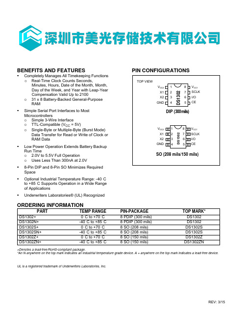
BENEFITS AND FEATURES▪Completely Manages All Timekeeping Functions o Real-Time Clock Counts Seconds,Minutes, Hours, Date of the Month, Month,Day of the Week, and Year with Leap-Year Compensation Valid Up to 2100o 31 x 8 Battery-Backed General-PurposeRAM ▪Simple Serial Port Interfaces to Most Microcontrollerso Simple 3-Wire Interface o TTL-Compatible (V CC = 5V)o Single-Byte or Multiple-Byte (Burst Mode)Data Transfer for Read or Write of Clock or RAM Data ▪Low Power Operation Extends Battery Backup Run Timeo 2.0V to 5.5V Full Operation o Uses Less Than 300nA at 2.0V ▪8-Pin DIP and 8-Pin SO Minimizes Required Space▪Optional Industrial Temperature Range: -40°C to +85°C Supports Operation in a Wide Range of Applications▪Underwriters Laboratories® (UL) RecognizedPIN CONFIGURATIONSORDERING INFORMATIONPARTTEMP RANGE PIN-PACKAGE TOP MARK* DS1302+ 0°C to +70°C 8 PDIP (300 mils) DS1302 DS1302N+ -40°C to +85°C 8 PDIP (300 mils) DS1302 DS1302S+ 0°C to +70°C 8 SO (208 mils) DS1302S DS1302SN+ -40°C to +85°C 8 SO (208 mils) DS1302S DS1302Z+ 0°C to +70°C 8 SO (150 mils) DS1302Z DS1302ZN+-40°C to +85°C8 SO (150 mils)DS1302ZN+Denotes a lead-free/RoHS-compliant package.*An N anywhere on the top mark indicates an industrial temperature grade device. A + anywhere on the top mark indicates a lead-free device.UL is a registered trademark of Underwriters Laboratories, Inc.REV: 3/15DETAILED DESCRIPTIONThe DS1302 trickle-charge timekeeping chip contains a real-time clock/calendar and 31 bytes of static RAM. It communicates with a microprocessor via a simple serial interface. The real-time clock/calendar provides seconds, minutes, hours, day, date, month, and year information. The end of the month date is automatically adjusted for months with fewer than 31 days, including corrections for leap year. The clock operates in either the 24-hour or 12-hour format with an AM/PM indicator.Interfacing the DS1302 with a microprocessor is simplified by using synchronous serial communication. Only three wires are required to communicate with the clock/RAM: CE, I/O (data line), and SCLK (serial clock). Data can be transferred to and from the clock/RAM 1 byte at a time or in a burst of up to 31 bytes. The DS1302 is designed to operate on very low power and retain data and clock information on less than 1µW.The DS1302 is the successor to the DS1202. In addition to the basic timekeeping functions of the DS1202, the DS1302 has the additional features of dual power pins for primary and backup power supplies, programmable trickle charger for V CC1, and seven additional bytes of scratchpad memory.OPERATIONFigure 1 shows the main elements of the serial timekeeper: shift register, control logic, oscillator, real-time clock, and RAM.Figure 1. Block DiagramTYPICAL OPERATING CHARACTERISTICS (V CC = 3.3V, T A = +25°C, unless otherwise noted.)OSCILLATOR CIRCUITThe DS1302 uses an external 32.768kHz crystal. The oscillator circuit does not require any external resistors or capacitors to operate. Table 1 specifies several crystal parameters for the external crystal. Figure 1 shows a functional schematic of the oscillator circuit. If using a crystal with the specified characteristics, the startup time is usually less than one second.CLOCK ACCURACYThe accuracy of the clock is dependent upon the accuracy of the crystal and the accuracy of the match between the capacitive load of the oscillator circuit and the capacitive load for which the crystal was trimmed. Additional error will be added by crystal frequency drift caused by temperature shifts. External circuit noise coupled into the oscillator circuit may result in the clock running fast. Figure 2 shows a typical PC board layout for isolating the crystal and oscillator from noise. Refer to Application Note 58: Crystal Considerations for Dallas Real-Time Clocks for detailed information.Table 1. Crystal Specifications*PARAMETER SYMBOL MIN TYP MAX UNITSNominal Frequency f O32.768 kHzSeries Resistance ESR 45 kΩLoad Capacitance C L 6 pF*The crystal, traces, and crystal input pins should be isolated from RF generating signals. Refer toApplication Note 58: Crystal Considerations for Dallas Real-Time Clocks for additional specifications.COMMAND BYTEFigure 3 shows the command byte. A command byte initiates each data transfer. The MSB (bit 7) must be a logic 1.If it is 0, writes to the DS1302 will be disabled. Bit 6 specifies clock/calendar data if logic 0 or RAM data if logic 1. Bits 1 to 5 specify the designated registers to be input or output, and the LSB (bit 0) specifies a write operation (input) if logic 0 or read operation (output) if logic 1. The command byte is always input starting with the LSB (bit 0). Figure 3. Address/Command Byte。
HPE ProLiant DL380 Gen9 服务器用户指南
©Copyright 2014, 2016 Hewlett Packard Enterprise Development LP 本文档中包含的信息如有更改,恕不另行通知。
随 Hewlett Packard Enterprise 产品和服务提供的明确保修声明中阐明了此类产品和服务的全部保修服务。
本文档中的任何内容均不应理解为构成任何额外保证。
Hewlett Packard Enterprise 对本文档中出现的技术错误、编辑错误或遗漏之处概不负责。
指向第三方网站的链接将访问 Hewlett Packard Enterprise 网站以外的位置。
Hewlett Packard Enterprise 无法控制 Hewlett Packard Enterprise 网站以外的信息,也不承担任何责任。
Microsoft® 和 Windows® 是 Microsoft Corporation 在美国和/或其它国家(地区)的注册商标或商标。
Linux® 是 Linus Torvalds 在美国和其它国家/地区的注册商标。
Red Hat® 是 Red Hat, Inc. 在美国和其它国家/地区的注册商标。
Java 是 Oracle 和/或其分支机构的注册商标。
SD 和 microSD 是 SD-3C 在美国和/或其它国家/地区的商标或注册商标。
VMware 是 VMware, Inc. 在美国和/或其它司法辖区的注册商标或商标。
Intel® 和 Xeon® 是 Intel Corporation 在美国和其它国家/地区的商标。
部件号:768830-AA52016 年 3 月版本:5目录1 组件识别 (1)前面板组件 (1)前面板 LED 指示灯和按钮 (2)UID 按钮功能 (5)电源故障 LED 指示灯 (5)访问可选的 HPE Systems Insight 显示屏 (5)Systems Insight 显示屏 LED 指示灯 (6)Systems Insight 显示屏 LED 指示灯组合 (7)后面板组件 (9)后面板 LED 指示灯 (10)Flex 插槽备用电池模块 LED 指示灯和按钮 (10)非热插拔 PCI Riser 卡插槽定义 (11)主板组件 (13)系统维护开关 (14)NMI 功能 (15)DIMM 插槽位置 (15)SAS 和 SATA 设备编号 (15)热插拔驱动器 LED 定义 (19)NVMe SSD 组件 (20)热插拔风扇 (20)2 操作 (23)打开服务器电源 (23)关闭服务器电源 (23)将服务器从机架中拉出 (23)将服务器从机架中取出 (24)卸下检修面板 (24)安装检修面板 (25)接触产品后面板 (25)打开理线臂 (25)卸下风扇笼 (26)卸下热插拔风扇 (27)卸下 PCI Riser 卡笼 (28)安装 PCI Riser 卡笼 (29)ZHCN iii固定全长扩展卡固定器 (30)卸下隔气罩 (31)安装隔气罩 (32)3 设置 (34)可选服务 (34)最佳环境 (34)空间要求与通风要求 (34)温度要求 (35)电源要求 (35)电气接地要求 (35)将直流电源线连接到直流电源 (36)机架警告 (37)查看服务器包装箱中的物品 (37)安装硬件选件 (37)将服务器装入机架 (37)安装操作系统 (39)通电并在 UEFI 引导模式下选择引导选项 (39)开机并选择引导选项 (40)注册服务器 (40)4 硬件选件安装 (41)Hewlett Packard Enterprise 产品规格说明简介 (41)简介 (41)热插拔驱动器准则 (41)驱动器选件 (41)卸下硬盘驱动器空闲挡板 (41)安装热插拔 SAS 或 SATA 驱动器 (42)卸下热插拔 SAS 或 SATA 硬盘驱动器 (43)安装 NVMe 驱动器 (43)Express 托架驱动器笼 (44)安装通风标签 (45)安装 Express 托架驱动器笼 (46)冗余热插拔电源选件 (53)高性能风扇选件 (55)处理器和风扇选件 (56)内存选件 (61)内存-处理器兼容性信息 (61)iv ZHCNSmartMemory (63)内存子系统体系结构 (64)单列、双列和四列 DIMM (64)DIMM 标识 (64)内存配置 (65)高级 ECC 内存配置 (66)联机备用内存配置 (66)镜像内存配置 (66)一般 DIMM 插槽安装准则 (66)高级 ECC 安装准则 (67)联机备用安装准则 (68)安装顺序 (68)镜像内存安装准则 (68)识别处理器类型 (68)安装 DIMM (68)通用介质托架选件 (69)2 插槽 PCI Riser 卡笼选件 (72)3 插槽 PCI Riser 卡笼选件 (74)GPU 扩展套件 (76)用于托架 1 的 8 托架 SFF 前驱动器笼选件 (82)用于托架 2 的 8 托架 SFF 前驱动器笼选件 (86)3 托架 LFF 后驱动器笼选件 (90)2 托架 SFF 前驱动器笼选件 (95)2 托架 SFF 后驱动器笼选件 (100)Systems Insight 显示屏电源开关模块选件 (107)位置查找服务耳选件 (109)Smart Storage 电池 (112)FlexibleLOM 选件 (113)扩展卡选件 (115)卸下扩展插槽空闲挡板 (115)安装扩展卡 (116)HPE H240 Smart HBA/P440、P840 Flexible Smart Array 控制器 (117)HPE P440ar/P840ar Flexible Smart Array 控制器 (120)12G SAS 扩展卡 (122)后串行端口选件 (129)M.2 SSD 支持卡选件 (130)在 M.2 SSD 支持卡上安装 SSD 模块 (131)安装 M.2 SSD 支持卡 (132)ZHCN v双 8 Gb microSD 企业中级 USB 设备 (133)750 瓦 Flex 插槽热插拔备用电池模块 (134)Flex 插槽备用电池模块配置负载支持 (134)安装 FSBBU (134)HP Trusted Platform Module 选件 (136)安装 Trusted Platform Module 板卡 (137)保留恢复密钥/密码 (138)启用 Trusted Platform Module (139)5 布线 (140)2 托架 SFF 驱动器笼选件布线 (140)3 托架 LFF 后驱动器笼布线 (143)8 托架 SFF 前驱动器笼布线 (146)Express 托架支持选件布线 (151)主机总线适配器和控制器布线 (155)HPE H240 Smart 主机总线适配器/Smart Array P440 控制器布线 (155)HPE Smart Array P840 控制器布线 (158)HPE Smart Array P440ar 控制器布线 (160)HPE Smart Array P840ar 控制器布线 (164)通用介质托架布线 (168)150 瓦 PCIe 电源线选件 (172)M.2 SSD 支持卡选件布线 (172)6 软件和配置实用程序 (174)服务器模式 (174)产品 QuickSpecs (174)HPE iLO (175)Active Health System (175)适用于 iLO 的 RESTful API 支持 (176)Integrated Management Log (176)HPE Insight Remote Support (177)HPE Insight Remote Support 集中连接 (177)HPE Insight Online 直接连接 (177)Insight Online (177)Intelligent Provisioning (178)HPE Insight Diagnostics (178)HPE Insight Diagnostics 检测功能 (178)Erase Utility (179)适用于 Windows 和 Linux 的 Scripting Toolkit (179)vi ZHCNService Pack for ProLiant (179)HP Smart Update Manager (179)HPE UEFI System Utilities (180)使用 UEFI System Utilities (180)灵活的引导控制 (181)恢复和自定义配置设置 (181)安全引导配置 (181)嵌入的 UEFI Shell (182)嵌入式诊断选件 (182)适用于 UEFI 的 RESTful API 支持 (182)重新输入服务器序列号和产品 ID (182)实用程序和功能 (183)HPE Smart Storage Administrator (183)Automatic Server Recovery(自动服务器恢复) (183)USB 支持 (183)外置 USB 功能 (184)支持冗余 ROM (184)安全性和安全优势 (184)使系统保持最新状态 (184)获取 Hewlett Packard Enterprise 支持材料 (184)更新固件或系统 ROM (185)FWUPDATE 实用程序 (185)UEFI System Utilities 中的固件更新应用程序 (185)联机刷新组件 (186)驱动程序 (186)软件和固件 (186)支持的操作系统版本 (186)版本控制 (187)适用于 ProLiant 服务器的操作系统和虚拟化软件支持 (187)HPE 技术服务组合 (187)更改控制和主动通知 (187)7 故障排除 (188)故障排除资源 (188)8 更换电池 (189)ZHCN vii9 保修和管制信息 (191)保修信息 (191)管制信息 (191)安全和管制标准 (191)白俄罗斯、哈萨克斯坦、俄罗斯标志 (191)土耳其 RoHS 材料内容声明 (192)乌克兰 RoHS 材料内容声明 (192)10 规格 (193)环境规格 (193)机械规格 (193)电源规格 (194)HPE 500 瓦 Flex 插槽白金级热插拔电源 (195)HPE 800 瓦 Flex 插槽白金级热插拔电源 (196)HPE 800 瓦 Flex 插槽超钛金级热插拔电源 (196)HPE 800 瓦 Flex 插槽通用热插拔电源 (197)HPE 800 瓦 Flex 插槽 -48 伏(直流)热插拔电源 (198)HPE 1400 瓦 Flex 插槽超白金级热插拔电源 (199)HPE 750 瓦 Flex 插槽热插拔备用电池模块 (199)热插拔电源计算 (200)11 支持和其它资源 (201)访问 Hewlett Packard Enterprise 支持 (201)要收集的信息 (201)访问更新 (201)网站 (201)客户自行维修 (202)远程支持 (202)12 缩略语和缩写 (203)13 文档反馈 (207)索引 (208)viii ZHCN1组件识别前面板组件●SFF 型号(8 驱动器)编号说明1托架 1(可选驱动器或通用介质托架)2托架 2(可选驱动器)3固定的驱动器托架4前 USB 3.0 接口5序列号标签拉片●SFF 型号(24 驱动器)编号说明1托架 12托架 23托架 3,固定的驱动器托架ZHCN前面板组件1编号说明4前 USB 3.0 接口5序列号标签拉片●LFF 型号(12 驱动器)编号说明1-12驱动器托架●LFF 型号(4 驱动器)编号说明1-4驱动器托架前面板 LED 指示灯和按钮●SFF 前面板 LED 指示灯和按钮2第 1 章 组件识别ZHCN编号说明状态1开机/待机按钮和系统电源 LED 指示灯*绿色常亮 = 系统已启动绿色闪烁(1 赫兹/周每秒)= 正在执行开机过程琥珀色常亮 = 系统处于待机状态熄灭 = 未通电**2运行状况 LED 指示灯*绿色常亮 = 正常绿色闪烁(1 赫兹/周每秒)= iLO 正在重新引导琥珀色闪烁 = 系统性能下降红色闪烁(1 赫兹/周每秒)= 系统出现严重问题†3NIC 状态 LED 指示灯*绿色常亮 = 具有到网络的链路绿色闪烁(1 赫兹/周每秒)= 有网络活动熄灭 = 没有网络活动4UID 按钮/LED 指示灯*蓝色常亮 = 已激活蓝色闪烁:● 1 赫兹/周每秒 = 正在进行远程管理或固件升级● 4 赫兹/周每秒 = 已启动 iLO 手动重新引导过程●8 赫兹/周每秒 = 正在执行 iLO 手动重新引导过程ZHCN前面板 LED 指示灯和按钮3熄灭 = 已停用*当此表中所述的四个 LED 指示灯同时闪烁时,表示发生电源故障。
i3SOCV2.0产品规格书

文档来源为:从网络收集整理.word版本可编辑.欢迎下载支持.i3SOC V2.0产品规格书(方案用)神州数码索贝科技有限公司目录目录...................................................................... 错误!未定义书签。
1规格 ......................................................................... 错误!未定义书签。
1.1NVR系列 ........................................................................... 错误!未定义书签。
1.1.1i3NVR网络视频录像机............................................. 错误!未定义书签。
1.1.2i3NVR-LE/16网络视频录像机软件 ........................... 错误!未定义书签。
1.2CMS中心平台.................................................................... 错误!未定义书签。
1.2.1i3SMS6000安防管理服务器..................................... 错误!未定义书签。
1.2.2i³SPS6000安防平台服务器...................................... 错误!未定义书签。
1.2.3i3NVS网络视频服务器 ............................................. 错误!未定义书签。
1.3安防存储系统 .................................................................. 错误!未定义书签。
英飞凌低压MOS选型
Product Type BSB012NE2LX BSB014N04LX3 G BSB015N04NX3 G BSB017N03LX3 G BSB012N03LX3 G BSB028N06NN3 G BSB044N08NN3 G BSB056N10NN3 G BSB013NE2LXI BSB008NE2LX BSB150N15NZ3 G BSB280N15NZ3 G BSF024N03LT3 G BSF050N03LQ3 G BSF077N06NT3 G BSF030NE2LQ BSF134N10NJ3 G IPB067N08N3 G IPB023N04N G IPB034N03L G IPB015N04L G IPB027N10N3 G IPB035N08N3 G IPB015N04N G IPB019N06L3 G IPB083N10N3 G IPB042N10N3 G IPB054N06N3 G IPB034N06L3 G IPB039N04L G IPB037N06N3 G IPB041N04N G IPB048N06L G IPB050N06N G IPB097N08N3 G IPB052N04N G IPB055N03L G IPB054N08N3 G IPB042N03L G IPB022N04L G IPB065N03L G IPB072N15N3 G IPB049N06L3 G IPB025N08N3 G IPB080N03L G IPB081N06L3 G IPB075N04L G IPB114N03L G IPB093N04L G IPB147N03L G IPB096N03L G IPB136N08N3 G
IPB200N15N3 G IPB090N06N3 G IPB029N06N3 G IPB021N06N3 G IPB230N06L3 G IPB260N06N3 G IPB049NE7N3 G IPB031NE7N3 G IPB020NE7N3 G IPB123N10N3 G IPB038N12N3 G IPB144N12N3 G IPB320N20N3 G IPB107N20N3 G IPB200N25N3 G IPB600N25N3 G BUZ32 H3045A BUZ31 H3045A IPB108N15N3 G BUZ30A H3045A IPB065N15N3 G IPB530N15N3 G SPB100N03S2-03 G IPB009N03L G IPB011N04L G IPB011N04N G IPB016N06L3 G IPB017N06N3 G IPB019N08N3 G IPB020N04N G IPB023N06N3 G IPB025N10N3 G IPB030N08N3 G IPB039N10N3 G IPB036N12N3 G IPB034N06N3 G SPD07N20 G IPD031N06L3 G IPD034N06N3 G IPD035N06L3 G IPD036N04L G IPD038N06N3 G IPD038N04N G IPD048N06L3 G IPD053N06N3 G IPD053N08N3 G SPD50N03S2L-06 G SPD30N03S2L-07 G IPD068N10N3 G SPD50N03S2-07 G IPD079N06L3 G IPD082N10N3 G IPD088N04L G IPD088N06N3 G IPD096N08N3 G SPD30N03S2L-10 G
MicroDIMM设计规范
4.20.12 - 214-Pin DDR2 SDRAM Unbuffered MicroDIMM DesignSpecificationPC2-4200/PC2-3200 DDR2 Unbuffered MicroDIMM Reference Design SpecificationRevision 0.526,April, 2004Contents1. Product Description (3)Product Family Attributes (3)Raw Card Summary (3)2. Environmental Requirements (4)Absolute Maximum Ratings (4)3. Architecture (4)Pin Description (4)Input/Output Functional Description (5)DDR2 SDRAM MicroDIMM Pinout (6)Block Diagram x16 2Ranks Raw Card A (7)Block Diagram x16 1Rank Raw Card B (8)4. Component Details (9)x16 Ballout for 256Mb, 512Mb, 1Gb, 2Gb and 4Gb DDR2 SDRAMs (Top View) (9)DDR2 SDRAM FBGA Component Specifications (9)Reference SPD Component Specifications (9)SPD Component DC Electrical Characteristics (9)5. Unbuffered MicroDIMM Details (10)DDR2 SDRAM Module Configurations (Reference Designs) (10)Input Loading Matrix (10)DDR2 MicroDIMM Gerber File Releases (11)Example Raw Card Component Placement (12)6. MicroDIMM Wiring Details (13)Signal Groups (13)General Net Structure Routing Guidelines (13)Explanation of Net Structure Diagrams (13)Differential Clock Net Structures (14)Data Net Structures (16)Control Net Structures S[1:0], CKE[1:0], ODT[1:0] (18)Address/Control Net Structures Ax, BAx, RAS, CAS, WE (19)Cross Section Recommendations (21)Test Points (22)7. Serial Presence Detect Definition (23)Serial Presence Detect Data Example (23)8. Product Label (26)9. MicroDIMM Mechanical Specifications (27)1. Product DescriptionThis reference specification defines the electrical and mechanical requirements for the PC2-4200 memory module, a 214-pin, 267 MHz clock (533 MT/s data rate), 64-bit wide, Unbuffered Synchronous Double Data Rate 2(DDR2) DRAM Micro Dual In-Line Memory Module (DDR2 SDRAM MicroDIMMs). It also defines a slower version, the PC2-3200, using 200MHz clock (400 MT/s data rate) DDR2 SDRAMs. These DDR2 SDRAM MicroDIMMs are intended for use as main memory when installed in systems such as mobile per-sonal computers.Reference design examples are included which provide an initial basis for Unbuffered MicroDIMM designs. Any modifications to these reference designs must meet all system timing, signal integrity and thermal requirements for 267 MHz clock rate support. Other designs are acceptable, and all Unbuffered DDR2MicroDIMM implementations must use simulations and lab verification to ensure proper timing requirements and signal integrity in the design.Raw Card SummaryProduct Family AttributesAttribute:Values:Notes:MicroDIMM Organizationx 64MicroDIMM Dimensions (nominal)30 mm high, 54.0mm wide MicroDIMM Types Supported Unbuffered Pin Count214SDRAMs Supported 256 Mb, 512 Mb, 1 Gb, 2 Gb, 4 GbCapacity128 MB, 256 MB, 512 MB, 1 GB, 2GB, 4 GB Serial Presence DetectConsistent with JEDEC Rev. 1.0Voltage Options, Nominal1.8 V V DD 1.8 V V DD Q1.8 V to 3.3 V V DD SPD 1InterfaceSSTL_18Note 1: V DD SPD is not tied to V DD or V DD Q on the DDR2 MicroDIMM.Raw CardNumber of DDR2 SDRAMsSDRAM OrganizationNumber of RanksA 8x162B4x1612. Environmental RequirementsPC2-4200 DDR2 SDRAM Unbuffered MicroDIMMs are intended for use in mobile computing environments that have limited capacity for heat dissipation.3. ArchitectureAbsolute Maximum RatingsSymbol ParameterRating Units Notes T OPR Operating Temperature (ambient) 0 to +65°C 1H OPR Operating Humidity (relative) 10 to 90%1T STG Storage Temperature-50 to +100°C 1H STGStorage Humidity (without condensation) 5 to 95%1Barometric Pressure (operating & storage)105 to 69kPa1, 21.Stresses greater than those listed may cause permanent damage to the device. This is a stress rating only, and device functional operation at or above the conditions indicated is not implied. Exposure to absolute maximum rating conditions for extended periods may affect reliability.2.Up to 9850 ft.Pin DescriptionCK[1:0] Clock Inputs, positive line 2 DQ[63:0] Data Input/Output 64CK[1:0]Clock inputs, negative line 2DM[7:0] Data Masks 8CKE[1:0]Clock Enables 2DQS[7:0]Data strobes8RAS Row Address Strobe 1DQS[7:0]Data strobes complement8CAS Column Address Strobe 1WE Write Enable 1NC,TESTLogic Analyzer specific test pin (No connecton MicroDIMM1S[1:0]Chip Selects2A[9:0],A[15:11]Address Inputs15V DD Core and I/O Power 15A10/AP Address Input/Autoprecharge 1V SS Ground56BA[2:0] SDRAM Bank Address 3V REF Input/Output Reference 1ODT[1:0]On-die termination control2V DD SPD SPD Power1SCL Serial Presence Detect (SPD)Clock Input1RFU Reserved for future use 12 SDA SPD Data Input/Output 1 NCNo connect4SA[1:0]SPD address2Total:214Input/Output Functional DescriptionSymbol Type Polarity FunctionCK0/CK0, CK1/CK1InputCrosspointThe system clock inputs. All address and command lines are sampled on the cross point of therising edge of CK and falling edge of CK. A Delay Locked Loop (DLL) circuit is driven from theclock inputs and output timing for read operations is synchronized to the input clock.RFU pins for 2 CK pairs reserved.CKE[1:0]Input Active High Activates the DDR2 SDRAM CK signal when high and deactivates the CK signal when low. By deactivating the clocks, CKE low initiates the Power Down mode or the Self Refresh mode. RFU pins for 2 CKEs reserved.S[1:0]Input Active Low Enables the associated DDR2 SDRAM command decoder when low and disables the com-mand decoder when high. When the command decoder is disabled, new commands are ignored but previous operations continue. Rank 0 is selected by S0; Rank 1 is selected by S1. Ranks are also called "Physical banks". RFU pins for 2 Ss reserved.RAS, CAS,WE Input Active Low When sampled at the cross point of the rising edge of CK and falling edge of CK CAS, RAS, and WE define the operation to be executed by the SDRAM.BA[2:0]Input—Selects which DDR2 SDRAM internal bank of four or eight is activated.ODT[1:0]Input Active High Asserts on-die termination for DQ, DM, DQS, and DQS signals if enabled via the DDR2SDRAM mode register. RFU pins for 2 ODTs reserved.A[9:0],A10/AP, A[15:11]Input—During a Bank Activate command cycle, defines the row address when sampled at the crosspoint of the rising edge of CK and falling edge of CK. During a Read or Write command cycle,defines the column address when sampled at the cross point of the rising edge of CK and fall-ing edge of CK. In addition to the column address, AP is used to invoke autoprecharge opera-tion at the end of the burst read or write cycle. If AP is high, autoprecharge is selected andBA0-BAn defines the bank to be precharged. If AP is low, autoprecharge is disabled. During aPrecharge command cycle, AP is used in conjunction with BA0-BAn to control which bank(s) toprecharge. If AP is high, all banks will be precharged regardless of the state of BA0-BAninputs. If AP is low, then BA0-BAn are used to define which bank to precharge.DQ[63:0]In/Out—Data Input/Output pins.DM[7:0]Input Active High The data write masks, associated with one data byte. In Write mode, DM operates as a byte mask by allowing input data to be written if it is low but blocks the write operation if it is high. In Read mode, DM lines have no effect.DQS[7:0], DQS[7:0]In/Out CrosspointThe data strobes, associated with one data byte, sourced with data transfers. In Write mode,the data strobe is sourced by the controller and is centered in the data window. In Read mode,the data strobe is sourced by the DDR2 SDRAMs and is sent at the leading edge of the datawindow. DQS signals are complements, and timing is relative to the crosspoint of respectiveDQS and DQS. If the module is to be operated in single ended strobe mode, all DQS signalsmust be tied on the system board to VSS and DDR2 SDRAM mode registers programmedappropriately.V DD, V DD SPD,V SSSupply—Power supplies for core, I/O, Serial Presence Detect, and ground for the module.SDA In/Out—This is a bidirectional pin used to transfer data into or out of the SPD EEPROM. A resistor must be connected to V DD to act as a pull up.SCL Input—This signal is used to clock data into and out of the SPD EEPROM. A resistor may be con-nected from SCL to V DD to act as a pull up.SA[1:0]Input—Address pins used to select the Serial Presence Detect base address. RFU pins for 2nd SPD reserved.NC,TEST In/Out—The TEST pin is reserved for bus analysis tools and is not connected on normal memory mod-ules (MicroDIMMs)..DDR2 SDRAM MicroDIMM PinoutPin #LowerSidePin#UpperSidePin#LowerSidePin#UpperSidePin#LowerSidePin#UpperSidePin#LowerSidePin#UpperSide1V REF108V SS28DQS2135Vss55BA0162BA182DQ43189DQ47 2V SS109DQ429Vss136DQ2856WE163RAS83V SS190V SS 3DQ0110DQ530DQ18137DQ2957V DD164V DD84DQ48191DQ52 4DQ1111V SS31DQ19138Vss58RFU(S2)165S085DQ49192DQ535V SS112DM032Vss139DQS359RFU(ODT2)166ODT086V SS193V SS6DQS0113V SS33DQ24140DQS360CAS167A1387RFU(CK3)194CK17DQS0114DQ634DQ25141Vss61V DD168V DD88RFU(CK3)195CK18V SS115DQ735Vss142DQ3062S1169RFU(S3)89V SS196V SS9DQ2116V SS36DM3143DQ3163ODT1170RFU(ODT3)90DM6197DQS610DQ3117DQ1237Vss144Vss64V DD171V DD91V SS198DQS6 11V SS118DQ1338DQ26145NC,TEST65NC172NC92DQ50199V SS 12DQ8119V SS39DQ27146V DD66V SS173V SS93DQ51200DQ54 13DQ9120DM140Vss147CKE167DQ32174DQ3694V SS201DQ5514V SS121V SS41NC148RFU(CKE3)68DQ33175DQ3795DQ56202V SS15RFU(CK2)122CK042V DD149V DD69V SS176V SS96DQ57203DQ6016RFU(CK2)123CK043CKE0150A1570DQS4177DM497V SS204DQ6117V SS124V SS44RFU(CKE2)151A1471DQS4178V SS98DQS7205V SS18DQS1125DQ1445V DD152V DD72V SS179DQ3899DQS7206DM7 19DQS1126DQ1546BA2153A1273DQ34180DQ39100V SS207V SS 20V SS127V SS47A11154A974DQ35181V SS101DQ58208DQ62 21DQ10128DQ2048A7155A875V SS182DQ44102DQ59209DQ63 22DQ11129DQ2149V DD156V DD76DQ40183DQ45103V SS210V SS 23Vss130Vss50A5157A677DQ41184V SS104SDA211SA0 24DQ16131DM251A4158A378V SS185DQS5105SCL212RFU(*1) 25DQ17132Vss52A2159A179DM5186DQS5106NC213SA1 26Vss133DQ2253V DD160V DD80V SS187V SS107V DD SPD214RFU(*2) 27DQS2134DQ2354A10/AP161A081DQ42188DQ46Note: NC = No Connect; NC,TEST(pin 145) is for bus analysis tool and is not connected on normal memory modules. (*1) = SA0 for 2nd SPD, (*2) = SA1 for 2nd SPD.Block Diagram: Raw Card Version A (Populated as 2 ranks of x16 SDRAMs)Block Diagram: Raw Card Version B (Populated as 1 rank of x16 SDRAMs)#Unless otherwise noted, resistorand V DD Q values are 22 Ω ± 5%DQ wiring may differ from that described in this drawing;however, DQ/DM/DQS/DQS relationships are maintained as shown8pFLoad CapacitorsA0-AN RAS CAS WEmatching on ± 0.5pFBA0-BA23.0Ω±5%4. Component Detailsx16 Ballout for 256Mb, 512Mb, 1Gb, 2Gb and 4Gb DDR2 SDRAMs (Top View) 123789NC NC A NC NCBCVDD NC VSS D VSSQ UDQS VDDQ UDQ6VSSQ UDM E UDQS VSSQ UDQ7 VDDQ UDQ1VDDQ F VDDQ UDQ0VDDQ UDQ4VSSQ UDQ3G UDQ2VSSQ UDQ5VDD NC VSS H VSSQ LDQS VDDQ LDQ6VSSQ LDM J LDQS VSSQ LDQ7 VDDQ LDQ1VDDQ K VDDQ LDQ0VDDQ LDQ4VSSQ LDQ3L LDQ2VSSQ LDQ5 VDDL VREF VSS M VSSDL CK VDD CKE WE N RAS CK ODT BA2BA0BA1P CAS CSA10A1R A2A0VDD VSS A3A5T A6A4A7A9U A11A8VSS VDD A12A14V A15A13WYNC NC AA NC NCDDR2 SDRAM FBGA Component SpecificationsThe DDR2 SDRAM components used with this DIMM design specification are intended to be consistent with JEDEC MO-207 DK-Z and DL-Z.Reference SPD Component SpecificationsThe Serial Presence Detect EEPROMs have their own power pin, V DD SPD, so that they can be programmed or read without powering up the rest of the module. The wide voltage range permits use with 1.8V, 2.5V or 3.3V serial buses.SPD Component DC Electrical CharacteristicsSymbol Parameter Min Max UnitsV DD SPD Core Supply Voltage 1.7 3.6V5. Unbuffered MicroDIMM DetailsDDR2 SDRAM Module Configurations (Reference Designs)Raw Card MicroDIMMCapacityMicroDIMMOrganizationSDRAMDensitySDRAMOrganization# ofSDRAMs# ofRanksSDRAMPackage Type# of banks inSDRAM# Address bitsrow/colA256 MB32 M x 64256 Mbit16 M x 1682FBGA413/9 A512 MB64 M x 64512 Mbit32 M x 1682FBGA413/10 A 1 GB128 M x 64 1 Gbit64 M x 1682FBGA813/10 A 2 GB256 M x 64 2 Gbit128 M x 1682FBGA814/10 A 4 GB512 M x 64 4 Gbit256 M x 1682FBGA8TBDRaw Card MicroDIMMCapacityMicroDIMMOrganizationSDRAMDensitySDRAMOrganization# ofSDRAMs# ofRanksSDRAMPackage Type# of banks inSDRAM# Address bitsrow/colB128 MB16 M x 64256 Mbit16 M x 1641FBGA413/9 B256 MB32 M x 64512 Mbit32 M x 1641FBGA413/10 B512 MB64 M x 64 1 Gbit64 M x 1641FBGA813/10B 1 GB128 M x 64 2 Gbit128 M x 1641FBGA814/10B 2 GB256 M x 64 4 Gbit256 M x 1641FBGA8TBD Input Loading MatrixSignal NamesInputDeviceR/C A R/C BClock (CKn, CKn )SDRAM42 CKEn/Sn/ODTn SDRAM44 Addr/RAS/CAS/BA/WE SDRAM84 DQn/DQSn/DQSn/DMn SDRAM21 SCL/SDA/SAn EEPROM11DDR2 MicroDIMM Gerber File ReleasesReference design file updates will be released as needed. This specification will reflect the most recent design files, but may be updated to reflect clarifications to the specification only; in these cases, the design files will not be updated. The following table outlines the most recent design file releasesNote: Future design file releases will include both a date and a revision label. All changes to the design file are also documented within the ‘read-me’ file.Raw Card SpecificationRevisionApplicable Design File NotesA0.5A0 B0.5B0Example Raw Card Component PlacementThe component layout for Raw Cards A, and B are similar. In the case of Raw Card B, DDR2 SDRAMs will be included on the front side of the card; however, passive components are on both sides of the board. This example is for reference only; refer to JEDEC standard MO-TBD for details.6. MicroDIMM Wiring DetailsSignal GroupsThis specification categorizes SDRAM timing-critical signals into four groups whose members have identical loadings and routings. The following table summarizes the signals contained in each group..Signal Group Signals In Group PageClocks for Unbuffered MicroDIMM CK [1:0], CK [1:0]14, 15Data, Data Mask, Data Strobe DQ [63:0], DM[7:0], DQS[7:0], DQS[7:0]16, 17Select, Clock Enable, ODT S [1:0], CKE [1:0], ODT[1:0]18Address/Control Ax, BAx, RAS, CAS, WE19, 20General Net Structure Routing GuidelinesNet structures and lengths must satisfy signal quality and setup/hold time requirements for the memory inter-face. Net structure diagrams for each signal group are shown in the following sections. Each diagram is accompanied by a trace length table that lists the minimum and maximum allowable lengths for each trace segment and/or net.The general routing recommendations are as follows. Other stackups and layouts are possible that meet the electrical characteristics.•Route all signal traces using appropriate trace width(e.g: 0.075mm) and enough spacing(e.g: 0.15mm) between adjacent traces considering cross talk effect.•Route clocks as much as possible using the inner layers.•Test points are required.Explanation of Net Structure DiagramsThe net structure routing diagrams provide a reference design example for each raw card version. These designs provide an initial basis for unbuffered MicroDIMM designs. The diagrams should be used to deter-mine individual signal wiring on a MicroDIMM for any supported configuration. Only transmission lines (repre-sented as cylinders and labeled with trace length designators “TL”) represent physical trace segments. All other lines are zero in length. To verify MicroDIMM functionality, a full simulation of all signal integrity and tim-ing is required. The given net structures and trace lengths are not inclusive for all solutions.Once the net structure has been determined, the permitted trace lengths for the net structure can be read from the table below each net structure routing diagram. Some configurations require the use of multiple net structure routing diagrams to account for varying load quantities on the same signal. All diagrams define one load as one DDR2 SDRAM input unless mentioned. It is highly recommended that the net structure routing data in this document be simulated by the user.Differential Clock Net Structures CK[1:0], CK[1:0]DDR2 SDRAM clock signals must be carefully routed to meet the following requirements:•Signal quality •Rise/Fall time•Cross point of the differential pair in the SDRAM •JEDEC-compatible reference delays•Minimal segment length differences (less than 2.54mm total) between clocks of the same functionClock Net Wiring (Raw card A)Clock Routing Trace Lengths (Raw card A)Raw card TL0 Outer TL1 Inner TL2 Inner TL3 Outer TL4 Inner TL5 Outer Notes Min Max Min Max Min Max Min Max Min Max Min Max A2.02.36.26.77.78.13.84.36.37.90.70.911.All distances are given in millimeters and must be kept within a tolerance of ± 0.8 millimeter.TL0MicroDIMM ConnectorTL1TL2TL3TL3CK CKSDRAM SDRAMTL5TL2TL3TL3SDRAMSDRAMTL5R = 200 Ω± 5%R = 200 Ω± 5%TL4TL4Clock Net Wiring (Raw card B)Clock Routing Trace Lengths (Raw card B)Raw card TL0 Outer TL1 Inner TL2 Inner TL3 Outer TL4 Outer Notes Min Max Min Max Min Max Min Max Min Max B2.02.318.218.47.78.13.84.31.52.011.All distances are given in millimeters and must be kept within a tolerance of ± 0.8 millimeter.TL0MicroDIMM ConnectorTL1TL2TL3CK CKSDRAMTL2TL3SDRAMR = 200 Ω± 5%R = 200 Ω± 5%TL4TL4Data Net StructuresDQ[63:0], DM[7:0], DQS[7:0], DQS[7:0]Special attention has been paid to balancing the data nets within a DDR2 SDRAM, within a particularMicroDIMM, and across the MicroDIMM family. Data nets have been placed in order to bound the data strobe nets. Because data travels with the data strobe, the placement of the strobe in the middle of the narrow win-dow aids in data timing. Although it is not necessary to ensure consistent delays between SDRAMs and/or card types, doing so facilitates system design, system simulation, and DIMM specifications. It is recommend to maintain consistent delays for all nets as described in the following tables.Net Structure Routing for DQ[63:0], DM[7:0], DQS[7:0], DQS[7:0] (Raw card A)Trace Lengths for DQ[63:0], DM[7:0], DQS[7:0], DQS[7:0] (Raw card A)Raw card TL0 Outer TL1 Outer TL2 Outer TotalR1Ohms Notes Min Max Min Max Min Max Min Max A1.04.618.720.92.93.125.325.5221,2,3,41.All distances are given in millimeters and must be kept within a tolerance of ± 0.8 millimeter.2.Total Min and Total Max refer to the min and max respectively of TL0 + TL1 + TL2.3.TL0 and TL1 of Raw Card A is adjusted to compensate for the delay caused by vias on DQ nets. Traces with one via are assumed to have 1.6mm additional length. Traces with two vias are assumed to have 3.2mm additional length.4.These signals must be referenced to ground.TL0MicroDIMM Connector22 Ω ± 5%TL2SDRAM PinTL2SDRAM PinTL1Net Structures Routing for DQ[63:0], DM[7:0], DQS[7:0], DQS[7:0] (Raw card B )Trace Lengths for DQ[63:0], DM[7:0], DQS[7:0], DQS[7:0] (Raw card B )Raw cardTL0 Outer TL1 OuterTotalR1Ohms Notes Min Max Min Max Min Max B1.04.621.723.925.325.5221,2,3,41.All distances are given in millimeters and must be kept within a tolerance of ± 0.8 millimeter.2.Total Min and Total Max refer to the min and max respectively of TL0 + TL1.3.TL0 and TL1 of Raw Card B is adjusted to compensate for the delay caused by via on DQ nets.Traces with one via are assumed to have 1.6mm additional length. Traces with two vias are assumed to have 3.2mm additional length.4.These signals must be referenced to ground.TL0MicroDIMM Connector22 Ω ± 5%SDRAM PinTL1Control Net Structures S [1:0], CKE[1:0], ODT[1:0] (Raw cards A, B)Net Structure Routing for Control Net Structures S [1:0], CKE[1:0], ODT[1:0] (Raw cards A, B)Trace Lengths for Control Net Structures S [1:0], CKE[1:0], ODT[1:0] (Raw cards A, B)TL0 OuterTL1 Outer/Inner TL2 Inner TL3 Inner TL4 Outer Notes Raw CardMin Max Min Max Min Max Min Max Min Max A 1.0 4.622.029.116.017.5 6.57.1 2.7 4.21,2,3B1.04.622.029.116.017.56.57.12.74.21,2,31. All distances are given in mm and should be kept within a tolerance of ± 0.8 mm2. TL0 and TL1 are adjusted to compensate for the delay caused by via. Traces with one via are assumed to have 1.6mm additional length. Traces with two vias are assumed to have3.2mm additional length.3. These signals must be referenced to VDD.TL0MicroDIMM ConnectorTL2TL23.0 Ω ± 5%TL1TL3TL3TL4SDRAM PinTL4SDRAM PinTL4SDRAM PinTL3TL3TL4SDRAM PinAddress/Control Net Structures Ax, BAx, RAS, CAS, WE (Raw card A ).Net Structure Routing for Address/Control Net Structures Ax, BAx, RAS, CAS, WE (Raw card A )Trace Lengths for Address/Control Net Structures Ax, BAx, RAS, CAS, WE (Raw card A )TL0 OuterTL1 Outer/Inner TL2 Inner TL3 inner TL4 Outer Notes Raw CardMin Max Min Max Min Max Min Max Min Max A1.04.622.029.116.017.56.57.11.08.31,2,31. All distances are given in mm and should be kept within a tolerance of ± 0.8 mm2. TL0 and TL1 are adjusted to compensate for the delay caused by via. Traces with one via are assumed to have 1.6mm additional length. Traces with two vias are assumed to have3.2mm additional length. 3. These signals must be referenced to VDD.TL0MicroDIMM ConnectorTL4SDRAM PinTL2TL23.0 Ω ± 5%TL1TL3TL3TL4SDRAM PinTL4SDRAM PinTL4SDRAM PinTL4SDRAM PinTL3TL3TL4SDRAM Pin TL4SDRAM PinTL4SDRAM PinAddress/Control Net Structures Ax, BAx, RAS, CAS, WE (Raw card B).Net Structure Routing for Address/Control Net Structures Ax, BAx, RAS, CAS, WE (Raw card B)Trace Lengths for Address/Control Net Structures Ax, BAx, RAS, CAS, WE (Raw card B)TL0 OuterTL1 Outer/Inner TL2 Inner TL3 inner TL4 Outer TL5 Outer Notes Raw CardMin Max Min Max Min Max Min Max Min Max Min Max B1.04.622.029.116.017.56.57.11.08.33.04.01,2,31. All distances are given in mm and should be kept within a tolerance of ± 0.8 mm2. TL0 and TL1 are adjusted to compensate for the delay caused by via. Traces with one via are assumed to have 1.6mm additional length. Traces with two vias are assumed to have3.2mm additional length.3. These signals must be referenced to VDD.TL0MicroDIMM ConnectorTL2TL23.0 Ω ± 5% TL1TL3TL3TL4SDRAM PinTL4SDRAM PinTL4SDRAM PinTL3TL3TL4SDRAM PinTL58pF ± 0.5pFCross Section RecommendationsAn example of the DDR2 MicroDIMM printed circuit board design uses six-layers of glass epoxy material. PCBs should contain full plane layers for reference plane. The reference planes can be divided so adjacent signal layers maintain a constant Vss or Vdd reference. All data group signals are referenced to Vss and all address/command are referenced to Vdd. The required board impedance is 60 Ω± 10%.PCB Electrical SpecificationsParameter Min Max UnitsTrace velocity: S0 (outer layers) 5.5 6.7ps/mmTrace velocity: S0 (inner layers) 6.57.6ps/mmTrace impedance: Z0 (all layers)5466OhmsExample Layer Stackup for 0.075mm width traceTest PointsAll DDR2 components are in BGA packages which makes the package pads inaccessible for probing during-system development. The DDR2 MicroDIMMs have test points identified to make initial evaluation easier. In some cases test pads have been added and in other cases existing vias are used as test points. An effort has been made to provide testability on some signals in all signal groups but 100% coverage is not possible.Raw Card A Test Points Example(Front View)DQ22CK0-CK1-DQS at resistor pack.CK0CK1DQ7DQ44DQ52DQ28Raw Card B Test Points Example(Front View)BA2DQ22CK0-CK1-A7A3A12A10A9A14S0-A11A6BA0A2BA1CKE0A15A5A1CAS-ODT0RAS-WE-DQS at resistor pack.CK0CK1DQ7DQ44DQ52A13A0A4A8DQ28DQ367. Serial Presence Detect DefinitionThe Serial Presence Detect (SPD) function MUST be implemented on the PC2-4200 DDR2 SDRAM Unbuf-fered MicroDIMM. The component used and the data contents must adhere to the most recent version of the JEDEC DDR2 SDRAM SPD Specifications. Please refer to this document for all technical specifications and requirements of the serial presence detect devices.The following table is intended to be an example of a typical PC2-4200 MicroDIMM. SPD values indicating different MicroDIMM performance characteristics will be utilized based on specific characteristics of the SDRAMs or MicroDIMMs. This example assumes:•Module Organization: 512MB•Device Composition: 32Mx16•Device Package: FBGA•Module Physical Ranks: 2•CAS latency: 4(DDR2-533), 3(DDR2-400)Serial Presence Detect Data Example (Part 1 of 3)Byte # (dec)Byte #(hex)DescriptionSPD Entry ValueSerial PDData Entry(Hexadecimal)NotesDDR2-533DDR2-400DDR2-533DDR2-400000Number of Serial PD Bytes written during production128801 101Total Number of Bytes in Serial PD device256082202Fundamental Memory Type (FPM, EDO, SDRAM,DDR, DDR2, ...)DDR2 SDRAM08303Number of Row Addresses on Assembly130D 404Number of Column Addresses on Assembly100A505Number of DIMM RanksModule height:30mm, Planar,card on card: no,2Ranks61606Data Width of this Assembly x6440 707Reserved Undefined00 808Voltage Interface Level of this assembly SSTL 1.8V05909SDRAM Cycle Time at maximum supported CASlatency (CL), CL = X3.75ns 5.00ns3D503100A SDRAM Access from Clock+/-0.50ns+/-0.50ns5050110B DIMM configuration type (Non-parity, or ECC)Non-Parity00120C Refresh Rate/Type7.8us/SR823,4 130D Primary SDRAM Width x1610140E Error Checking SDRAM Width NA00150F Reserved Undefined001.This will typically be programmed as 128 bytes.2.This will typically be programmed as 256 bytes.3.From Data sheet.4.High order bit is self refresh "flag". If set to "1", the assembly supports self refresh.5.These are optional, in accordance with JEDEC specification.1610SDRAM device attributes: Burst lengths supported4,80C1711SDRAM device attributes: Number of Banks onSDRAM device40431812SDRAM device attributes: CAS Latency4310083 1913Reserved Undefined000 2014DIMM type information MicroDIMM082115SDRAM Module Attributes Normal DIMM002216SDRAM device attributes: General no optional aspect002317Minimum Clock Cycle at CLX -1Undefined FF32418Maximum Data Access Time (t AC) from Clock at CLX -1Undefined FF32519Minimum Clock Cycle Time at CLX-2Undefined FF3261A Maximum Data Access Time (t AC) from Clockat CLX-2Undefined FF3271B Minimum Row Precharge Time (t RP)15.0ns15.0ns3C3C3 281C Minimum Row Active to Row Active delay (t RRD)7.5ns7.5ns1E1E3 291D Minimum RAS to CAS delay (t RCD)15.0ns15.0ns3C3C3 301E Minimum Active to Precharge Time (t RAS)45.0ns45.0ns2D2D3 311F Module Rank Density256MB403220Address and Command input Setup Time BeforeClock (t IS)0.60ns0.60ns606033321Address and Command input Hold Time After Clock(t IH)0.60ns0.60ns606033422Data Input Setup Time Before Clock (t DS)0.35ns0.35ns35353 3523Data Input Hold Time After Clock (t DH)0.35ns0.35ns35353 3624Write recovery time (t WR)15.0ns15.0ns3C3C3 3725Internal write to read command delay (t WTR)7.5ns10ns1E283 3826Internal read to precharge command delay (t RTP)7.5ns7.5ns1E1E3 3927Memory analysis probe characteristics Undefined004028Reserved Undefined004129SDRAM device minimum active to active/auto refreshtime (t RC)60.0ns60.0ns3C3C3422A SDRAM device minimum auto-refresh to active/autorefresh command period (t RFC)105.0ns105.0ns69693Serial Presence Detect Data Example (Part 2 of 3)Byte # (dec)Byte #(hex)DescriptionSPD Entry ValueSerial PDData Entry(Hexadecimal)NotesDDR2-533DDR2-400DDR2-533DDR2-4001.This will typically be programmed as 128 bytes.2.This will typically be programmed as 256 bytes.3.From Data sheet.4.High order bit is self refresh "flag". If set to "1", the assembly supports self refresh.5.These are optional, in accordance with JEDEC specification.。
HP-DL380-Gen10-服务器用户手册 -
© Copyright 2017, 2018 Hewlett Packard Enterprise Development LP通知本文档中包含的信息如有更改,恕不另行通知。
随 Hewlett Packard Enterprise 产品和服务提供的明确保修声明中阐明了此类产品和服务的全部保修服务。
此处的任何内容都不应视作额外的担保信息。
对于本文档中包含的技术或编辑方面的错误或疏漏,Hewlett Packard Enterprise 不承担任何责任。
保密的计算机软件。
必须具有 Hewlett Packard Enterprise 颁发的有效许可证,方可拥有、使用或复制本软件。
按照 FAR 12.211 和 12.212 的规定,可以根据供应商的标准商业许可证授权美国政府使用商用计算机软件、计算机软件文档以及商业编号的技术数据。
单击指向第三方网站的链接将会离开 Hewlett Packard Enterprise 网站。
Hewlett Packard Enterprise 无法控制 Hewlett Packard Enterprise 网站之外的信息,也不对这些信息承担任何责任。
目录组件标识 (8)前面板组件 (8)前面板 LED 指示灯和按钮 (10)UID 按钮功能 (13)前面板 LED 指示灯电源故障代码 (13)Systems Insight 显示屏 LED 指示灯 (14)Systems Insight 显示屏组合 LED 指示灯说明 (15)后面板组件 (17)后面板 LED 指示灯 (17)主板组件 (19)系统维护开关说明 (20)DIMM 标签识别 (21)DIMM 插槽位置 (22)NVDIMM 识别 (22)NVDIMM 二维码 (23)识别 NVDIMM LED 指示灯 (24)NVDIMM-N LED 指示灯组合 (24)NVDIMM 功能 LED 指示灯运行模式 (24)处理器、散热片和插槽组件 (25)驱动器 (25)SAS/SATA 驱动器组件和 LED 指示灯 (26)NVMe SSD LED 指示灯定义 (26)uFF 驱动器组件和 LED 指示灯 (28)风扇托架编号 (29)驱动器盒识别 (29)驱动器托架编号 (31)驱动器托架编号:Smart Array 控制器 (31)驱动器托架编号:SAS 扩展卡 (33)驱动器托架编号:NVMe 驱动器 (35)uFF 驱动器托架编号 (36)转接卡组件 (37)带集成备用电池装置组件和 LED 指示灯的 HPE Flex 插槽电源 (41)检查备用电池电量 (41)HPE 12G SAS 扩展卡端口编号 (42)HPE Smart Array P824i-p MR Gen10 控制器 (42)操作 (44)打开服务器电源 (44)关闭服务器电源 (44)从机架中拉出服务器 (44)从机架中卸下服务器 (45)使用理线臂固定电缆 (45)卸下检修面板 (46)安装检修面板 (47)卸下风扇笼 (47)安装风扇笼 (48)卸下隔气罩或中板驱动器笼 (48)安装隔气罩 (50)卸下转接卡笼 (51)3卸下转接卡插槽空闲挡板 (52)卸下硬盘驱动器空闲挡板 (53)松开理线臂 (53)找到 Systems Insight 显示屏 (53)设置 (55)HPE 支持服务 (55)设置服务器 (55)运行要求 (58)空间要求与通风要求 (58)温度要求 (59)电源要求 (59)电气接地要求 (59)将直流电源线连接到直流电源 (59)服务器警告和注意事项 (60)机架警告 (61)静电释放 (61)服务器包装箱内物品 (62)安装硬件选件 (62)POST 屏幕选项 (62)安装或部署操作系统 (62)注册服务器 (62)硬件选件安装 (63)产品规格说明简介 (63)简介 (63)在安全挡板中安装风扇过滤器 (63)安装挡板和挡板锁 (64)电源供电选件 (64)热插拔电源计算 (64)安装冗余热插拔电源 (64)驱动器选件 (65)驱动器准则 (65)支持的驱动器托架 (66)安装热插拔 SAS 或 SATA 驱动器 (66)安装 NVMe 驱动器 (67)安装 uFF 驱动器和 SCM 驱动器托盘 (68)安装 M.2 驱动器 (69)风扇选件 (70)安装高性能风扇 (71)内存选件 (72)DIMM 和 NVDIMM 安装信息 (72)HPE SmartMemory 速度信息 (73)安装 DIMM (73)HPE 16GB NVDIMM 选件 (74)NVDIMM 支持的服务器要求 (74)安装 NVDIMM (74)为 NVDIMM 配置服务器 (76)NVDIMM 清理 (76)NVDIMM 移动准则 (77)HPE 可扩展持久性内存(仅限 CTO) (77)控制器选件 (78)安装存储控制器 (78)在配置的服务器中安装 HPE Smart Array P824i-p MR Gen10 控制器 (79)4阵列和控制器配置 (80)安装通用介质托架 (81)驱动器笼选件 (83)安装前 8NVMe SSD Express 托架驱动器笼 (83)安装前 6SFF SAS/SATA + 2NVMe Premium 驱动器笼 (85)安装通风标签 (87)在盒 1 中安装前 8SFF SAS/SATA 驱动器笼 (88)在盒 2 中安装前 8SFF SAS/SATA 驱动器笼 (90)安装前 2SFF NVMe/SAS/SATA Premium 驱动器笼 (92)安装中板 4LFF SAS/SATA 驱动器笼 (95)在主转接卡或辅助转接卡中安装后 2SFF SAS/SATA 驱动器笼 (98)在电源上方安装后 2SFF SAS/SATA 驱动器笼 (100)安装后 3LFF SAS/SATA 驱动器笼 (103)转接卡和转接卡笼选件 (104)安装主转接卡和辅助转接卡 (105)安装第三转接卡 (106)安装辅助转接卡笼 (107)安装第三转接卡笼 (108)安装 2NVMe slimSAS 转接卡选件 (111)安装 8NVMe slimSAS 转接卡选件 (112)扩展槽 (113)支持的 PCIe 外形尺寸 (113)安装扩展卡 (114)安装 12G SAS 扩展卡 (116)安装加速器或 GPU (118)安装入侵检测开关 (122)安装 Smart Storage 电池 (123)安装后串行端口接口 (125)安装 Systems Insight 显示屏 (127)安装 FlexibleLOM 适配器 (129)安装 1U 或高性能散热片 (131)安装处理器 (133)HPE Trusted Platform Module 2.0 Gen10 选件 (136)概述 (136)HPE Trusted Platform Module 2.0 准则 (136)安装并启用 HPE TPM 2.0 Gen10 套件 (136)安装 Trusted Platform Module 卡 (137)启用 Trusted Platform Module (139)保留恢复密钥/密码 (140)布线 (141)HPE ProLiant Gen10 DL 服务器存储布线准则 (141)布线图 (141)电缆布线:适用于 SFF 的前 2SFF 驱动器选件 (143)电缆布线:适用于 LFF 的前 2SFF 驱动器选件 (144)电缆布线:前 2SFF 驱动器选件(3 位置电缆) (145)电缆布线:前 8SFF 驱动器选件 (146)电缆布线:前 8SFF NVMe/SAS premium 驱动器选件 (148)电缆布线:前 8SFF NVMe 驱动器选件 (148)电缆布线:适用于 SFF 的前 2SFF NVMe 驱动器选件 (150)电缆布线:适用于 LFF 的前 2SFF NVMe 驱动器选件 (151)电缆布线:中间板 4LFF 驱动器选件 (151)电缆布线:后 3LFF 驱动器选件 (152)电缆布线:后 2SFF 驱动器选件 (152)电缆布线:HPE 12G SAS 扩展卡到控制器 (153)5电缆布线:Smart Array P824i-P 控制器 (154)电缆布线:Systems Insight 显示屏 (156)软件和配置实用程序 (158)服务器模式 (158)产品规格说明简介 (158)Active Health System Viewer (158)Active Health System (159)Active Health System 数据收集 (159)Active Health System 日志 (159)HPE iLO 5 (159)iLO 联合 (160)iLO服务端口 (160)iLO RESTful API (161)RESTful Interface Tool (161)iLO Amplifier Pack (161)Integrated Management Log (161)Intelligent Provisioning (161)Intelligent Provisioning 操作 (162)管理安全性 (162)适用于 Windows 和 Linux 的 Scripting Toolkit (163)UEFI System Utilities (163)选择引导模式 (163)安全引导 (164)启动嵌入式 UEFI Shell (164)HPE Smart Storage Administrator (165)HPE MR Storage Administrator (165)StorCLI (166)USB 支持 (166)外置 USB 功能 (166)支持冗余 ROM (166)安全性和安全优势 (166)使系统保持最新状态 (166)更新固件或系统 ROM (166)Service Pack for ProLiant (167)更新 System Utilities 中的固件 (168)从 UEFI 嵌入式 Shell 中更新固件 (168)联机刷新组件 (169)驱动程序 (169)软件和固件 (169)支持的操作系统版本 (169)HPE Pointnext 产品 (169)主动通知 (170)故障排除 (171)NMI 功能 (171)故障排除资源 (171)更换电池 (172)安全、保修和法规信息 (173)安全和管制标准 (173)6保修信息 (173)法规信息 (173)白俄罗斯、哈萨克斯坦、俄罗斯标记 (173)土耳其 RoHS 材料内容声明 (174)乌克兰 RoHS 材料内容声明 (174)规格 (175)环境规格 (175)机械规格 (175)电源规格 (176)HPE 500 瓦 Flex 插槽铂金级热插拔低卤电源 (177)HPE 800 瓦 Flex 插槽白金级热插拔低卤电源 (177)HPE 800 瓦 Flex 插槽超钛金级热插拔低卤电源 (178)HPE 800 瓦 Flex 插槽通用热插拔低卤电源 (179)HPE 800 瓦 Flex 插槽 -48 伏直流热插拔低卤电源 (180)HPE 800 瓦 Flex 插槽可扩展持久型内存电源 (181)HPE 1600 瓦 Flex 插槽白金级热插拔低卤电源 (181)支持信息和其他资源 (183)获取 Hewlett Packard Enterprise 支持 (183)获取更新 (183)客户自行维修 (184)远程支持 (184)保修信息 (184)法规信息 (184)文档反馈 (185)7组件标识前面板组件SFF 前面板组件编号说明1盒 1(可选驱动器或通用介质托架)2盒 2(可选驱动器)3盒 3 驱动器 1-84序列号标签拉片或可选Systems Insight 显示屏5iLO 服务端口6USB 3.0 端口通用介质托架组件编号说明1USB 2.0 端口2视频显示端口3光驱(可选)4驱动器(可选)8组件标识12 驱动器 LFF 前面板组件编号说明1驱动器托架8 驱动器 LFF 机型前面板组件编号说明1驱动器(可选)2LFF 电源开关模块3驱动器托架LFF 电源开关模块组件组件标识9编号说明1光驱2序列号标签拉片3USB 3.0 端口4iLO 服务端口5视频显示端口前面板 LED 指示灯和按钮SFF 前面板 LED 指示灯和按钮编号说明状态1开机/待机按钮和系统电源 LED 指示灯*绿色常亮 = 系统已启动绿色闪烁(1 Hz/周每秒)= 正在执行开机过程琥珀色常亮 = 系统处于待机状态熄灭 = 未通电†2运行状况 LED 指示灯*绿色常亮 = 正常绿色闪烁(1 赫兹/周每秒)= 正在重新引导 iLO 琥珀色闪烁 = 系统性能下降红色闪烁(1 Hz/周每秒)= 系统出现严重问题**续10组件标识3网卡状态 LED 指示灯*绿色常亮 = 链接到网络上绿色闪烁(1 Hz/周每秒)= 具有网络活动熄灭 = 没有网络活动4UID 按钮/LED 指示灯*蓝色常亮 = 已激活闪烁蓝色:• 1 Hz/周每秒 = 正在进行远程管理或固件升级• 4 Hz/周每秒 = 已启动 iLO 手动重新引导序列•8 Hz/周每秒 = 正在进行 iLO 手动重新引导序列熄灭 = 已停用*当此表中所述的 4 个 LED 指示灯同时闪烁时,表示发生电源故障。
戴尔 Precision 7720 用户手册说明书
Dell Precision 7720用户手册注意、小心和警告:“注意”表示帮助您更好地使用该产品的重要信息。
:“小心”表示可能会损坏硬件或导致数据丢失,并告诉您如何避免此类问题。
:“警告”表示可能会导致财产损失、人身伤害甚至死亡。
© 2020 Dell Inc. 或其子公司。
保留所有权利。
Dell、EMC 和其他商标是 Dell Inc. 或其附属机构的商标。
其他商标可能是其各自所有者的商标。
Rev. A031 拆装计算机内部组件 (8)安全说明 (8)关闭计算机电源 (8)关闭— Windows (9)拆装计算机内部组件之前 (9)拆装计算机内部组件之后 (9)2 拆卸和重新组装 (10)SD 卡 (10)卸下 SD 卡 (10)安装 SD 卡 (10)电池护盖 (10)卸下电池护盖 (10)安装电池护盖 (11)电池 (11)锂离子电池预防措施 (11)卸下电池 (11)安装电池 (11)硬盘驱动器 (12)卸下硬盘驱动器 (12)安装硬盘驱动器 (13)硬盘驱动器电缆连接器 (13)卸下硬盘驱动器电缆连接器 (13)安装硬盘驱动器电缆连接器 (13)键盘格架和键盘 (14)卸下键盘 (14)安装键盘 (15)内存模块 (15)卸下主内存模块 (15)安装主内存模块 (16)卸下次内存模块 (16)安装次内存模块 (17)基座盖 (17)卸下基座护盖 (17)安装基座护盖 (18)WWAN 卡 (18)卸下无线广域网 (WWAN) 卡 (18)安装 WWAN 卡 (19)WLAN 卡 (19)卸下无线局域网 (WLAN) 卡 (19)安装 WLAN 卡 (20)固态驱动器 (20)卸下 M.2 固态硬盘 - SSD 模块 (20)安装 M.2 SSD 模块 (21)目录3安装币形电池 (22)电源连接器端口 (22)卸下电源连接器端口 (22)安装电源连接器端口 (23)掌垫 (23)卸下掌垫 (23)安装掌垫 (24)指纹读取器 (25)卸下指纹读取器 (25)安装指纹读取器 (26)电源开关板 (26)卸下电源开关板 (26)安装电源开关板 (27)ExpressCard 读取器 (28)卸下 ExpressCard (28)安装 ExpressCard (28)USB 板 (29)卸下 USB 板 (29)安装 USB 板 (29)输入输出板 (30)卸下左侧输入-输出 (IO) 板 (30)安装左侧 IO 板 (30)卸下右侧输入-输出 (IO) 板 (31)安装右侧 IO 板 (31)散热器 (32)卸下散热器部件 (32)安装散热器部件 (32)图形卡 (33)卸下图形卡 (33)安装图形卡 (33)系统板 (34)卸下系统板 (34)安装系统板 (35)LED 板 (36)卸下 LED 板 (36)安装 LED 板 (37)扬声器 (37)卸下扬声器 (37)安装扬声器 (38)显示屏部件 (38)卸下显示屏部件 (38)安装显示屏部件 (40)显示屏挡板 (40)卸下显示屏挡板 (40)安装显示屏挡板 (41)显示屏面板 (41)卸下显示屏面板 (41)4目录安装显示屏面板 (45)显示屏支架 (46)卸下显示屏支架 (46)安装显示屏支架 (46)显示屏铰接部件 (47)卸下显示屏铰接部件 (47)安装显示屏铰接部件 (47)显示屏护盖 (48)装回显示屏护盖 (48)eDP 电缆 (49)卸下 eDP 电缆 (49)安装 eDP 电缆 (50)摄像头 (50)卸下摄像头 (50)安装摄像头 (51)3 技术和组件 (52)电源适配器 (52)处理器 (52)Kaby Lake —第 7 代 Intel Core 处理器 (52)USB 功能 (53)HDMI 1.4 (54)4 系统规格 (56)系统信息 (56)处理器 (56)内存 (57)显卡 (57)音频 (57)通信 (57)扩展总线 (58)端口和接口 (58)显示器 (58)键盘 (59)触摸板 (59)摄像头 (59)存储时 (60)电池 (60)交流适配器 (61)非接触式智能卡 (61)物理尺寸 (61)环境参数 (61)5 系统设置程序 (63)引导菜单 (63)导航键 (63)系统设置选项 (64)目录5视频屏幕选项 (67)安全性屏幕选项 (67)安全引导屏幕选项 (68)Intel Software Guard Extensions 屏幕选项 (68)性能屏幕选项 (69)电源管理屏幕选项 (69)POST 行为屏幕选项 (70)可管理性屏幕选项 (71)虚拟化支持屏幕选项 (71)无线屏幕选项 (72)维护屏幕选项 (72)系统日志屏幕选项 (72)在 Windows 中更新 BIOS (72)系统密码和设置密码 (73)分配系统设置密码 (73)删除或更改现有的系统设置密码 (74)6 软件 (75)操作系统 (75)下载 Windows 驱动程序 (75)下载芯片组驱动程序 (75)芯片组驱动程序 (76)Intel 芯片组驱动程序 (76)英特尔管理引擎接口 (MEI) 驱动程序 (76)Intel 动态平台和散热框架驱动程序 (77)英特尔快速存储技术 (RST) 驱动程序 (77)RealTek PCI-E 卡读取器驱动程序 (77)视频驱动程序 (78)UMA 图形卡驱动程序 (78)独立图形卡驱动程序 (78)音频驱动程序 (78)Realtek 音频驱动程序 (78)Network Drivers (78)Intel 以太网控制器驱动程序 (78)无线和蓝牙驱动程序 (79)4 G LTE 移动宽带驱动程序 (79)输入驱动程序 (79)触摸板驱动程序 (79)Intel Thunderbolt 控制器驱动程序 (80)其他驱动程序 (80)Intel HID 事件筛选器 (80)7 故障排除 (81)增强型预引导系统评估— ePSA 诊断程序 (81)运行 ePSA 诊断程序 (81)诊断 LED (81)电池状态指示灯 (82)6目录8 联系戴尔 (84)目录7拆装计算机内部组件安全说明遵循以下安全原则可防止您的计算机受到潜在损坏并确保您的人身安全。
- 1、下载文档前请自行甄别文档内容的完整性,平台不提供额外的编辑、内容补充、找答案等附加服务。
- 2、"仅部分预览"的文档,不可在线预览部分如存在完整性等问题,可反馈申请退款(可完整预览的文档不适用该条件!)。
- 3、如文档侵犯您的权益,请联系客服反馈,我们会尽快为您处理(人工客服工作时间:9:00-18:30)。
SOLOMON SYSTECH SEMICONDUCTOR TECHNICAL DATA
This document contains information on a new product. Specifications and information herein are subject to change without notice.
http://www.solomon-systech.com SSD1305 Rev 2.0 P 1/71 Oct 2008 Copyright © 2008 Solomon Systech Limited
SSD1305 Advance Information 132 x 64 Dot Matrix OLED/PLED Segment/Common Driver with Controller Solomon Systech Oct 2008P 2/71 Rev 2.0 SSD1305
Appendix: IC Revision history of SSD1305 Specification Version Change Items Effective Date 1.0 Change to Advance Info. 27-Mar-06
1.1 Revise command 91h Add a note on the capacitor value in Section 13 Application Example Add I2C Interface
28-Apr-06
1.2 Revise CL pin description in Table 7-1 Revise Figure 10-6
26-Jun-06
1.3 Revise section 8.1.2 & Section 13 Add Figure 10-7 17-Aug-06
1.4 Remove software reset command (E2h) Revise command 26h/27h/29h/2Ah (Set time interval between each scroll step) 06-Sep-06
1.5
Revise Figure 14-1 Application Example
Revise Die thickness to 457um from 475um 22-Sep-06
1.6 Revise “Bump Size” of pin “127-147, 294-314” Revise Figure 10-6 ,Figure 8-5 , Figure 13-4 21-Dec-06
1.7 Add light sensitive note In Section 11 – Maximum ratings Revise Note 2 in Section 8.10 Power ON/OFF sequence by adding the word “disable” Add China RoHS disclaimer at the last page.
16-May-07
1.8 For SPI/6800/8080 MCU interface, change the Rise / Fall time (tR/tF) to max. 40ns Revise typo in SSD1305T6R1 dwg on P.68 pitch: From 0.85 change to 0.845
02-Aug-07
1.9 Add SSD1305Z3 in ordering information & add die tray Revise CL pin to “connected to VSS” in Section 8.3 Revise typo in page 42 : from “upper column address is 00h” to “upper column address is 10h”
23-May-08
2.0 Add IC revision history on spec 27-Oct-08 SSD1305 Rev 2.0 P 3/71 Oct 2008 Solomon Systech
CONTENTS 1 GENERAL DESCRIPTION....................................................................................................8 2 FEATURES...............................................................................................................................8 3 ORDERING INFORMATION................................................................................................8 4 BLOCK DIAGRAM.................................................................................................................9 5 DIE PAD FLOOR PLAN.......................................................................................................10 6 PIN ARRANGEMENT..........................................................................................................13 6.1 SSD1305T6R1 PIN ASSIGNMENT.........................................................................................................................13 6.2 SSD1305T7R1 PIN ASSIGNMENT.........................................................................................................................15
7 PIN DESCRIPTION...............................................................................................................17
8 FUNCTIONAL BLOCK DESCRIPTIONS.........................................................................19 8.1 MCU INTERFACE SELECTION...............................................................................................................................19 8.1.1 MCU Parallel 6800-series Interface...............................................................................................................19 8.1.2 MCU Parallel 8080-series Interface...............................................................................................................20 8.1.3 MCU Serial Interface......................................................................................................................................22 8.1.4 MCU I2C Interface..........................................................................................................................................22 8.2 COMMAND DECODER..........................................................................................................................................25 8.3 OSCILLATOR CIRCUIT AND DISPLAY TIME GENERATOR......................................................................................26 8.4 FR SYNCHRONIZATION........................................................................................................................................27 8.5 RESET CIRCUIT....................................................................................................................................................27 8.6 SEGMENT DRIVERS / COMMON DRIVERS.............................................................................................................28 8.7 GRAPHIC DISPLAY DATA RAM (GDDRAM)......................................................................................................30 8.8 AREA COLOR DECODER.......................................................................................................................................31 8.9 SEG/COM DRIVING BLOCK................................................................................................................................32 8.10 POWER ON AND OFF SEQUENCE.........................................................................................................................33