STS 8200 Basic Training(4)--Interface Handler&Prober Rev1.0
FR8200 快速使用手册说明书

FR8200 快速使用手册本文档用于对FR8200 产品的使用作一个快速说明,阅读背景为具备一定工程经验的人员,旨在让用户能够快速上手。
各模块详细说明,请参考用户手册。
1. 安装与拆卸1.1. 安装➢对准好下图所示的模块的缺口处;图1-1 对准模块的缺口处➢将IO 模块沿箭头方向推入DIN 卡销,将模块放置在DIN 导轨上;图1-2 将模块安装到导轨上1.2. 拆卸方式➢首先应拆除本模块的所有的信号电缆或电源电缆;➢按箭头方向拉卡销(下图中的黄色部件);➢将模块取下。
图1-3 将模块从导轨上拆卸如果遇到有模块难以安装的情况,切勿使用蛮力进行安装,以免损坏当前的模块或其他模块;应当将模块从导轨上拆卸,检查模块是否存在某些异常(比如异物堵塞等),确认没有问题后,再进行插拔。
2. 接线说明本文举例说明以拓扑结构为FR8200 + FR1108 + FR2108 + FR3004 + FR4004 的拓扑结构进行举例说明。
2.1. 端子接线FR 系列IO 模块的接线端子采用了免螺丝设计,安装/拆卸时仅需一把一字型的螺丝刀(推荐使用一字螺丝刀的型号为2 × 75mm)即可。
推荐使用14AMG 的线,在接线过程中,先将导线剥去一定长度,再用一子型螺丝刀垂直插入端子上的孔内,向下撬动,另一只手将剥去外皮的导线插入已开启的圆形孔内,之后拔出一子型螺丝刀,导线会自动被簧片压紧。
注意不要将电源的正负极接反,否则有可能会导致模块无法工作、工作异常,甚至会导致模块损毁。
2.2. 电源接线如下图所示,使用一块220V-24V 的电源模块(最好是双路输出的),将电源线接好:图2-1 连接FR8200 的系统电源2.3. 系统公共端电源接线如下图2-2 所示,再将系统的公共端电源接好:注意:适配器的系统与现场测电压是通过总站和总线电源模块提供的。
适配器现场测组件是没有内部过电流保护,因此,对于这类的组件电源,必须在外部添加适当的过电流保护器件来实现过流生产,例如通过外加5A的保险丝。
STS8200 编程手册

STS8200 编程手册(Rev 1.06)目录STS8200 (I)编程手册 (I)(Rev 1.06) (I)1.用户程序运行流程及函数说明 (1)1.1.运行流程 (1)erInit() (2)erExit() (2)1.4.OnSot() (2)1.5.HardWareCfg () (2)1.6.SetupFailSite() (2)1.7.InitBeforeTestFlow() (2)1.8.InitAfterTestFlow() (3)1.9.BinOutDut() (3)1.10.OnNewLot() (3)1.11.OnWaferEnd() (3)1.12.StsGetOperatorID() (3)1.13.StsGetWaferID() (4)1.14.StsGetLotID() (4)1.15.StsGetSiteStatus() (4)1.16.StsGetDieCorXY() (5)1.17.StsGetBinDutTotalCount() (5)1.18.StsGetCurrentDutSwBin() (6)1.19.StsGetCurrentDutHwBin() (6)1.20.STSSetModuleToSite() (7)1.21.STSInitVI() (9)1.22.StsEableDVICal () (10)1.23.StsEableOVICal () (10)1.24.StsEablePVICal () (10)2.CParam (12)2.1.CParam() (12)2.2.SetDispName() (12)2.3.SetSymbol() (12)2.4.SetMinLimit () (13)2.5.SetMaxLimit () (13)2.6.GetMinLimit () (14)2.7.GetMaxLimit () (14)2.8.SetAllUnit () (14)2.9.SetUnitName () (15)2.10.SetTestResult () (15)2.11.SetResultRemark () (16)2.12.GetSitesCount () (16)2.13.GetSubUnitsCount () (16)2.14.GetDispFormat () (17)2.15.GetDescription () (17)2.16.GetTestResult () (18)2.17.GetResultRemark () (18)2.18.GetConditionsCnt () (19)2.19.GetConditionDispName () (19)2.20.GetConditionSymbol () (20)2.21.GetConditionShowKind () (21)2.22.GetConditionInputKind () (21)2.23.GetConditionDispValue () (22)2.24.GetConditionDispUnit () (23)2.25.GetTestConditionValue () (23)2.26.GetConditionSelectValue () (24)2.27.GetConditionCurSelDouble () (25)2.29.GetConditionSelectUnit () (26)2.30.GetConditionUnitSelOrder () (27)2.31.GetConditionDispTip () (28)3.DVI400 (29)3.1.DVI400() (29)3.2.ACEnable () (29)3.3.ACDisable () (29)3.4.Set () (30)3.5.SetClamp () (31)3.6.MeasureVI () (32)3.7.GetMeasResult () (33)3.8.SetRiseTime() (34)4.PVI10A (35)4.1.PVI10A() (35)4.2.ACEnable () (35)4.3.ACDisable () (35)4.4.Set () (36)4.5.SetClamp () (37)4.6.MeasureVI () (38)4.7.GetMeasResult () (39)4.8.SetRiseTime() (40)5.OVI40 (41)5.1.OVI40() (41)5.2.ACEnable () (41)5.3.ACDisable () (42)5.4.Set () (42)5.5.SetClamp () (43)5.6.MeasureVI () (44)6.FVI10A (47)6.1.FVI10A() (47)6.2.Set () (47)6.3.SetClamp () (49)6.4.MeasureVI () (50)6.5.GetMeasResult () (51)6.6.SetOutputMode () (52)6.7.PowerSupply () (52)7.CBIT128 (53)7.1.CBIT128() (53)7.2.Init() (53)7.3.Close() (53)7.4.SetCBITOff() (54)7.5.SetCBITOn() (55)7.6.SetCBIT() (55)7.7.SetOn() (56)7.8.GetBYTEStatus () (57)8.QTMU_PLUS (59)8.1.QTMU_PLUS() (59)8.2.Init() (59)8.3.Connect() (60)8.4.Disconnect() (60)8.5.SetInSource() (60)8.6.SetStartInput() (61)8.7.SetStopInput() (61)8.8.SetStartTrigger() (62)8.9.SetStopTrigger() (63)8.10.SelectArm() (63)8.12.Measure() (65)8.13.MeasureFreq() (66)8.14.MeasureDutyCycle() (68)8.15.SetSinglePulseMeas() (69)8.16.SinglePulseMeas() (70)8.17.SetScan() (71)8.18.ScanEnable() (72)8.19.ScanDisable() (72)8.20.ScanRead() (72)8.21.SinglePlsMeas() (73)8.22.MeasFreq() (75)8.23.MeasDC() (76)8.24.Meas() (77)8.25.ScanRd() (78)8.26.GetMeasureResult() (79)8.27.GetScanMeasureResult() (79)8.28.ChannelSetup() (80)8.29.QTMU_PLUS 编程范例 (81)9.ACSM_PLUS (86)9.1.ACSM_PLUS() (86)9.2.Init() (86)9.3.InitACM() (87)9.4.InitACS() (87)9.5.DisableACM() (87)9.6.EnableACS() (88)9.7.DisableACS() (88)9.8.ACSDutConnect() (88)9.9.ACSDutDisConnect() (88)9.11.ACSBusDisConnect() (89)9.12.ACSConfig() (89)9.13.ACSSineConfig() (91)9.14.ACSTriangleConfig() (92)9.15.ACSSquareConfig() (93)9.16.ACSBusSineConfig() (94)9.17.ACMLMeaDutDC() (95)9.18.ACMLMeaDutAC() (96)9.19.ACMLMeaDutData() (97)9.20.ACMLMeaDutMAC() (99)9.21.ACMLMeaDutTHD() (100)9.22.ACMLMeasDutAll() (103)9.23.ACMHMeaDutDC() (106)9.24.ACMHMeaDutAC() (107)9.25.ACMHMeaDutData() (109)9.26.ACMHMeasDutAll() (111)9.27.ACMLMeaBusDC() (113)9.28.ACMLMeaBusAC() (114)9.29.ACMLMeaBusAll() (116)9.30.ACMHMeaBusDC() (118)9.31.ACMHMeaBusAC() (119)9.32.ACMHMeaBusAll() (121)9.33.ACMGetFFTResult() (122)9.34.ACMGetFFTDataBlackmanHarris() (123)9.35.ACMGetFFTResultBlackmanHarris() (124)9.36.ACSM_PLUS模块编程样例---运算放大器的增益带宽积 (126)9.37.ACSM_PLUS模块编程样例---三端集成稳压器的纹波抑制比 (126)10.DIO (128)10.2.Init () (129)10.3.Connect() (129)10.4.Close() (129)10.5.Disconnect() (130)10.6.Open() (130)10.7.SetVIH() (130)10.8.SetVIL() (131)10.9.SetVOH() (131)10.10.SetVOL() (131)10.11.SetClockFreq() (132)10.12.SetClockPeriod () (132)10.13.SetDelay() (133)10.14.SetWaveFormat() (133)10.15.LoadPattern(单行模式) (134)10.16.LoadPattern(文件模式) (135)10.17.LoadPattern(多行循环模式) (136)10.18.EndPattern() (136)10.19.RunPattern(非循环模式) (137)10.20.RunPattern(循环模式) (137)10.21.StopPattern() (138)10.22.ReadPattern() (138)10.23.SetSync() (138)10.24.UnsetSync() (139)10.25.GetFailCount() (139)10.26.GetFailData() (139)10.27.GetSerialPatternResult () (140)10.28.LoopSet () (142)10.29.单个模块的样例程序 (145)10.30.多模块同步工作样例程序 (146)11.TRM (150)11.1.CTrm( ) (150)11.2.Init( ) (150)11.3.Trim( ) (151)11.4.ConnectPower( ) (152)11.5.ConnectRelay( ) (153)12.系统函数 (154)12.1.delay_ms() (154)12.2.delay_us() (154)13.串行测试相关函数 (155)13.1.工位串行操作宏 (155)STS 8200编程手册REV1.06 1.用户程序运行流程及函数说明1.1.运行流程基本的运行流程如下,但成品测试和圆片测试的流程稍微有些不同,圆片测试的时候会增加OnWaferEnd函数。
STS8200软件使用手册Rev1.03

STS 8200软件使用手册 (Rev 1.03)目录1 STS8200软件使用的模块 (3)2 控制台 (4)2.1 功能概述 (4)2.2 程序启动 (4)2.3 用户管理 (5)2.4 其它功能 (8)3 主界面 (10)3.1 功能概述 (10)3.2 程序启动 (10)3.3 装入测试程序 (10)3.4 执行测试 (11)3.5 数据显示 (11)3.6 实时数据统计 (12)3.7 测试选项 (13)3.8 输入lot信息 (17)3.9 其它测试中的功能 (19)4 PGSEditor使用说明 (22)4.1 界面介绍 (22)4.2 菜单功能介绍 (23)4.2.1 “File”菜单 (23)4.2.2 “Edit”菜单 (24)4.2.3 “View”菜单 (24)4.2.4 “Setting”菜单 (24)4.2.5 “Operations”菜单 (25)4.3 各模块使用说明 (26)4.3.1 “Function Editor”说明 (26)4.3.2 “Param Editor”说明 (27)4.3.3 “Condition Editor”说明 (28)4.3.4 “Load Function”说明 (29)4.3.5 “测试函数定义区”其他功能介绍 (30)4.3.6 设置工位数 (31)4.3.7 分档设置 (31)4.3.8 数据有效性检查 (34)4.3.9 根据函数定义生成VC工程 (34)4.3.10 打印相应设置 (35)4.3.11 与TESTUI的交互 (36)4.3.12 从模板生成一个新项目 (37)4.3.13 从模板生成一个新PGS文件 (38)5 校准程序的使用 (40)5.1 硬件连接与设置 (40)5.1.1 校准硬件连接说明 (40)5.1.2 校准软件设置说明 (40)5.2 校准 (43)5.3 打印与存盘 (48)5.4 校准中断与动态查看校准数据 (48)5.5 校准数据查找 (48)6数据分析与处理 (50)6.1 存盘文件的格式与内容说明 (50)6.2 运行数据分析软件 (51)6.3 打开数据存盘文件 (52)6.4 查看信息 (53)6.4.1 记录浏览工具条说明 (53)6.4.2 显示所有信息 (53)6.4.3 显示合格信息 (54)6.4.4 显示失效信息 (54)6.4.5 显示某个Site信息 (54)6.5 统计与图形分析 (55)6.5.1 统计分析 (55)6.5.2 图形分析 (55)6.6 数据打印 (58)6.6.1 打印数据表格 (58)6.7 数据输出 (59)6.8 MAPPING绘图输出 (64)7 系统信息收集与处理 (66)7.1 系统信息收集与处理模块的启动 (66)7.2 系统信息的说明 (66)7.2.1 系统信息的分类 (66)7.2.2 系统信息的内容说明 (67)7.3 系统信息窗口的显示操作 (67)7.3.1 总在最上层功能 (67)7.3.2 自动追踪最新收到的系统信息 (68)7.3.3 系统信息的显示选择 (68)7.3.4 特殊信息的显示选择 (69)7.4 系统信息的输出与保存 (70)7.4.1 系统信息的保存 (70)7.4.2 系统信息的截屏保存 (70)7.4.3 系统信息的Htm保存 (71)7.4.4 系统信息的Csv保存 (71)7.4.5 系统信息的打印输出 (72)7.4.6 系统信息的清除 (72)7.4.7 系统信息的读取 (72)7.5 模块程序的退出 (73)8 EQC(Inline QA)使用说明 (75)8.1 定义 (75)8.2 设置方法及技巧 (75)1STS8200软件使用的模块STS8200软件的操作界面主要由以下程序及模块组成:control.exe――系统控制中心Testui.exe――测试操作界面PGSEdit.dll――程序编辑工具datalog.dll――数据保存模块check.dll――自检模块dataAnalyse.exe――数据转换,分析及处理STSCAL.exe――校准工具此外还有一些与以上模块相关的库、配置文件及系统的硬件模块驱动程序,这些共同组成了一个完整的测试系统软件。
STS-8200测试程序开发及DUT设计规则大全 PPT

目录
1.STS8200的硬件结构 2.STS8200的开关机 3.STS8200资源简介
3.1 PVI硬件简介 3.2 DVI硬件简介 3.3 OVI硬件简介 3.4 QTMU硬件简介 3.5 ACSM硬件简介 3.6 DIO硬件简介
4.STS8200软件简介 5.STS8200上开发新程序
CH0-1(STB)是备用接口,不用 连接
模式 FV FI FI
量程 ±50V,±20V,±10V,±5V,±2V,±1V ±1A,±100MA,±10MA,±1MA,±100UA ±10A
精度 ±0.05% ±0.1% ±1%
3.2 DVI硬件简介
每块DVI提供双路V/I源,都 是从CH0-1(STA)连接的 一根电缆输出
pin3.Set( FI, -100e-6f, DVI400_2V, DVI400_4MA, RELAY_ON); //DVI1加-100uA电流
delay_ms(2);
pin3. MeasureVI(MV, 10, 20);
//DVI1测量电压(MV),采样10个点 取平均值,每个采样点时间间隔20uS
点击菜单栏的code,在弹出的窗口输入新程序的名称:openshort
5.编写新程序
点击OK后,新程序的框架会自动生成,如下:
#include “stdafx.h“
//加入需要用的头文件
//此处可以定义用到的各变量
DUT_API void HardWareCfg()
//多工位程序的资源分配,若为单工位程序可以不填写
CH0-1(STB)是备用接口, 不用连接
模式 FV FI
量程
±50V,±20V,±10V,±5V,±2V,±1V ±400MA,±40MA,±4MA,±400UA,±40UA, ±4UA
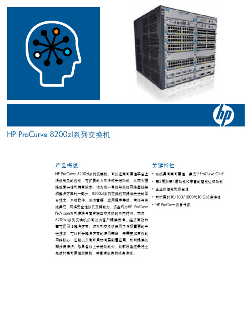
HP ProCurve 8200zl系列交换机 说明书
用RADIUS服务器对客户端进行身份验证
• RADIUS/TACACS+:使用密码验证服务器,简化交换机
- 每个端口同时进行IEEE 802.1X、Web和MAC身份验 安全性的管理流程
证:交换机端口最多可接受32个IEEE 802.1X、Web • Secure Shell (SSHv2):加密传输的所有数据,确保安全
进技术,可以延长解决方案的使用寿命,无需更加复杂的
网络核心、汇聚以及高可用访问层部署应用,即可提供长
期投资保护。除具备以上先进功能外,此款设备还是行业
先进的高可用性交换机,并享有出色的终身保修。
功能和优势
连接性
业界知名的保修服务
• 高端口密度连接性:12个接口模块插槽,每个系统有 288个支持PoE的线速10/100/1000端口,或48个10GbE端口
和MAC身份验证会话
地访问IP网络上远程命令行界面(CLI)
• 病毒遏制:无需使用外部设备,便可检测典型的蠕虫型 病毒流量模式,遏制或完全阻止病毒在VLAN或桥接口 中扩散
• DHCP保护:拦截未授权DHCP服务器发出的DHCP数据 包,避免拒绝服务攻击
• 安全的管理访问:所有访问方式(CLI、GUI或MIB)均可 通过SSHv2、SSL和/或SNMPv3安全加密
• USB Secure Autorun (需要HP ProCurve Manager Plus): 使用USB闪存盘部署、诊断并升级交换机,配合安全证 书可避免篡改
3
安全性
• 访问控制列表(ACL):根据每一个VLAN或每个端口上的 IP域、源/目标IP地址/子网和源/目标TCP/UDP端口 号,提供过滤
• STP BPDU端口保护:在不需要网桥协议数据单元(BPDU) 的端口上拦截BPDU,避免假冒BPDU攻击
STSCFCLC光纤接头区别

S T S C F C L C光纤接头区别文档编制序号:[KKIDT-LLE0828-LLETD298-POI08]ST、SC、FC、LC光纤接头区别简介:ST、SC、FC光纤接头是早期不同企业开发形成的标准,使用效果一样,各有优缺点。
ST、SC连接器接头常用于一般网络。
ST头插入后旋转半周有一卡口固定,缺点是容易折断;SC连接头直接插拔,使用很方便,缺点是容易 ...ST、SC、FC光纤接头是早期不同企业开发形成的标准,使用效果一样,各有优缺点。
ST、SC连接器接头常用于一般网络。
ST头插入后旋转半周有一卡口固定,缺点是容易折断;SC连接头直接插拔,使用很方便,缺点是容易掉出来;FC连接头一般电信网络采用,有一螺帽拧到适配器上,优点是牢靠、防灰尘,缺点是安装时间稍长。
MTRJ 型光纤跳线由两个高精度塑胶成型的连接器和光缆组成。
连接器外部件为精密塑胶件,包含推拉式插拔卡紧机构。
适用于在电信和数据网络系统中的室内应用。
光纤接口连接器的种类光纤连接器,也就是接入光模块的光纤接头,也有好多种,且相互之间不可以互用。
不是经常接触光纤的人可能会误以为GBIC和SFP模块的光纤连接器是同一种,其实不是的。
SFP模块接LC光纤连接器,而GBIC接的是SC 光纤光纤连接器。
下面对网络工程中几种常用的光纤连接器进行详细的说明:① FC型光纤连接器:外部加强方式是采用金属套,紧固方式为螺丝扣。
一般在ODF侧采用(配线架上用的最多)② SC型光纤连接器:连接GBIC光模块的连接器,它的外壳呈矩形,紧固方式是采用插拔销闩式,不须旋转。
(路由器交换机上用的最多)③ ST型光纤连接器:常用于光纤配线架,外壳呈圆形,紧固方式为螺丝扣。
(对于10Base-F连接来说,连接器通常是ST类型。
常用于光纤配线架)④ LC型光纤连接器:连接SFP模块的连接器,它采用操作方便的模块化插孔(RJ)闩锁机理制成。
(路由器常用)⑤ MT-RJ:收发一体的方形光纤连接器,一头双纤收发一体常见的几种光纤线光纤接口大全各种光纤接口类型介绍光纤接头FC 圆型带螺纹(配线架上用的最多)ST 卡接式圆型SC 卡接式方型(路由器交换机上用的最多)PC 微球面研磨抛光APC 呈8度角并做微球面研磨抛光MT-RJ 方型,一头双纤收发一体( 华为8850上有用)光纤模块:一般都支持热插拔,GBIC Giga Bitrate Interface Converter, 使用的光纤接口多为SC或ST型SFP 小型封装GBIC,使用的光纤为LC型使用的光纤:单模: L ,波长1310 单模长距LH 波长1310,1550多模:SM 波长850SX/LH表示可以使用单模或多模光纤在表示尾纤接头的标注中,我们常能见到“FC/PC”,“SC/PC”等,其含义如下“/”前面部分表示尾纤的连接器型号“SC”接头是标准方型接头,采用工程塑料,具有耐高温,不容易氧化优点。
STS8200测试系统基础培训—软件基本操作(PDF 54页)
*.mdb 【Handler】―Handler/Prober设置文件存放目录 【Lib】―专用库文件目录 【Include】―编译测试DLL用到的专用头文件 【Driver】-系统所需要的驱动存放目录
【CheckData】-系统自检后数据存放目录
AccoTest
New Valued Multi-site Analog/Mixed Signal Tester
STS 8200测试系统基础培训(3) ——软件基本操作 Rev1.0
系统软件介绍和基本操作
• 测试系统软件介绍 • 安装测试系统软件 • 软件基本操作 • 数据分析和处理
测试系统软件介绍
启动
系统自检成功后,会启动测试控制主界面,并在桌面的托盘
内显示图标
。双击图标可以弹出管理窗口 。
系统界面介绍
主界面中包含以下几部分:
工具栏:测试操作用到的功能都在工具栏中有相应的按扭 参数信息区:显示出测试参数的名称,判据,单位等信息 数据区:显示出参数的测试结果 状态栏:显示测试程序名,LOTID,操作员等信息
用户管理权限
如图红色框内可以创建3类用户,分别是:
Administrator:管理员,拥有全部操作权限 Engineer:工程师,可以编程和条件设置,不可以修改用户权限 Operator:操作员,基本操作,不能编程和条件设置。
Байду номын сангаас
自检
测试系统启动后,会首先检测测试机的状态。根据系 统配置文件检测每块电路板的基本功能是否正常,并 给出自检报告。
根据需要输入相应信息后点击OK,即可进入到待测试状态。
3. 启动测试
单次测试: 开始自动测试:
STS_8200测试系统基础培训(2)-单板介绍
coarse mode ±10ns±0.1% fine mode ±2ns±0.1% -输入电压 ±25V/±5V QTMU_PLUS -输入频率 0.1Hz -10MHz -输入时间 10ns - 40s
ACSM_PLUS
-正弦波、方波、三角波、锯齿波 -最大峰峰值 20V ;THD -80dB ACS -输出频率 0.05 KHz - 100.0 KHz -偏置电压 ±10.0 V Max
• 外观结构
• 地址开关
单通道
双通道
四通道
精密交流源表- ACSM_PLUS介绍
– SM8115精密交流源表单元(ACSM_PLUS)模块是 STS8200系统中的标准模块 – 独立的交流信号源(ACS)和精密差分交流表(ACM)支 持低速、高速、高精度交流信号测量
• 主要性能 – ACS: 每板四通道输出(共享同一AWG) – ACS: 支持正弦波、方法、三角波、锯齿波 – ACS: 正弦波输出THD可达-80db (RMS=4.0V Freq=1.0KHz) – ACM: 每板四路交流表(共享同一路AD) – ACM: 高阻抗差分输入,支持DC及AC测量 – ACM: THD测量可达-85db(正弦波RMS=4.0V Freq=1.0KHz) – ACM: 低速测试模式 200 KHz 16 Bits – ACM: 调整测试模式支持10 MHz 12 Bits
双路电压电流源- DVI400介绍
– SM8103双通道电压电流源 (DVI400)模块是STS8200 系统中的标准模块 – 共两个独立的精密四象限电压电流源,支持恒压、恒 流、测压、测流四种工作模式 – STS8200 系统最多可以安装16 个DVI400模块(共32 个通道)
STS 8200测试系统基础培训(4)—— 连接handler&proberRev1.0
注:脉冲宽度小于100us,选择Latched
Sot信号高低电平选择
设置取决于Handler发过来Sot信号,如发过来的是低电平脉冲,选择 “Negative Logic”,如发过来的是高电平脉冲,不选“Negative Logic”。
Sot低电平逻辑信号
Sot高电平逻辑信号
EOT、BIN信号高低电平选择
•
若Handler的SOT信号可以正常发出,但TTL卡没有反馈出正常的EOT和BIN 信号
如果出现这样的情况,请更换一块TTL卡进行尝试,如果通讯可以正常建立的话,那么 这块TTL卡可能出现了故障,请将此卡报修。
Prober连接与设置
• 软件设置 • 注意事项来自软件设置右图为配置 EG Prober的窗口。 下面对主要设置进行介绍。
通讯故障排除(二)
• 若+5V可以正常测量到
进入TTL信号调试界面,请在Handler上手动触发SOT信号,在TTL信号调试界面观 察,EOT和BIN信号在收到有效的SOT信号后,正常触发。需要注意的是,这个时候一 定得用示波器观察SOT信号的触发是否正常,(不正常的信号包括:Handler完全没有 触发SOT信号,或者发出的SOT信号低电平未完全拉低,高电平未完全拉高)。如果 没有收到Handler发出的正常SOT信号,那么TTL卡自然也无法反馈出正常的EOT和 BIN信号。在Handler那边无法发出正常的SOT信号的时候,建议检查一下Handler的设 置及硬件是否工作正常。 注: Signal Definition内SOT信号的设置需跟Handler实际触发的信号一致
软件设置
右图为配置Handler的窗口。 下面对主要设置进行介绍。 与Handler相关的信号主要有 三个:
DSA8200 1Series PatternSync Trigger Module数据手册说明书
PatternSync Trigger Module for the DSA8200*1Series80A06PatternSync Trigger Module DataSheetFeatures&BenefitsEnables80SJNB–The Advanced Jitter,Noise,and BER AnalysisSoftwareProvides Trigger on Repetitive Patterns from2to223Bits LongProvides Buffered Clock Output for Input to a Phase Reference Module or other DevicesAccepts Clock from Clock Recovery Circuits(CR)in the80A05and 80A07Electrical Clock Recovery Modules,and in the Optical Modules Optional SlotSaver Adapter Provides Power and Control of thePatternSync Trigger Modules,External to the Mainframe,Saving Space for Additional Channels ApplicationsWhen Used in Combination with80SJNB:Characterizing Jitter,Noise, and BER Performance of High-speed Serial Designs from1Gb/s to60Gb/s Data RatesDesign Validation and Testing of Next-generation High-speed Serial Data Computer and Communications Components and SystemsWhen Used in Combination with80SJNB:Jitter,Noise,and BERAnalysis of Multi-gigabit Standards such as Fibre Channel,OIF CEI, XFP,UXPi,SATA,PCI,Physical Layer,XAUI,Gigabit Ethernet,Rapid I/O,InfiniBand,and Other Electrical or Optical CircuitsEnables Capture of Bits in a Repetitive Pattern for Bit Analysis When Only a Clock is Available for TriggeringEnables FrameScan™of Repetitive Patterns When Only a Clock Signal is Available for TriggeringPatternSync Trigger Module80A06PatternSync Trigger module is required for the DSA8200Series when using80SJNB advanced Jitter,Noise,and BER Analysis software package.When this module is used with the82A04Phase Reference module,the jitterfloor is≤200fs RMS.The PatternSync Trigger Module is programmable to pattern lengths ofup to223bits and accepts a user-supplied clock signal from150MHzto12.75GHz.The DSA8200UI/PI for the80A06module offers pattern lengths from2to223bits and programs the module to within it's hardware range(a prescaler followed by a counter with minimum count of30)for the least-common-multiple count.Performance You Can Count OnDepend on Tektronix to provide you with performance you can count on.In addition to industry-leading service and support,this product comes backed by a three-year warranty as standard.*1Also compatible with TDS/CSA8200,TDS/CSA8000B,and TDS/CSA8000sampling oscilloscopes.Not compatible with DSA8300.Order DSA8300ADVTRIG Option for pattern synchronization in theDSA8300.Data SheetCharacteristicsCharacteristic DescriptionAcquisition Modes Standard,Triggered Phase Reference,and FrameScan™Compatible Mainframes DSA8200,TDS/CSA8200,TDS/CSA8000B,and TDS/CSA8000(Not compatible with DSA8300)Mainframe Resources Required One small(electrical)module slot,or TRIGGER PROBE POWER connector on the front panel of the oscilloscope (with available SlotSaver cable)General SpecificationsCharacteristic DescriptionInput/OutputConnectorsPrecision18GHz SMA female connectorInput and OutputImpedance50ΩAbsolute MaximumInput Voltage2.0V p-pMaximum DC Offset±5.0V DCInput Electrical Return Loss50MHz to10GHz>15dB10GHz to20GHz>10dBInput/Output CouplingClock In ACClock Out ACTrigger Out DCSupported Clock RatesMinimum150MHzMaximum12.5GHz,12.75GHz(typical) Prescaler RatiosInput clock(as selected in the UI/PI)150MHz to3.5GHz43.5GHz to7GHz87GHz to12.75GHz16Programmable Pattern LengthMinimum2Maximum223(8,388,608)Front-panel Output AmplitudesClock Out(50ΩAC coupled)150MHz to8.0GHz500mV p-p(typical)8.0GHz to12.75GHz250mV p-p(typical)Trigger Out(50ΩDC coupled,ground referenced)Output HighLevel0VOutput LowLevel–550mV(typical)Front-panel Output Rise and Fall TimesClock Out<60ps(faster for fast input slew rate)Trigger Out<60ps(faster for fast input slew rate)Characteristic DescriptionSystem JitterDSA8200,TDS/CSA8200,andTDS/CSA8000Bwith80A06<1.3ps RMS,850fs RMS(typical)TDS/CSA8000with80A06<1.6ps RMS,1.0ps RMS(typical)DSA8200andTDS/CSA8200with80A06and82A04≤200fs RMS(determined by the82A04,see82A04data sheetfor more details)Minimum InputSensitivity200mV p-pPhysical CharacteristicsDimensions mm in.Height25 1.0Width79 3.1Depth135 5.3Weight kg lb.Net0.40.6 Environmental ConditionsRefer to the host instrument specification.ElectromagneticRefer to the host instrument specification.Ordering Information80A06PatternSync Trigger Module.Includes:User manual,2each12in.SMA cables(174-1364-xx),three-year warranty.Service OptionsOption DescriptionOpt.D1Calibration Data ReportsAccessoriesAccessory Description80N01Sampling Module Extender Cable(2meter length)174-5230-xx SlotSaver Adapter Extender Cable.Bringspower andcontrol to the80A06when operated externally fromthe DSAmainframe,saving slot space(compatible with80A06and80A02)Product(s)are manufactured in ISO registered facilities.Product(s)complies with IEEE Standard488.1-1987,RS-232-C,and with TektronixStandard Codes and Formats.PatternSync Trigger Module for the DSA8200*1Series—80A06PatternSync Trigger Module3Data Sheet Contact Tektronix:ASEAN/Australasia(65)63563900Austria0080022554835*Balkans,Israel,South Africa and other ISE Countries+41526753777Belgium0080022554835*Brazil+55(11)37597627Canada180********Central East Europe and the Baltics+41526753777Central Europe&Greece+41526753777Denmark+4580881401Finland+41526753777France0080022554835*Germany0080022554835*Hong Kong4008205835India0008006501835Italy0080022554835*Japan81(3)67143010Luxembourg+41526753777Mexico,Central/South America&Caribbean52(55)56045090Middle East,Asia,and North Africa+41526753777The Netherlands0080022554835*Norway80016098People’s Republic of China4008205835Poland+41526753777Portugal800812370Republic of Korea00180082552835Russia&CIS+7(495)7484900South Africa+41526753777Spain0080022554835*Sweden0080022554835*Switzerland0080022554835*Taiwan886(2)27229622United Kingdom&Ireland0080022554835*USA180*********European toll-free number.If not accessible,call:+41526753777Updated10February2011For Further Information.Tektronix maintains a comprehensive,constantly expandingcollection of application notes,technical briefs and other resources to help engineers workingon the cutting edge of technology.Please visit Copyright©Tektronix,Inc.All rights reserved.Tektronix products are covered by U.S.and foreign patents,issued and rmation in this publication supersedes that in all previously published material.Specification and price change privileges reserved.TEKTRONIX and TEK are registered trademarks ofTektronix,Inc.All other trade names referenced are the service marks,trademarks,or registered trademarksof their respective companies.28Apr201185W-18890-5。
- 1、下载文档前请自行甄别文档内容的完整性,平台不提供额外的编辑、内容补充、找答案等附加服务。
- 2、"仅部分预览"的文档,不可在线预览部分如存在完整性等问题,可反馈申请退款(可完整预览的文档不适用该条件!)。
- 3、如文档侵犯您的权益,请联系客服反馈,我们会尽快为您处理(人工客服工作时间:9:00-18:30)。
Interface Definition for TTL Card
TTL Card is used to stablish the communication between PC and Handler
T1—T5 Setting
•T1 is the delay time of sending out BIN signal after the test finishes. The process needs no delay time usually (Suggest setting 0) •T2 is 1ms longer than T4 at least, and make sure T2 cover T4 (Handler determines the width of T2 and T4) •T3 is suggested to set between 0 and 1ms, in order to send BIN signal before EOT signal •T5 is the delay time between BIN and the next SOT (decided by Handler) •T5 is slower than Handler‟s operating time
Introduction:
•BIN : product classify information
•EOT: end of testing •SOT: start of testing
BIN and EOT are output signals(TTL Card set out to Handler) SOT is input signal(Handler set out to TTL Card) figure1
AccoTest
New Valued Multi-site Analog/Mixed Signal Tester
STS8200 Basic Training (4) -- Interface Handler & Prober Rev1.0
Interface & Setting for Handler
TTL Card Fuse
TTL Card Fuse is 0.5A
Note: If handler offers 5V itself, 5V port of TTL Card must not connect Handler .Or else it will break TTL Card Fuse
Mapping Settings Description(Ⅱ)
LocationCode select”5-8”, the setting relationship between DIE and SITE as left picture.
Mapping Settings Description(Ⅲ)
Mapping Settings Description (Ⅰ)
Tick it , then be set. Location Code: used to set the position relationship between DIE and DIE, DIE and SITE. By drop-down menu to select, the following detailed description
Export Setting button is used to save handler configure
Signal Debug Setting
1. Site and BIN choice
2. Relay time after receive the SOT
3. single test 4. Circle test
Die Size Setting Description
Tick it , then be set. WaferSize: used to set the size of Wafer through the drop-down menu. Width(Y): Set the width of DIE, units of mm. Length(X): Set the length of DIE, units of mm.
Multi-Site Synchronous Wait Time
Synchronous wait time: It is the reservation intervals after
receiving the SOT(1) during the multi-site test . If tester receives the new SOT(2) during the interval, Tester will test the sites which received the SOT(1) and SOT (2). Example: When we run a quad-site program, after receiving the first SOT(1) signal (site 1),Tester receive another SOT(3) in the synchronous wait time .Test Site(1) and Site(3) only. Note: When testing in multi-site (assumed dual site , synchronous wait time is 20ms),if TTL Card received two SOT signals in less than 20ms ,Tester run right now (NO waiting to 20th ms) .
SOT Signal Setting
Setting mode is decided by the SOT signal of Handler. If the effective signal is low level, select “Negative Logic”
SOT is low level
5. Stop test
6. Selected, tester send SOT by itself, and automatically send EOT & BIN. Interval is decided by (2)
7. Clear the window
Points for Attention
• Software setting • Points for attention
Software Setting
The setting window of EG Prober refer to the figure1.
figure1
EG Prober Connection Setting
Test Site: Station number, it‟s the test DIE number at the same time. Set it through the drop-down menu, including 1,2,4,8,16.The number should be consistent with the median of probe cards work. Address: The hardware address of the probe station.
Location Code select”9-12”, the setting relationship between DIE and SITE as left picture.
Mapping Settings Description(Ⅳ)
Coordinate Code: Used to set Prober X, Y axis direction of growth through drop-down menu, corresponding increase in the direction of the content as shown on the left picture. Mobile CHUCK, the focus Prober provided on the display X, Y coordinates, which can confirm the direction of its growth.
•TTL Card driving •TTL Card fuse
•TTL Card defining of dual station
TTL Card Driving
Pull out and insert TTL Card will make TTL fail , suggesting to install TTL driving again
Location Code select”0”, corresponding to a single station set; Location Code select”1-4”, the setting relationship between DIE and SITE as left picture.
TTL Card Defining of Dual Station
If system configuration is Dual Station, there are two TTL Cards, upper for STATION-A, below for STATION-B
Interface & Setting for Prober
Latched Function
Latched Function: defined trigger mode of receiving SOT