WB246D1100;WB24GD1100;WB24ED1100;WB242D1100;WB246D112S;中文规格书,Datasheet资料
IR2011SPBF;IR2011PBF;IR2011STRPBF;IR2011;IR2011S;中文规格书,Datasheet资料

1
/
IR2011(S) & (PbF)
Absolute Maximum Ratings
Absolute maximum ratings indicate sustained limits beyond which damage to the device may occur. All voltage parameters are absolute voltages referenced to COM. The thermal resistance and power dissipation ratings are measured under board mounted and still air conditions.
Symbol
VB VS VHO VCC VLO VIN dVs/dt PD RTHJA TJ TS TL
Definition
High side floating supply voltage High side floating supply offset voltage High side floating output voltage Low side fixed supply voltage Low side output voltage Logic input voltage (HIN & LIN) Allowable offset supply voltage transient (figure 2) Package power dissipation @ TA £ +25°C Thermal resistance, junction to ambient Junction temperature Storage temperature Lead temperature (soldering, 10 seconds) (8-lead DIP) (8-lead SOIC) (8-lead DIP) (8-lead SOIC)
170M1560D,170M1562D,170M1563D,170M1565D,170M1566D,170M1564D,170M1569D, 规格书,Datasheet 资料

Standards/Approvals:CE, designed and tested to IEC 60269: part4. UL recognised (Survival Only), CSADescription:Square body DIN 43620 blade style, dualindication High Speed fusesPackaging:Size 000 are packed in 10’sSize 00 are packed in 6’sTechnical Data:Rated Voltage:690 VacAmps:10A to 315ARated Breaking Capacity: 200kA RMS SymRoHS Compliant: YesCatalogue Symbol:170M1558D to 170M1572DClass of Operation:gR (10 to 63A), aR (80 to 315A)Dimensional Data:DIN 000 Type T1mm = 0.0394” / 1” = 25.4mm DIN 00 Type T1mm = 0.0394” / 1” = 25.4mmCatalogue Numbers:Standard Approvals:CE, IEC 60269: part 4, UL recognised (Survival Only), CSATechnical Data:10, 16, 20, 25, 25, 32, 40, 50, 63, 80, 100, 125, 160, 200, 250, 315* Amps*315A is only available in size DIN00The rated current of this fuse range has been given with copper conductors that have a high current density of 1.3A/mm 2(IEC 60269-4). For conductor cross section according to IEC 60269-1, the fuses with a rated current higher than 125A must be derated. Please contact Cooper Bussmann for application assistance.Total Clearing I 2TThe total clearing I 2t at rated voltage and at power factor of 15% are given in the electrical characteristics. For other voltages, the clearing I 2t is found by multiplying by correction factor, K, given as a function of applied working voltage Eg (rms)Power LossesWatts loss at rated current is given in the electrical characteristics. The curve allows the calculation of the power losses at load currents lower than the rated current. The correction factor, Kp, is given as a function of the RMS load current, lb, in % of the ratedcurrent.This curve gives the peak arc voltage, UL,which may appear accross the fuse during its operation as a function of the applied working voltage, Egrection factor, K, given as afunction of applied working voltage Eg (rms)at a power factor of 15%Time Current CurvesPeak Let-Through。
LAA110LSTR;LAA110LS;LAA110L;中文规格书,Datasheet资料

Approvals
• UL Recognized Component: File # E76270 • CSA Certified Component: Certificate # 1175739 • EN/IEC 60950-1 Certified Component: TUV Certificate B 09 07 49410 004
Typical Blocking Voltage Distribution (N=50, TA=25ºC)
Turn-Off (ms)
Turn-On (ms)
25 20 15 10 5 0 376.3 382.8 389.3 395.8 402.3 408.8 415.3 Blocking Voltage (VP)
1 2
Conditions VL=8V, IF=5mA IL=120mA VL=350VP
Symbol IL ICL RON ILEAK ton toff COUT IF VF IR CI/O
Min 130 0.4 0.9 -
Typ 170 30 25 0.7 1.2 3
Max 120 210 35 1 3 3 5 1.4 10 -
Device Count (N)
Device Count (N)
0.45
0.75
1.05 1.35 1.65 1.95 LED Current (mA)
2.25
17.0
17.4
17.8 18.2 18.6 19.0 On-Resistance (Ω)
19.4
35 30 Device Count (N)
Pin Configuration
+ Control - Switch #1 – Control - Switch #1 + Control - Switch #2 – Control - Switch #2 1 2 3 4 8 7 6 5 Load - Switch #1 Load - Switch #1 Load - Switch #2 Load - Switch #2
SK24-TP;SK22-TP;SK210-TP;SK23-TP;SK25-TP;中文规格书,Datasheet资料
50 100
Figure 4 New SMB Assembly
.2
.1 0 .2 .4 .6 .8 1.0 1.2 1.4 Volts
Instantaneous Forward Current - Amperesversus Instantaneous Forward Voltage - Volts
IF(AV) IFSM
VF IR
2.0A 50A
TJ = 90°C 8.3ms, half sine
.55V .70V .85V
IFM = 2.0A; TJ = 25°C*
TJ = 25°C
0.5 mA
Typical Junction
CapacitanceSFra bibliotek22CJ
SK23-SK210
230pF Measured at 50pF 1.0MHz, VR=4.0V
*Pulse test: Pulse width 300 µsec, Duty cycle 2%
Note: 1. High Temperature Solder Exemptions Applied, see EU Directive Annex 7.
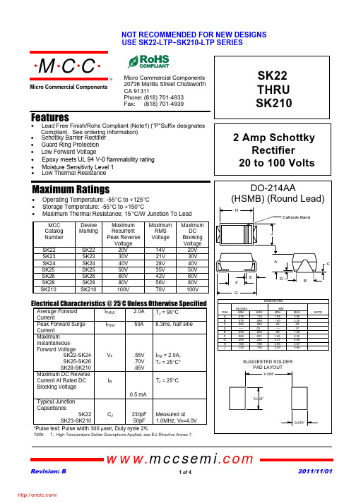
SK22 THRU SK210
2 Amp Schottky Rectifier
50 100
Figure 4 New SMB Assembly
.2
.1 0 .2 .4 .6 .8 1.0 1.2 1.4 Volts
Instantaneous Forward Current - Amperesversus Instantaneous Forward Voltage - Volts
Figure 3 Typical Junction Capacitance 10000 6000
半导体传感器ADUM2402BRWZ中文规格书
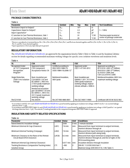
Data SheetADuM1400/ADuM1401/ADuM1402 Rev. L | Page 19 of 31PACKAGE CHARACTERISTICS Table 8.ParameterSymbol Min Typ Max Unit Test Conditions Resistance (Input to Output)1R I-O 1012 Ω Capacitance (Input to Output)1C I-O 2.2 pF f = 1 MHz Input Capacitance 2C I 4.0 pF IC Junction to Case Thermal Resistance, Side 1θJCI 33 °C/W Thermocouple located at center of package underside IC Junction to Case Thermal Resistance, Side 2θJCO 28 °C/W 1 Device is considered a 2-terminal device; Pin 1, Pin 2, Pin 3, Pin 4, Pin 5, Pin 6, Pin 7, and Pin 8 are shorted together and Pin 9, Pin 10, Pin 11, Pin 12, Pin 13, Pin 14, Pin 15, and Pin 16 are shorted together.2 Input capacitance is from any input data pin to ground.REGULATORY INFORMATIONThe ADuM1400/ADuM1401/ADuM1402 are approved by the organizations listed in Table 9. Refer to Table 14 and the Insulation Lifetime section for details regarding recommended maximum working voltages for specific cross-isolation waveforms and insulation levels. Table 9.ULCSA VDE CQC TÜV Recognized Under UL 1577 Component RecognitionProgram 1 Approved under CSA Component Acceptance Notice 5A Certified according to DIN V VDE V 0884-10 (VDE V 0884-10):2006-122 Approved under CQC11-471543-2012 Approved according to IEC 61010-1:2001 (2nd Edition), EN 61010-1:2001 (2nd Edition),UL 61010-1:2004, andCSA C22.2.61010.1:2005Single Protection, 2500 V rms Isolation Voltage Basic insulation per CSA 60950-1-03 and IEC 60950-1, 780 V rms (1103 V peak) maximumworking voltageReinforced insulation, 560 V peak Basic Insulation per GB4943.1-2011, 415 V rms (588 V peak) maximum working voltage, tropical climate, altitude ≤ 5000 m Reinforced insulation, 400 V rmsmaximum working voltage Reinforced insulation per CSA 60950-1-03 andIEC 60950-1, 390 V rms(551 V peak) maximumworking voltageFile E214100 File 205078 File 2471900-4880-0001File CQC14001114900 Certificate U8V 05 06 56232 002 1 In accordance with UL 1577, each ADuM1400/ADuM1401/ADuM1402 is proof tested by applying an insulation test voltage ≥3000 V rms for 1 sec (current leakage detection limit = 5 µA).2 In accordance with DIN V VDE V 0884-10, each ADuM1400/ADuM1401/ADuM1402 is proof tested by applying an insulation test voltage ≥1050 V peak for 1 sec (partial discharge detection limit = 5 pC). The asterisk (*) marking branded on the component designates DIN V VDE V 0884-10 approval.INSULATION AND SAFETY RELATED SPECIFICATIONSTable 10.ParameterSymbol Value Unit Conditions Rated Dielectric Insulation Voltage2500 V rms 1-minute duration Minimum External Air Gap (Clearance)L(I01) 7.8 min mm Measured from input terminals to output terminals, shortest distance through air Minimum External Tracking (Creepage)L(I02) 7.8 min mm Measured from input terminals to output terminals, shortest distance path along body Minimum Clearance in the Plane of the PrintedCircuit Board (PCB Clearance)L(PCB) 8.3 min mm Measured from input terminals to output terminals, shortest distance through air, and line of sight, in the PCB mounting plane Minimum Internal Gap (Internal Clearance)0.017 min mm Insulation distance through insulation Tracking Resistance (Comparative Tracking Index)CTI>400V DIN IEC 112/VDE 0303 Part 1 Isolation Group II Material Group (DIN VDE 0110, 1/89, Table 1)ADuM1400/ADuM1401/ADuM1402Data Sheet Rev. L | Page 22 of 31PIN CONFIGURATIONS AND FUNCTION DESCRIPTIONSV DD1*GND 1V IA V IB V DD2GND 2*V OA V OB V IC V OC V ID V OD NC V E2*GND 1GND 2*NC = NO CONNECT03786-005*PIN 2 AND PIN 8 ARE INTERNALLY CONNECTED, AND CONNECTING BOTH TO GND 1 IS RECOMMENDED. PIN 9 AND PIN 15 ARE INTERNALLY CONNECTED, AND CONNECTING BOTH TO GND 2 IS RECOMMENDED.Figure 5. ADuM1400 Pin Configuration Table 16. ADuM1400 Pin Function DescriptionsPin No.Mnemonic Description 1V DD1 Supply Voltage for Isolator Side 1. 2GND 1Ground 1. Ground reference for Isolator Side 1. 3V IA Logic Input A. 4V IB Logic Input B. 5V IC Logic Input C. 6V ID Logic Input D. 7NC No Connect. 8GND 1 Ground 1. Ground reference for Isolator Side 1. 9GND 2 Ground 2. Ground reference for Isolator Side 2. 10V E2 Output Enable 2. Active high logic input. V OA , V OB , V OC , and V OD outputs are enabled when V E2 is high or disconnected. V OA , V OB , V OC , and V OD outputs are disabled when V E2 is low. In noisy environments, connecting V E2 to an external logic high or low is recommended. 11V OD Logic Output D. 12V OC Logic Output C. 13V OB Logic Output B. 14V OA Logic Output A. 15GND 2Ground 2. Ground reference for Isolator Side 2. 16 V DD2 Supply Voltage for Isolator Side 2.。
STGW40N120KD;中文规格书,Datasheet资料

February 2012Doc ID 15360 Rev 51/15STGW40N120KD STGWA40N120KD40 A, 1200 V short circuit rugged IGBT with Ultrafast diodeFeatures■Low on-losses ■High current capability ■Low gate charge■Short circuit withstand time 10 µs■IGBT co-packaged with Ultrafast free-wheeling diodeApplications■Motor controlDescriptionThis high voltage and short-circuit rugged IGBT utilizes the advanced PowerMESH™ process resulting in an excellent trade-off between switching performance and low ON-state behavior.Table 1.Device summaryOrder codes Markings Package Packaging STGW40N120KD GW40N120KD TO-247Tube STGWA40N120KDGWA40N120KDTO-247 long leadsTubeContents STGW40N120KD, STGWA40N120KDContents1Electrical ratings . . . . . . . . . . . . . . . . . . . . . . . . . . . . . . . . . . . . . . . . . . . . 32Electrical characteristics . . . . . . . . . . . . . . . . . . . . . . . . . . . . . . . . . . . . . 42.1Electrical characteristics (curves) . . . . . . . . . . . . . . . . . . . . . . . . . . . . 6 3Test circuits . . . . . . . . . . . . . . . . . . . . . . . . . . . . . . . . . . . . . . . . . . . . . . . 9 4Package mechanical data . . . . . . . . . . . . . . . . . . . . . . . . . . . . . . . . . . . . 10 5Revision history . . . . . . . . . . . . . . . . . . . . . . . . . . . . . . . . . . . . . . . . . . . 142/15 Doc ID 15360 Rev 5STGW40N120KD, STGWA40N120KD Electrical ratingsDoc ID 15360 Rev 53/151 Electrical ratingsTable 2.Absolute maximum ratingsSymbol ParameterValue Unit V CES Collector-emitter voltage (V GE = 0)1200V I C (1)1. Calculated according to the iterative formula:Continuous collector current at T C = 25 °C 80A I C (1)Continuous collector current at T C = 100 °C 40A I CL (2)2.Vclamp = 80% of V CES , T j =125 °C, R G =10 Ω, V GE =15 VTurn-off latching current 85A I CP (3)3. Pulse width limited by maximum junction temperature and turn-off within RBSOAPulsed collector current 120A V GE Gate-emitter voltage±25V t SCW Short circuit withstand time, V CE = 0.5 V (BR)CEST j = 125 °C, R G = 10 Ω, V GE = 12 V 10µs P TOT Total dissipation at T C = 25 °C240W I F Diode RMS forward current at T C = 25 °C 30A I FSM Surge non repetitive forward current t p = 10 ms sinusoidal100A T jOperating junction temperature– 55 to 125°CTable 3.Thermal dataSymbol ParameterValue Unit R thj-case Thermal resistance junction-case IGBT 0.42°C/W R thj-case Thermal resistance junction-case diode 1.6°C/W R thj-ambThermal resistance junction-ambient50°C/WI C T C ()T j max ()T C–R thj c –V CE sat ()max ()T j max ()I C T C (),()×-------------------------------------------------------------------------------------------------------=Electrical characteristics STGW40N120KD, STGWA40N120KD4/15 Doc ID 15360 Rev 52 Electrical characteristicsT J = 25 °C unless otherwise specified.Table 4.StaticSymbolParameterTest conditions Min.Typ.Max.Unit V (BR)CES Collector-emitterbreakdown voltage(V GE = 0)I C = 1 mA1200V V CE(sat)Collector-emitter saturationvoltageV GE = 15 V , I C = 30 AV GE = 15 V , I C = 30 A,T J =125 °C 2.82.73.85V V V GE(th)Gate threshold voltage V CE = V GE , I C = 1mA 4.56.5V I CES Collector cut-off current (V GE = 0)V CE =1200 VV CE =1200 V , T J =125 °C 50010µA mA I GESGate-emitter leakage current (V CE = 0)V GE =± 20 V± 100nATable 5.DynamicSymbol ParameterTest conditionsMin.Typ.Max.Unit C ies C oes C res Input capacitance Output capacitance Reverse transfer capacitanceV CE = 25 V , f = 1 MHz, V GE =0-257719639.5-pF pF pF Q g Q ge Q gcTotal gate charge Gate-emitter charge Gate-collector chargeV CE = 960 V ,I C = 30 A,V GE =15 V-12622.267-nC nC nCTable 6.Switching on/off (inductive load)Symbol ParameterTest conditions Min.Typ.Max.Unit t d(on)t r (di/dt)on Turn-on delay time Current rise timeTurn-on current slope V CC = 960 V , I C = 30 A R G = 10 Ω, V GE = 15 V , (see Figure 16)-4840540-ns ns A/µs t d(on)t r (di/dt)on Turn-on delay time Current rise timeTurn-on current slope V CC = 960 V , I C = 30 A R G = 10 Ω, V GE = 15 V ,T J = 125 °C (see Figure 16)-4538665-ns ns A/µs t r (V off )t d (off )t f Off voltage rise time Turn-off delay time Current fall time V CC = 960 V , I C = 30 A R G = 10 Ω, V GE = 15 V , (see Figure 16)-84338210-ns ns ns t r (V off )t d (off )t fOff voltage rise time Turn-off delay time Current fall timeV CC = 960 V , I C = 30 A R G = 10 Ω, V GE = 15 V ,T J = 125 °C (see Figure 16)-144420360-ns ns nsSTGW40N120KD, STGWA40N120KD Electrical characteristicsDoc ID 15360 Rev 55/15Table 7.Switching energy (inductive load)Symbol ParameterTest conditions Min.Typ.Max.Unit Eon (1)E off (2)E ts 1. Eon is the turn-on losses when a typical diode is used in the test circuit in Figure 16. If the IGBT is offeredin a package with a co-pack diode, the co-pack diode is used as external diode. IGBTs and diode are at the same temperature (25°C and 125°C)2.Turn-off losses include also the tail of the collector currentT urn-on switching losses T urn-off switching losses T otal switching losses V CC = 960 V , I C = 30 A R G =10 Ω, V GE = 15 V , (see Figure 16)- 3.75.79.4-mJ mJ mJ Eon (1)E off (2)E tsT urn-on switching losses T urn-off switching losses T otal switching lossesV CC = 960 V , I C = 30 A R G =10 Ω, V GE = 15 V ,T J = 125 °C (see Figure 16)- 4.79.314-mJ mJ mJTable 8.Collector-emitter diodeSymbol ParameterTest conditions Min.Typ.Max.Unit V F Forward on-voltage I F = 20 AI F = 20 A, T J = 125 °C - 1.91.7-V V t rr Q rr I rrm Reverse recovery time Reverse recovery charge Reverse recovery current I F = 20 A, V R = 45 V ,di/dt = 100 A/µs (see Figure 19)-842355.6-ns nC A t rr Q rr I rrmReverse recovery time Reverse recovery charge Reverse recovery currentI F = 20 A, V R = 45 V ,T J = 125 °C, di/dt = 100 A/µs (see Figure 19)-1527229-ns nC AElectrical characteristics STGW40N120KD, STGWA40N120KD6/15 Doc ID 15360 Rev 52.1 Electrical characteristics (curves)Figure 4.Collector-emitter on voltage vs.Figure 5.Collector-emitter on voltage vs. Figure 6.Gate charge vs. gate-sourceFigure 7.Capacitance variationsSTGW40N120KD, STGWA40N120KD Electrical characteristicsDoc ID 15360 Rev 57/15Figure 8.Normalized gate threshold voltageFigure 9.Normalized breakdown voltage vs. Figure 10.Switching losses vs. collectorFigure 11.Switching losses vs. gateElectrical characteristics STGW40N120KD, STGWA40N120KD Figure 14.Turn-off SOA Figure 15.Forward voltage drop vs. forward8/15 Doc ID 15360 Rev 5STGW40N120KD, STGWA40N120KD Test circuitsDoc ID 15360 Rev 59/153 Test circuitsFigure 16.Test circuit for inductive loadFigure 17.Gate charge test circuitPackage mechanical data STGW40N120KD, STGWA40N120KD 4 Package mechanical dataIn order to meet environmental requirements, ST offers these devices in different grades ofECOP ACK® packages, depending on their level of environmental compliance. ECOPACK®specifications, grade definitions and product status are available at: . ECOPACKis an ST trademark.Table 9.TO-247 mechanical datamm.Dim.Min.Typ.Max.A 4.85 5.15A1 2.20 2.60b 1.0 1.40b1 2.0 2.40b2 3.0 3.40c0.400.80D19.8520.15E15.4515.75e 5.30 5.45 5.60L14.2014.80L1 3.70 4.30L218.50∅P 3.55 3.65∅R 4.50 5.50S 5.30 5.50 5.7010/15 Doc ID 15360 Rev 5分销商库存信息: STMSTGW40N120KD。
ED5552DS;ED5553DS;ED5554DS;ED5555DS;ED5556DS;中文规格书,Datasheet资料
2-16 poles, Spacing 3.5 minsert required no. of polesHow to order see pag
Ratings:Rated Voltage 150 V 130 VRated Current 6 A 13.5 A (Wire Size AWG 28-16 1.0 mmTest Voltage 2.0 kV
Rated Torque/ScrewSize 0.4 Nm
Max. Rated Cross SectionSingle Wire (solid) 1.5 mmStranded Wire (flexible) 1.5 mm
Stranded wire with Ferrules 0.75 mm
Dimensions Spacing 3.5 mm
PCB Hole Diameter 1.2 mm
Stripped Length 5.5 mm
MaterialsInsulating Material PAFlammability Class UL94 VTemperature Range -30 C/+Terminal Block CuZn
Wire Guard Stainle
ColorGrey 分销商库存信息:ON-SHORE-TECHNOLOGY
ED555/2DSED555/3DSED555/4DS
ED555/5DSED555/6DSED555/7DS
ED555/8DSED555/9DSED555/10DS
ED555/12DSED555/14DSED555/16DS
ED555/11DSED555/3DS-BUED555/12DS-BU
LT1166CN8;LT1166CN8#PBF;LT1166CS8#PBF;LT1166CS8;LT1166CS8#TR;中文规格书,Datasheet资料
0.13
mho
0.16
mho
0.16
mho
dB
dB
1.5
V
– 1.5
V
The q denotes specifications which apply over the full operating temperature range.
Note 1: External power devices may require heat sinking.
100
50
ITOP = IBOTTOM = 50mA
0 ITOP = IBOTTOM = 4mA
LT1166
Power Output Stage Automatic Bias System
+ +
U
U
FEATURES
s Set Class AB Bias Currents s Eliminates Adjustments s Eliminates Thermal Runaway of IQ s Corrects for Device Mismatch s Simplifies Heat Sinking s Programmable Current Limit s May Be Paralleled for Higher Current s Small SO-8 or PDIP Package
Note 8: PSRRCC = gmCC2 – gmCC10
gm CC2 PSRREE = gmEE2 – gmEE10
gm EE2 Note 9: For Linear Operation, Pin 1 must not be less than 2V or more than 10V from Pin 3. Similarly, Pin 4 must not be less than 2V or more than 10V from Pin 3.