ESD Training Material for Tape Head
35344-001_P_001希捷测试方法
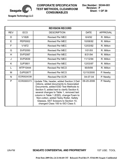
REVISION RECORDREV ECO DESCRIPTION DATE APPROVALD V1828 Revised Per MEC 6/4/92 R. MiltonE PEP0002 Revised Per MEC 10/08/92 R. MiltonF V1872 Revised Per MEC 12/03/92 R. MiltonG SVP2050 Revised Per MEC 1/01/93 R. MiltonH SVP2087 Revised Per MEC 8/31/94 R. Milton J SVP2839 Revised Per MEC 11/12/94 R. Milton K SJP3801 Revised Per MEC 12/03/97 R. Milton L WTP10444 Revised Per MCO 90/9/99 R. Milton M DJP02677 Revised Per MCO 12/15/2000 P. Newby N ECR0024338 Revised Per ECR 04-07-04 P. Newby09-20-2006 P. Newby P ECR0065373 Update Title, header, added Section 3 Def-initions, added documents to AssociatedDocuments, added ESD Test Methods toSection 5, added text to clarify Section 6,several changes to T able 1, removed lastcolumn in Table 1 (ESD), change Foam toNon-cotton, added T acky Roller, SafetyGlasses, SST Scissors to Section 10,changed Class 100 to ISO Class 5.TABLE OF CONTENTS1 PURPOSE (3)2 SCOPE (3)3 DEFINITIONS (3)4 ASSOCIATED DOCUMENTS (4)5 TOOLS AND EQUIPMENT (5)6 SAMPLE QUANTITY AND SIZES OF ITEMS TO BE TESTED (6)7 SAFETY PRECAUTIONS (11)8 SAMPLE PREPARATION (NVR/INORGANIC ION) (13)9 NON-VOLATILE RESIDUE (NVR) TEST METHOD (15)10 RESIDUE ANALYSIS PROCEDURE (FTIR) (18)11 INORGANIC ION TEST METHOD (ION CHROMATOGRAPHY) (20)12 PARTICLE COUNT MEASUREMENT (A): Helmke Drum Test (21)13 PARTICLE COUNT MEASUREMENT (B): Liquid Particle Count (23)14 PARTICLE COUNT MEASUREMENT (C): Bags Only (26)15 SEM/EDX ANALYSIS OF MAGNESIUM SILICATE: GLOVES (29)16 85/85 ENVIRONMENTAL TESTING METHOD (31)17 OUTGASSING TEST (33)APPENDIX A - GARMENT FTIR TESTING (34)1 PURPOSETo establish measurements methods for cleanliness qualification of Cleanroom Consumables (for example: gloves, swabs, wipes, pens, paper, and so on) and consumable items used for specific assembly processes that may have the potential of contaminating a Seagatecomponent or assembly.2 SCOPETo provide world wide guidelines for measuring cleanliness of cleanroom consumables and other specific consumable items as delivered by suppliers.3 DEFINITIONSCleanroom Consumable: A Cleanroom consumable is a production indirect material that must be qualified for use in a Cleanroom environment. It has a limited life or is consumed as part ofa Cleanroom process or procedure. Due to differing requirements for cleanliness which dependupon the use of the Cleanroom consumable or other consumable item, they are divided into four categories:Category 1: Cleanroom consumables that come in contact with HGA/HSA/HDAAssemblies.Category 2: Cleanroom consumables that are in close proximity to HGA/HSA/HDAAssemblies.Category 3: Cleanroom consumables used in the Cleanroom that do not come incontact with HGA/HSA/HDA Assemblies.Category 4: Consumable items (not limited to Cleanroom) used for a specificassembly process, that may have the potential of contaminating aSeagate component or assembly.4 ASSOCIATED DOCUMENTSST1027 CSOP, EOS/ESD Control Program SpecificationST1102 CSOP, Corporate Cleanroom Consumables New Item Request ProcessST1248 ESD Standard Test Method Test Procedures for Qualification of Equipment and Materials30228-001 Spec, Supplier Packaging Standard30825-001 Corporate Specification, Tape/Labels, Cleanroom35348-001 Specification Swabs, Non Cotton35350-001 Specification Swabs, Cotton35355-XXX Corporate Specification, Paper/Notebook35357-XXX Corporate Specification, Pen, Marking & Ballpoint Cleanroom35359-001 Corporate Specification, Wipes, Cleanroom35366-001 Specification, Gloves Cleanroom35368-001 Specification Headcover, Disposable, Cleanroom35370-XXX Corporate Specification, HeadCover, Launderable, Cleanroom35373-XXX Corporate Specification, Smock/Frock Launderable Cleanroom35374-XXX Corporate Specification, Coveralls, Launderable, Cleanroom35375-001 Corporate Specification, Disposable Facecover, Cleanroom Specification 35376-XXX Specification, Disposable Shoe Cover, Cleanroom35378-XXX Specification, Shoe Cover, Launderable, Cleanroom35391-001 Corporate Specification, Mat, Tacky/Disposable Cleanroom35424-XXX Specification, Mat, Workstation, ESD, Cleanroom35555-008 Test Method, Total Extractable Tin by Inductively Coupled Mass Spectroscopy (ICP-MS)35581-001 Specification, Syringe, Epoxy/Dispensing Cleanroom100164562 Specification, Tweezers & Scissors, Cleanroom100175932 Corporate Specification, Filter-Aqueous Cleaning Systems100180375 Corporate Specification, Tacky Roller100180376 Corporate Specification, Machineable ESD Material100180377 Specification, Wrist Strap or Grounding Cord100195732 Corporate Specification, Coveralls, Hooded, Launderable, Cleanroom D0000042553 Corporate Spec, Bottle, Dispensing, ESD DissipativeD0000084531 Specification, ESD Protection & Cleanliness BagD0000089017 Corporate Specification, Safety Glasses, CleanroomD0000103839 Specification, MHT Clockhead HGA Tray, Foam Insert, CleanroomD0000104558 Specification, Cleanliness Swage Ball, CleanroomD0000130724 Specification, Mop Head, CleanroomD0000150378 Corporate Specification, Face Veil, Launderable, Cleanroom 20800012-001 Spec, W/W Method, Ionic Contamination Analysis Procedure 20800014-001 Method, W/W Non-volatile Residue and Silicone Oil Analysis 20800020-001 Worldwide Method for Dynamic Headspace Outgassing20800032-001 Method, W/W Quantitative Analysis of Organic Contamination 20800033-001 Spec, Cleanliness, Plastic Parts20800040-001 Method, W/W Liquid Particle Analysis64794880 Tray Material Qualification81453598 Pole Tip Corrosion AuditCC003.3 IEST-RP-CC003.3: Garment System Considerations5 TOOLS AND EQUIPMENT5.1 Non-Volatile Residue (NVR) MeasurementRefer to 20800014-001 Method, W/W Non-volatile Residue and Silicone Oil Analysisfor equipment and set up.5.2 FTIR AnalysisRefer to 20800032-001 Method, W/W Quantitative Analysis of Organic Contamination forequipment and set up for FTIR.5.3 Particle Count Measurement• Method A: Helmke Drum TestRefer to IEST-RP-CC003.3: Gowning of Personnel in Cleanroom Contamination Control,section B2.5 Helmke Drum Test (Woven, Nonwoven, and Coated Fabrics) for equipmentand set up.•Method B: LPC (Liquid Particle Count)Refer to 20800040-001 Method, W/W Liquid Particle Analysis for equipment and set up forLPC.•Method C: LPC for Bags OnlyRefer to 20800040-001 Method, W/W Liquid Particle Analysis for equipment for LPC.Refer to section 13.3 of this document for specific sample extraction method for Bags. 5.4 Inorganic Ion Measurement (Ion Chromatograph)Refer to 20800012-001 Spec, W/W Method, Ionic Contamination Analysis Procedure 5.5 SEM/EDX Analysis• Refer to manual for Scanning Electron Microscope with Energy Dispersive X-ray attachment • Ultrasonic Tank, approximate size 9" x 6" x 6" deep, 45 kHz5.6 85/85 Environmental AnalysisRefer to Process number: 81453598, Pole Tip Corrosion Audit for equipment and set up.5.7 Outgassing AnalysisRefer to 20800020-001 Worldwide Method for Dynamic Headspace Outgassing forequipment and set up.5.8 ESD Test Methods for ConsumablesReference CSOP ST1248 using Method STxxxx, for consumable items listed:ST1248 ESD Standard Test Method Test Procedures for Qualification of Equipment and Materials Method ST1231 ESD Homogeneous Plastic Raw and Finished Material QualificationStandard T est MethodMethod ST1234 ESD Garment Qualification Standard Test MethodMethod ST1235 ESD Glove Qualification Standard Test MethodMethod ST1237 ESD Consumable Item Qualification Standard T est MethodMethod ST1241 ESD Tweezer Qualification Standard T est MethodMethod ST1242 ESD Wriststrap Assembly Qualification Standard Test MethodMethod ST1243 ESD Footwear Qualification Standard T est MethodMethod ST1246 ESD Worksurfaces and Floor Mats Qualification Standard T est Method D0000084531 Specification, ESD Protection and Cleanliness, Bags - Sample Qty: 606 SAMPLE QUANTITY AND SIZES OF ITEMS TO BE TESTEDFor sample quantities and sizes needed for each test, see T able 1 and Table 2. All tests listed must be completed. In general, three different lot shipments must meet the specification to qualify a supplier’s product, especially the high volume consumables, such as bags, gloves, swabs, wipes, and paper. In cases where the manufacture of an item produces many years worth of parts, (such as many machinable materials and newly developed, custom materials, or tweezers with replaceable tips), or when the cost of an item is prohibitive, (for example,aqueous filters or high cost wipes), Corporate Contamination can allow less than three lots for qualification.Durable Consumable items, such as Safety Glasses, where multiple models or sizes made from the same materials and with the same process are to be tested, can approximate 3 lots using each model (siz e) as 1 “lot” when 3 or more models (sizes) are to be tested, or 2 lots of one model (size) plus 1 lot of the second model (size) if 1 or 2 models (sizes) are to be tested.A memo of justification for Corporate Contamination’s approval is required p rior to testing ofless than three lots. Lot definitions will vary from manufacturer to manufacturer. For purposes of this specification, lots will be defined by production date if the supplier lacks a lot numbering system. Thus, each different production date may be used to represent a different lot.CORPORATE SPECIFICATION TEST METHODS, CLEANROOM CONSUMABLESDoc Number: Revision: Sheet: 35344-001 P 9 OF 39Seagate Technology LLCUN-FM SEAGATE CONFIDENTIAL AND PROPRIETARY 1ST USE: TOOLPrint Date:2009-Dec-24 21:04:48 CST Released; Prod Rel; P; 35344-001 Seagate ConfidentialTABLE 1: Sample Quantities Needed Per Lot for Extractions and 85/85 Corrosion, and ESD Test MethodsConsumable Item to be testedD.I. Water Extractions for Ions (IC) andNVR(may use same sample for both IC andNVR in D.I. Water)IPA, Acetone or IPA(50%)/hexane(50%)Extractions for NVRFTIR & Outgassing 85/85 Testing per Proc. No. 81453598(2) ESD Test MethodQty per Lot Qty needed per test # of tests DI Water Volume pertest Qty per Lot Qty needed per test # of tests Solvent Volume pertestSolvent Volume needed forFTIRQty needed (samples /sliders)Aqueous Cleaning System FiltersInner & Outer Mesh/ Cage:Min. of27-42g Media: Min. of18-30g O-ring: 2Inner & Outer Mesh/ Cage: 9-14gr Media: 6-10gr O-ring: 1/2 per test340 mlInner & Outer Mesh/ Cage: Min. of27-42g Media: Min. of18-30g O-ring: 2Inner & Outer Mesh/ Cage: 9- 14gr Media: 6-10gr O-ring: 1/2 per test340 mlFTIR:Outer cage/mesh: 20ml hexane rinseMedia:5 min soak in 10 ml hexaneO-ring (use O-ring that arrivesinstalled on filter):5 min soak in 10 ml hexane--BagMin. of 31350 ml (1)Min. of 31350 ml IPA/ hexaneFTIR: < 20 ml IPA/hexaneOutgassing: Min. of1 sq.in. (6.5 cm 2)Min. of 5 bags 50 slidersD00000- 84531Epoxy Dispensing ComponentsMin. of 6 - 9 g2 -3 g340 mlMin. of 6 - 9 g2 -3 g340 ml IPAFTIR: < 20 ml Hexane rinse1 or2 large pieces or 10 small pieces / 25 slidersST1248: MethodST1237Beard or Face Veil,launderable--------FTIR: see Appendix A 5 Beard Covers or Face Veils-ST1248: Method ST1234GlovesMin. of 313100 mlMin. of 313100 ml IPA/ hexane FTIR: Min. of 12 finger 25 ml hexane rinse-ST1248: Method ST1235Garments, launderable--------FTIR: see Appendix AMin. of 1 Coveralls w/ Hood or1 Coverallsor1 Smock/Frock-ST1248: Method ST1234Head Cover, launderable-------- FTIR: see Appendix A Min. of 1 Head Cover-ST1248: Method ST1234Consumable Item to betested D.I. Water Extractions for Ions (IC) and NVR(may use same sample for both IC and NVRin D.I. Water)IPA, Acetone or IPA(50%)/hexane(50%)Extractions for NVR FTIR & Outgassing85/85 Testingper Proc. No.81453598(2)ESDTestMethod Qty perLotQty neededper test# oftestsDI WaterVolume pertestQty perLotQty neededper test# oftestsSolventVolume pertestSolvent Volume needed for FTIR Qty. needed(samples/sliders)Labels/Tape(not part of drive)(3)Min. of 1.5g 0.5 g 310 ml(IC only)----FTIR: Min. of 20 cm2Labels or Tape< 20 ml IPA/hexanerinse each surfaceOutgassing: See 20800020-001Min. of 6-12labels or tapeequiv. / 25slidersST1248:MethodST1237Machinable Material, ESD Min. of60cm2 20 cm2 320 ml(IC only)Min. of60cm2 20 cm2 310 ml ofeach:IPA, Hexane,AcetoneUse:100180376FTIR: Min. of 20cm220 ml hexane rinse1 sample / 25slidersST1248:MethodST1231Mats,ESD Workstation Min. of 6 g 2 g310 ml(IC only)----FTIR: Min. 1 Mat< 20 ml hexane rinse1 mat / 25slidersST1248:MethodST1246Mats, Tacky(7)--------FTIR: Min. 200 cm210 ml hexane rinseOutgassing: See 20800020-001-ST1248:MethodST1246Mop Heads --------210 ml hexane rinse-ST1248:MethodST1237Paper Min. of 3 g 1 g310 ml(IC only)----FTIR: Min. of 1 sheet30 ml hexane rinse / 100 cm2paper surfaceMin. of 1 sheet/ 25 slidersST1248:MethodST1237Pen/MarkerBody--------FTIR: Min. of 2< 20 ml hexane rinseFor non-metalpen bodiesonly: 1 pen / 25slidersST1248:MethodST1237Pen/MarkerInk--------Outgassing: Consult STLM Labon ink quantityInk with 50sliders total -Consumable Plastic Parts (Zip Ties, BadgeHolders, etc.)Min. of60 cm2surfacearea2surfacearea3Ratio of DIwater(ml / partsurface area(cm2)is1 ml / 1 cm2per Spec20800012-001Min. of300 cm2surfaceareaMin. of300 cm2surfacearea1See20800014-001Use IPA/hexaneRatio: at least30 ml /100 cm2 partsurface areaFTIR: typically uses residue fromSpec 20800032-001Outgassing: see Spec20800020-001Min. of 1 Item /25 slidersST1248:MethodST1231Roller, Tacky --------FTIR: 1 Tacky Roller40 ml hexane drizzle / rinse1 Tacky Roller /25 sliders-SafetyGlasses --------FTIR: 1 Safety Glasses20 ml hexane rinse--Scissors, Stainless Steel -------FTIR: 1 pair scissors20 ml hexane rinse--CORPORATE SPECIFICATION TEST METHODS, CLEANROOM CONSUMABLESDoc Number:Revision:Sheet:35344-001P10 OF 39Seagate Technology LLCUN-FM SEAGATE CONFIDENTIAL AND PROPRIETARY1ST USE:TOOL Print Date:2009-Dec-24 21:04:48 CST Released; Prod Rel; P; 35344-001 Seagate Confidential FTIR: Min. 20 cm20 cm NVR test. Use 50-100 up perCORPORATE SPECIFICATION TEST METHODS, CLEANROOM CONSUMABLESDoc Number: Revision: Sheet: 35344-001 P 11 OF 39Seagate Technology LLCUN-FM SEAGATE CONFIDENTIAL AND PROPRIETARY 1ST USE: TOOLPrint Date:2009-Dec-24 21:04:48 CST Released; Prod Rel; P; 35344-001 Seagate ConfidentialConsumable Item to be testedD.I. Water Extractions for Ions (IC) and NVR(may use same sample for both IC and NVRin D.I. Water) IPA, Acetone or IPA(50%)/hexane(50%)Extractions for NVRFTIR & Outgassing85/85 Testing per Proc. No. 81453598 (2) ESD Test Method Qty per LotQty needed per test # of tests DI WaterVolume per testQty per LotQty needed per test # of tests SolventVolume pertestSolvent Volume needed for FTIR Qty needed (samples /sliders)Swabs,Cotton (4)Min. of 6020320 mlMin. of 12040320 ml IPA FTIR: Min. of 20 tips 20 ml hexane soak in hexane for2 hrs. -ST1248: Method ST1237Swabs, Non- cottonMin. of 6020320 mlMin. of 12040320 ml IPAFTIR: Min. of 20 tips20 ml hexane soak in hexane for2 hrs.--Tweezers, Plastic Ceramic (5)Min. of9 g of tips3 g of tips310 mlMin. of9 g of tips3 g of tips320 ml IP A/ hexaneFTIR: 1 assembled tweezeror two tweezer tips 20 ml IPA/hexane rinse-ST1248: Method ST1241Tweezers, Stainless Steel--------FTIR: 1 tweezer 20 ml hexane rinse--WipesMin. of 9-12 g3- 4 g (or more for larger wipe. Do not cut wipe)3100 ml / 4 g wipeMin. of 9-12 g3- 4 g3100 ml IPA/ 4 g wipeFTIR: Min. of 2 g wipe 50 ml hexane-ST1248: Method ST1237Wrist Strap, Grounding Cord, conductive(6)--------FTIR: min. 10 cm 2 20 ml hexane rinse1 / 25 slidersST1248: Method ST1242(1) Adjust solvent volume to bag size as directed in section 7.3.9. (2) For initial testing and first article, perform85/85 corrosion testing required per process number 81453598.(3) Per 30825-001, Corporate, Specification, Tapes/Labels, Cleanroom, perform: 35555-008, Total Extractable Tin Test. (4) Per 35344-001, perform Functional Test (for Cotton Swabs), Section 13.4(5) Per 100164562, Specification Tweezers and Scissors, Cleanroom, perform: Drive Injection testing, Shakopee Failure Analysis lab method.(6) Per 100180377, Corporate Specification Wriststrap or Grounding cord, perform: BS EN 1811:1999 Reference Test Method for Release of Nickel from Products Intended to come into Direct and Prolonged Contact with the Skin.(7) Per 35391-001, Corporate, Specification, Mat, Tacky/Disposable Cleanroom, perform: Adhesion testing.Seagate Technology LLCTable 2: Particle Count TestingITEM QUANTITY perLOT SIZE METHODSOLVENTEXTRACTION VOLUMESwab Method B (See Sec. 6.3) 20N/A LPCSec. 13DI Water500 ml (3)Swab (FunctionalTest)3N/A Functional TestSec.13.4IP A/hexaneBag (Method C) 1Any LPCSec.14DI Water50 ml per 100 cm2Shoe Cover, launderable and disposable 1 pair Medium Helmke DrumSec. 12N/AHead Cover, disposable 5Medium Helmke DrumSec. 12N/AHead Cover, launderable 1Any Helmke DrumSec. 12N/ABeard, Face Cover or Face Veil, launderable anddisposable 5Medium Helmke DrumSec. 12N/AWipe1Any LPCSec. 13 DI Water 600 mlGlove1Any LPCSec. 13 DI Water 750 mlGarment 1Medium Helmke DrumSec. 12N/ADocumentationPaper 18 X 11 Helmke DrumSec. 12N/AConsumable Plastic Parts 1Any LPC See Spec.20800040-001See Spec.20800040-001Tweezers, Scissors 1N/A DI 5P5076 TapeTest Procedure See Spec. 100164562(3) DI water volume may vary due to swab tip size.Seagate Technology LLC6.1 List of Tests• Non-Volatile Residue (NVR Measurement)• FTIR• Inorganic Ion Measurement• Particle Count Measurement:- Method A: Helmke Drum Test- Method B: Liquid Particle Count- Method C: Bags Only• Corrosion T esting (85°C/85% RH Environmental T est)•SEM/EDX (Gloves only)• Outgassing6.2 Non-cotton Swab Tip Size Correction Factor6.2.1 Non-cotton Swabs: Remove tips and 3mm (1/8”) of the swab handle, as measured from theend of the bud, with a new, clean exacto knife or freshly cleaned lab scissors/snips, from 10 to20 swabs. Weigh to determine number of tips (N) needed to equal 0.2000-0.5000 grams.Record (N) and the total tip weight of the N tips in grams (TW). Calculate Factor (F) to adjust acceptance criteria for variations in tip sizes as follows:F =TWX 10 0.162 NF is used in Sections 8.3, 10.2, and 12.3.1.7 SAFETY PRECAUTIONSSafety information must be made available to every user of this process. Information can be obtained from the following sources:7.1 Right-to-Know Training:All employees should receive at least two hours of safety training before handling anyhazardous substance on the job. Employees should also receive a one hour safety training update each year.Seagate Technology LLC7.2 Chemical Safety Manual:Located in each work area. This manual contains safety specification documents and material safety data sheets (MSDS) for all the chemicals used in that area.7.3 Process Details:These include the “signal w ord” and“Hazard statement” and list of a ny necessary protective equipment required for each chemical specified for the operation. Electrical and mechanical hazards are identified. Look for warning labels where the hazard is first introduced to theprocess.7.4 Chemical Disposal Directions:The process details also specify the proper disposal procedures for any chemical used in the operation.Important: Never dispose of any waste chemicals unless you know the proper disposal.7.5 Safety Questions:Questions about any safety issue, including chemical safety, contact your Unit Manager,Manufacturing Engineer, or the Safety/Industrial Hygiene Department.It is your responsibility to use this information to work safely. In the event of an emergency, employees are directed to contact the site emergency number immediately.7.6 Safety Orientation and Hazard Communication:All employees must receive Safety Orientation and hazard Communication Program Orientation prior to assignment to a work station. Material Safety Data Sheets (MSDS) for materials used at each work station are on file with the Safety Department and the site Medical Department. No employee is expected to undertake a job until they have received instructions on how to perform it properly and have been authorized to perform that job.7.7 Issued protective equipment:Shall be worn at all times in the work area.7.8 Notify Supervisor:All employees must notify their supervisor and the site Medical Department immediately in the event of an accident.Seagate Technology LLC8 SAMPLE PREPARATION (NVR/INORGANIC ION)This section defines sample preparation for the determination of:a. The amount and the chemical nature of extractable non-volatile residue (NVR).b. The extractable chloride and other inorganic ionsc. Extractable organics8.1 Sample and Test Requirements8.1.1 The supplier must provide a sufficient quantity of items being tested in their original packagingfor analysis. Test samples specially packaged or processed, will not be accepted for evaluation.Additional information about appropriate use, surface area (gloves, tweezers), solventresistivity, particle count and absorbency (wipes) should also be provided.8.1.2 Table 1 shows the sample size, quantity, solvent type, volume, temperature and the number oftests required for each type of consumable.8.2 Equipment Preparation Procedures8.2.1 Utensils and containers must be prepared according to 20800012-001, for Ionic ContaminationAnalysis, or 20800014-001 for NVR and FTIR Analysis.8.3 Sample Preparation Procedures8.3.1 Safety glasses must be worn throughout these procedures and qualified cleanroom gloves mustbe worn at all times (Put on gloves, wash in DI water, and air dry or wipe dry with Alpha Wipe).Open the package containing test samples under a Laminar flow hood. All solvent use must be done under a exhaust hood.8.3.2 Prepare required volume of IPA/hexane solution, if needed for the consumable item to be tested,per Table 1.8.3.3 Label prepared containers in section 7.2 as sample or blank, where needed.8.3.4 Place appropriate number of samples into a clean, dry sample bottle, preparing gloves, swabsand wipes as noted below. See Section 7.3.9 and Section 7.4.4 for testing of bags.Seagate Technology LLC8.3.5 Carefully add the specified amount of DI water, IPA, IPA/hexane (50/50% by volume), hexane oracetone to the appropriate sample or blank container. Record the volume used as V t.8.3.6 GLOVES —Weigh 4 oz container. Cut slits with a clean razor blade along the glove fingers andpalm length. Record sample weight.Figure 1: GloveSeagate Technology LLC8.3.7 WIPES —Weigh 4 oz container. Fold and place enough wipes to equal 3-4 grams into the 4 ozcontainer. Do not cut wipes. For larger wipes use 1 whole wipe and adjust the volume of the solvent to maintain the same weight/volume ratio. Record sample weight.8.3.8 IPA WIPES —Hang IPA wipe under clean flow hood until dry. Proceed with testing the sameas dry wipe.8.3.9 FILTER COMPONENTS AND EPOXY DISPENSING COMPONENTS —Cut pieces of filterinner and outer cage/mesh and media to sample weights specified in Table 1. Filter o-rings may be cut in half for IC extraction. Use epoxy dispensing tips without cutting as long as they fit in extraction container. Cut larger epoxy dispensing components as needed to fit in extractioncontainer.8.3.10 BAGS —Adjust Solvent Volume to inside bag surface area as follows:Inside Surface Area Solvent Volume Neededfor ExtractionArea <100 cm250 ml100 cm2 < area <1000 cm2100 mlarea >1000 cm2200 ml8.4 SAMPLE EXTRACTION8.4.1 AMBIENT EXTRACTION —Cover the sample container with air tight cover and allow to soakfor 24 hours. Shake sample container occasionally.8.4.2 85o C EXTRACTION —Extract per 20800012-001 Sec. 7.1, using the extraction time listed inthis document Section 5, Table 1.8.4.3 After soaking, remove the test samples using clean tweezers. Clean the tweezers with DI waterand dry with an Alpha wipe between test samples to avoid cross contamination. Discard the test sample. Check solvent for visual discoloration.NOTE: If swabs or wipes leave any visible discoloration in test solvent, reject the lot, record a fail, and discontinue further testing.Seagate Technology LLC8.4.4 BAGS —For bags, pour the required amount of DI water or mixture of IPA/Hexane (50/50%by volume) into the interior of the test bag. Fold the top of the bag closed as shown in Section13.3, Figure 3. Then lay the bag on a flat surface and flip the bag over 5 times in one minutetime period to wet all inside surfaces as shown in Section 13.3, Figure 4. Transfer rinsings to a clean dry sample bottle.9 NON-VOLATILE RESIDUE (NVR) TEST METHOD9.1 NVR Procedure9.1.1 Aluminum pans for weighing should be cleaned and dried in a 120 °C oven.9.1.2 Remove the Al pans from the oven and place them in a desiccator for at least 1 hour.9.1.3 Identify and weigh the Al pans to an accuracy of 0.0001 grams. Record the weight of the sample(S i) or control blank Al pan (C i).NOTE: The analytical balance should be monitored with standards. It should be located on an isolation table in an area where traffic is at a minimum.9.1.4 Place the weighed Al pans on a hot plate that is under an exhaust hood. T urn the hot plate to aheating range 10 °C below the boiling point of the solvent (use medium heating range for water).9.1.5 Shake the sample bottle and pour 10 ml of the extract from swabs or 50 ml of the extract fromwipes, gloves, or bags into a clean graduated cylinder. Record the volume as V a.9.1.6 Save any DI water extract left in the bottles for Ion Analysis per Section 11.9.1.7 Pour the sample from the graduated cylinder into the corresponding Al pan on the hot plate (donot exceed 2/3 full). DO NOT BOIL any of the samples. Continue to add solution from thegraduated cylinder to the Al pan as the solution evaporates.9.1.8 Use a total of 10 ml of the same solvent to rinse the cylinder 3 times. Pour each rinsing into thecorresponding Al pan. Continue heating until all the solvent in the Al pan is evaporated.9.1.9 Remove the Al pans from the hot plate and place in a desiccator for at least 1 hour.。
ESD7371 Series ESD Protection Diode 产品说明书

ESD7371HT1GESD7371,SZESD7371 SeriesESD Protection DiodeUltra−Low CapacitanceThe ESD7371 Series is designed to protect voltage sensitive components that require ultra−low capacitance from ESD and transient voltage events. Excellent clamping capability, low capacitance, high breakdown voltage, high linearity, low leakage, and fast response time make these parts ideal for ESD protection on designs where board space is at a premium. It has industry leading capacitance linearity over voltage making it ideal for RF applications. This capacitance linearity combined with the extremely small package and low insertion loss makes this part well suited for use in antenna line applications for wireless handsets and terminals.Features•Industry Leading Capacitance Linearity Over V oltage•Low Capacitance (0.7 pF Max, I/O to GND)•Stand−off V oltage: 5.3 V•Low Leakage: < 1 nA•Low Dynamic Resistance < 1 W•IEC61000−4−2 Level 4 ESD Protection•1000 ESD IEC61000−4−2 Strikes ±8 kV Contact / Air Discharged •SZ Prefix for Automotive and Other Applications Requiring Unique Site and Control Change Requirements; AEC−Q101 Qualified and PPAP Capable•These Devices are Pb−Free, Halogen Free/BFR Free and are RoHS CompliantTypical Applications•RF Signal ESD Protection•RF Switching, PA, and Antenna ESD Protection•Near Field Communications•USB 2.0, USB 3.0MAXIMUM RATINGS (T A = 25°C unless otherwise noted)Rating Symbol Value Unit IEC 61000−4−2 (ESD) (Note 1)20kV IEC 61000−4−5 (ESD) (Note 2) 3.0A Total Power Dissipation (Note 3) @ T A = 25°C Thermal Resistance, Junction−to−AmbientP DR q JA300400mW°C/WJunction and Storage Temperature Range T J, T stg−55 to+150°CLead Solder Temperature − Maximum (10 Second Duration)TL260°CStresses exceeding those listed in the Maximum Ratings table may damage the device. If any of these limits are exceeded, device functionality should not be assumed, damage may occur and reliability may be affected.1.Non−repetitive current pulse at T A = 25°C, per IEC61000−4−2 waveform.2.Non−repetitive current pulse at T A = 25°C, per IEC61000−4−5 waveform.3.Mounted with recommended minimum pad size, DC board FR−4MARKINGDIAGRAMSPIN CONFIGURATIONAND SCHEMATICX, XX= Specific Device CodeM= Date CodeCathode AnodeSOD−323CASE 477SOD−523CASE 502SOD−923CASE 514AB2See detailed ordering and shipping information in the package dimensions section on page 5 of this data sheet.ORDERING INFORMATIONELECTRICAL CHARACTERISTICS(T A = 25°C unless otherwise noted)Symbol ParameterI PP Maximum Reverse Peak Pulse CurrentV C Clamping Voltage @ I PPV RWM Working Peak Reverse VoltageI R Maximum Reverse Leakage Current @ V RWMV BR Breakdown Voltage @ I TI T Test Current*See Application Note AND8308/D for detailed explanations ofdatasheet parameters.ELECTRICAL CHARACTERISTICS (T A= 25°C unless otherwise specified)Parameter Symbol Conditions Min Typ Max Unit Reverse Working Voltage V RWM 5.3V Breakdown Voltage (Note 4)V BR I T = 1 mA7.0V Reverse Leakage Current I R V RWM = 5.3 V< 1.050nA Clamping Voltage (Note 5)V C I PP = 1 A1115V Clamping Voltage (Note 5)V C I PP = 3 A1420VJunction Capacitance C J V R = 0 V, f = 1 MHzV R = 0 V, f < 1 GHz 0.430.390.70.7pFDynamic Resistance R DYN TLP Pulse0.45W Product parametric performance is indicated in the Electrical Characteristics for the listed test conditions, unless otherwise noted. Product performance may not be indicated by the Electrical Characteristics if operated under different conditions.4.Breakdown voltage is tested from pin 1 to 2 and pin 2 to 1.5.Non−repetitive current pulse at T A= 25°C, per IEC61000−4−5 waveform.Figure 1. IV CharacteristicsFigure 2. CV CharacteristicsI (A )V (V)C A P A C I T A N C E (p F )V bias (V)Figure 3. RF Insertion Loss Figure 4. Capacitance over FrequencyC A P A C I T A N C E (p F )FREQUENCYd BFREQUENCY (Hz)1E81E91E102Figure 5. Positive TLP I −V Curve T L P C U R R E N T (A )VOLTAGE (V)Figure 6. Negative TLP I −V CurveE V VOLTAGE (V)1.E −121.E −111.E −101.E −091.E −081.E −071.E −061.E −051.E −041.E −03012345678910111200.10.20.30.40.50.60.70.80.910123456−2−4−6−8−10−12−142E100.00.20.40.60.81.01.21.41.61.82.00.51.52.53.54.55.56.57.58.59.502468024681012141602468101214161820T L P C U R R E N T (A )02468−16−14−12−10−8−6−4−202468101214161820Q U I V A L E N T I E C (k V )E Q U I V A L E N T V I E C (k V )IEC 61000−4−2 Spec.Level Test Volt-age (kV)First Peak Current (A)Current at 30 ns (A)Current at 60 ns (A)127.5422415843622.51264830168IEC61000−4−2 WaveformFigure 7. IEC61000−4−2 SpecDeviceUnder The following is taken from Application NoteAND8308/D − Interpretation of Datasheet Parameters for ESD Devices.ESD Voltage ClampingFor sensitive circuit elements it is important to limit the voltage that an IC will be exposed to during an ESD event to as low a voltage as possible. The ESD clamping voltage is the voltage drop across the ESD protection diode during an ESD event per the IEC61000−4−2 waveform. Since the IEC61000−4−2 was written as a pass/fail spec for larger systems such as cell phones or laptop computers it is not clearly defined in the spec how to specify a clamping voltage at the device level. ON Semiconductor has developed a way to examine the entire voltage waveform across the ESD protection diode over the time domain of an ESD pulse in the form of an oscilloscope screenshot, which can be found on the datasheets for all ESD protection diodes. For more information on how ON Semiconductor creates these screenshots and how to interpret them please refer to AND8307/D.Transmission Line Pulse (TLP) MeasurementTransmission Line Pulse (TLP) provides current versus voltage (I −V) curves in which each data point is obtainedfrom a 100 ns long rectangular pulse from a charged transmission line. A simplified schematic of a typical TLP system is shown in Figure 9. TLP I −V curves of ESD protection devices accurately demonstrate the product’s ESD capability because the 10s of amps current levels and under 100 ns time scale match those of an ESD event. This is illustrated in Figure 10 where an 8 kV IEC 61000−4−2current waveform is compared with TLP current pulses at 8 A and 16 A. A TLP I −V curve shows the voltage at which the device turns on as well as how well the device clamps voltage over a range of current levels.Figure 9. Simplified Schematic of a Typical TLPSystemFigure 10. Comparison Between 8 kV IEC 61000−4−2 and 8 A and 16 A TLP WaveformsORDERING INFORMATIONDevice Package Shipping†ESD7371HT1G, SZESD7371HT1G*SOD−323(Pb−Free)3000 / Tape & ReelESD7371XV2T1G, SZESD7371XV2T1G*SOD−523(Pb−Free)3000 / Tape & ReelESD7371P2T5G, SZESD7371P2T5G*SOD−923(Pb−Free)8000 / Tape & Reel†For information on tape and reel specifications, including part orientation and tape sizes, please refer to our Tape and Reel Packaging Specifications Brochure, BRD8011/D.*SZ Prefix for Automotive and Other Applications Requiring Unique Site and Control Change Requirements; AEC−Q101 Qualified and PPAP Capable.PACKAGE DIMENSIONSSOD −323CASE 477−02ISSUE HHE NOTES:1.DIMENSIONING AND TOLERANCING PER ANSI Y14.5M, 1982.2.CONTROLLING DIMENSION: MILLIMETERS.3.LEAD THICKNESS SPECIFIED PER L/F DRAWING WITH SOLDER PLATING.4.DIMENSIONS A AND B DO NOT INCLUDE MOLD FLASH, PROTRUSIONS OR GATE BURRS.5.DIMENSION L IS MEASURED FROM END OF RADIUS.NOTE 3DIM MIN NOM MAX MILLIMETERSA 0.800.90 1.00A10.000.050.10A30.15 REF b 0.250.320.4C 0.0890.120.177D 1.60 1.70 1.80E 1.15 1.25 1.350.082.30 2.50 2.70L 0.0310.0350.0400.0000.0020.0040.006 REF0.0100.0120.0160.0030.0050.0070.0620.0660.0700.0450.0490.0530.0030.0900.0980.105MINNOM MAX INCHES*For additional information on our Pb −Free strategy and soldering details, please download the ON Semiconductor Soldering and Mounting Techniques Reference Manual, SOLDERRM/D.SOLDERING FOOTPRINT*PACKAGE DIMENSIONSSOD−523CASE 502ISSUE ENOTES:6.DIMENSIONING AND TOLERANCING PER ASME Y14.5M, 1994.7.CONTROLLING DIMENSION: MILLIMETERS.8.MAXIMUM LEAD THICKNESS INCLUDES LEAD FINISH.MINIMUM LEAD THICKNESS IS THE MINIMUM THICKNESS OFBASE MATERIAL.9.DIMENSIONS D AND E DO NOT INCLUDE MOLD FLASH, PRO-TRUSIONS, OR GATE BURRS.cDIM MIN NOM MAXMILLIMETERSD 1.10 1.20 1.30E0.700.800.90A0.500.600.70b0.250.300.35c0.070.140.20L0.30 REFH 1.50 1.60 1.70*For additional information on our Pb−Free strategy and solderingdetails, please download the ON Semiconductor Soldering andMounting Techniques Reference Manual, SOLDERRM/D.SOLDERING FOOTPRINT*ERECOMMENDEDSIDE VIEW2XBOTTOM VIEWL2X2X2XL20.150.200.25PACKAGE DIMENSIONSSOD −923CASE 514AB ISSUE CNOTES:1.DIMENSIONING AND TOLERANCING PER ASME Y14.5M, 1994.2.CONTROLLING DIMENSION: MILLIMETERS.3.MAXIMUM LEAD THICKNESS INCLUDES LEAD FINISH.MINIMUM LEAD THICKNESS IS THE MINIMUM THICKNESS OF BASE MATERIAL.4.DIMENSIONS D AND E DO NOT INCLUDE MOLD FLASH, PRO-TRUSIONS, OR GATE BURRS.DIM MIN NOM MAX MILLIMETERS A 0.340.370.40b 0.150.200.25c 0.070.120.17D 0.750.800.85E 0.550.600.650.95 1.00 1.05L 0.19 REF H E 0.0130.0150.0160.0060.0080.0100.0030.0050.0070.0300.0310.0330.0220.0240.0260.0370.0390.0410.007 REFMIN NOM MAX INCHEScADIMENSIONS: MILLIMETERS*For additional information on our Pb −Free strategy and soldering details, please download the ON Semiconductor Soldering and Mounting Techniques Reference Manual, SOLDERRM/D.SOLDERING FOOTPRINT*See Application Note AND8455/D for more mounting details 2X2XOUTLINEb 2X0.08X YTOP VIEW2XBOTTOM VIEWL2XL20.050.100.150.0020.0040.006ON Semiconductor and are trademarks of Semiconductor Components Industries, LLC dba ON Semiconductor or its subsidiaries in the United States and/or other countries.ON Semiconductor owns the rights to a number of patents, trademarks, copyrights, trade secrets, and other intellectual property. A listing of ON Semiconductor’s product/patent coverage may be accessed at ON Semiconductor makes no warranty, representation or guarantee regarding the suitability of its products for any particular purpose, nor does ON Semiconductor assume any liability arising out of the application or use of any product or circuit, and specifically disclaims any and all liability, including without limitation special, consequential or incidental damages.PUBLICATION ORDERING INFORMATIONON Semiconductor and are registered trademarks of Semiconductor Components Industries, LLC (SCILLC). SCILLC owns the rights to a number of patents, trademarks, copyrights, trade secrets, and other intellectual property. A listing of SCILLC’s product/patent coverage may be accessed at /site/pdf/Patent−Marking.pdf. SCILLC reserves the right to make changes without further notice to any products herein. SCILLC makes no warranty, representation or guarantee regarding the suitability of its products for any particular purpose, nor does SCILLC assume any liability arising out of the application or use of any product or circuit, and specifically disclaims any and all liability, including without limitation special, consequential or incidental damages. “Typical” parameters which may be provided in SCILLC data sheets and/or specifications can and do vary in different applications and actual performance may vary over time. All operating parameters, including “Typicals” must be validated for each customer application by customer’s technical experts. SCILLC does not convey any license under its patent rights nor the rights of others. SCILLC products are not designed, intended, or authorized for use as components in systems intended for surgical implant into the body, or other applications intended to support or sustain life, or for any other application in which the failure of the SCILLC product could create a situation where personal injury or death may occur. Should Buyer purchase or use SCILLC products for any such unintended or unauthorized application, Buyer shall indemnify and hold SCILLC and its officers, employees, subsidiaries, affiliates, and distributors harmless against all claims, costs, damages, and expenses, and reasonable attorney fees arising out of, directly or indirectly, any claim of personal injury or death associated with such unintended or unauthorized use, even if such claim alleges that SCILLC was negligent regarding the design or manufacture of the part. SCILLC is an Equal Opportunity/Affirmative Action Employer. This literature is subject to all applicable copyright laws and is not for resale in any manner.PUBLICATION ORDERING INFORMATIONESD7371HT1G。
P2422HB 显示器用户手册说明书

Simplified Service Manual–P2422HBVersion: 01Date:2021/03/23Content Index1. General Safety Instructions (3)1.1 SAFETY: General Safety (3)1.2 SAFETY: General Power Safety (5)2. Exploded view diagram with list of items (6)3. Wiring connectivity diagram (7)4. Disassembly and Assembly Procedures (8)4.1 Disassembly SOP (8)4.2 Assembly SOP (11)5. Trouble shooting instructions (14)1. General Safety InstructionsUse the following safety guidelines to help ensure your own personal safety and to help protect your equipment and working environment from potential damage.NOTE: In this section, equipment refers to monitors.IMPORTANT NOTICE FOR USE IN HEALTHCARE ENVIRONMENTS:Dell products are not medical devices and are not listed under UL or IEC 60601 (or equivalent). As a result, they must not be used within 6 feet of a patient or in a manner that directly or indirectly contacts a patient1.1 SAFETY: General SafetyWARNING: To prevent the spread of fire, keep candles or other open flames away from this product at all times.When setting up the equipment for use:⏹Place the equipment on a hard, level surface. Leave 10.2 cm (4 in) minimum of clearance onall vented sides of the computer to permit the airflow required for proper ventilation.⏹Restricting airflow can damage the computer or cause a fire.⏹Do not stack equipment or place equipment so close together that it is subject torecalculated or preheated air.⏹NOTE: Review the weight limits referenced in your computer documentation before placinga monitor or other devices on top of your computer.⏹Ensure that nothing rests on your equipment's cables and that the cables are not locatedwhere they can be stepped on or tripped over.⏹Ensure that all cables are connected to the appropriate connectors. Some connectors havea similar appearance and may be easily confused (for example, do not plug a telephonecable into the network connector).⏹Do not place your equipment in a closed-in wall unit or on a bed, sofa, or rug.⏹Keep your device away from radiators and heat sources.⏹Keep your equipment away from extremely hot or cold temperatures to ensure that it is usedwithin the specified operating range.⏹Do not push any objects into the air vents or openings of your equipment. Doing so cancause fire or electric shock by shorting out interior components.⏹Avoid placing loose papers underneath your device. Do not place your device in a closed-inwall unit, or on a soft, fabric surface such as a bed, sofa, carpet, or a rug.When operating your equipment:⏹Do not use your equipment in a wet environment, for example, near a bath tub, sink, orswimming pool or in a wet basement.⏹Do not use AC powered equipment during an electrical storm. Battery powered devices maybe used if all cables have been disconnected.⏹Do not spill food or liquids on your equipment.⏹Before you clean your equipment, disconnect it from the electrical outlet. Clean your devicewith a soft cloth dampened with water. Do not use liquids or aerosol cleaners, which maycontain flammable substances.⏹Clean the monitor display with a soft, clean cloth and water. Apply the water to the cloth,then stroke the cloth across the display in one direction, moving from the top of the displayto the bottom. Remove moisture from the display quickly and keep the display dry.⏹Long-term exposure to moisture can damage the display. Do not use a commercial windowcleaner to clean your display.⏹If your equipment does not operate normally - in particular, if there are any unusual soundsor smells coming from it - unplug it immediately and contact an authorized dealer or servicecenter.Protecting Against Electrostatic DischargeElectrostatic discharge (ESD) events can harm electronic components inside your equipment. Under certain conditions, ESD may build up on your body or an object, such as a peripheral, and then discharge into another object, such as your computer. To prevent ESD damage, you should discharge static electricity from your body before you interact with any of your equipment’s internal electronic components, such as a memory module. You can protect against ESD by touching a metal grounded object (such as an unpainted metal surface on your computer’s I/O panel) before you interact with anything electronic. When connecting a peripheral (including handheld digital assistants) to your equipment, you should always ground both yourself and the peripheral before connecting it. In addition, as you work inside the equipment, periodically discharge any static charge your body may have accumulated.You can also take the following steps to prevent damage from electrostatic discharge:⏹When unpacking a static-sensitive component from its shipping carton, do not remove thecomponent from the antistatic packing material until you are ready to install the component.Just before un wrapping the antistatic package, be sure to discharge static electricity fromyour body.⏹When transporting a sensitive component, first place it in an antistatic container orpackaging.⏹Handle all electrostatic sensitive components in a static-safe area. If possible, use antistaticfloor pads and work bench pads.1.2 SAFETY: General Power SafetyObserve the following guidelines when connecting your equipment to a power source:⏹Check the voltage rating before you connect the equipment to an electrical outlet to ensurethat the required voltage and frequency match the available power source.⏹Do not plug the equipment power cables into an electrical outlet if the power cable isdamaged⏹Norway and Sweden: If this product is provided with a 3-prong power cable, connect thepower cable to a grounded electrical outlet only.⏹If you use an extension power cable, ensure that the total ampere rating of the productsplugged in to the extension power cable does not exceed the ampere rating of the extension cable.⏹If you must use an extension cable or power strip, ensure the extension cable or power stripis connected to a wall power outlet and not to another extension cable or power strip. Theextension cable or power strip must be designed for grounded plugs and plugged into agrounded wall outlet.⏹If you are using a multiple-outlet power strip, use caution when plugging the power cable intothe power strip. Some power strips may allow you to insert a plug incorrectly. Incorrectinsertion of the power plug could result in permanent damage to your equipment, as well asrisk of electric shock and/or fire. Ensure that the ground prong of the power plug is insertedinto the mating ground contact of the power strip.⏹Be sure to grasp the plug, not the cable, when disconnecting equipment from an electricsocket.If your equipment uses an AC adapter:⏹Use only the Dell provided AC adapter approved for use with this device. Use of another ACadapter may cause a fire or explosion.⏹NOTE: Refer to your system rating label for information on the proper adapter modelapproved for use with your device.⏹Place the AC adapter in a ventilated area, such as a desk top or on the floor, when you useit to run the computer or to charge the battery. Do not cover the AC adapter with papers orother items that will reduce cooling; also, do not use the AC adapter inside a carrying case.⏹The AC adapter may become hot during normal operation of your computer. Use care whenhandling the adapter during or immediately after operation.⏹It is recommended that you lay the adapter on the floor or desk so that the green light isvisible. This will alert you if the adapter should accidentally go off due to external effects. Iffor any reason the green light goes off, disconnect the AC power cord from the wall for aperiod of ten seconds, and then reconnect the power cord.⏹Japan Only: Use only the Dell-provided AC power cable with the AC adapter. Use of anyother power cable may damage the device or AC adapter or may present risk of fire orelectric shock.2. Exploded view diagram with list of itemsItemDescriptionQ'ty 1 ASSY CHIN 1 2 ASSY MF 1 3 Panel1 4 PCBA USB BD 1 5 MYLAR PWR BD 1 6 PCBA LEDDRV BD 1 7 PCBA SPS BD 1 8 PCBA I/F BD 1 9 ASSY SHD1 10 MYLAR USB SIDE 1 11 PCBA CTRL BD 1 12 ASSY RC1 13 ASSY STAND CLMN 1 14 ASSY STAND BASE 1 15 Power cable1 16 DisplayPort to DisplayPort cable 1 17USB Type-C cable 11716 15124563879 10111213143. Wiring connectivity diagramWire1FFC 1FFC 2Wire3Wire24. Disassembly and Assembly Procedures4.1 Disassembly SOPPreparation before disassembly 1. Clean the room for work 2. Identify the area for material3. Prepare the implement, equipment, materials as bellow : 1) Working table2) Philips-head screwdriver 3) Gloves4) Cleaning cloth 5) ESD protectionItem Picture OperationToolNotes 1To remove the stand:1. Place the monitor on asoft cloth or cushion2. Press and hold thestand release button3. Lift the stand up andaway from the monitor21. Unlock 4 RC screws2. Disassemble Rear Cover from Middle Frame according to the sequence shown in the picturePhilips-head screwdriverTorsion of RC screw: 9±1Kgf1 32231. Pull out CTRL FFC from I/F BD to take off Rear Cover41. Tear off malar fromMain SHD2. Pull out USB FFC fromI/F BDPhilips-head screw driverTorsion of screw: 4.5±0.5kgf51. Pull out Backlight Wirefrom LED Driver BD2. Disassemble Main SHDfrom Middle Frame3. Tear off a conductivetape and a yellow tape from LVDS cable4. Pull out LVDS cable andtake off Main SHD from panel61. Disassemble Mylar fromMain SHD2. Unlock 8 PCB screwsPhilips-headscrewdriverTorsion ofPCB screw:8.5±1kgf7 1. Disassemble I/F BD,SPS BD, LED Driver BDfrom Main SHD2. Pull out all cables fromI/F BD, SPS BD andLED Driver BD4.2 Assembly SOPPreparation before assembly 1. Clean the room for work 2. Identify the area for material3. Prepare the implement, equipment, materials as bellow : 1) Working table2) Philips-head screwdriver 3) Gloves4) Cleaning cloth 5) ESD protectionItemPicture OperationToolsNotes 11. Insert SPS BD to LED DriverBD wire into SPS BD2. Insert SPS BD to I/F BD wireinto SPS BD3. Assemble SPS BD in MainSHD 4. Insert the LVDS cable into I/FBD5. Insert SPS BD to I/F BD wireinto I/F BD and assemble I/F BD in Main SHD6. Insert SPS BD to LED DriverBD wire to LED Driver BD and assemble LED Driver BD inMain SHD7. Lock 8 PCB screwsPhilips-head screwdriverTorsion of PCB screw: 8.5±1kgf21. Assemble Mylar (Paste Mylaron Main SHD like the picture showed )31. Insert LVDS cable into Panel2. Paste 1 yellow tape and aconductive tape to fix FFC3. Assemble Main SHD to MiddleFrame4. Insert Backlight Wire into LEDDriver BD and paste 1 tape to fix wire41. Insert USB FFC to USB BD and I/F BD2. Assemble mylar to Main SHD51. Insert CTRL FFC into I/F BD2. Assemble Rear Cover withMiddle Frame according to the sequence shown in the picture3. Lock 4 RC screwsPhilips-head screwdriverTorsion of RC screw: 9±1Kgf61. Assemble Standa. Insert the stand base blocks fully into the stand slot.b. Lift the screw handle and turn the screw clockwise.c. After fully tightening the screw, fold the screw handle flatwithin the recess.71. Attach the stand assembly tothe display.a. Fit the two tabs on the upper part of the stand to the groove on the back of the display.b. Press the stand down till it snaps into place.4112335. Trouble shooting instructions。
EIA-481-C-2003(卷装包装)标准

EIA STANDARD
ANSIIEIA 481-C-2003 Approved October 23,2003
8 mm Through 200 mm Embossed Carrier Taping and 8 mm & 12 mm Punched Carrier Taping of Surface Mount Components for Automatic Handling
This EIA Standard is considered to have International Standardization implication, but the International Electrotechnical Commission activity has not progressed to the point where a valid comparison between the E U Standard and the IEC document can be made.
All rights reserved Printed in U.S.A.
--`,,```,,,,````-`-`,,`,,`,`,,`---
Copyright Electronic Components, Assemblies & Materials Association Provided by IHS under license with ECA No reproduction or networking permitted without license from IHS
Not for Resale
Copyright Electronic Components, Assemblies & Materials Association Provided by IHS under license with ECA No reproduction or networking permitted without license from IHS
ESD5B5.0ST1G器件手册
ESD5B5.0ST1G Transient Voltage SuppressorMicro-Packaged Diode for ESD ProtectionThe ESD5B Series is designed to protect voltage sensitive components from ESD. Excellent clamping capability, low leakage,and fast response time provide best in class protection on designs that are exposed to ESD. Because of its small size and bi-directional design, it is ideal for use in cellular phones, MP3 players, and portable applications that require audio line protection.Specification Features•ăLow Capacitance 32 pF •ăLow Clamping V oltage•ăSmall Body Outline Dimensions: nom 0.063″ x 0.032″(1.6x0.8 mm)•ăLow Body Height: nom 0.024″ (0.6 mm)•ăReverse Working (Stand-off) V oltage: 5.0 V •ăPeak Power up to 50 W @ 8 x 20 m s Pulse •ăLow Leakage•ăResponse Time is Typically < 1 ns•ăESD Rating of Class 3 (> 16 kV) per Human Body Model •ăIEC61000-4-2 Level 4 ESD Protection •ăThis is a Pb-Free DeviceMechanical CharacteristicsCASE: V oid‐free, transfer‐molded, thermosetting plasticEpoxy Meets UL 94 V-0LEAD FINISH: 100% Matte Sn (Tin)MOUNTING POSITION: AnyQUALIFIED MAX REFLOW TEMPERATURE: 260°CDevice Meets MSL 1 RequirementsMAXIMUM RATINGSRatingSymbolValue Unit IEC 61000-4-2 (ESD)ContactAir±30±30kV ESD VoltagePer Human Body ModelPer Machine Model16400kVV Peak Power (Figure 1)Per 8 x 20 m s Waveform Peak Power (Figure 2)Per 10 x 1000 ms Waveform P PK 5010W Total Power Dissipation on FR-5 Board (Note 1)@ T A = 25°CP D 200mW Junction and Storage Temperature Range T J , T stg -55 to +150°C Lead Solder Temperature - Maximum (10 Second Duration)T L 260°CStresses exceeding Maximum Ratings may damage the device. Maximum Ratings are stress ratings only. Functional operation above the Recommended Operating Conditions is not implied. Extended exposure to stresses above the Recommended Operating Conditions may affect device reliability.1.FR-5 = 1.0 x 0.75 x 0.62 in.See Application Note AND8308/D for further description of survivability specs.Device Package Shipping †ORDERING INFORMATIONSOD-523CASE 502PLASTICMARKING DIAGRAM†For information on tape and reel specifications,including part orientation and tape sizes, please refer to our T ape and Reel Packaging Specifications Brochure, BRD8011/D.B5= Specific Device Code M Date CodeG= Pb-Free Package(Note: Microdot may be in either location)ESD5B5.0ST1GSOD-523(Pb-Free)3000/Tape & Reel2XX G12MG *Date C ode orientation and/or position may vary depending upon manufacturing location.ELECTRICAL CHARACTERISTICS(T A = 25°C unless otherwise noted)Symbol ParameterI PP Reverse Peak Pulse Current V C Clamping Voltage @ I PP V RWM Working Peak Reverse Voltage I R Reverse Leakage Current @ V RWM V BR Breakdown Voltage @ I T I TTest Current*See Application Note AND8308/D for detailed explanations of datasheet parameters.ELECTRICAL CHARACTERISTICS (T A = 25°C unless otherwise noted, V F = 0.9 V Max. @ I F = 10 mA for all types)Device*V RWM (V)I R (m A)@ VRWMV BR (V) @ I T (Note 2)I T C (pF) @ V R = 0 V,f = 1 MHzV CMax Max Min Max mA Typ Per IEC61000-4-2 (Note 3)ESD5B5.0ST1G5.01.05.87.81.032Figures 1 and 2See Below*Other voltages available upon request.2.V BR is measured with a pulse test current I T at an ambient temperature of 25°C.3.For test procedure see Figures 3 and 4 and Application Note AND8307/D.Figure 1. ESD Clamping Voltage Screenshot Positive 8 kV Contact per IEC 61000-4-2Figure 2. ESD Clamping Voltage Screenshot Negative 8 kV Contact per IEC 61000-4-2IEC 61000-4-2 Spec.LevelTestVoltage(kV)First PeakCurrent(A)Current at30 ns (A)Current at60 ns (A)127.5422415843622.51264830168IEC61000-4-2 WaveformFigure 3. IEC61000-4-2 SpecFigure 4. Diagram of ESD Test SetupOscilloscopeThe following is taken from Application NoteAND8308/D - Interpretation of Datasheet Parameters for ESD Devices.ESD Voltage ClampingFor sensitive circuit elements it is important to limit the voltage that an IC will be exposed to during an ESD event to as low a voltage as possible. The ESD clamping voltage is the voltage drop across the ESD protection diode during an ESD event per the IEC61000-4-2 waveform. Since the IEC61000-4-2 was written as a pass/fail spec for larger systems such as cell phones or laptop computers it is not clearly defined in the spec how to specify a clamping voltage at the device level. ON Semiconductor has developed a way to examine the entire voltage waveform across the ESD protection diode over the time domain of an ESD pulse in the form of an oscilloscope screenshot, which can be found on the datasheets for all ESD protection diodes. For more information on how ON Semiconductor creates these screenshots and how to interpret them please refer to AND8307/D.PACKAGE DIMENSIONSSOD-523CASE 502-01ISSUE CNOTES:1.DIMENSIONING AND TOLERANCING PER ANSI Y14.5M,1982.2.CONTROLLING DIMENSION: MILLIMETER.3.MAXIMUM LEAD THICKNESS INCLUDES LEAD FINISHTHICKNESS. MINIMUM LEAD THICKNESS IS THE MINIMUM THICKNESS OF BASE MATERIAL.D 2 PLT M0.08 (0.003)X YJDIM MIN NOM MAX MILLIMETERS A 1.10 1.20 1.30B 0.700.800.90C 0.500.600.70D 0.250.300.35J 0.070.140.20K 0.150.200.25S 1.50 1.60 1.700.0430.0470.0510.0280.0320.0350.0200.0240.0280.0100.0120.0140.00280.00550.00790.0060.0080.0100.0590.0630.067MIN NOM MAX INCHES*For additional information on our Pb-Free strategy and solderingdetails, please download the ON Semiconductor Soldering and Mounting Techniques Reference Manual, SOLDERRM/D.SOLDERING FOOTPRINT*ǒmm inchesǓSCALE 10:1ON Semiconductor and are registered trademarks of Semiconductor Components Industries, LLC (SCILLC). SCILLC reserves the right to make changes without further notice to any products herein. SCILLC makes no warranty, representation or guarantee regarding the suitability of its products for any particular purpose, nor does SCILLC assume any liability arising out of the application or use of any product or circuit, and specifically disclaims any and all liability, including without limitation special, consequential or incidental damages.“Typical” parameters which may be provided in SCILLC data sheets and/or specifications can and do vary in different applications and actual performance may vary over time. All operating parameters, including “Typicals” must be validated for each customer application by customer's technical experts. SCILLC does not convey any license under its patent rights nor the rights of others. SCILLC products are not designed, intended, or authorized for use as components in systems intended for surgical implant into the body, or other applications intended to support or sustain life, or for any other application in which the failure of the SCILLC product could create a situation where personal injury or death may occur. Should Buyer purchase or use SCILLC products for any such unintended or unauthorized application, Buyer shall indemnify and hold SCILLC and its officers, employees, subsidiaries, affiliates,and distributors harmless against all claims, costs, damages, and expenses, and reasonable attorney fees arising out of, directly or indirectly, any claim of personal injury or death associated with such unintended or unauthorized use, even if such claim alleges that SCILLC was negligent regarding the design or manufacture of the part. SCILLC is an Equal Opportunity/Affirmative Action Employer. This literature is subject to all applicable copyright laws and is not for resale in any manner.PUBLICATION ORDERING INFORMATION。
ESD5B5.0ST1G中文资料

© Semiconductor Components Industries, LLC, 2006November, 2006 − Rev. 11Publication Order Number:ESD5B5.0ST1/DESD5B5.0ST1G Transient Voltage SuppressorBi−directional Micro−Packaged Diode for ESD ProtectionThe ESD5B Series is designed to protect voltage sensitive components from ESD. Excellent clamping capability, low leakage,and fast response time provide best in class protection on designs that are exposed to ESD. Because of its small size and bi−directional design, it is ideal for use in cellular phones, MP3 players, and portable applications that require audio line protection.Specification Features•Small Body Outline Dimensions: nom 0.063″ x 0.032″(1.6x0.8 mm)•Low Body Height: nom 0.024″ (0.6 mm)•Reverse Working (Stand−off) V oltage: 5.0 V •Peak Power up to 50 W @ 8 x 20 m s Pulse •Low Leakage•Response Time is Typically < 1 ns•ESD Rating of Class 3 (> 16 kV) per Human Body Model •IEC61000−4−2 Level 4 ESD Protection •This is a Pb−Free DeviceMechanical CharacteristicsCASE: V oid-free, transfer-molded, thermosetting plasticEpoxy Meets UL 94 V−0LEAD FINISH: 100% Matte Sn (Tin)MOUNTING POSITION: AnyQUALIFIED MAX REFLOW TEMPERATURE: 260°CDevice Meets MSL 1 RequirementsMAXIMUM RATINGSRatingSymbolValue Unit IEC 61000−4−2 (ESD)Contact±30kV ESD VoltagePer Human Body ModelPer Machine Model16400kVV Peak Power (Figure 1)Per 8 x 20 m s Waveform Peak Power (Figure 2)Per 10 x 1000 m s Waveform P PK 5010W Total Power Dissipation on FR−5 Board (Note 1) @ T A = 25°CP D 200mW Junction and Storage Temperature Range T J , T stg −55 to +150°C Lead Solder Temperature − Maximum (10 Second Duration)T L 260°CStresses exceeding Maximum Ratings may damage the device. Maximum Ratings are stress ratings only. Functional operation above the Recommended Operating Conditions is not implied. Extended exposure to stresses above the Recommended Operating Conditions may affect device reliability.1.FR−5 = 1.0 x 0.75 x 0.62 in.Device Package Shipping †ORDERING INFORMATION†For information on tape and reel specifications,including part orientation and tape sizes, please refer to our T ape and Reel Packaging Specifications Brochure, BRD8011/D.ESD5B5.0ST1GSOD−523(Pb−Free)3000/Tape & Reel2ELECTRICAL CHARACTERISTICS(T A = 25°C unless otherwise noted)Symbol ParameterI PP Reverse Peak Pulse Current V C Clamping Voltage @ I PP V RWM Working Peak Reverse Voltage I R Reverse Leakage Current @ V RWM V BR Breakdown Voltage @ I T I TTest CurrentELECTRICAL CHARACTERISTICS (T A = 25°C unless otherwise noted, V F = 0.9 V Max. @ I F = 10 mA for all types)Device*V RWM (V)I R (m A)@ V RWM V BR (V) @ I T (Note 2)I T C (pF) @ V R = 0 V,f = 1 MHzMax Max Min Max mA Typ ESD5B5.0ST1G5.01.05.87.81.032*Other voltages available upon request.2.V BR is measured with a pulse test current I T at an ambient temperature of 25°C.Figure 1. 8 x 20 m s Pulse Waveform 1009080706050403020100t, TIME (m s)% O FP E A K P U L S E C U R R E N Tt, TIME (ms)Figure 2. 10 x 1000 m s Pulse WaveformFigure 3. Positive 8 kV Contact per IEC 6100−4−2ESD5B5.0ST1G Figure 4. Negative 8 kV Contact per IEC 6100−4−2ESD5B5.0ST1GPACKAGE DIMENSIONSSOD−523CASE 502−01ISSUE BNOTES:1.DIMENSIONING AND TOLERANCING PER ANSI Y14.5M, 1982.2.CONTROLLING DIMENSION: MILLIMETER.3.MAXIMUM LEAD THICKNESS INCLUDES LEAD FINISH THICKNESS. MINIMUM LEAD THICKNESS IS THE MINIMUM THICKNESS OF BASE MATERIAL.DIM MIN NOM MAX MILLIMETERS A 1.10 1.20 1.30B 0.700.800.90C 0.500.600.70D 0.250.300.35J 0.070.140.20K 0.150.200.25S1.50 1.60 1.700.0430.0470.0510.0280.0320.0350.0200.0240.0280.0100.0120.0140.00280.00550.00790.0060.0080.0100.0590.0630.067MINNOM MAX INCHES *For additional information on our Pb−Free strategy and solderingdetails, please download the ON Semiconductor Soldering and Mounting Techniques Reference Manual, SOLDERRM/D.SOLDERING FOOTPRINT*ǒmm inchesǓSCALE 10:1ON Semiconductor and are registered trademarks of Semiconductor Components Industries, LLC (SCILLC). SCILLC reserves the right to make changes without further notice to any products herein. SCILLC makes no warranty, representation or guarantee regarding the suitability of its products for any particular purpose, nor does SCILLC assume any liability arising out of the application or use of any product or circuit, and specifically disclaims any and all liability, including without limitation special, consequential or incidental damages.“Typical” parameters which may be provided in SCILLC data sheets and/or specifications can and do vary in different applications and actual performance may vary over time. All operating parameters, including “Typicals” must be validated for each customer application by customer’s technical experts. SCILLC does not convey any license under its patent rights nor the rights of others. SCILLC products are not designed, intended, or authorized for use as components in systems intended for surgical implant into the body, or other applications intended to support or sustain life, or for any other application in which the failure of the SCILLC product could create a situation where personal injury or death may occur. Should Buyer purchase or use SCILLC products for any such unintended or unauthorized application, Buyer shall indemnify and hold SCILLC and its officers, employees, subsidiaries, affiliates,and distributors harmless against all claims, costs, damages, and expenses, and reasonable attorney fees arising out of, directly or indirectly, any claim of personal injury or death associated with such unintended or unauthorized use, even if such claim alleges that SCILLC was negligent regarding the design or manufacture of the part. SCILLC is an Equal Opportunity/Affirmative Action Employer. This literature is subject to all applicable copyright laws and is not for resale in any manner.PUBLICATION ORDERING INFORMATION。
ESD Suppressor SMD 0603 产品说明书
Artikelnummer / part number :823 56 120 100Datum / Date :2006-10-15Bezeichnung :description :0603 ESD SuppressorSMD size:0603A Mechanische Abmessungen / dimensions :SIZE(Unit : mm)B Elektrische Eigenschaften / electrical properties :TECHNICAL DATAWorking Max. ClampingTyp.Leakage ESD Pulse ESD Voltage Voltage Voltage Clamp. V Current Withstandair dischargeDC V(*1)V (*2)µA (*3)kV (*4)pF Spezifikation für Freigabe / specification for releasePart NumberKunde / customer :CapacitanceROHS Compliant823 56 120 1001260-1-+/-1510* 1 Max. Clamping Voltage at 8/20 waveformand 1 A pulse current Capacitance tolerance:+/-30%* 2 Typ. Clamping Voltage per 8 kV ESD contact discharge methodCapacitance measured at:1MHz* 3 Leakage Current at max operating voltage, the max leakage current was measured at reliability test * 4. ESD Typ. Withstands Voltage design and method guarantee this propertyWAVE FORMESD LEVEL IEC61000-4-2Severity Level Air DischargeDirect Discharge1 2 kV 2 kV 2 4 kV4 kV 38 kV 6 kV 415 kV 8 kV 5Special SpecialREFERENCE DATA Response timeT rise <1ns Operating ambientg temperature -40~+85℃Storage temperature -50~+125℃Max. temperature solder 260/10s℃OTHER DATA BodyZnO End termination Ag/Ni/Sn PackagingReelComplies with Standard IEC61000-4-2Procedure Solgel MarkingNoneD-74638 Waldenburg · Max-Eyth-Straße 1 - 3 · Germany · Telefon (+49) (0) 7942 - 945 - 0 · Telefax (+49) (0) 7942 - 945 - 400Würth Elektronik eiSos GmbH & Co.KG - Radialex departmentArtikelnummer / part number :823 56 120 100Bezeichnung :description :0603 ESD SuppressorSMD size:0603C Lötpad / soldering spec. :RECOMMENDED SOLDER PAD LAYOUT (Unit : mm)1 - The solder paste shall be printed in a thickness of 150 to 200µm.2 - The SIR test of the solder paste shall be done (Based on JIS-Z-3284)3 - IR reflow Pb Free Process suggestin profile (Based on J-STD-020-C):Spezifikation für Freigabe / specification for releaseKunde / customer :Rapid heating, partial heating or rapid cooling will easily cause defect of the component. So preheating and gradual cooling process is suggested. IR soldering has the highest yields due to controlled heating rates and solder liquidus times. Make sure that the element is notSoldering recommend paste is Sn 96.5/Ag 3.5- Preheat1.The temperature rising speed is suggested to be 2~3℃/s.2.Appropriate preheat time will be from 60 to 120 seconds.3.Temp. maintain at 175 +/-25°C 120 seconds. - Heating1.Careful about sudden rise in temperature as it may worsen the solder ability.2.Set the peak temperature in 235℃10-20s or 260°C 3-10s.- Cooling1.Ramp down rate 6°C/s max.※Perform adequate test in advance as the reflow temperature profile will vary according to the conditions of the manufacturing process, and the specification of the reflow furnace4 - Hand Soldering ProcessPreheating 150°CTemperature of soldering iron tip 380°C max. 3 to 5 secThe Varistorrs shall be cooled gradually at room ambient temperature5 - Ultrasonic cleaningFor preventing failures or damages. Frequency 29MHz max - radied Power 20W/l max - Period 5mn maxsubjected to a thermal gradient steeper than 3 degrees per second. 2 degrees per second is the ideal gradient. During the soldering process, pre- heating to within 175 degrees of the solders peak temperature is essential to minimize thermal shock.Time (mn)T e m p e r a t u r e (°C )7525Time (mn)T e m p e r a t u r e (°C )2507510012515017520022501:00:002502:00:0003:00:0004:00:00Peak Temp.260°C (3 to 10sec)Preheat.175°C 150sec max.275D-74638 Waldenburg · Max-Eyth-Straße 1 - 3 · Germany · Telefon (+49) (0) 7942 - 945 - 0 · Telefax (+49) (0) 7942 - 945 - 400Würth Elektronik eiSos GmbH & Co.KG - Radialex departmentArtikelnummer / part number :823 56 120 100Bezeichnung :description :0603 ESD SuppressorSMD size:0603D Rollenspezifikation / tape and reel specification :1 - Carrier tape and transparent cover tape should be heat-sealed to carry the products, and the reel should be usedto reel the carrier tape.2 - The adhesion of the heat-sealed cover tape shall be 40 ﹢20/ ﹣15grams.3 - Both the head and the end portion of the taping shall be empty for reel package and SMT auto-pickup machine. And a normal paper tape shall be conected in the head of taping for the operator to handle.(Unit : mm)Spezifikation für Freigabe / specification for releaseKunde / customer:TAPE SPECIFICATION(Unit : mm)Würth Elektronik eiSos GmbH & Co.KG - Radialex departmentD-74638 Waldenburg · Max-Eyth-Straße 1 - 3 · Germany · Telefon (+49) (0) 7942 - 945 - 0 · Telefax (+49) (0) 7942 - 945 - 400Artikelnummer / part number :823 56 120 100Bezeichnung :description :0603 ESD SuppressorSMD size:0603D Rollenspezifikation / tape and reel specification :(Unit : mm)Spezifikation für Freigabe / specification for releaseKunde / customer :REEL DIMENSION(Unit : mm)QUANTITY PER PACKING UNIT Freigabe erteilt /Kunde / customergeneral release:JP. PENLOU Update Clamping Voltage 06-10-15Datum / dateUnterschrift / signature JP. PENLOU High Temperature Load06-07-31Würth ElektronikJP. PENLOU New P/N06-06-02JP. PENLOU Operating temp. Range 05-11-30JP. PENLOULead free soldering 05-11-04Geprüft / checked 2006-07-31Kontrolliert / approved JP. PenlouName Änderung / modificationDatum / dateWürth Elektronik eiSos GmbH & Co.KG - Radialex departmentD-74638 Waldenburg · Max-Eyth-Straße 1 - 3 · Germany · Telefon (+49) (0) 7942 - 945 - 0 · Telefax (+49) (0) 7942 - 945 - 400。
Jonard Tools FCC 系列光纤端面清洁器说明书
134 Marbledale Road, Tuckahoe, NY 10707 | Tel 914.793.0700 | Fax 914.793.4527 | M A D E F O R L I F E®Premier Tool Manufacturer Since 1958The Jonard Tools FCC-125, FCC-250 and FCC-120 quick click ferrule end face cleaners are designed to provide exceptional cleaning performance. The FCC-125 cleans LC and MU connectors beyond the critical fiber core area and cleaning deep into the contact area of a bulkhead adapter or connectors on fiber optic cables. The FCC-250 does the same for FC, SC and ST connectors. The FCC-120 does the same for MPO connectors. The tethered dustcap provides protection for the micro fiber cleaning fabric and is an adapter for connector end face cleaning.The FCC-125, FCC-250 and FCC-120 feature a patented 360 degree Rotational Tip for extra wide cleaning, easy one push operation and extendable nozzle providing an additional 1.5 inches for a nozzle length of 4 inches to aid in accessing deep ports or crowded access panels. Additionally, all three cleaners use a non-woven micro fiber that is lint free and provide 800+ cleanings (FCC-120 provides 500+ cleanings). The outer body is made from static dissipative material for safe ESD work.PATENTED CLEANING TECHNOLOGY1. Slide-Guide™ non-slip micro tape feederguarantees high reliability2. Dual Rotational tip provides quick, repeatableand superior ferrule end face cleaningEASY TO USEFor bulkhead applications remove the end cap, insert end into bulkhead and push forward. When you hear the audible“click” sound cleaning is complete. For tight spaces you can extend the nozzle forward with the slide button on the toolbody.To clean end faces of connectors, open the top of the cap exposing the connector adapter. Insert connector into adapter and pull connector towards the tool until you hear an audible click. The cleaning process is now complete.ACTUAL CLEANING RESULTSCompetitor(at 200x)FCC-125(at 200x)。
ESD 审核清单
ESD_basics
The Basics Of ESD Control
• Ground Conductors
• Shield ESDS When store or transport outside EPA
Like Germs, ESD Is The Hidden Enemy
Control Germs
Control ESD
We are aware of sterilization in medicine
We should develop the same attitude about ESD
The Prerequisites of ESD Control
Component wounded But Inspection Passes • Catastrophic Failures Inspection Able to detect
Latent Defects More Costly
• Sub Assembly passes inspection • Assembly passes inspection • Product passes inspection • Works a while for customer • Then Upsets & Mysterious Problems • More Returns • More Warranty Costs • Lower Customer Satisfaction
Examples Of Electrostatic Discharge or ESD
- 1、下载文档前请自行甄别文档内容的完整性,平台不提供额外的编辑、内容补充、找答案等附加服务。
- 2、"仅部分预览"的文档,不可在线预览部分如存在完整性等问题,可反馈申请退款(可完整预览的文档不适用该条件!)。
- 3、如文档侵犯您的权益,请联系客服反馈,我们会尽快为您处理(人工客服工作时间:9:00-18:30)。
非ESD材料 Tray
PE 袋
Page 18
ESD Control
ESD控制
ESD控制 --- 离子风机
对绝缘材料 绝缘材料接地并不能消除所带的静电,要消除所带的静电需要使用离子风机。离子风机的作用 绝缘材料 是在局部形成离子平衡的环境,它产生的离子可以在较短的时间内中和目标物体上多余的电荷。 风扇很脏不但有Contamination 的问题,影响离子产生,同时 由于有大量 Particle 存在,反 而会带来ESD 问题
的静电才有感觉! 人体对大于3000V的静电才有感觉! 但是…… 但是
Tapeபைடு நூலகம்head
磁头
Page 6
PCB/PCC
梳头发
撕贴胶带
走路
电路板
ESD Control
ESD Basic Knowledge
ESD基础知识
ESD
ESD 是隐藏的敌人
对于ESD我们应该统一认识,并加以提高 我们应该统一认识, 对于 我们应该统一认识
ESD Control 静电控制
ESD Basic Knowledge
ESD基础知识
静电的概念
静电就是静止的电荷,就是物体表面有多余 静电就是静止的电荷, 的电荷(正电荷或负电荷)存在。 的电荷(正电荷或负电荷)存在。
静电产生的方法: 静电产生的方法: 摩擦 相接触的两个物体发生分离 静电感应产生静电 特殊真空工序
35000V 10000V 50V 4000V
8000V 4000V 10V 1500V
1500V 200V 0V 300V
决定静电产生多少的因素主要有: 决定静电产生多少的因素主要有:
1 材料的导电性能:导电材料和静电消耗材料产生比较少的静电,绝缘材料产生很多的静电。 材料的导电性能: 2 环境相对湿度 环境相对湿度对静电的产生有很大的影响,相对湿度大(空气潮湿)静电产生就少,ESD的 问题就少。反之,相对湿度小ESD的问题就多。 3 ESD地板, ESD安全的鞋 地板, 安全的鞋(包括太空服)及腕带 的使用对于降低人体产生的静电也是非常 地板 安全的鞋 腕带 走动比不走动 有效的。另外在地板上走动 不走动 走动 不走动产生更多的静电。
Page 17
ESD Control
ESD Control
ESD控制
ESD控制 -- ESD安全物料
零部件料盒
ESD 材料 的文件夹
ESD 材料 的椅子
拉圾筒
ESD 屏蔽包
净化纸 & 许可的笔
ESD Tray
普通纸、计算器、普通胶带 保持非ESD材料与我们的ESD敏感产品12英寸以上距离 ESD Control
Page 3
ESD Control
ESD Basic Knowledge
ESD基础知识
什么物体可以产生静电 ?
Everything can be come Charged !
任何物体都可以产生静电 !
在我们的工作区域所有物体都可以产生静电! 我们的工作区域所有物体都可以产生静电
– 手推车,椅子,机械手,粘胶带,周转箱和其它物料输送物品 – 人体,手套,净化室用抹布,净化室用太空服,普通衣服 – 工作台表面,CRT电脑显示器,手动工具,纸,笔记本,文件夹,笔 – 墙壁,地板,酒精瓶, – ESD 包装,非ESD 包装 – 等等都可以产生静电。
Page 9
ESD Control
ESD Basic Knowledge
ESD基础知识
ESD 如何损害我们的产品
ESD 损坏的方式
直接的方式
1. 金属(小电阻)接触 金属(小电阻)
间接的方式
静电感应 •不直接接触 不直接接触 电磁干扰( 电磁干扰(EMI) ) •不直接接触 不直接接触
•带静电的物体接触产品 (HBM) •物体接触带静电的产品 (CDM)
ESD Control
Page 1
ESD Basic Knowledge
ESD基础知识
静电产生的物理解释
相接触的两个 物体发生分离
结果: 结果:带负的静电荷 结果: 结果:带正的静电荷
Page 2
ESD Control
ESD Basic Knowledge
ESD基础知识
什么是ESD?
ESD 就是静 电 泄 放 (Electronic Static Discharge) Discharge 带有静电的物体靠近或接触另一物 体,只要它们之间存在电势差,就 会发生静电荷传递。这种静电荷传 递过程我们称之为静电泄放 静电泄放。当这 静电泄放 种静电荷传递的过程强度足够大, 大到可以损坏我们的产品,我们就 称之为ESD事件。 事件
ESD鞋 鞋
E N L
Page 14
ESD Control
ESD Control
ESD控制
ESD控制 --- 接地
1. 人体通过ESD净化服、ESD鞋及 ESD地板接地接地电阻通常在 1x10e8~ 1x10e9欧姆,这时人体 的静电电位在500V以下。
工作台
2. 人体通过ESD腕带接地,接地电 阻可以确保在 1x10e6~ 1x10e7 欧姆,可以确保人体的静电电位 在10V以下。 3. 机器或夹具等金属物体通过接地 线接地,接地电阻通常小于2欧 姆,可以将机器或夹具等金属物 体上产生的静电随时导向大地, 减少静电对产品的危害。
• • • • • • • • 腕带 太空服,太空鞋,防静电手套 防静电服装,防静电鞋
设备接地
对生产流水线必须进行硬接地,流水线的输送皮带必须是金属或ESD材料。 工作台应使用金属台面或ESD桌垫台面,并对工作台面进行硬接地。 贮存ESD敏感产品或零部件的架子和手推车必须满足ESD软接地要求。 设备 / 工具通过轴承或气缸联接的接触ESD敏感产品部分应考虑另接接地线接 地。 设备 / 工具接触ESD敏感产品的部分不得使用绝缘材料,应使用金属或ESD材 料。并至少满足ESD软接地的要求。
硬接地 – 指使用接地线对导体材料进行接地,金属硬接地,对地电阻应小于 2 欧姆。 软接地 – 指不使用接地线的接地 ,对地电阻(RTG)应小于 1X10^9 欧姆。
Page 16
ESD Control
ESD Control
ESD控制
ESD控制 -- 粘胶带
-- 粘胶带的使用必须控制到最少,如果必须使用,应使用 ESD 安全的胶带 。
被ESD损毁的产品 损毁的产品
Page 8
ESD Control
ESD Basic Knowledge
ESD基础知识
决定静电产生多少的因素
环境相对湿度 10-20%RH 40-50%RH 70-90%RH
1 在地 毯上走路 2 穿普通鞋在ESD地板上走路(不使用腕带) 3 穿ESD安全的鞋在ESD地板上(使用腕带 ) 5 摩擦绝缘材料
ESD 控制 = Man ( 人 ) + Machine (机 ) +Material (料 )+Method(法 )+ Environment( 环 ) 机 料 法
Man ( 人 )
--手腕带 ,ESD鞋,ESD椅子 衣服 … 手腕带 椅子,衣服 鞋 椅子
Method ( 方法 )
-- 预防 (创建ESD安全的环境) -- 保护 (保护对ESD敏感的产品或零部件,避免金属小
-- 对非ESD 安全的胶带,在撕胶带,贴胶带和揭胶带时应考虑在离子风机下进行或远离产品 12英寸以外进行。 -- 维修设备,联接电线等禁止使用粘胶带。
ESD胶带 胶带
撕贴胶带会产生很高的静电,由于胶带是绝缘材料,产生 的静电可以保留较长时间。不是生产工艺必须的胶带必须 从工作台上拿走,严禁使用胶带来固定物体或电气维修。
ESD敏感产品的处理工序依照产品的特点和可能 造成的ESD损坏划分为四个ESD风险等级:
静电防护安全区域 ( ESD Safe Area) •1A 级 -- 特别高的 特别高的ESD风险 风险 •1 级 •2 级 -- 很高的 很高的ESD风险 风险 -- 较高的 较高的ESD风险 风险 ( 以上级别只用于磁头和硬盘生产工序) •3 级 -- 高的 高的ESD风险 (硬盘生产Drive Top Cover安装到位以后 风险 工序PCCA / Hook up Die / IC 安装,焊接及通电测试工序) •4 级 -- 中等的 中等的ESD风险 (PCCA ,Hook up 一般工序) 风险
Page 13
ESD Control
ESD Control
ESD控制
ESD控制 --- 接地
两种可用的接地系统
工作台 工作台 ESD垫子 垫子 机器或夹具 产品 ESD垫子 垫子 机器或夹具 产品
ESD腕带 腕带
ESD腕带 腕带
ESD净化服 净化服
ESD净化服 净化服 ESD接地铜排 接地铜排 ESD鞋 鞋 ESD地板 地板 ESD地板 地板 E N L
Page 4
ESD Control
ESD Basic Knowledge
ESD基础知识
什么样的材料是防静电材料? 什么样的材料是防静电材料?
2. Dissipative 静电消耗材料 3. Insulator 绝缘材料
1.
Conductive 导体材料
104 Ohms /
1 产生静电少 2 静电可以通过接地消除 但消除速度很快) (但消除速度很快) 3 可以接收的 可以接收的ESD材料 材料 1 产生静电较少 2 静电可以通过接地消除 消除速度适中) (消除速度适中) 3 理想的 理想的ESD材料 材料
Environment ( 环境 ) -- 温度 / 湿度控制
-- 局部使用离子风机 -- 员工 ESD培训 培训 -- 管理 ESD Control