TMMBAR 11中文资料
MMUN2212中文资料
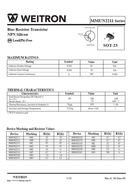
WEITRON
1/10
Rev.A 30-Dec-05
元器件交易网
MMUN2211 Series
ELECTRICAL CHARACTERISTICS (TA = 25 C unless otherwise noted)
Junction and Storage, Temperature
1. FR-4 @ minimun pad
Symbol
PD
R θJA TJ,Tstg
Value
246 1.6 625
-65 to +150
Unit
mW mW / ℃ ℃/W
℃
Device Marking and Resistor Values
Vin, INPUT VOLTAGE (VOL TS)
-
2. Pulse Test: Pulse Width < 300 ms, Duty Cycle < 2.0 %.
WEITRON
Typ Max Unit
-
100
nAdc
-
500
nAdc
-
mAdc 0.5
-
0.2
-
0.1
-
0.2
-
0.9
-
1.9
-
4.3
-
2.3
-
1.5
-
0.18
-
0.13
-
0.2
-
4.0
Characteristic
Symbol Min
OFF CHARACTERISTICS
Collector-Base Cutof f Current (VCB= 50 V, IE = 0)
十速 TM57PE11 8为单片机 说明书
Advance Informationtenx technology, inc.TM57PE118位 单片机使用手册Tenx reserves the right to change or discontinue this product without notice.tenx technology inc.CONTENTS1.基本功能 (2)2.系统结构图 (2)3.管脚分配图 (3)4.管脚描述 (3)5.功能描述 (4)5.1 CPU芯片 (4)5.1.1 时钟配置和指令周期 (4)5.1.2 寻址模式 (4)5.1.3 程序计数器和堆栈 (5)5.1.4 ALU和工作寄存器 (5)5.1.5 状态寄存器 (5)5.1.6 中断 (6)5.2 芯片工作模式 (7)5.2.1 复位 (7)5.2.2 系统配置寄存器(SYSCFG) (7)5.2.3 可重复编程 (8)5.2.4 省电模式 (8)5.3 外围功能图 (9)5.3.1 WDT/WKT定时器 (9)5.3.2 可扩展的8位定时计数器(定时器0)(PSC) (9)5.3.3 系统时钟振荡器 (10)5.4 I/O口 (11)5.4.1 PA0-1 (11)5.4.2 PA2-4 (12)5.4.3 PA7 (13)6.内存功能图 (13)F-Plane (13)R-Plane (14)7.指令表 (15)8.电气特性 (26)1 tenx technology, inc.2 tenx technology, inc.1. 基本功能1.ROM :1K ⅹ14 OTP 或者512ⅹ14位 TTP TM (ROM 可编程两次) 2.PAM :48ⅹ8位 3. 堆栈:5级4. I/O 口:可编程三次(最大6脚)5. 定时计数器:带有1-256预分频的8位定时控制器6. 看门狗/唤醒定时器:基于内部RC 振荡,唤醒时间为20-160毫秒的芯片定时器7. 复位:电源复位,看门狗复位,低电压复位,外部复位8. 系统时钟模式:- 内部RC :4MHZ - 外部RC 9. 工作电压:LV 复位电压至5.5V 10. 指令:36个11. 中断:两个管脚中断,定时器0中断和唤醒定时器中断 12. 支持省电模式2. 系统结构图3 tenx technology, inc.3. 管脚分配图VDD 1 U 8VSSXrc/PA4 2 7PA0/INT0 CLKO/PA33 TM57PE116PA1 VPP/INT2/nRESET/PA745PA2/T0I4. 管脚描述管脚名称输入/输出管脚描述PA0–PA1 I/O位编程I / O 端口,可施密特触发输入或CMOS 推挽输出或者伪开漏式输出。
G781中文资料

±1°C Remote and Local Temperature Sensor with SMBus Serial InterfaceFeaturesTwo Channels: Measures Both Remote andLocal Temperatures No Calibration RequiredSMBus 2-Wire Serial InterfaceProgrammable Under/Overtemperature Alarms Supports SMBus Alert Response Accuracy:±1°C (+60°C to +100°C, remote) ±3°C (+60°C to + 100°C, local)320µA (typ) Average Supply Current During Conversion+3V to +5.5V Supply Range Small 8-Lead SO PackageApplications Desktop and Notebook Central Office Computers Telecom Equipment Smart Battery Packs Test and Measurement LAN Servers Multi-Chip Modules Industrial Controllers General DescriptionThe G781 is a precise digital thermometer that reports the temperature of both a remote sensor and its own package. The remote sensor is a diode-connected transistor typically a low-cost, easily mounted 2N3904 NPN type that replace conventional thermistors or thermocouples. Remote accuracy is ±1°C with no cali-bration needed. The remote channel can also meas-ure the die temperature of other ICs, such as micro-processors, that contain an on-chip, diode-connected transistor.The 2-wire serial interface accepts standard System Management Bus (SMBus) Write Byte, Read Byte, Send Byte, and Receive Byte commands to program the alarm thresholds and to read temperature data.The data format is 11bits plus sign, with each bit cor-responding to 0.125°C, in two’s-complement format. Measurements can be done automatically and autonomously, with the conversion rate programmed by the user or programmed to operate in a single-shot mode. The adjustable rate allows the user to control the supply current drain.The G781 is available in a small, 8-pin SOP sur-face-mount package.Ordering InformationPART* TEMP. RANGE PIN-PACKAGEG781-20°C to +120°C8-SOPPin ConfigurationTypical Operating Circuit3V TO 5.5VEACHCLOCK DATAINTERRUPT TO µCSMBDATA SMBCLK GNDG781ALERTAbsolute Maximum RatingsVCC to GND………….….……..………….-0.3V to +6V DXP to GND……….……………..…-0.3V to VCC + 0.3V DXN to GND……………..……………..-0.3V to +0.8V SMBCLK, SMBDATA,ALERT to GND..…-0.3V to +6V SMBDATA,ALERT Current………….-1mA to +50mA DXN Current……………………..………………….±1mA ESD Protection (SMBCLK, SMBDATA,ALERT , humanbody model).……………………………………….2000V ESD Protection (other pins, human body model)..2000V Continuous Power Dissipation (T A = +70°C) ..SOP (derate 8.30mW/°C above +70°C)…………......667mW Operating Temperature Range………-20°C to +120°C Junction Temperature………………….………..+150°C Storage temperature Range………….-65°C to +165°C Lead Temperature (soldering, 10sec)……..……...+300°CStresses beyond those listed under “Absolute Maximum Ratings” may cause permanent damage to the device. These are stress ratings only, and functional operation of the device at these or any other conditions beyond those indicated in the opera-tional sections of the specifications is not implied. Exposure to absolute maximum rating conditions for extended periods may affect device reliability.Electrical Characteristics(VCC = + 3.3V, T A = 0°C to +85°C, unless otherwise noted.)PARAMETER CONDITIONS MIN TYP MAX UNITST R = +60°C to +100°C, VCC = 3.0V to 3.6V-1+1Temperature Error, Remote Di-ode (Note 1)T R = 0°C to +125°C (Note 2)-3 +3 °CT A = +60°C to +100°C-3 +3Temperature Error, Local DiodeT A = 0°C to +85°C (Note 2)-5 +5°CSupply-Voltage Range3.0 5.5 V Undervoltage Lockout Threshold VCC input, disables A/D conversion, rising edge 2.8 V Undervoltage Lockout Hysteresis 50 mV Power-On Reset Threshold VCC, falling edge 1.7 V POR Threshold Hysteresis 50 mVSMBus static3Standby Supply Current Logic inputs forced to VCC or GND Hardware or softwarestandby, SMBCLK at 10kHz4 µA0.5 conv/sec 35Average Operating Supply CurrentAuto-convert mode. Logic inputs forced to VCC or GND 8.0 conv/sec 320 µAConversion Time From stop bit to conversion complete (both channels) 125 ms Conversion Rate Timing Conversion-Rate Control Byte=04h, 1Hz 1 sec High level176Remote-Diode Source CurrentDXP forced to 1.5VLow level11µAElectrical Characteristics (continued)(VCC = + 3.3V, T A = 0 to +85°C, unless otherwise noted.)Note 1: A remote diode is any diode-connected transistor from Table1. T R is the junction temperature of the remote of the remote diode. See Remote Diode Selection for remote diode forward voltage requirements.Note 2: Guaranteed by design but not 100% tested.Pin DescriptionDetailed DescriptionThe G781 is a temperature sensor designed to work in conjunction with an external microcontroller (µC) or other intelligence in thermostatic, process-control, or monitoring applications. The µC is typically a power- management or keyboard controller, generating SMBus serial commands by “bit-banging” general- purpose input-output (GPIO) pins or via a dedicated SMBus interface block.Essentially an serial analog-to digital converter (ADC) with a sophisticated front end, the G781 contains a switched current source, a multiplexer, an ADC, an SMBus interface, and associated control logic (Figure 1). Temperature data from the ADC is loaded into two data registers, where it is automatically compared with data previously stored in several over/under- tem-perature alarm registers.ADC and MultiplexerThe ADC is an averaging type that integrates over a 60ms period (each channel, typical), with excellent noise rejection.The multiplexer automatically steers bias currents through the remote and local diodes, measures their forward voltages, and computes their temperatures. Both channels are automatically converted once the conversion process has started, either in free-running or single-shot mode. If one of the two channels is not used, the device still performs both measurements, and the user can simply ignore the results of the un-used channel. If the remote diode channel is unused, tie DXP to DXN rather than leaving the pins open. The worst-case DXP-DXN differential input voltage range is 0.25V to 0.95V.Excess resistance in series with the remote diode causes about +0.6°C error per ohm. Likewise, 240µV of offset voltage forced on DXP-DXN causes about 1°C error.Figure 1. Functional DiagramSMBDATA SMBCLKA/D Conversion SequenceIf a Start command is written (or generated automati-cally in the free-running auto-convert mode), both channels are converted, and the results of both meas-urements are available after the end of conversion. A BUSY status bit in the status byte shows that the de-vice is actually performing a new conversion; however, even if the ADC is busy, the results of the previous conversion are always available.Remote Diode SelectionTemperature accuracy depends on having a good- quality, diode-connected small-signal transistor. The G781 can also directly measure the die temperature of CPUs and other integrated circuits having on-board temperature-sensing diodes.The transistor must be a small-signal type with a rela-tively high forward voltage; otherwise, the A/D input voltage range can be violated. The forward voltage must be greater than 0.25V at 10µA; check to ensure this is true at the highest expected temperature. The forward voltage must be less than 0.95V at 300µA; check to ensure this is true at the lowest expected temperature. Large power transistors don’t work at all. Also, ensure that the base resistance is less than 100Ω. Tight specifications for forward-current gain (+50 to +150, for example) indicate that the manufac-turer has good process controls and that the devices have consistent V be characteristics.Thermal Mass and Self-HeatingThermal mass can seriously degrade the G781’s ef-fective accuracy. The thermal time constant of the SOP- package is about 140 in still air. For the G781 junction temperature to settle to within +1°C after a sudden +100°C change requires about five time con-stants or 12 minutes. The use of smaller packages for remote sensors, such as SOT23s, improves the situa-tion. Take care to account for thermal gradients be-tween the heat source and the sensor, and ensure that stray air currents across the sensor package do not interfere with measurement accuracy. Self-heating does not significantly affect measurement accuracy. Remote-sensor self-heating due to the diode current source is negligible. For the local diode, the worst-case error occurs when auto-converting at the fastest rate and simultaneously sinking maximum current at the ALERT output. For example, at an 8Hz rate and with ALERT sinking 1mA, the typical power dissipation isVCC x 320µA plus 0.4V x 1mA. Package theta J-A is about 120°C /W, so with VCC = 3.3V and no copper PC board heat-sinking, the resulting temperature rise is:dT =1.45mW x 120°C /W =0.17°CEven with these contrived circumstances, it is difficultto introduce significant self-heating errors.Table 1. Remote-Sensor Transistor Manufacturers MANUFACTURER MODELNUMBER Philips PMBS3904Motorola(USA) MMBT3904 National Semiconductor (USA) MMBT3904Note:Transistors must be diode-connected (baseshorted to collector).ADC Noise FilteringThe ADC is an integrating type with inherently good noise rejection. Micropower operation places con-straints on high-frequency noise rejection; therefore, careful PC board layout and proper external noise fil-tering are required for high-accuracy remote meas-urements in electrically noisy environments.High-frequency EMI is best filtered at DXP and DXNwith an external 2200pF capacitor. This value can be increased to about 3300pF(max), including cable ca-pacitance. Higher capacitance than 3300pF introduces errors due to the rise time of the switched current source.Nearly all noise sources tested cause the ADC meas-urements to be higher than the actual temperature, typically by +1°C to 10°C, depending on the frequencyand amplitude.PC Board LayoutPlace the G781 as close as practical to the remote diode. In a noisy environment, such as a computer motherboard, this distance can be 4 in. to 8 in. (typical)or more as long as the worst noise sources (such as CRTs, clock generators, memory buses, and ISA/PCI buses) are avoided.Do not route the DXP-DXN lines next to the deflection coils of a CRT. Also, do not route the traces across a fast memory bus, which can easily introduce +30°C error, even with good filtering, Otherwise, most noise sources are fairly benign.Route the DXP and DXN traces in parallel and in close proximity to each other, away from any high-voltage traces such as +12V DC. Leakage currents from PC board contamination must be dealt with carefully, since a 10MΩ leakage path from DXP to ground causes about +1°C error.Connect guard traces to GND on either side of the DXP-DXN traces (Figure 2). With guard traces in place, routing near high-voltage traces is no longer an issue.Route through as few vias and crossunders as possible to minimize copper/solder thermocouple ef-fects.When introducing a thermocouple, make sure that both the DXP and the DXN paths have matching thermocouples. In general, PC board-induced ther-mocouples are not a serious problem, A copper-solder thermocouple exhibits 3µV/°C, and it takes about 240µV of voltage error at DXP-DXN to cause a +1°C measurement error. So, most parasitic thermocouple errors are swamped out.Use wide traces. Narrow ones are more inductive and tend to pick up radiated noise. The 10 mil widths and spacing recommended on Figure 2 aren’t absolutely necessary (as they offer only a minor improvement in leakage and noise), but try to use them where practi-cal.Keep in mind that copper can’t be used as an EMI shield, and only ferrous materials such as steel work will. Placing a copper ground plane between the DXP-DXN traces and traces carrying high-frequency noise signals does not help reduce EMI.PC Board Layout ChecklistPlace the G781 close to a remote diode.Keep traces away from high voltages (+12V bus).Keep traces away from fast data buses and CRTs. Use recommended trace widths and spacing.Place a ground plane under the tracesUse guard traces flanking DXP and DXN and con necting to GND.Place the noise filter and the 0.1µF VCC bypass capacitors close to the G781.Figure 2. Recommended DXP/DXN PC Traces Twisted Pair and Shielded CablesFor remote-sensor distances longer than 8 in., or in particularly noisy environments, a twisted pair is rec-ommended. Its practical length is 6 feet to 12feet (typi cal) before noise becomes a problem, as tested in a noisy electronics laboratory. For longer distances, the best solution is a shielded twisted pair like that used for audio microphones. Connect the twisted pair to DXP and DXN and the shield to GND, and leave the shield’s remote end unterminated.Excess capacitance at DX_limits practical remote sen-sor distances (see Typical Operating Characteristics), For very long cable runs, the cable’s parasitic capaci-tance often provides noise filtering, so the 2200pF ca-pacitor can often be removed or reduced in value. Ca-ble resistance also affects remote-sensor accuracy; 1Ωseries resistance introduces about + 0.6°C error.Low-Power Standby ModeStandby mode disables the ADC and reduces the supply-current drain to about 10µA. Enter standby mode by forcing high to the RUN/STOP bit in the con-figuration byte register. Software standby mode be-haves such that all data is retained in memory, and the SMB interface is alive and listening for reads and writes.Software standby mode is not a shutdown mode. With activity on the SMBus, extra supply current is drawn (see Typical Operating Characteristics). In software standby mode, the G781 can be forced to perform A/D conversions via the one-shot command, despite the RUN/STOP bit being high.10 MILSMINIMUM10 MILS10 MILSIf software standby command is received while a con-version is in progress, the conversion cycle is trun-cated, and the data from that conversion is not latched into either temperature reading register. The previous data is not changed and remains available.Supply-current drain during the 125ms conversion period is always about 320µA. Slowing down the con-version rate reduces the average supply current (see Typical Operating Characteristics). In between con-versions, the instantaneous supply current is about 25µA due to the current consumed by the conversion rate timer. In standby mode, supply current drops to about 3µA. At very low supply voltages (under the power-on-reset threshold), the supply current is higher due to the address pin bias currents. It can be as high as 100µA, depending on ADD0 and ADD1 settings. SMBus Digital InterfaceFrom a software perspective, the G781 appears as a set of byte-wide registers that contain temperature data, alarm threshold values, or control bits, A stan-dard SMBus 2-wire serial interface is used to read temperature data and write control bits and alarm threshold data.Each A/D channel within the device responds to the same SMBus slave address for normal reads and writes.The G781 employs four standard SMBus protocols: Write Byte, Read Byte, Send Byte, and Receive Byte (Figure 3). The shorter Receive Byte protocol allows quicker transfers, provided that the correct data regis-ter was previously selected by a Read Byte instruction. Use caution with the shorter protocols in multi-master systems, since a second master could overwrite the command byte without informing the first master.The temperature data format is 11bits plus sign in twos-complement form for remote channel, with each data bit representing 0.125°C (Table 2,Table 3), transmitted MSB first. Table 2. Temperature Data Format(Two’s-Complement)DIGITAL OUTPUTDATA BITSTEMP.(°C)SIGN MSB LSB EXT+127.875 0 111 1111 111+126.375 0 111 1110 011+25.5 0 001 1001 100+1.75 0 000 0001 110+0.5 0 000 0000 100+0.125 0 000 0000 001-0.125 1 111 1111 111-1.125 1 111 1110 111-25.5 1 110 0110 100-55.25 1 100 1000 110-65.000 1 011 1111 000Table 3. Extended Temperature Data FormatEXTENDEDRESOLUTIONDATA BITS0.000°C 000000000.125°C 001000000.250°C 010000000.375°C 011000000.500°C 100000000.625°C 101000000.750°C 110000000.875°C 11100000Slave AddressThe G781 appears to the SMBus as one device hav-ing a common address for both ADC channels. The G781 device address is set to 1001100.The G781 also responds to the SMBus Alert Re-sponse slave address (see the Alert Response Ad-dress section).One-Shot RegisterThe One-shot register is to initiate a single conversion and comparison cycle when the device is in standby mode and auto conversion mode. The write operation to this register causes one-shot conversion and the data written to it is irrelevant and is not stored.Serial Bus Interface ReinitializationWhen SMBCLK are held low for more than 30ms (typical) during an SMBus communication the G781 will reinitiateits bus interface and be ready for a new transmission. Alarm Threshold RegistersFour registers store alarm threshold data, with high-temperature (T HIGH) and low-temperature (T LOW) registers for each A/D channel. If either measured temperature equals or exceeds the corresponding alarm threshold value, an ALERT interrupt is as-serted.The power-on-reset (POR) state of both T HIGH registers is full scale (01010101, or +85°C). The POR state of both T LOW registers is 0°C.Diode Fault AlarmThere is a fault detector at DXP that detects whether the remote diode has an open-circuit condition. At the beginning of each conversion, the diode fault is checked, and the status byte is updated. This fault de-tector is a simple voltage detector. If DXP rises above VCC – 1V (typical) due to the diode current source, a fault is detected and the device alarms through pulling ALERT low while the remote temperature reading doesn’t update in this condition. Note that the diode fault isn’t checked until a conversion is initiated, so im-mediately after power-on reset the status byte indicates no fault is present, even if the diode path is broken.If the remote channel is shorted (DXP to DXN or DXP to GND), the ADC reads 1000 0000(-128°C) so as not to trip either the T HIGH or T LOW alarms at their POR settings. ALERT InterruptsThe ALERT interrupt output signal is latched and canonly be cleared by reading the Alert Response ad-dress. Interrupts are generated in response to T HIGHand T LOW comparisons and when the remote diode is disconnected (for fault detection). The interrupt doesnot halt automatic conversions; new temperature datacontinues to be available over the SMBus interfaceafter ALERT is asserted. The interrupt output pin isopen-drain so that devices can share a common in-terrupt line. The interrupt rate can never exceed theconversion rate.The interface responds to the SMBus Alert Responseaddress, an interrupt pointer return-address feature(see Alert Response Address section). Prior to takingcorrective action, always check to ensure that an in-terrupt is valid by reading the current temperature.Alert Response AddressThe SMBus Alert Response interrupt pointer providesquick fault identification for simple slave devices thatlack the complex, expensive logic needed to be a busmaster. Upon receiving an ALERT interrupt signal,the host master can broadcast a Receive Byte trans-mission to the Alert Response slave address (0001100). Then any slave device that generated an inter-rupt attempts to identify itself by putting its own ad-dress on the bus (Table 4).The Alert Response can activate several differentslave devices simultaneously, similar to the SMBusGeneral Call. If more than one slave attempts to re-spond, bus arbitration rules apply, and the device withthe lower address code wins. The losing device doesnot generate an acknowledge and continues to holdthe ALERT line low until serviced (implies that thehost interrupt input is level-sensitive). Successfulreading of the alert response address clears the inter-rupt latch.Table 4. Read Format for Alert Response Address(0001 100)BIT NAME7(MSB) ADD76 ADD65 ADD54 ADD43 ADD32 ADD21 ADD10(LSB) 1Command Byte FunctionsThe 8-bit command byte register (Table 5) is the mas-ter index that points to the various other registers within the G781. The register’s POR state is 0000 0000, so that a Receive Byte transmission (a protocol that lacks the command byte) that occurs immediately after POR returns the current local temperature data.The one-shot command immediately forces a new conversion cycle to begin. In software standby mode (RUN/STOP bit = high), a new conversion is begun, after which the device returns to standby mode. If a conversion is in progress when a one-shot command is received in auto-convert mode (RUN/STOP bit = low) between conversions, a new conversion begins, the conversion rate timer is reset, and the next auto-matic conversion takes place after a full delay elapses.Configuration Byte FunctionsThe configuration byte register (Table 6) is used to mask interrupts and to put the device in software standby mode. The other bits are empty. Status Byte FunctionsThe status byte register (Table 7) indicates which (if any) temperature thresholds have been exceeded. This byte also indicates whether or not the ADC is converting and whether there is an open circuit in the remote diode DXP-DXN path. After POR, the normal state of all the flag bits is zero, assuming none of the alarm conditions are present. The status byte is cleared by any successful read of the status, unless the fault persists. Note that the ALERT interrupt latch is not automatically cleared when the status flag bit is cleared.When reading the status byte, you must check for in-ternal bus collisions caused by asynchronous ADC timing, or else disable the ADC prior to reading the status byte (via the RUN/STOP bit in the configura-tion byte). In one-shot mode, read the status byte only after the conversion is complete, which is approxi-mately 125ms max after the one-shot conversion is commanded.Table 5. Command-Byte Bit Assignments*If the device is in standby mode at POR, both temperature registers read 0°C.Table 6. Configuration-Byte Bit AssignmentsTable 7. Status-Byte Bit Assignments*These flags stay high until cleared by POR, or until the status byte register is read.Table 8. Conversion-Rate Control ByteDATA CONVERSION RATE (Hz)00h 0.062501h 0.12502h 0.2503h 0.504h 105h 206h 407h 808h 16 09h to FFh RFUTo check for internal bus collisions, read the status byte. If the least significant seven bits are ones, dis-card the data and read the status byte again. The status bits LHIGH, LLOW, RHIGH, and RLOW are refreshed on the SMBus clock edge immediately fol-lowing the stop condition, so there is no danger of los-ing temperature-related status data as a result of an internal bus collision. The OPEN status bit (diode con-tinuity fault) is only refreshed at the beginning of a conversion, so OPEN data is lost. The ALERT inter-rupt latch is independent of the status byte register, so no false alerts are generated by an internal bus colli-sion. When auto-converting, if the THIGH and TLOW limits are close together, it’s possible for both high-temp and low-temp status bits to be set, depending on the amount of time between status read operations (espe-cially when converting at the fastest rate). In these circumstances, it’s best not to rely on the status bits to indicate reversals in long-term temperature changes and instead use a current temperature reading to es-tablish the trend direction.For bit 1 and bit 0, a high indicates a temperature alarm happened for remote and local diode respec-tively. THERM pin also asserts. These two bits wouldn’t be cleared when reading status byte.Conversion Rate ByteThe conversion rate register (Table 8) programs the time interval between conversions in free-running auto-convert mode. This variable rate control reduces the supply current in portable-equipment applications. The conversion rate byte’s POR state is 08h (16Hz). The G781 looks only at the 4 LSB bits of this register, so the upper 4 bits are “don’t care” bits, which should be set to zero. The conversion rate tolerance is ±25% at any rate setting.Valid A/D conversion results for both channels are available one total conversion time (125ms,typical) after initiating a conversion, whether conversion is initiated via the RUN/STOP bit, one-shot command, or initial power-up.POR AND UVLOThe G781 has a volatile memory. To prevent ambiguous power-supply conditions from corrupting the data in memory and causing erratic behavior, a POR voltage detector monitors VCC and clears the memory if VCC falls below 1.7V (typical, see Electrical Characteristics table). When power is first applied and VCC rises above 1.7V (typical), the logic blocks begin operating, although reads and writes at V CC levels below 3V are not recom-mended. A second VCC comparator, the ADC UVLO comparator, prevents the ADC from converting until there is sufficient headroom (VCC= 2.8V typical).ALERT Fault QueueTo suppress unwanted ALERT triggering the G781 em-bedded a fault queue function. The ALERT won’t as-sert until consecutive out of limit measurements have reached the queue number. The mapping of fault queue register (ALERTFQ, 22h) value to fault queue number is shown in the Table 9.Table 9. Alert Fault QueueALERTFQVALUEFAULT QUEUE NUMBER XXXX000X 1XXXX001X 2XXXX010X 3XXXX011X 3XXXX100X 4XXXX101X 4XXXX110X 4XXXX111X 4 Operation of The THERM FunctionA local and remote THERM limit can be programmed into the G781 to set the temperature limit above which the THERM pin asserts low and the bit 1, of status byte will be set to 1 corresponding to remote and local over temperature. These two bits won’t be cleared to 0 by reading status byte it the over temperature condi-tion remain. A hysteresis value is provided by writing the register 21h to set the temperature threshold to release the THERM pin alarm state, The releasing temperature is the value of register 19h, 20h minus the value in register 21h. The format of register 21h is 2’s complement. The THERM signal is open drain and requires a pull-up resistor to power supply.Figure 4. SMBus Write Timing DiagramA = start condition H = LSB of data clocked into slaveB = MSB of address clocked into slave I = slave pulls SMBDATA line lowC = LSB of address clocked into slave J = acknowledge clocked into masterD = R/W bit clocked into slave K = acknowledge clocked pulseE = slave pulls SMBDATA line low L = stop condition data executed by slaveF = acknowledge bit clocked into master M = new start conditionG = MSB of data clocked into slaveFigure 5. SMBus Read Timing DiagramA = start condition G = MSB of data clocked into masterB = MSB of address clocked into slave H = LSB of data clocked into masterC = LSB of address clocked into slave I = acknowledge clocked pulseD = R/W bit clocked into slave J = stop conditionE = slave pulls SMBDATA line low K= new start conditionF =acknowledge bit clocked into master。
货代常用术语缩写
船务术语简缩语:主要贸易术语:(1) FCA (Free Carrier) 货交承运人(2) FAS (Free Alongside Ship) 装运港船边交货(3) FOB (Free on Board) 装运港船上交货(4) CFR (Cost and Freight) 成本加运费(5) CIF (Cost,Insurance and Freight) 成本、保险费加运费(6) CPT (Carriage Paid To) 运费付至目的地(7) CIP (Carriage and Insurance Paid To) 运费、保险费付至目的地(8) DAF (Delivered At Frontier) 边境交货(9) DES (Delivered Ex Ship) 目的港船上交货(10) DEQ (Delivered Ex Quay) 目的港码头交货(11) DDU (Delivered Duty Unpaid) 未完税交货(12) DDP (Delivered Duty Paid) 完税后交货主要船务术语简写:(1) ORC (Origin Recevie Charges) 本地收货费用( 广东省收取)(2) THC (Terminal Handling Charges) 码头操作费( 香港收取)(3) BAF (Bunker Adjustment Factor) 燃油附加费(4) CAF (Currency Adjustment Factor) 货币贬值附加费(5) YAS (Yard Surcharges) 码头附加费(6) EPS (Equipment Position Surcharges) 设备位置附加费(7) DDC (Destination Delivery Charges) 目的港交货费(8) PSS (Peak Season Sucharges) 旺季附加费(9) PCS (Port Congestion Surcharge) 港口拥挤附加费(10) DOC (DOcument charges) 文件费(11) O/F (Ocean Freight) 海运费(12) B/L (Bill of Lading) 海运提单(13) MB/L(Master Bill of Lading) 船东单(14) MTD (Multimodal Transport Document) 多式联运单据(15) L/C (Letter of Credit) 信用证(16) C/O (Certificate of Origin) 产地证(17) S/C (Sales Confirmation) 销售确认书( Sales Contract) 销售合同(18) S/O (Shipping Order) 装货指示书(19) W/T (Weight Ton) 重量吨( 即货物收费以重量计费)(20) M/T (Measurement Ton) 尺码吨( 即货物收费以尺码计费)(21) W/M(Weight or Measurement ton) 即以重量吨或者尺码吨中从高收费(22) CY (Container Yard) 集装箱(货柜)堆场(23) FCL (Full Container Load) 整箱货(24) LCL (Less than Container Load) 拼箱货( 散货)(25) CFS (Container Freight Station) 集装箱货运站(26) TEU (Twenty-feet Equivalent Units) 20 英尺换算单位( 用来计算货柜量的多少)(27) A/W (All Water) 全水路(主要指由美国西岸中转至东岸或内陆点的货物的运输方式)(28) MLB(Mini Land Bridge) 迷你大陆桥(主要指由美国西岸中转至东岸或内陆点的货物的运输方式)(29) NVOCC(No n-Vessel Operat ing Com mon Carrier) 无船承运人中外船公司简称与缩写一览公司澳大利亚国家航运公司美国总统轮船私人有限公司邦拿美船务有限公司波罗的海航运公司中波轮船股份公司南美邮船公司南美智利国家航运公司中日国际轮渡有限公司天敬海运法国达飞轮船公司京汉海运有限公司中国远洋集装箱运输有限公司朝阳商船有限公司达贸国际轮船公司德国胜利航运公司埃及国际轮船公司长荣海运股份有限公司远东轮船公司金发船务有限公司浩洲船务公司韩进海运有限公司香港航运有限公司香港明华船务有限公司赫伯罗特船务有限公司现代商船有限公司上海海隆轮船有限公司金华航运有限公司川崎汽船株式会社高丽海运株氏会社七星轮船有限公司上海育海航运公司上海中福轮船公司墨西哥航运有限公司上海天海货运有限公司东航船务有限公司阿拉伯联合国家轮船公司立荣海运股份有限公司环球船务有限公司万海航运股份有限公司阳明海运股份有限公司简称澳国航运美国总统邦拿美波罗的海中波南美邮船智利航运中日轮渡天敬海运达飞轮船京汉海运中远集运朝阳商船达贸国际德国胜利埃及船务长荣海运远东轮船金发船务浩洲船务韩进海运香港海运香港明华赫伯罗特现代商船海隆轮船金华航运川崎汽船咼丽海运七星轮船育海航运中福轮船墨西哥航运天海货运东航船务阿拉伯轮船立荣海运环球船务万海航运阳明海运缩写ANLAPLBNMLBOLC-PCLAN S.ACCNICHINJIFCKCMACO-HEUNGCOSCOCHOYANGDELIMASSENATOREILEVERGREENFESCOGFNGHCSCHANJINHKMSHHKMWHAPPAG-LLOYDHY UNDAI(HMM)HNTJHKLINEKMTCSSCLSYHSZFSCTMMTMSCTOHOUASCUNIGLORYUNIWD以星轮船船务有限公司联丰船务有限公司意大利邮船公司以星轮船联丰船务意大利邮船ZIMLIFENLT马来西亚国际航运有限公司马来西亚航运MISC商船一井有限公司商船二井MOL 地中海航运公司地中海航运MSC马士基海陆有限公司马士基海陆MAERSK -SEALAND民生神原海运有限公司民生神原SKM铁行渣华船务有限公司铁行渣华P&O NEDLLO YD 北欧亚航运有限公司北欧亚航运NORASIA沙特阿拉伯国家航运公司沙特航运NSCSA日本邮船有限公司日本邮船NYK东方海外货柜航运有限公司东方海外OOCL萨姆达拉船务有限公司萨姆达拉SAMUDERA太平船务有限公司太平船务PIL瑞克麦斯轮船公司瑞克麦斯RICKMERS南非国家轮船有限公司南非轮船SAF长锦有限公司长锦公司SINKO上海市锦江航运有限公司锦江船代JINJIANG中外运(集团)总公司中外运SINOTRANS装运英汉互译1. The shipme nt has arrived in good con diti on.运到之货情况良好。
MEMORY存储芯片ADM708ARZ-REEL中文规格书

Data SheetADuM1410/ADuM1411/ADuM1412FEATURESLow power operation 5 V operation1.3 mA per channel maximum at 0 Mbps to 2 Mbps 4.0 mA per channel maximum at 10 Mbps 3 V operation0.8 mA per channel maximum at 0 Mbps to 2 Mbps 1.8 mA per channel maximum at 10 Mbps Bidirectional communication 3 V/5 V level translationHigh temperature operation: 105°C Up to 10 Mbps data rate (NRZ)Programmable default output stateHigh common-mode transient immunity: >25 kV/µs 16-lead, RoHS compliant, SOIC wide body package Safety and regulatory approvalsUL recognition: 3750 V rms for 1 minute per UL 1577 CSA Component Acceptance Notice 5A VDE certificate of conformityDIN V VDE V 0884-10 (VDE V 0884-10): 2006-12 V IORM = 560 V peakTÜV approval: IEC/EN 60950-1V GND V V V V GND DD22OA OB OC OD2206580-001Figure 1. ADuM1410V GND V V V V CTRL GND DD22OA OB OC ID2206580-002Figure 2. ADuM1411V GND V V V V CTRL GNDDD22OA OB IC ID 2206580-003APPLICATIONSGeneral-purpose multichannel isolation SPI interface/data converter isolation RS-232/RS-422/RS-485 transceivers Industrial field bus isolationGENERAL DESCRIPTIONThe ADuM1410/ADuM1411/ADuM14121 are four-channel digital isolators based on Analog Devices, Inc., i Coupler® technology. Combining high speed CMOS and monolithic air core transformer technologies, these isolation components provide outstanding performance characteristics superior to alternatives such as optocoupler devices.By avoiding the use of LEDs and photodiodes, i Coupler devices remove the design difficulties commonly associated with opto-couplers. The usual concerns that arise with optocouplers, such as uncertain current transfer ratios, nonlinear transfer functions, and temperature and lifetime effects, are eliminated with the simple i Coupler digital interfaces and stable performance characteristics. The need for external drivers and other discrete components is eliminated with these i Coupler products. Furthermore, i Coupler1Protected by U.S. Patents 5,952,849; 6,873,065; 6,903,578; and 7,075,329.Figure 3. ADuM1412devices consume one-tenth to one-sixth the power of optocou-plers at comparable signal data rates.The ADuM1410/ADuM1411/ADuM1412 isolators provide four independent isolation channels in a variety of channel configu-rations and data rates (see the Ordering Guide) up to 10 Mbps. All models operate with the supply voltage on either side ranging from 2.7 V to 5.5 V , providing compatibility with lower voltage systems as well as enabling voltage translation functionality across the isolation barrier. All products also have a default output control pin. This allows the user to define the logic state the outputs are to adopt in the absence of the input power. Unlike other optocoupler alternatives, the ADuM1410/ADuM1411/ ADuM1412 isolators have a patented refresh feature that ensures dc correctness in the absence of input logic transitions and during power-up/power-down conditions.Data Sheet ADuM1410/ADuM1411/ADuM1412 SPECIFICATIONSELECTRICAL CHARACTERISTICS—5 V OPERATION4.5 V ≤ V DD1 ≤5.5 V, 4.5 V ≤ V DD2 ≤ 5.5 V; all minimum/maximum specifications apply over the entire recommended operation range, unless otherwise noted; all typical specifications are at T A = 25°C, V DD1 = V DD2 = 5 V. All voltages are relative to their respective ground. Table 1.Parameter Symbol Min Typ Max Unit Test Conditions/CommentsDC SPECIFICATIONSInput Supply Current per Channel,QuiescentI DDI (Q)0.50 0.73 mAOutput Supply Current per Channel,QuiescentI DDO (Q)0.38 0.53 mAADuM1410, Total Supply Current,Four Channels1DC to 2 MbpsV DD1 Supply Current I DD1 (Q) 2.4 3.2 mA DC to 1 MHz logic signal frequency V DD2 Supply Current I DD2 (Q) 1.2 1.6 mA DC to 1 MHz logic signal frequency10 Mbps (BRWZ Version Only)V DD1 Supply Current I DD1 (10)8.8 12 mA 5 MHz logic signal frequency V DD2 Supply Current I DD2 (10) 2.8 4.0 mA 5 MHz logic signal frequency ADuM1411, Total Supply Current,Four Channels1DC to 2 MbpsV DD1 Supply Current I DD1 (Q) 2.2 2.8 mA DC to 1 MHz logic signal frequency V DD2 Supply Current I DD2 (Q) 1.8 2.4 mA DC to 1 MHz logic signal frequency10 Mbps (BRWZ Version Only)V DD1 Supply Current I DD1 (10) 5.4 7.6 mA 5 MHz logic signal frequency V DD2 Supply Current I DD2 (10) 3.8 5.3 mA 5 MHz logic signal frequency ADuM1412, Total Supply Current,Four Channels1DC to 2 MbpsV DD1 or V DD2 Supply Current I DD1 (Q), I DD2(Q)2.0 2.6 mA DC to 1 MHz logic signal frequency10 Mbps (BRWZ Version Only)V DD1 or V DD2 Supply Current I DD1 (10), I DD2 (10) 4.6 6.5 mA 5 MHz logic signal frequencyAll ModelsInput Currents I IA, I IB, I IC,I ID, I CTRL1,I CTRL2, I DISABLE −10 +0.01 +10µA 0 V ≤ V IA, V IB, V IC, V ID ≤ V DD1 or V DD2,0 V ≤ V CTRL1, V CTRL2 ≤ V DD1 or V DD2,0 V ≤ V DISABLE ≤ V DD1Logic High Input Threshold V IH 2.0 V Logic Low Input Threshold V IL 0.8 VLogic High Output Voltages V OAH, V OBH,V OCH, V ODH (V DD1 or V DD2) − 0.1 5.0 V I Ox = −20 µA, V Ix = V IxH (V DD1 or V DD2) − 0.4 4.8 V I Ox = −4 mA, V Ix = V IxHLogic Low Output Voltages V OAL, V OBL,V OCL, V ODL0.0 0.1 V I Ox = 20 µA, V Ix = V IxL0.04 0.1 V I Ox = 400 µA, V Ix = V IxL0.2 0.4 V I Ox = 4 mA, V Ix = V IxL Rev. M | Page of 22ADuM1410/ADuM1411/ADuM1412 Data Sheet Parameter Symbol Min Typ Max Unit Test Conditions/Comments SWITCHING SPECIFICATIONSADuM1410ARWZ/ADuM1411ARWZ/ADuM1412ARWZMinimum Pulse Width2PW 1000 ns C L = 15 pF, CMOS signal levels Maximum Data Rate3 1 Mbps C L = 15 pF, CMOS signal levels Propagation Delay4t PHL, t PLH20 65 100 ns C L = 15 pF, CMOS signal levels Pulse Width Distortion, |t PLH − t PHL|4 PWD 40 ns C L = 15 pF, CMOS signal levels Propagation Delay Skew5t PSK50 ns C L = 15 pF, CMOS signal levels Channel-to-Channel Matching6t PSKCD/OD50 ns C L = 15 pF, CMOS signal levels ADuM1410BRWZ/ADuM1411BRWZ/ADuM1412BRWZMinimum Pulse Width2PW 100 ns C L = 15 pF, CMOS signal levels Maximum Data Rate310 Mbps C L = 15 pF, CMOS signal levels Propagation Delay4t PHL, t PLH20 30 50 ns C L = 15 pF, CMOS signal levels Pulse Width Distortion, |t PLH − t PHL|4 PWD 5 ns C L = 15 pF, CMOS signal levels Change vs. Temperature 5 ps/°C C L = 15 pF, CMOS signal levels Propagation Delay Skew5t PSK30 ns C L = 15 pF, CMOS signal levels Channel-to-Channel Matching,Codirectional Channels6t PSKCD 5 ns C L = 15 pF, CMOS signal levelsChannel-to-Channel Matching,Opposing-Directional Channels6t PSKOD 6 ns C L = 15 pF, CMOS signal levelsAll ModelsOutput Rise/Fall Time (10% to 90%) t R/t F 2.5 ns C L = 15 pF, CMOS signal levelsCommon-Mode Transient Immunity at Logic High Output7|CM H| 25 35 kV/µs V Ix = V DD1 or V DD2, V CM = 1000 V,transient magnitude = 800 VCommon-Mode Transient Immunity at Logic Low Output7 |CM L| 25 35 kV/µs V Ix = 0 V, V CM = 1000 V,transient magnitude = 800 VRefresh Rate f r 1.2 MbpsInput Enable Time8t ENABLE 2.0 µs V IA, V IB, V IC, V ID = 0 V or V DD1 Input Disable Time8t DISABLE 5.0 µs V IA, V IB, V IC, V ID = 0 V or V DD1Input Dynamic Supply Current per Channel9I DDI (D)0.12 mA/MbpsOutput Dynamic Supply Current per Channel9I DDO (D)0.04 mA/Mbps1 The supply current values for all four channels are combined when running at identical data rates. Output supply current values are specified with no output load present. The supply current associated with an individual channel operating at a given data rate can be calculated as described in the Power Consumption section. See Figure 8 through Figure 10 for information on per-channel supply current as a function of data rate for unloaded and loaded conditions. See Figure 11 through Figure 15 for total V DD1 and V DD2 supply currents as a function of data rate for ADuM1410/ADuM1411/ADuM1412 channel configurations.2 The minimum pulse width is the shortest pulse width at which the specified pulse width distortion is guaranteed.3 The maximum data rate is the fastest data rate at which the specified pulse width distortion is guaranteed.4 t PHL propagation delay is measured from the 50% level of the falling edge of the V Ix signal to the 50% level of the falling edge of the V Ox signal. t PLH propagation delay is measured from the 50% level of the rising edge of the V Ix signal to the 50% level of the rising edge of the V Ox signal.5 t PSK is the magnitude of the worst-case difference in t PHL or t PLH that is measured between units at the same operating temperature, supply voltages, and output load within the recommended operating conditions.6 Codirectional channel-to-channel matching is the absolute value of the difference in propagation delays between any two channels with inputs on the same side of the isolation barrier. Opposing-directional channel-to-channel matching is the absolute value of the difference in propagation delays between any two channels with inputs on opposing sides of the isolation barrier.7 |CM H| is the maximum common-mode voltage slew rate that can be sustained while maintaining V O > 0.8 V DD2. |CM L| is the maximum common-mode voltage slew rate that can be sustained while maintaining V O < 0.8 V. The common-mode voltage slew rates apply to both rising and falling common-mode voltage edges. The transient magnitude is the range over which the common mode is slewed.8 Input enable time is the duration from when V DISABLE is set low until the output states are guaranteed to match the input states in the absence of any input data logic transitions. If an input data logic transition within a given channel does occur within this time interval, the output of that channel reaches the correct state within the much shorter duration as determined by the propagation delay specifications within this data sheet. Input disable time is the duration from when V DISABLE is set high until the output states are guaranteed to reach their programmed output levels, as determined by the CTRL2 logic state (see Table 14).9 Dynamic supply current is the incremental amount of supply current required for a 1 Mbps increase in signal data rate. See Figure 8 through Figure 10 for information on per-channel supply current for unloaded and loaded conditions. See the Power Consumption section for guidance on calculating the per-channel supply current for a given data rate.Rev. M | Page of 22Data Sheet ADuM1410/ADuM1411/ADuM1412ELECTRICAL CHARACTERISTICS—3 V OPERATION2.7 V ≤ V DD1 ≤3.6 V, 2.7 V ≤ V DD2 ≤ 3.6 V; all minimum/maximum specifications apply over the entire recommended operation range, unless otherwise noted; all typical specifications are at T A = 25°C, V DD1 = V DD2 = 3.0 V. All voltages are relative to their respective ground. Table 2.Parameter Symbol Min Typ Max Unit Test Conditions/CommentsDC SPECIFICATIONSInput Supply Current per Channel,QuiescentI DDI (Q)0.25 0.38 mAOutput Supply Current per Channel,QuiescentI DDO (Q)0.19 0.33 mAADuM1410, Total Supply Current,Four Channels1DC to 2 MbpsV DD1 Supply Current I DD1 (Q) 1.2 1.6 mA DC to 1 MHz logic signalfrequency V DD2 Supply Current I DD2 (Q)0.8 1.0 mA DC to 1 MHz logic signalfrequency10 Mbps (BRWZ Version Only)V DD1 Supply Current I DD1 (10) 4.5 6.5 mA 5 MHz logic signal frequency V DD2 Supply Current I DD2 (10) 1.4 1.8 mA 5 MHz logic signal frequency ADuM1411, Total Supply Current,Four Channels1DC to 2 MbpsV DD1 Supply Current I DD1 (Q) 1.0 1.9 mA DC to 1 MHz logic signal frequency V DD2 Supply Current I DD2 (Q)0.9 1.7 mA DC to 1 MHz logic signal frequency10 Mbps (BRWZ Version Only)V DD1 Supply Current I DD1 (10) 3.1 4.5 mA 5 MHz logic signal frequency V DD2 Supply Current I DD2 (10) 2.1 3.0 mA 5 MHz logic signal frequency ADuM1412, Total Supply Current,Four Channels1DC to 2 MbpsV DD1 or V DD2 Supply Current I DD1 (Q), I DD2 (Q) 1.0 1.8 mA DC to 1 MHz logic signal frequency10 Mbps (BRWZ Version Only)V DD1 or V DD2 Supply Current I DD1 (10), I DD2 (10) 2.6 3.8 mA 5 MHz logic signal frequencyAll ModelsInput Currents I IA, I IB, I IC, I ID,I CTRL1,I CTRL2, I DISABLE −10 +0.01 +10µA 0 V ≤ V IA, V IB, V IC, V ID ≤ V DD1 or V DD2,0 V ≤ V CTRL1, V CTRL2 ≤ V DD1 or V DD2,0 V ≤ V DISABLE ≤ V DD1Logic High Input Threshold V IH 1.6 V Logic Low Input Threshold V IL 0.4 VLogic High Output Voltages V OAH, V OBH,V OCH, V ODH (V DD1 or V DD2) − 0.1 3.0 V I Ox = −20 µA, V Ix = V IxH (V DD1 or V DD2) − 0.4 2.8 V I Ox = −4 mA, V Ix = V IxHLogic Low Output Voltages V OAL, V OBL,V OCL, V ODL0.0 0.1 V I Ox = 20 µA, V Ix = V IxL0.04 0.1 V I Ox = 400 µA, V Ix = V IxL0.2 0.4 V I Ox = 4 mA, V Ix = V IxL Rev. M | Page of 22ADuM1410/ADuM1411/ADuM1412 Data Sheet。
MMSZ11T3资料
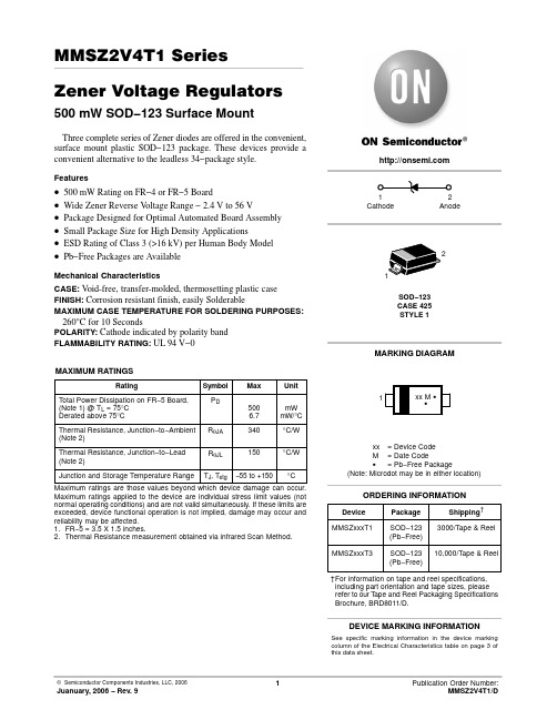
MMSZ2V4T1 SeriesZener Voltage Regulators 500 mW SOD−123 Surface MountThree complete series of Zener diodes are offered in the convenient, surface mount plastic SOD−123 package. These devices provide a convenient alternative to the leadless 34−package style.Features•500 mW Rating on FR−4 or FR−5 Board•Wide Zener Reverse V oltage Range − 2.4 V to 56 V •Package Designed for Optimal Automated Board Assembly •Small Package Size for High Density Applications•ESD Rating of Class 3 (>16 kV) per Human Body Model •Pb−Free Packages are AvailableMechanical CharacteristicsCASE:V oid-free, transfer-molded, thermosetting plastic case FINISH:Corrosion resistant finish, easily SolderableMAXIMUM CASE TEMPERATURE FOR SOLDERING PURPOSES: 260°C for 10 SecondsPOLARITY:Cathode indicated by polarity band FLAMMABILITY RATING:UL 94 V−0MAXIMUM RATINGSRating Symbol Max UnitTotal Power Dissipation on FR−5 Board, (Note 1) @ T L = 75°CDerated above 75°C P D5006.7mWmW/°CThermal Resistance, Junction−to−Ambient(Note 2)R q JA340°C/WThermal Resistance, Junction−to−Lead(Note 2)R q JL150°C/W Junction and Storage Temperature Range T J, T stg−55 to +150°C Maximum ratings are those values beyond which device damage can occur. Maximum ratings applied to the device are individual stress limit values (notnormal operating conditions) and are not valid simultaneously. If these limits are exceeded, device functional operation is not implied, damage may occur and reliability may be affected.1.FR−5 = 3.5 X 1.5 inches.2.Thermal Resistance measurement obtained via infrared Scan Method.Device Package Shipping†ORDERING INFORMATIONSee specific marking information in the device marking column of the Electrical Characteristics table on page 3 of this data sheet.DEVICE MARKING INFORMATION†For information on tape and reel specifications, including part orientation and tape sizes, please refer to our T ape and Reel Packaging Specifications Brochure, BRD8011/D.MMSZxxxT1SOD−123(Pb−Free)3000/Tape & ReelMMSZxxxT3SOD−123(Pb−Free)10,000/Tape & ReelELECTRICAL CHARACTERISTICS (T A = 25°C unless otherwise noted, V F = 0.95 V Max. @ I F = 10 mA)Symbol ParameterV Z Reverse Zener Voltage @ I ZTI ZTReverse CurrentZ ZT Maximum Zener Impedance @ I ZT I R Reverse Leakage Current @ V R V R Reverse VoltageI F Forward CurrentV F Forward Voltage @ I FDevice†DeviceMarking(Notes 3 and 4)(Note 5)(Notes 3 and 4)(Note 5)Leakage Current @ I ZT1 = 5 mA@ I ZT2 = 1 mA I R @ V R Min Nom Max W Min Max W m A VoltsMMSZ2V4T1T1 2.28 2.4 2.52100 1.7 2.1600501 MMSZ2V7T1T2 2.57 2.7 2.84100 1.9 2.4600201 MMSZ3V0T1*T3 2.85 3.0 3.1595 2.1 2.7600101 MMSZ3V3T1T4 3.14 3.3 3.4795 2.3 2.960051 MMSZ3V6T1T5 3.42 3.6 3.7890 2.7 3.360051 MMSZ3V9T1U1 3.71 3.9 4.1090 2.9 3.560031 MMSZ4V3T1U2 4.09 4.3 4.5290 3.3 4.060031 MMSZ4V7T1U3 4.47 4.7 4.9480 3.7 4.750032 MMSZ5V1T1U4 4.85 5.1 5.3660 4.2 5.348022 MMSZ5V6T1*U5 5.32 5.6 5.8840 4.8 6.040012 MMSZ6V2T1*V1 5.89 6.2 6.5110 5.6 6.615034 MMSZ6V8T1V2 6.46 6.87.1415 6.37.28024 MMSZ7V5T1V37.137.57.8815 6.97.98015 MMSZ8V2T1V47.798.28.61157.68.7800.75 MMSZ9V1T1V58.659.19.56158.49.61000.56 MMSZ10T1A19.501010.50209.310.61500.27 MMSZ11T1A210.451111.552010.211.61500.18 MMSZ12T1A311.401212.602511.212.71500.18 MMSZ13T1A412.351313.653012.314.01700.18 MMSZ15T1A514.251515.753013.715.52000.0510.5 MMSZ16T1X115.201616.804015.217.02000.0511.2 MMSZ18T1X217.101818.904516.719.02250.0512.6 MMSZ20T1X319.002021.005518.721.12250.0514 MMSZ22T1X420.902223.105520.723.22500.0515.4 MMSZ24T1X522.802425.207022.725.52500.0516.83.The type numbers shown have a standard tolerance of ±5% on the nominal Zener Voltage.4.Tolerance and Voltage Designation: Zener Voltage (V Z) is measured with the Zener Current applied for PW = 1 ms.5.Z ZT and Z ZK are measured by dividing the AC voltage drop across the device by the AC current applied.The specified limits are for I Z(AC)= 0.1 I Z(DC),with the AC frequency = 1 kHz.†The “G” suffix indicates Pb−Free package available.*Not Available in the 10,000/Tape & Reel.Device†DeviceMarking(Notes 6 and 7)(Note 8)(Notes 6 and 7)(Note 8)Leakage Current @ I ZT1 = 2 mA@ I ZT2 = 0.1 mA@ I ZT2 =0.5 mA I R @ V RMin Nom Max W Min Max W m A VoltsMMSZ27T1Y125.652728.35802528.93000.0518.9 MMSZ30T1*Y228.503031.508027.8323000.0521 MMSZ33T1Y331.353334.658030.8353250.0523.1 MMSZ36T1*Y434.203637.809033.8383500.0525.2 MMSZ39T1*Y537.053940.9513036.7413500.0527.3 MMSZ43T1*Z140.854345.1515039.7463750.0530.1 MMSZ47T1Z244.654749.3517043.7503750.0532.9 MMSZ51T1*Z348.455153.5518047.6544000.0535.7 MMSZ56T1Z453.205658.8020051.5604250.0539.26.The type numbers shown have a standard tolerance of ±5% on the nominal Zener Voltage.7.Tolerance and Voltage Designation: Zener Voltage (V Z) is measured with the Zener Current applied for PW = 1 ms.8.Z ZT and Z ZK are measured by dividing the AC voltage drop across the device by the AC current applied.The specified limits are for I Z(AC)= 0.1 I Z(DC),with the AC frequency = 1 kHz.†The “G” suffix indicates Pb−Free package available.*Not Available in the 10,000/Tape & Reel.V Z , T E M P E R A T U R E C O E F F I C I E N T (m V /C )°θV Z , NOMINAL ZENER VOLTAGE (V)−−−1012345678Figure 1. Temperature Coefficients (Temperature Range −55°C to +150°C)V Z , T E M P E R A T U R E C O E F F I C I E N T (m V /C )°θ100101V Z, NOMINAL ZENER VOLTAGE (V)Figure 2. Temperature Coefficients (Temperature Range −55°C to +150°C)1.21.00.80.60.40.2T, TEMPERATURE (°C)Figure 3. Steady State Power Derating P p k , P E A K S U R G E P O W E R (W A T T S )PW, PULSE WIDTH (ms)Figure 4. Maximum Nonrepetitive Surge Power1000100101100V Z , NOMINAL ZENER VOLTAGE Figure 5. Effect of Zener Voltage onZener Impedance101Z Z T , D Y N A M I C I M P E D A N C E ()Ω1000100101V F , FORWARD VOLTAGE (V)Figure 6. Typical Forward Voltage1.21.11.00.90.80.70.60.50.4C , C A P A C I T A N C E (p F )1000100101V Z , ZENER VOLTAGE (V)1001010.10.01I Z , Z E N E R C U R R E N T (m A )V Z , ZENER VOLTAGE (V)1001010.10.01I R , L E A K A G E C U R R E N T (A )μV Z , NOMINAL ZENER VOLTAGE (V)Figure 8. Typical Leakage Current10001001010.10.010.0010.00010.00001I Z , Z E N E R C U R R E N T (m A )Figure 9. Zener Voltage versus Zener Current(V Z Up to 12 V)Figure 10. Zener Voltage versus Zener Current(12 V to 91 V)PACKAGE DIMENSIONSSOD−123CASE 425−04ISSUE Eǒmm inchesǓSCALE 10:1*For additional information on our Pb−Free strategy and solderingdetails, please download the ON Semiconductor Soldering and Mounting Techniques Reference Manual, SOLDERRM/D.SOLDERING FOOTPRINT*ON Semiconductor and are registered trademarks of Semiconductor Components Industries, LLC (SCILLC). SCILLC reserves the right to make changes without further notice to any products herein. SCILLC makes no warranty, representation or guarantee regarding the suitability of its products for any particular purpose, nor does SCILLC assume any liability arising out of the application or use of any product or circuit, and specifically disclaims any and all liability, including without limitation special, consequential or incidental damages.“Typical” parameters which may be provided in SCILLC data sheets and/or specifications can and do vary in different applications and actual performance may vary over time. All operating parameters, including “Typicals” must be validated for each customer application by customer’s technical experts. SCILLC does not convey any license under its patent rights nor the rights of others. SCILLC products are not designed, intended, or authorized for use as components in systems intended for surgical implant into the body, or other applications intended to support or sustain life, or for any other application in which the failure of the SCILLC product could create a situation where personal injury or death may occur. Should Buyer purchase or use SCILLC products for any such unintended or unauthorized application, Buyer shall indemnify and hold SCILLC and its officers, employees, subsidiaries, affiliates,and distributors harmless against all claims, costs, damages, and expenses, and reasonable attorney fees arising out of, directly or indirectly, any claim of personal injury or death associated with such unintended or unauthorized use, even if such claim alleges that SCILLC was negligent regarding the design or manufacture of the part. SCILLC is an Equal Opportunity/Affirmative Action Employer. This literature is subject to all applicable copyright laws and is not for resale in any manner.PUBLICATION ORDERING INFORMATION。
MMUN2211LT3G资料
MMUN2211LT1 SeriesPreferred DevicesBias Resistor TransistorNPN Silicon Surface Mount Transistor with Monolithic Bias Resistor Network This new series of digital transistors is designed to replace a single device and its external resistor bias network. The BRT (Bias Resistor Transistor) contains a single transistor with a monolithic bias network consisting of two resistors; a series base resistor and a base-emitter resistor. The BRT eliminates these individual components by integrating them into a single device. The use of a BRT can reduce both system cost and board space. The device is housed in the SOT-23 package which is designed for low power surface mount applications.Features•Simplifies Circuit Design•Reduces Board Space and Component Count•Pb−Free Packages are AvailableMAXIMUM RATINGS(T A = 25°C unless otherwise noted)Rating Symbol Value Unit Collector-Base Voltage V CBO50Vdc Collector-Emitter Voltage V CEO50Vdc Collector Current I C100mAdc THERMAL CHARACTERISTICSCharacteristic Symbol Max UnitTotal Device Dissipation T A = 25°CDerate above 25°C P D246 (Note 1)400 (Note 2)1.5 (Note 1)2.0 (Note 2)mW°C/WThermal Resistance, Junction-to-Ambient R q JA508 (Note 1)311 (Note 2)°C/WThermal Resistance, Junction-to-Lead R q JL174 (Note 1)208 (Note 2)°C/WJunction and Storage TemperatureRangeT J, T stg−55 to +150°CMaximum ratings are those values beyond which device damage can occur.Maximum ratings applied to the device are individual stress limit values (notnormal operating conditions) and are not valid simultaneously. If these limits areexceeded, device functional operation is not implied, damage may occur andreliability may be affected.1.FR−4 @ minimum pad2.FR−4 @ 1.0 x 1.0 inch padELECTRICAL CHARACTERISTICS (T A = 25°C unless otherwise noted)Characteristic Symbol Min Typ Max Unit OFF CHARACTERISTICSCollector-Base Cutoff Current (V CB = 50 V, I E = 0)I CBO−−100nAdc Collector-Emitter Cutoff Current (V CE = 50 V, I B = 0)I CEO−−500nAdcEmitter-Base Cutoff Current MMUN2211LT1 (V EB = 6.0 V, I C = 0)MMUN2212LT1MMUN2213LT1MMUN2214LT1MMUN2215LT1MMUN2216LT1MMUN2230LT1MMUN2231LT1MMUN2232LT1MMUN2233LT1MMUN2234LT1MMUN2238LT1MMUN2241LT1I EBO−−−−−−−−−−−−−−−−−−−−−−−−−−0.50.20.10.20.91.94.32.31.50.180.134.00.1mAdcCollector-Base Breakdown Voltage (I C = 10 m A, I E = 0)V(BR)CBO50−−Vdc Collector-Emitter Breakdown Voltage (Note 3), (I C = 2.0 mA, I B = 0)V(BR)CEO50−−Vdc ON CHARACTERISTICS (Note 3)DC Current Gain MMUN2211LT1 (V CE = 10 V, I C = 5.0 mA)MMUN2212LT1MMUN2213LT1MMUN2214LT1MMUN2215LT1MMUN2216LT1MMUN2230LT1MMUN2231LT1MMUN2232LT1MMUN2233LT1MMUN2234LT1MMUN2238LT1MMUN2241LT1h FE356080801601603.08.0158080160160601001401403503505.01530200150350350−−−−−−−−−−−−−Collector-Emitter Saturation Voltage (I C = 10 mA, I B = 0.3 mA)(I C = 10 mA, I B = 5 mA) MMUN2230LT1/MMUN2231LT1(I C = 10 mA, I B = 1 mA) MMUN2215LT1/MMUN2216LT1MMUN2232LT1/MMUN2233LT1/MMUN2234LT1/MMUN2238LT1V CE(sat)−−0.25Vdc 3.Pulse Test: Pulse Width < 300 m s, Duty Cycle < 2.0%.ELECTRICAL CHARACTERISTICS (T A = 25°C unless otherwise noted) (Continued)Characteristic Symbol Min Typ Max Unit ON CHARACTERISTICS (Note 4)Output Voltage (on)(V CC = 5.0 V, V B = 2.5 V, R L = 1.0 k W)MMUN2211LT1MMUN2212LT1MMUN2214LT1MMUN2215LT1MMUN2216LT1MMUN2230LT1MMUN2231LT1MMUN2232LT1MMUN2233LT1MMUN2234LT1MMUN2238LT1 (V CC = 5.0 V, V B = 3.5 V, R L = 1.0 k W)MMUN2213LT1 (V CC = 5.0 V, V B = 5.0 V, R L = 1.0 k W)MMUN2241LT1V OL−−−−−−−−−−−−−−−−−−−−−−−−−−0.20.20.20.20.20.20.20.20.20.20.20.20.2VdcOutput Voltage (off) (V CC = 5.0 V, V B = 0.5 V, R L = 1.0 k W)(V CC = 5.0 V, V B = 0.050 V, R L = 1.0 k W)MMUN2230LT1(V CC = 5.0 V, V B = 0.25 V, R L = 1.0 k W)MMUN2215LT1MMUN2216LT1MMUN2233LT1MMUN2238LT1V OH 4.9−−VdcInput Resistor MMUN2211LT1MMUN2212LT1MMUN2213LT1MMUN2214LT1MMUN2215LT1MMUN2216LT1MMUN2230LT1MMUN2231LT1MMUN2232LT1MMUN2233LT1MMUN2234LT1MMUN2238LT1MMUN2241LT1R17.015.432.97.07.03.30.71.53.33.315.41.547010224710104.71.02.24.74.7222.21001328.661.113136.11.32.96.16.128.62.88130k WResistor Ratio MMUN2211LT1/MMUN2212LT1/MMUN2213LT1MMUN2214LT1MMUN2215LT1/MMUN2216LT1/MMUN2238LT1MMUN2241LT1MMUN2230LT1/MMUN2231LT1/MMUN2232LT1MMUN2233LT1MMUN2234LT1R1/R20.80.17−−0.80.0550.381.00.21−−1.00.10.471.20.25−−1.20.1850.564.Pulse Test: Pulse Width < 300 m s, Duty Cycle < 2.0%.TYPICAL ELECTRICAL CHARACTERISTICSMMUN2211LT11010.1V in , INPUT VOLTAGE (VOLTS)I C , C O L L E C T O R C U R R E N T (m A )100010010110100I C , COLLECTOR CURRENT (mA)V R , REVERSE BIAS VOLTAGE (VOLTS)Figure 1. Derating CurveT A , AMBIENT TEMPERATURE (5°C)Figure 2. V CE(sat) vs. I CP D , P O W E R D I S S I P A T I O N (M I L L I W A T T S )C o b , C A P A C I T A N C E (p F )h F E , D C C U R R E N T G A I N (N O R M A L I Z E D )I C , COLLECTOR CURRENT (mA)Figure 3. DC Current GainV i n , I N P U T V O L T A G E (V )10.1I C , COLLECTOR CURRENT (mA)V C E (s a t ), M A X I M U M C O L L E C T O R V O L T A G E (V )Figure 4. Output CapcitanceFigure 5. Output Current vs. Input Voltage Figure 6. Input Voltage vs. Output CurrentTYPICAL ELECTRICAL CHARACTERISTICSMMUN2212LT1Figure 7. V CE(sat) vs. I C0.11I C , COLLECTOR CURRENT (mA)−V C E (s a t ), M A X I M U M C O L L E C T O R V O L T A G E (V )Figure 8. DC Current Gain1000I C , COLLECTOR CURRENT (mA )10010h F E , D C C U R R E N T G A I N (N O R M A L I Z E D )C o b , C A P A C I T A N C E (p F )I C , COLLECTOR CURRENT (mA)Figure 11. Input Voltage vs. Output Current4321TYPICAL ELECTRICAL CHARACTERISTICSMMUN2213LT1V C E (s a t ), M A X I M U M C O L L E C T O R V O L T A G E (V )Figure 12. V CE(sat) vs. I CI C , COLLECTOR CURRENT (mA)Figure 13. DC Current GainI C , COLLECTOR CURRENT (mA)h F E , D C CU R R E N T G A I N (N O R M A L I Z E D )Figure 14. Output Capacitance10.80.60.40.20V R , REVERSE BIAS VOLTAGE (VOLTS)C o b , C A P A C I T A N C E (p F )2468101001010.10.010.001V in , INPUT VOLTAGE (VOLTS)Figure 15. Output Current vs. Input VoltageI C , C O L L E C T O R C U R R E N T (m A )101I C , COLLECTOR CURRENT (mA)Figure 16. Input Voltage vs. Output CurrentV i n , I N P U T V O L T A G E (V )TYPICAL ELECTRICAL CHARACTERISTICSMMUN2214LT1Figure 17. V CE(sat) vs. I CI C , COLLECTOR CURRENT (mA)10.10.01V C E (s a t ), M A X I M U M C O L L E C T O R V O L T A G E (V )Figure 18. DC Current GainI C , COLLECTOR CURRENT (mA)300250200150100500h F E , D C C U R R E N T G A I N (N O R M A L I Z E D )43.532.521.510.50C o b , C A P A C I T A N C E (p F )1020304050Figure 21. Input Voltage vs. Output CurrentI C , COLLECTOR CURRENT (mA)TYPICAL ELECTRICAL CHARACTERISTICSMMUN2232LT110.10.001V C E (s a t ), M A X I M U M C O L L E C T O R V O L T A G E (V )Figure 24. Output CapacitanceFigure 25. Output Current vs. Input Voltage02468020V in, INPUT VOLTAGE (VOLTS)V R, REVERSE BIAS VOLTAGE (VOLTS)C o b , C A P A C I T A N C E (p F )1060504030Figure 26. Output Voltage vs. Input CurrentI C, COLLECTOR CURRENT (mA)V i n , I N P U T V O L T A G E (V )TYPICAL ELECTRICAL CHARACTERISTICSMMUN2233LT1Figure 27. V CE(sat) vs. I C1210.10.001177222I C , COLLECTOR CURRENT (mA)V C E (s a t ), M A X I M U M CO L L E C T O R V O L T A G E (V )2732Figure 28. DC Current GainI C , COLLECTOR CURRENT (mA)Figure 29. Output Capacitance20V R, REVERSE BIAS VOLTAGE (VOLTS)C ob , C A P A C I T A N C E (p F )1060504030Figure 30. Output Current vs. Input Voltage100102810.10.0146V in, INPUT VOLTAGE (VOLTS)I C , C O L L E C T O R C U R R E N T (m A )Figure 31. Input Voltage vs. Output Current1012183010.1I C, COLLECTOR CURRENT (mA)624V i n , I N P U T V O L T A G E (V )TYPICAL APPLICATIONS FOR NPN BRTsFigure 33. Open Collector Inverter: Invertsthe Input Signal Figure 34. Inexpensive, UnregulatedCurrent Source11ORDERING INFORMATIONDeviceMarkingR1(k)R2(k)Package Shipping †MMUN2211LT1A8A 1010SOT−233000 / Tape & ReelMMUN2211LT1G 1010SOT−23(Pb−Free)MMUN2211LT31010SOT−2310,000 / Tape & Reel MMUN2211LT3G 1010SOT−23(Pb−Free)MMUN2112LT1A8B 2222SOT−233000 / Tape & Reel MMUN2212LT1G 2222SOT−23(Pb−Free)MMUN2213LT1A8C 4747SOT−23MMUN2213LT1G 4747SOT−23(Pb−Free)MMUN2214LT1A8D 1047SOT−23MMUN2214LT1G 1047SOT−23(Pb−Free)MMUN2215LT1A8E 10∞SOT−23MMUN2215LT1G 10∞SOT−23(Pb−Free)MMUN2216LT1A8F 4.7∞SOT−23MMUN2216LT1G 4.7∞SOT−23(Pb−Free)MMUN2230LT1A8G 1.0 1.0SOT−23MMUN2230LT1G 1.0 1.0SOT−23(Pb−Free)MMUN2231LT1A8H 2.2 2.2SOT−23MMUN2231LT1G 2.2 2.2SOT−23(Pb−Free)MMUN2232LT1A8J 4.7 4.7SOT−23MMUN2232LT1G 4.7 4.7SOT−23(Pb−Free)MMUN2233LT1A8K 4.747SOT−23MMUN2233LT1G 4.747SOT−23(Pb−Free)MMUN2234LT1A8L 2247SOT−23MMUN2234LT1G 2247SOT−23(Pb−Free)MMUN2234LT32247SOT−2310,000 / Tape & Reel MMUN2234LT3G 2247SOT−23(Pb−Free)MMUN2238LT1A8R 2.2∞SOT−233000 / Tape & Reel MMUN2238LT1G 2.2∞SOT−23(Pb−Free)MMUN2241LT1A8U 100∞SOT−23MMUN2241LT1G100∞SOT−23(Pb−Free)†For information on tape and reel specifications, including part orientation and tape sizes, please refer to our Tape and Reel Packaging Specifications Brochure, BRD8011/D.PACKAGE DIMENSIONSSOT−23 (TO−236)CASE 318−08ISSUE ALSTYLE 6:PIN 1.BASE2.EMITTER3.COLLECTORǒmm inchesǓSCALE 10:1*For additional information on our Pb−Free strategy and solderingdetails, please download the ON Semiconductor Soldering and Mounting Techniques Reference Manual, SOLDERRM/D.SOLDERING FOOTPRINT*bNOTES:1.DIMENSIONING AND TOLERANCING PER ON Semiconductor and are registered trademarks of Semiconductor Components Industries, LLC (SCILLC). SCILLC reserves the right to make changes without further notice to any products herein. SCILLC makes no warranty, representation or guarantee regarding the suitability of its products for any particular purpose, nor does SCILLC assume any liability arising out of the application or use of any product or circuit, and specifically disclaims any and all liability, including without limitation special, consequential or incidental damages.“Typical” parameters which may be provided in SCILLC data sheets and/or specifications can and do vary in different applications and actual performance may vary over time. All operating parameters, including “Typicals” must be validated for each customer application by customer’s technical experts. SCILLC does not convey any license under its patent rights nor the rights of others. SCILLC products are not designed, intended, or authorized for use as components in systems intended for surgical implant into the body, or other applications intended to support or sustain life, or for any other application in which the failure of the SCILLC product could create a situation where personal injury or death may occur. Should Buyer purchase or use SCILLC products for any such unintended or unauthorized application, Buyer shall indemnify and hold SCILLC and its officers, employees, subsidiaries, affiliates,and distributors harmless against all claims, costs, damages, and expenses, and reasonable attorney fees arising out of, directly or indirectly, any claim of personal injury or death associated with such unintended or unauthorized use, even if such claim alleges that SCILLC was negligent regarding the design or manufacture of the part. SCILLC is an Equal Opportunity/Affirmative Action Employer. This literature is subject to all applicable copyright laws and is not for resale in any manner.PUBLICATION ORDERING INFORMATION。
TJA1041中文数据手册
7.1.4 Go-to-sleep command mode
进入睡眠命令模式(go-to-sleep command mode )是进入睡眠模式的控制通道。在进入睡 眠命令模式中收发器表现像在准备模式一样, 对收发器附加了一个进入睡眠命令。 在保持了 进入睡眠命令模式所要求的最小保持时间 (th(min))后,收发器进入睡眠模式。在STB管脚或者 EN 管脚的状态改变或者是 UVBAT标识符设置的情况下收发器将不会进入睡眠模式,上电或 者唤醒标识符在th(min) 过期前设置。
2.2 Low-power management
� 在准备模式(Standby mode)和睡眠模式(Sleep mode)有非常低的电流, 有本地和远程唤 醒。 � 有能力关闭全部的节点,任然允许本地和远程唤醒。 � � � � � � � � � � � 唤醒源识别。 TXD管脚显性钳位诊断。 RXD 管脚隐性钳位诊断。 TXD管对 RXD管脚短路诊断。 温度溢出保护诊断。 VCC, VI/O 和VBAT管脚低压识别。 总线管脚和VBAT 管脚的自动环境瞬变保护。 总线管脚和SPLIT 管脚的短路实验(对电池和对地短路) 。 总线短路诊断。 总线显性钳位诊断。 冷启动诊断(first battery connection)) 。
tabletabletable5555accessingaccessingaccessingaccessinginternalinternalinternalinternalflagsflagsflagsflagsviaviaviaviapinpinpinpinerrerrerrerrtable内部标识符标志在err管脚上可得到标识符被清除uvnom不可以通过设置上电或唤醒标志uvbat不可以当vbat电平已经恢复pwon在上电只听模式时来自于准备式当进入正常模式时进入睡眠命令模式或者睡眠模式wakeup在准备模式进入睡眠命令模式和在进入正常模式时或者设置pwon或uv标睡眠模式假如vio和vcc呈现识符时presentnomwakeupsource在正常模式中在txd管脚四个显性在离开正常模式时或者设置pwon标志到隐性边沿前2busfailure在正常模式中在txd管脚四个显在从新进入reentering正常模式时性到隐性边沿后2localfailure在上电只听模式中从正常模式中在进入正常模式时或者在txd管脚为隐性时进入rxd管脚为显性假定所有的本地错误已经解决721721721721uvuvuvuvnomnomnomnomflagflagflagflaguvnomflag是vcc管脚和vio管脚低压检测标志符
MMBT2222型号的芯片数据手册说明书
P —— T
C
a
25
50
75
100
125
150
AMBIENT TEMPERATURE T (℃) a
A,Jun,2014
SOT-23 Package Outline Dimensions
MMBT2907
Symbol
A A1 A2 b c D E E1 e e1 L L1 θ
Dimensions In Millimeters
V =-20V CE
T =25 oC a
-20
-30
-40
-50
COLLECTOR CURRENT I (mA) C
-60
2
COLLECTOR POWER DISSIPATION P (mW)
C
10
C ob
1 -0.1
300 250 200 150 100
50 0 0
-1
-10
-20
REVERSE VOLTAGE V (V)
-450uA
-100
-360uA
-50
-0 -0
-1000
-270uA -180uA
I =-90uA
B
-5
-10
-15
-20
COLLECTOR-EMITTER VOLTAGE V (V) CE
V
——
CEsat
I
C
DC CURRENT GAIN h FE
400 300 200 100
0 -1
-1200
tS
VCE=-6V,IC=-150mA,
tf
IB1=- IB2=- 15mA
Min -60 -40 -5
Minitab功能表的英语翻译
阻力圓滑
5─13─7
Rootogram
根法則
5─12
Nonparametrics
非參數分析
6
圖形選單
5─12─1
1─Sample Sign
單樣本符號
6─1
Layout
佈局圖
5─12─2
1─Sample Wilcoxon
單樣本估計
6─2
Plot
圖
5─12─3
Mann─Whitney
字母值
5─11─4
Simple Correspendence
Analysis
簡單一致性分析
5─13─4
Meadian Polish
Meadian Polish法
5─13─5
Resistant Line
阻力線
5─11─5
Multiple Correspendence
Analysis
多重一致性分析
5─13─6
堆積
4─6
Extract From Data/Time to Text
摘錄從數據/時間到文本
3─6─2
Stack Blocks
堆積塊
3─6─3
Unstack
取消堆積
4─7
Make Patterned Data
生成摸板數據
3─6─4
Unstack Blocks
取消堆積塊
4─7─1
Simple Set of Numbers
量具營運圖
5─5─6
Z─MR
中值─位移極差圖
5─6─7
Gage Linearity Study
量具線性和偏倚研究
- 1、下载文档前请自行甄别文档内容的完整性,平台不提供额外的编辑、内容补充、找答案等附加服务。
- 2、"仅部分预览"的文档,不可在线预览部分如存在完整性等问题,可反馈申请退款(可完整预览的文档不适用该条件!)。
- 3、如文档侵犯您的权益,请联系客服反馈,我们会尽快为您处理(人工客服工作时间:9:00-18:30)。
TMMBAR 10
TMMBAR 11
SMALL SIGNAL SCHOTTKY DIODES
DESCRIPTION
Metal to silicon junction diodes featuring high
breakdown, low turn-on voltage and ultrafast
switching.
Primarly intended for high level UHF/VHF detection
and pulse application with broad dynamic range.
Matched batches are available on request,
(TMMBAR11 only).
November 1994MINIMELF(Glass)SymbolParameterTMMBAR 10TMMBAR 11UnitVRRMRepetitive Peak Reverse Voltage2015VIFForward Continuous CurrentTl = 25 °C3520mAIFSMSurge non Repetitive Forward Currenttp ≤ 1s100mATstgTjStorage and Junction Temperature Range- 65 to 200- 65 to 200°CTLMaximum Temperature for Soldering during 15s260°CABSOLUTE RATINGS (limiting values)SymbolTest ConditionsValueUnitRth(j-l)Junction-leads400°C/WTHERMAL RESISTANCESymbolTest ConditionsMin.Typ.Max.UnitVBRTamb = 25°CIR = 10µATMMBAR 1020VTamb = 25°CIR = 10µATMMBAR 1115VF*Tamb = 25°CIF = 1mA0.41VTamb = 25°CIF = 35mATMMBAR 101Tamb = 25°CIF = 20mATMMBAR 111IR *Tamb = 25°CVR = 15VTMMBAR 100.1µATamb = 25°CVR = 8VTMMBAR 110.1STATIC CHARACTERISTICSELECTRICAL CHARACTERISTICS* Pulse test: tp ≤ 300µs δ < 2%.Matched batches available on request. Test conditions (forward voltage and/or capacitance) according to customer specification.SymbolTest ConditionsMin.Typ.Max.UnitCTamb = 25°CVR = 0Vf = 1MHz1.2pFτTamb = 25°CIF = 5mAKrakauer Method100psDYNAMIC CHARACTERISTICS1/4
元器件交易网www.cecb2b.com
2/4
Figure 1. Forward current versus forwardvoltage at different temperatures (typicalvalues).Figure 2. Forward current versus forward
voltage (typical values).
Figure 3a. Reverse current versus ambient
temperature.
Figure 3b. Reverse current versus ambient
temperature.
元器件交易网www.cecb2b.com
Figure 4. Reverse current versus continuousreverse voltage (typical values).Figure 5. Capacitance C versus reverse
applied voltage V
R
(typical values).
3/4
元器件交易网www.cecb2b.com
4/4
Marking: ring at cathode end.
Weight: 0.05g
PACKAGE MECHANICAL DATAFOOT PRINT DIMENSIONS (Millimeter)
MINIMELF Glass
B
A
C
C
O
/
2.5
5
REF.
DIMENSIONS
MillimetersInches
Min.Max.Min.Max.
A3.33.60.1300.142
B1.591.620.0630.064
C0.40.50.0160.020
Information furnished is believed to be accurate and reliable. However, SGS-THOMSON Microelectronics assumes no responsability for the
consequences of use of such information nor for any infringement of patents or other rights of third parties which may result from its use. No
license is granted by implication or otherwise under any patent or patent rights of SGS-THOMSON Microelectronics. Specifications mentioned
in this publication are subject to change without notice. This publication supersedes and replaces all information previously supplied.
SGS-THOMSON Microelectronics products are not authorized for use as critical components in life support devices or systems without express
written approval of SGS-THOMSON Microelectronics.
© 1994 SGS-THOMSON Microelectronics - Printed in Italy - All rights reserved.
SGS-THOMSON Microelectronics GROUP OF COMPANIES
Australia - Brazil - France - Germany - Hong Kong - Italy - Japan - Korea - Malaysia - Malta - Morocco - The Netherlands
- Singapore - Spain - Sweden - Switzerland - Taiwan - United Kingdom - U.S.A.
元器件交易网www.cecb2b.com