ao8810规格书,mosfet规格书,双N管
维士诺自动汽车双极性N型双极管renchFET电源双极管8R说明书

SQ1912AEEH-T1_GE3SQ1912AEEHVishay SiliconixAutomotive Dual N-Channel 20 V (D-S) 175 °C MOSFETMarking Code : 8RFEATURES•TrenchFET ® power MOSFET •AEC-Q101 qualified •100 % R g tested•Typical ESD protection: 800 V•Material categorization:for definitions of compliance please see /doc?99912Notesa.Package limited.b.Pulse test; pulse width ≤ 300 μs, duty cycle ≤ 2 %.c.When mounted on 1" square PCB (FR4 material).PRODUCT SUMMARYV DS (V)20R DS(on) (Ω) at V GS = 4.5 V 0.280R DS(on) (Ω) at V GS = 2.5 V 0.360R DS(on) (Ω) at V GS = 1.8 V 0.450I D (A)0.8ConfigurationDualS OT-363S C-70 Dual (6 lea d s)Top View1S 12G 13D 2D 16G 25S 24ORDERING INFORMATIONPackageSC-70Lead (Pb)-free and Halogen-freeSQ1912AEEH-T1-GE3ABSOLUTE MAXIMUM RATINGS (T C = 25 °C, unless otherwise noted)PA AMETE SYMBOL LIMITUNIT Drain-Source Voltage V DS 20VGate-Source Voltage V GS ± 12Continuous Drain Current aT C = 25 °C I D 0.8A T C = 125 °C0.8Continuous Source Current (Diode Conduction) a I S 0.8Pulsed Drain Current bI DM 3Maximum Power Dissipation bT C = 25 °C P D 1.5W T C = 125 °C 0.5Operating Junction and Storage Temperature RangeT J , T stg-55 to +175°C THERMAL RESISTANCE RATINGSPA AMETE SYMBOL LIMIT UNIT Junction-to-Ambient PCB Mount cR thJA 220°C/WJunction-to-Foot (Drain)R thJF100SQ1912AEEHVishay SiliconixNotesa.Pulse test; pulse width ≤ 300 μs, duty cycle ≤ 2 %.b.Guaranteed by design, not subject to production testing.c.Independent of operating temperature.d.Gate is obscured by ESD network series resistance and cannot be tested directly.Stresses beyond those listed under “Absolute Maximum Ratings” may cause permanent damage to the device. These are stress ratings only, and functional operation of the device at these or any other conditions beyond those indicated in the operational sections of the specifications is not implied. Exposure to absolute maximum rating conditions for extended periods may affect device reliability.SPECIFICATIONS (T C = 25 °C, unless otherwise noted)PA AMETE R SYMBOLTEST CONDITIONS MIN.TYP.MAX.UNITStaticDrain-Source Breakdown Voltage V DS V GS = 0, I D = 250 μA 20--V Gate-Source Threshold Voltage V GS(th)V DS = V GS , I D = 250 μA 0.450.6 1.5Gate-Source LeakageI GSSV DS = 0 V, V GS = ± 4.5 V --± 1μA V DS = 0 V, V GS = ± 12 V--± 10mAZero Gate Voltage Drain Current I DSS V GS = 0 VV DS = 20 V --1μA V GS = 0 V V DS = 20 V, T J = 125 °C --50V GS = 0 V V DS = 20 V, T J = 175 °C--150On-State Drain Current aI D(on)V GS = 4.5 V V DS ≥ 5 V 1.5--A Drain-Source On-State Resistance aR DS(on) V GS = 4.5 V I D = 1.2 A -0.2000.280ΩV GS = 4.5 VI D = 1.2 A, T J = 125 °C --0.423V GS = 4.5 V I D = 1.2 A, T J = 175°C--0.510V GS = 2.5 V I D = 1 A -0.2610.360V GS = 1.8 VI D = 0.2 A-0.3200.450Forward Transconductance b g fs V DS = 10 V, I D = 1.2 A- 2.6-S Dynamic bInput Capacitance C issV GS = 0 V V DS = 10 V, f = 1 MHz -27-pF Output CapacitanceC oss -19-Reverse Transfer Capacitance C rss -7-Total Gate Charge c Q gV GS = 4.5 V V DS = 10 V, I D = 1.2 A -1 1.25nC Gate-Source Charge c Q gs -0.14-Gate-Drain Charge c Q gd -0.27-Gate Resistance d R g f = 1 MHz1.53 4.5k ΩTurn-On Delay Time c t d(on) V DD = 10 V, R L = 20 ΩI D ≅ 0.5 A, V GEN = 4.5 V, R g = 1 Ω-6682ns Rise Time ct r-108135Turn-Off Delay Time c t d(off) -715893Fall Time c t f -390487Source-Drain Diode Ratings and Characteristics bPulsed Current a I SM --3A Forward VoltageV SDI F = 0.5 A, V GS = 0-0.81.2VSQ1912AEEHVishay SiliconixTYPICAL CHARACTERISTICS (25°C, unless otherwise noted)Output CharacteristicsTransconductanceTransfer CharacteristicsOn-Resistance vs. Drain CurrentOn-Resistance vs. Gate-to-Source Voltage Threshold VoltageSQ1912AEEH Vishay SiliconixTYPICAL CHARACTERISTICS(T A = 25 °C, unless otherwise noted)Drain Source Breakdown vs. Junction TemperatureSafe Operating AreaSQ1912AEEH Vishay SiliconixTHERMAL RATINGS(T A = 25 °C, unless otherwise noted)Normalized Thermal Transient Impedance, Junction-to-AmbientNormalized Thermal Transient Impedance, Junction-to-FootNote•The characteristics shown in the two graphs- Normalized Transient Thermal Impedance Junction-to-Ambient (25 °C)- Normalized Transient Thermal Impedance Junction-to-Foot (25 °C)are given for general guidelines only to enable the user to get a “ball park” indication of part capabilities. The data are extracted from single pulse transient thermal impedance characteristics which are developed from empirical measurements. The latter is valid for the part mounted on printed circuit board - FR4, size 1" x 1" x 0.062", double sided with 2 oz. copper, 100 % on both sides. The part capabilities can widely vary depending on actual application parameters and operating conditions.Vishay Silicon ix main tain s worldwide man ufacturin g capability. Products may be man ufactured at on e of several qualified location s. Reliability data for Silicon Technology and Package Reliability represent a composite of all qualified locations. For related documents such as package/tape drawings, part marking, and reliability data, see /ppg?62983.Package InformationVishay Siliconix SCĆ70: 6ĆLEADSAN816Vishay SiliconixDual-Channel LITTLE FOOT R 6-Pin SC-70 MOSFETCopper Leadframe VersionRecommended Pad Pattern and Thermal PerformanceINTRODUCTIONThe new dual 6-pin SC-70 package with a copper leadframe enables improved on-resistance values and enhanced thermal performance as compared to the existing 3-pin and 6-pin packages with Alloy 42 leadframes. These devices are intended for small to medium load applications where a miniaturized package is required. Devices in this package come in a range of on-resistance values, in n-channel and p-channel versions. This technical note discusses pin-outs,package outlines, pad patterns, evaluation board layout, and thermal performance for the dual-channel version.PIN-OUTFigure 1 shows the pin-out description and Pin 1 identification for the dual-channel SC-70 device in the 6-pin configuration.Both n-and p-channel devices are available in this package –the drawing example below illustrates the p-channel device.FIGURE 1.SOT-363SC-70 (6-LEADS)Top ViewS 1G 1D 2D 1G 2S 2For package dimensions see outline drawing SC-70 (6-Leads)(/doc?71154)BASIC PAD PATTERNSSee Application Note 826, Recommended Minimum Pad Patterns With Outline Drawing Access for Vishay Siliconix MOSFET s, (/doc?72286) for the SC-706-pin basic pad layout and dimensions. This pad pattern is sufficient for the low-power applications for which this package is intended. Increasing the drain pad pattern (Figure 2) yields a reduction in thermal resistance and is a preferred footprint.FIGURE 2.SC-70 (6 leads) DualEVALUATION BOARD FOR THE DUAL-CHANNEL SC70-6The 6-pin SC-70 evaluation board (EVB) shown in Figure 3measures 0.6 in. by 0.5 in. The copper pad traces are the same as described in the previous section, Basic Pad Patterns . The board allows for examination from the outer pins to the 6-pin DIP connections, permitting test sockets to be used in evaluation testing.The thermal performance of the dual 6-pin SC-70 has been measured on the EVB, comparing both the copper and Alloy 42 leadframes. This test was then repeated using the 1-inch 2PCB with dual-side copper coating.A helpful way of displaying the thermal performance of the 6-pin SC-70 dual copper leadframe is to compare it to the traditional Alloy 42 version.AN816Vishay SiliconixFIGURE 3.Front of Board SC70-6Back of Board SC70-6D1G2S2S1G1D2SC70−6 DUALTHERMAL PERFORMANCEJunction-to-Foot Thermal Resistance (the Package Performance)Thermal performance for the dual SC-70 6-pin package is measured as junction-to-foot thermal resistance, in which the “foot” is the drain lead of the device as it connects with the body. The junction-to-foot thermal resistance for this device is typically 80_C/W, with a maximum thermal resistance of approximately 100_C/W. This data compares favorably with another compact, dual-channel package – the dual TSOP-6 –which features a typical thermal resistance of 75_C/W and a maximum of 90_C/W.Power DissipationThe typical R θJA for the dual-channel 6-pin SC-70 with a copper leadframe is 224_C/W steady-state, compared to 413_C/W for the Alloy 42 version. All figures are based on the 1-inch 2 FR4 test board. The following example shows how the thermal resistance impacts power dissipation for the dual 6-pin SC-70 package at varying ambient temperatures.Alloy 42 Leadframedevices in the 6-pin SC-70 dual-channel configuration will handle power dissipation in excess of 0.5 W.TESTINGTo further aid the comparison of copper and Alloy 42leadframes, Figures 4 and 5 illustrate the dual-channel 6-pin SC-70 thermal performance on two different board sizes and pad patterns. The measured steady-state values of R θJA for the dual 6-pin SC-70 with varying leadframes are as follows:LITTLE FOOT 6-PIN SC-70Alloy 42Copper1) Minimum recommended pad pattern on the EVB board (see Figure 3).518_C/W 344_C/W 2) Industry standard 1-inch 2 PCB with maximum copper both sides.413_C/W224_C/WThe results indicate that designers can reduce thermal resistance (θJA) by 34% simply by using the copper leadframe device as opposed to the Alloy 42 version. In this example, a 174_C/W reduction was achieved without an increase in board area. If an increase in board size is feasible, a further 120_C/W reduction can be obtained by utilizing a 1-inch 2. PCB area.The Dual copper leadframe versions have the following suffix:Dual:Si19xxEDH Compl.:Si15xxEDHAN816Vishay SiliconixDocument Number: 7140512-Dec-033Time (Secs)FIGURE 4.Dual SC70-6 Thermal Performance on EVB T h e r m a l R e s i s t a n c e (C /W )0150010020010010003001010-110-210-310-410-5400Time (Secs)FIGURE 5.Dual SC70-6 Comparison on 1-inch 2 PCBT h e r m a l R e s i s t a n c e (C /W )0150010020010010003001010-110-210-310-410-5400Application Note 826Vishay Siliconix Document Number: 7260218Revision: 21-Jan-08A P P L I C A T I O N N O T ERECOMMENDED MINIMUM PADS FOR SC-70: 6-LeadLegal Disclaimer Notice VishayDisclaimerALL PRODU CT, PRODU CT SPECIFICATIONS AND DATA ARE SU BJECT TO CHANGE WITHOU T NOTICE TO IMPROVE RELIABILITY, FUNCTION OR DESIGN OR OTHERWISE.Vishay Intertechnology, Inc., its affiliates, agents, and employees, and all persons acting on its or their behalf (collectively,“Vishay”), disclaim any and all liability for any errors, inaccuracies or incompleteness contained in any datasheet or in any other disclosure relating to any product.Vishay makes no warranty, representation or guarantee regarding the suitability of the products for any particular purpose or the continuing production of any product. To the maximum extent permitted by applicable law, Vishay disclaims (i) any and all liability arising out of the application or use of any product, (ii) any and all liability, including without limitation special, consequential or incidental damages, and (iii) any and all implied warranties, including warranties of fitness for particular purpose, non-infringement and merchantability.Statements regarding the suitability of products for certain types of applications are based on Vishay’s knowledge of typical requirements that are often placed on Vishay products in generic applications. Such statements are not binding statements about the suitability of products for a particular application. It is the customer’s responsibility to validate that a particular product with the properties described in the product specification is suitable for use in a particular application. Parameters provided in datasheets and / or specifications may vary in different applications and performance may vary over time. All operating parameters, including typical parameters, must be validated for each customer application by the customer’s technical experts. Product specifications do not expand or otherwise modify Vishay’s terms and conditions of purchase, including but not limited to the warranty expressed therein.Except as expressly indicated in writing, Vishay products are not designed for use in medical, life-saving, or life-sustaining applications or for any other application in which the failure of the Vishay product could result in personal injury or death. Customers using or selling Vishay products not expressly indicated for use in such applications do so at their own risk. Please contact authorized Vishay personnel to obtain written terms and conditions regarding products designed for such applications.No license, express or implied, by estoppel or otherwise, to any intellectual property rights is granted by this document or by any conduct of Vishay. Product names and markings noted herein may be trademarks of their respective owners.© 2019 VISHAY INTERTECHNOLOGY, INC. ALL RIGHTS RESERVEDRevision: 01-Jan-20191Document Number: 91000SQ1912AEEH-T1_GE3。
安森美 AO9926 双 N 通道增强型 MOSFET 器件数据表说明书

SymbolV DS V GSI DM T J , T STGSymbolTyp Max 5662.581110R θJL4048Absolute Maximum Ratings T A =25°C unless otherwise noted Parameter MaximumUnits Drain-Source Voltage 20V Gate-Source Voltage ±8V AT A =70°C 4.2Pulsed Drain Current B20Continuous DrainCurrent AT A =25°C I D 5T A =70°C1.28W Power DissipationT A =25°C P D 2Steady-State °C/W Junction and Storage Temperature Range -55 to 150°CThermal Characteristics Maximum Junction-to-Lead CSteady-State°C/WParameterUnits Maximum Junction-to-Ambient A t ≤ 10s R θJA °C/W Maximum Junction-to-Ambient A AO9926Dual N-Channel Enhancement Mode Field Effect TransistorFeb 2003FeaturesV DS (V) = 20V I D = 5AR DS(ON) < 50m Ω (V GS = 4.5V)R DS(ON) < 65m Ω (V GS = 2.5V)R DS(ON) < 90m Ω (V GS = 1.8V)General DescriptionThe AO9926 uses advanced trench technology to provide excellent R DS(ON) and low gate charge. They offer operation over a wide gate drive range from 1.8V to 8V. The two devices may be used individually, in parallel or to form a bidirectional blocking switch.G1S1G2S2D1D1D2D212348765G1D1S1G2D2S2SOIC-8Alpha & Omega Semiconductor, Ltd.查询AO9926供应商捷多邦,专业PCB打样工厂,24小时加急出货SymbolMin TypMaxUnits BV DSS 20V 1T J =55°C5I GSS 100nA V GS(th)0.40.61V I D(ON)15A 4050T J =125°C56705465m Ω7290m Ωg FS 11S V SD 0.761V I S2A C iss 436pF C oss 66pF C rss 44pF R g3ΩQ g 5.54nC Q gs 1.26nC Q gd 0.52nC t D(on)5ns t r 7ns t D(off)29ns t f 6.2ns t rr 13.7ns Q rr3.8nCI F =5A, dI/dt=100A/µsI F =5A, dI/dt=100A/µsElectrical Characteristics (T J =25°C unless otherwise noted)ParameterConditions STATIC PARAMETERS Drain-Source Breakdown Voltage I D =250µA, V GS =0V I DSS Zero Gate Voltage Drain Current V DS =16V, V GS =0VµA Gate-Body leakage current V DS =0V, V GS =±8V Gate Threshold Voltage V DS =V GS I D =250µA On state drain currentV GS =10V, V DS =5V R DS(ON)Static Drain-Source On-ResistanceV GS =4.5V, I D =5Am ΩV GS =1.8V, I D =2AV GS =2.5V, I D =4A V GS =0V, V DS =0V, f=1MHzForward TransconductanceV DS =5V, I D =5ADiode Forward Voltage I S =1A,V GS =0V Maximum Body-Diode Continuous CurrentDYNAMIC PARAMETERS Input Capacitance V GS =0V, V DS =10V, f=1MHz Output Capacitance Reverse Transfer Capacitance Turn-On Rise Time Turn-Off DelayTime Gate resistanceBody Diode Reverse Recovery TimeBody Diode Reverse Recovery Charge Turn-Off Fall TimeSWITCHING PARAMETERS Total Gate Charge V GS =4.5V, V DS =10V, I D =5AGate Source Charge Gate Drain Charge Turn-On DelayTime V GS =5V, V DS =10V, R L =2Ω, R GEN =6ΩA: The value of R θJA is measured with the device mounted on 1in 2FR-4 board with 2oz. Copper, in a still air environment with T A =25°C. The value in any a given application depends on the user's specific board design. The current rating is based on the t ≤ 10s thermal resistance rating.B: Repetitive rating, pulse width limited by junction temperature.C. The R θJA is the sum of the thermal impedence from junction to lead R θJL and lead to ambient.D. The static characteristics in Figures 1 to 6 are obtained using 80 µs pulses, duty cycle 0.5% max.E. These tests are performed with the device mounted on 1 in 2FR-4 board with 2oz. Copper, in a still air environment with T A =25°C. The SOA curve provides a single pulse rating.Alpha & Omega Semiconductor, Ltd.。
Din-Tek半导体MOSFET产品选型表
Din-Tek半导体MOSFET产品选型表尚晶(SunKing-Group)科技股份有限公司是日本Din-Tek(DT)半导体大中华区授权唯一独家分销商,主营Din-Tek半导体全系列产品:DIODES(二极管)产品,有肖特基二极管,快恢复二极管,超快恢复二极管,稳压二极管,整流二极管等;HallSenor(霍尔)产品,有普通霍尔传感器,风扇马达驱动霍尔传感器等;Power management(电源管理)产品,有AC/DC Converter,DC/DC Converter,LDO等;MOSFET(MOS管)产品,结构类型有:N-MOS,P-MOS,双N-MOS,双P-MOS,N+P MOS;封装形式有:SOT-23,TSOP-6,TO-92,SOT-89,SOT-223,TO-251,TO-252,TSSOP-8,SOP-8,TO-220,TO-263,DFN系列;电压范围:8V~750V;广泛应用于:资讯/通讯/工业电子/家用电器/电力电子等行业。
可完全替代:TOSHIBA (东芝)/ROHM(罗姆)/AOS(万代)/ANPEC(茂达)/SAMHOP(三合微)/CEM(华瑞)/Matsuki(松木电机)/APEC(富鼎)等品牌的相应型号!目前市场上常用型号有:一.单N型MOSFET:SOT-23:DTS2300(替代APM2300/SI2300/AO3400等),DTS2302(替代SI2302/AO3414/STS2308等),DTS3400(替代AO3404等),DTS2306,DTS2312,DTS2314,DTS2318;SOP-8:DTM4410(替代AO4410/STM4410/FDS6670A等),DTM4420(替代AO4408/AO4474等);DTM9410(替代AO4430/NDS9410A等);DTM4964,DTM6910P/N Package Configuration BV(V)VGS(V)Vt(V)RDS(ON) Max(Typ)(mΩ)_Vg_2.5vRDS(ON) Max(Typ)(mΩ)_Vg_4.5vRDS(ON) Max(Typ)(mΩ)_Vg_10vID(A)DatasheetDTM4410 SOP-8 Single-N 30 20 1 6.5 4.5 18DTM9410 SOP-8 Single-N 30 20 1.1 45 32 6.8DTM4964 SOP-8 Single-N 60 20 1.5 40 35 7.6DTM6910 SOP-8 Single-N 100 20 2.5 47 40 6.4DTM4420 SOP-8 Single-N 30 20 1.2 12 8.9 13DTM4420B SOP-8 Single-N 30 20 1.5 9 7 15DTP9530 PPak Single-N 30 20 1.2 4.8 6 26DTS2314 SOT-23-3 Single-N 20 12 1.5 33 24 5.2 DTS03K16 SOT-23 Single-N 16 8 1 400 1000 0.42DTS2300S SOT-23 Single-N 20 8 0.4 55 40 3.8DTS2306 SOT-23 Single-N 20 12 0.65 27 22 4.8DTS2300A SOT-23-3 Single-N 20 8 0.4 33 24 5.2DTS2312 SOT-23 Single-N 20 8 1.2 45 33 3.8DTS3400A SOT-23-3 Single-N 30 20 1.2 33 24 6DTS3400 SOT-23-3 Single-N 30 20 1.2 58 4DTS3402 SOT-23 Single-N 30 20 1.2 73 58 3.6DTS4500 SOT-23 Single-N 40 20 1.2 55 40 3.6DTS6400 SOT23-3 Single-N 60 20 1.8 36 26 4.5DTS6504 SOT-23-6 Single-N 30 20 1.2 40 30 6DTS6410 SOT-23 Single-N 60 20 1 89 78 3DTS2300 SOT-23 Single-N 20 8 0.8 38 24 4.5DTC2058 SOT-89 Single-N 20 12 0.6 45 33 6.8DTC3058 SOT-89 Single-N 30 20 0.6 45 33 6.8DTE2312 TO-92 Single-N 20 12 0.6 28 22 4.8DTL9604 TO-220 Single-N 60 20 1 28 22 55DTL9826 TO-220 Single-N 100 20 2 43 32 65DTP0403 TO-220 Single-N 30 20 1.5 4.4 3.8 98DTP4N60 TO-220 Single-N 600 30 2 2200 4DTP75N80 TO-220 Single-N 80 25 3.5 8.8 75DTB3055 SOT-223 Single-N 30 20 1.5 38 25 7DTB6035 SOT-223 Single-N 60 20 1 40 28 7DTL15N03 TO-251 Single-N 30 20 1.2 16.5 13.5 15DTL40N03 TO-251 Single-N 30 20 1 10 7 40DTL2N60 TO-251 Single-N 600 20 2 3900 2DTU40N06 TO-252 Single-N 60 20 2 27 16 40DTU30N02 TO-252 Single-N 20 12 0.6 33 24 30DTU40N03 TO-252 Single-N 30 20 1 28 22 40DTU50N03 TO-252 Single-N 30 20 1.5 6.4 4.1 50DTU70N03 TO-252 Single-N 30 20 1.5 6.3 5 70DTU90N03 TO-252 Single-N 30 20 1.8 4.1 3 90DTU40N10 TO-252 Single-N 100 20 2 45 33 40DTU15N10 TO-252 Single-N 100 20 2 100 15DTU09N03 TO-252 Single-N 30 20 1.5 6.3 5.1 55DTU06N03 TO-252 Single-N 30 20 1.2 5.9 4.1 60DTU2N60 TO-252 Single-N 600 30 2 4400 2DTW2070 TO-263 Single-N 200 20 1.5 90 20DTK0403 TO-263 Single-N 30 20 2 4.4 3.8 98DTU20N20 TO-252 Single-N 200 20 2 80 20DTU50N06 TO-252 Single-N 60 20 2 31 26 50DTP80N10 TO-220 Single-N 100 20 2 5 110DTS2012 SOT323-3 Single-N 20 12 1 60 49 45 4DTP4N65 TO-220 Single-N 650 30 3 2900 4DTP4N65F TO-220F Single-N 650 30 3 2900 4DTU4N65 TO-252 Single-N 650 30 3 2900 4DTL4N65 TO-251 Single-N 650 30 3 2900 4DTU60N02 TO-252 Single-N 20 12 0.8 7.8 5.1 60DTS3406 SOT-23 Single-N 30 20 1.2 33 24 4.8DTP7N65 TO-220 Single-N 650 20 2 1300 7DTU3055 TO-252 Single-N 30 20 1.5 45 58 15 DTS1004 SOT-23 Single-N 100 20 1.2 150 1202.3DTC9058SOT-89Single-N100201.7139 126 3.1DTP4N70SJ TO-220 Single-N 700 20 3 1200 4DTP16N65SJ TO-247 Single-N 650 20 3 145 16DTP38N65SJ TO-247 Single-N 650 20 3 416 38DTS2318 SOT-23 Single-N 20 20 0.5 10.5 9.5 12DTS2050 SOT-723 Single-N 20 12 0.6 521 286 0.63 DTS2N7002SOT-23Single-N 60 20 1 4 2 0.3DTP4503 TO-220 Single-N 45 25 1.9 3.5 2.4 100DTQ6302DFN5x6Single-N30201.52.22.7100二.单P 型MOSFET :SOT-23:DTS2301(替代APM2301/AO3413/STS2309等),DTS3401(替代AO3401等),DTS2305,DTS2315,DTS3407;SOP-8:DTM9435(替代APM9435/AO9435/CEM9435等),DTM4435(替代STM4435,SI4435,AO4435等),DTM4407(替代AO4407等),DTM4415,DTM4425,DTM4435;P/NPackage ConfigurationBV (V) VGS (V) Vt (V) RDS(ON) Max (Typ)(m Ω)_Vg_2.5v RDS(ON) Max (Typ)(m Ω)_Vg_4.5vRDS(ON) Max (Typ)(m Ω)_Vg_10vID (A)Data sheetDTM9435 SOP-8 Single-P -30 20 -1.5 60 45 -5.8DTM4435 SOP-8 Single-P -30 20 -1.5 22 16 -8DTM4425 SOP-8 Single-P -30 20 -1.5 10.5 8.8 -15DTM4831SOP-8 Single-P -20 12 -1 65 -8DTM4407 SOP-8 Single-P -30 20 -1.5 18 12.5 -11.2DTM4415 SOP-8 Single-P -30 20 -1.5 12.8 9.2 -13.5DTP9531 PPak Single-P -30 20 -1.5 9.2 7.8 -26DTS2301 SOT-23 Single-P -20 12 -1 95 68 -3.8DTS2305 SOT-23 Single-P -20 12 -16850 -5DTS2301S SOT-23Single-P-20 12 -1.1 130 105 -3DTS2301A SOT-23-3 Single-P -20 12 -1.1 90 65 -4.5DTS3401 SOT-23Single-P-30 20 -1.2 130 88 -2.7DTS3401A SOT-23-3 Single-P -30 20 -1.5 70 53 -5.6DTS4501 SOT-23 Single-P -40 20 -1.5 110 83 -3.6DTS6503 SOT23-6 Single-P -30 20 -1.8 66 53 -5.1DTS7001 SOT-23Single-P-60 20 -1.8 5000 4000 -0.13DTS6401 SOT-23-3 Single-P -60 20 -1.8 48 40 -5.2DTU40P06 TO-252Single-P-60 20 -2 45 36 -40DTS3407 SOT-23-3 Single-P -30 20 -0.854 46 -5.6DTS2315SOT-23-3 Single-P-2012-0.7 90 65-4.5DTC2059 SOT-89 Single-P -20 12 -1.2 90 75 -6.6DTC3059 SOT-89 Single-P -30 20 -1.5 75 60 -7.6DTE2311TO-92 Single-P -20 12 -1 72 45 -4.2DTL9503 TO-220 Single-P -30 20 -1.5 16 13 -80DTP3006 TO-220 Single-P -60 20 -1.8 85 60 -30DTP6006 TO-220 Single-P -60 20 -1.8 28 20 -60DTL15P03TO-251Single-P -30 20 -1.5 70 43 -15DTU15P03 TO-252 Single-P -30 20 -1.5 70 43 15DTU40P06TO-252Single-P -60 20 -2 45 36 -40DTU80P03 TO-252 Single-P -30 20 -1.5 9 8 -80DTU40P06 TO-252 Single-P -60 20 -2 45 36 -40DTU15P10 TO-252 Single-P -100 20 -2300 260-15DTS2011 SOT-323 Single-P -20 8 -0.8 100 85 -3.1DTS3411 SOT-23 Single-P -30 20 -1.5 72 59 -4DTL19P10TO-251Single-P-100 20-2160120-19DTU19P10 TO-252 Single-P -100 20 -2 210 195 -19DTM9425 SOP-8 Single-P 20 12 -1 50 40 -6.6DTL50P03 TO-251 Single-P -30 25 -1.2 15 10 -50DTS3419 SOT-23L Single-P -20 8 -1 41 32 -5.9DTU50P03 TO-252 Single-P -30 20 -1.2 22 16 -50DTU80P03 TO-252 Single-P -30 20 -18 9 -80DTS2319 SOT-23 Single-P -20 -12 0.6 26 18 -6DTM4015 SOP-8 Single-P -40 -20 -1.7 13.2 9.4 -18DTU60P04 TO-252 Single-P -40 -20 -1.518 12 -60DTQ2115 DFN2x2 Single-P -12 8 -0.9 26 21 -14.5DTQ2221 DFN2x2 Single-P -20 12 -13828 -12DTQ3115 DFN3x3 Single-P -12 8 -0.9 19 15 -14.5DTQ3221 DFN3x3 Single-P -20 12 -13224 -12DTQ2115 DFN2x2 Single-P -12 8 -0.9 26 21 -14.5DTQ2221 DFN2x2 Single-P -20 12 -13828 -12DTQ3115 DFN3x3 Single-P -12 8 -0.9 27 21 -14.5DTQ3221DFN3x3Single-P-2012-13828-12三.双N 型MOSFET :TSOP-6:DTS8205(替代STM8205等,电池保护板专用),DTS5440(电池保护板专用)TSSOP-8:DTM8205(替代APM8205/STM8205/CEM8205等),DTM8201SOP-8:DTM9926(替代APM9926/STM9926/CEM9926等),DTM9936(替代APM9945,AO4828等),DTM4946(替代STM6930A等);DTM4936,DTM4926P/N Package Configuration BV(V)VGS(V)Vt(V)RDS(ON) Max(Typ)(mΩ)_Vg_2.5vRDS(ON) Max(Typ)(mΩ)_Vg_4.5vRDS(ON) Max(Typ)(mΩ)_Vg_10vID(A)DatasheetDTS5440 SOT-23-6 Dual-N 20 12 0.8 28 22 4.8DTM9936 SOP-8 Dual-N 20 12 0.6 20 14 7DTM9926 SOP-8 Dual-N 20 12 0.6 30 22 6.6DTM4946 SOP-8 Dual-N 60 20 1 40 35 7DTM4936 SOP-8 Dual-N 30 20 1.2 33 26 6.8DTM4830 SOP-8 Dual-N 80 30 3.5 75 3.5DTM4926 SOP-8 Dual-N 30 20 1.5 12 8 8DTM8201 TSSOP-8 Dual-N 20 12 0.6 20 17 6.5DTM8205 TSSOP-8 Dual-N 20 8 1 40 22 6.6DTS8205 SOT23-6 Dual-N 20 12 0.6 40 22 4.6DTS5440 TSOP-6 Dual-N 20 12 1.2 28 22 4.8DTS2212 SOT323-6 Dual-N 20 8 0.4 225 198 1.3DTM8002 TSSOP-8 Dual-N 20 12 0.6 7 5.5 11四.双P型MOSFET:TSOP-6:DTS5441SOP-8:DTM4953(替代APM4953,CEM4953,A04801等),DTM4953BDY(LED屏专用),DTM4925P/N Package Configuration BV(V)VGS(V)Vt(V)RDS(ON) Max(Typ)(mΩ)_Vg_2.5vRDS(ON) Max(Typ)(mΩ)_Vg_4.5vRDS(ON) Max(Typ)(mΩ)_Vg_10vID(A)DatasheetDTM4925 SOP-8 Dual-P -20 12 -1.5 33 24 -8 DTM4953 SOP-8 Dual-P -30 20 -1.5 78 46 -5.4 DTM4953BDY SOP-8 Dual-P -30 20 -1.5 45 32 -6.6DTS5441 TSOP-6 Dual-P -20 -12 -1.2 90 65 -4五.N+PMOSFTSOP-8: DTM4606(替代AO4606),DTM4616,DTM9906P/N Package Configuration BV(V)VGS(V)Vt(V)RDS(ON) Max(Typ)(mΩ)_Vg_2.5vRDS(ON) Max(Typ)(mΩ)_Vg_4.5vRDS(ON) Max(Typ)(mΩ)_Vg_10vID(A)DatasheetDTS3606N SOT-23-6 N+P 30 20 1.5 36 24 3.7DTM4606P SOP-8 N+P -30 20 -1.5 58 48 -6DTM4616N SOP-8 N+P 30 20 1.5 36 34 6.7DTM9906N SOP-8 N+P 60 20 1.8 31 28 5.3 DTM9906P SOP-8 N+P -60 20 -1.8 70 60 -4.9DTM4606BDYN SOP-8 N+P 30 20 1.5 24 18 7DTM4606BDYP SOP-8 N+P -30 20 -1.5 40 36 -6.9DTM4606N SOP-8 N+P 30 20 1.5 36 24 6.7DTM4616P SOP-8 N+P -30 20 -1.5 36 24 -7DTS3606P SOT-23-6 N+P -30 20 -1.5 83 69 -3 六.DFN封装系列(特别推介)P/N Package Configuration BV(V)VGS(V)Vt(V)RDS(ON) Max(Typ)(mΩ)_Vg_2.5vRDS(ON) Max(Typ)(mΩ)_Vg_4.5vRDS(ON) Max(Typ)(mΩ)_Vg_10vID(A)DatasheetDTQ2115 DFN2x2 Single-P -12 8 -0.9 26 21 -14.5DTQ2221 DFN2x2 Single-P -20 12 -1 38 28 -12 DTQ3115 DFN3x3 Single-P -12 8 -0.9 19 15 -14.5DTQ3221 DFN3x3 Single-P -20 12 -1 32 24 -12DTQ6302 DFN5x6 Single-N 30 20 1.5 2.2 2.7 100七.TO-252系列P/N Package Configuration BV(V)VGS(V)Vt(V)RDS(ON) Max(Typ)(mΩ)_Vg_2.5vRDS(ON) Max(Typ)(mΩ)_Vg_4.5vRDS(ON) Max(Typ)(mΩ)_Vg_10vID(A)DTU1N60 TO-252 Single-N 600 20 2 7Ω 1.4 DTU40N06 TO-252 Single-N 60 20 1.8 28 20 40 DTU30N02 TO-252 Single-N 20 12 0.65 33 24 30 DTU40N03 TO-252 Single-N 30 20 1.6 28 22 40 DTU50N03 TO-252 Single-N 30 20 1.5 6.4 4.1 50 DTU70N03 TO-252 Single-N 30 20 1.5 6.3 5 70 DTU90N03 TO-252 Single-N 30 20 1.8 4.1 3 90 DTU40N10 TO-252 Single-N 100 20 2 45 33 40 DTU15N10 TO-252 Single-N 100 20 2 115 95 15 DTU09N03 TO-252 Single-N 30 20 1.5 10.1 7 55 DTU06N03 TO-252 Single-N 30 20 1.5 5.9 4.1 60 DTU2N60 TO-252 Single-N 600 30 3.6 3900 2 DTU15P03 TO-252 Single-P -30 20 -1.5 70 43 15 DTU80P03 TO-252 Single-P -30 20 -1 9 8 -80 DTU80P03 TO-252 Single-P -30 20 -1.5 9 8 -80 DTU40P06 TO-252 Single-P -60 20 -2 45 36 -40 DTU16N25 TO-252 Single-N 250 20 2 165 16 DTU15P10 TO-252 Single-P -100 20 -2 300 260 -15 DTU19P10 TO-252 Single-P -100 20 -2 210 195 -19 DTU20N20 TO-252 Single-N 200 20 2 80 20DTU50P03 TO-252 Single-P -30 20 -1.2 22 16 -50 DTU4N65 TO-252 Single-N 650 30 3 2900 4 DTU60N02 TO-252 Single-N 20 12 0.8 7.8 5.1 60 DTU3055 TO-252 Single-N 30 20 1.5 45 58 15 DTU60P04 TO-252 Single-P -40 -20 -1.5 18 12 -60八.TO-220系列(广泛应用于逆变器,UPS,LED照明,开关电源等行业)P/N Package Configuration BV(V)VGS(V)Vt(V)RDS(ON) Max(Typ)(mΩ)_Vg_2.5vRDS(ON) Max(Typ)(mΩ)_Vg_4.5vRDS(ON) Max(Typ)(mΩ)_Vg_10vID(A)DatasheetDTP1N60 TO-220 Single-N 600 20 2 7Ω 1.4DTL9604 TO-220 Single-N 60 20 1 28 22 55DTL9826 TO-220 Single-N 100 20 2 43 32 65DTP0403 TO-220 Single-N 30 20 1.5 4.4 3.8 98DTP4N60 TO-220 Single-N 600 30 2 2200 4DTP75N80 TO-220 Single-N 80 25 3.5 8.8 75DTL9503 TO-220 Single-P -30 20 -1.5 16 13 -80DTP3006 TO-220 Single-P -60 20 -1.8 85 60 -30DTP6006 TO-220 Single-P -60 20 -1.8 28 20 -60 DTP4503 TO-220 Single-N 45 25 1.9 3.5 2.4 100 DTP80N10 TO-220 Single-N 100 20 2 5 110DTP4N65 TO-220 Single-N 650 30 3 2900 4DTP4N65F TO-220F Single-N 650 30 3 2900 4DTP7N65 TO-220 Single-N 650 20 2 1300 7DTP16N65SJ TO-247 Single-N 650 20 3 145 16DTP38N65SJ TO-247 Single-N 650 20 3 416 38。
全系列MOS管型号参数封装资料

全系列MOS管型号参数封装资料常用全系列场效应管 MOS MOS管型号参数封装资料场效应管分类型号简介封装DISCRETEMOS FET 2N7000 60V0.115A TO-92DISCRETEMOS FET 2N700260V0.2A SOT-23DISCRETEMOS FET IRF510A 100V5.6A TO-220DISCRETEMOS FETIRF520A 100V9.2A TO-220DISCRETEMOS FET IRF530A 100V14A TO-220DISCRETEMOS FET IRF540A 100V28A TO-220DISCRETEMOS FET IRF610A 200V3.3A TO-220DISCRETEMOS FET IRF620A 200V5A TO-220DISCRETEMOS FET IRF630A 200V9A TO-220DISCRETEMOS FET IRF634A 250V8.1A TO-220DISCRETEMOS FET IRF640A200V18A TO-220DISCRETEMOS FET IRF644A 250V14A TO-220DISCRETEMOS FETIRF650A 200V28A TO-220DISCRETEMOS FET IRF654A 250V21A TO-220DISCRETEMOS FET IRF720A 400V3.3A TO-220DISCRETEMOS FET IRF730A 400V5.5A TO-220DISCRETEMOS FET IRF740A 400V10A TO-220DISCRETEMOS FET IRF750A 400V15A TO-220DISCRETEMOS FET IRF820A 500V2.5A TO-220DISCRETEMOS FET IRF830A500V4.5A TO-220DISCRETEMOS FET IRF840A 500V8A TO-220DISCRETEMOS FETIRF9520 TO-220DISCRETEMOS FET IRF9540 TO-220DISCRETEMOS FET IRF9610 TO-220DISCRETEMOS FET IRF9620 TO-220DISCRETEMOS FET IRFP150A 100V43A TO-3PDISCRETEMOS FET IRFP250A 200V32A TO-3PDISCRETEMOS FET IRFP450A 500V14A TO-3PDISCRETEMOS FET IRFR024A 60V15A D-PAKDISCRETEMOS FET IRFR120A100V8.4A D-PAKDISCRETEMOS FET IRFR214A 250V2.2A D-PAKDISCRETEMOS FET IRFR220A 200V4.6A D-PAKDISCRETEMOS FET IRFR224A 250V3.8A D-PAKDISCRETEMOS FET IRFR310A 400V1.7A D-PAKDISCRETEMOS FET IRFR9020TFD-PAKDISCRETEMOS FET IRFS540A 100V17A TO-220FDISCRETEMOS FETIRFS630A 200V6.5A TO-220FDISCRETEMOS FET IRFS634A 250V5.8A TO-220FDISCRETEMOS FET IRFS640A 200V9.8A TO-220FDISCRETEMOS FET IRFS644A 250V7.9A TO-220FDISCRETEMOS FET IRFS730A 400V3.9A TO-220FDISCRETEMOS FET IRFS740A 400V5.7A TO-220FDISCRETEMOS FET IRFS830A 500V3.1A TO-220FDISCRETEMOS FET IRFS840A 500V4.6A TO-220FDISCRETEMOS FET IRFS9Z34 -60V12A TO-220FDISCRETEMOS FET IRFSZ24A 60V14A TO-220FDISCRETEMOS FET IRFSZ34A 60V20A TO-220FDISCRETEMOS FET IRFU110A 100V4.7A I-PAKDISCRETEMOS FET IRFU120A 100V8.4A I-PAKDISCRETEMOS FET IRFU220A200V4.6A I-PAKDISCRETEMOS FET IRFU230A 200V7.5A I-PAKDISCRETEMOS FET IRFU410A 500V I-PAKDISCRETEMOS FET IRFU420A 500V2.3A I-PAKDISCRETEMOS FET IRFZ20A TO-220DISCRETEMOS FET IRFZ24A 60V17A TO-220DISCRETEMOS FET IRFZ30 TO-220DISCRETEMOS FET IRFZ34A 60V30A TO-220DISCRETEMOS FET IRFZ40 TO-220DISCRETEMOS FET IRFZ44A 60V50A TO-220DISCRETEMOS FET IRLS530A100V10.7ALogic TO-220FDISCRETEMOS FET IRLSZ14A 60V8ALogic TO-220FDISCRETEMOS FET IRLZ24A 60V17ALogic TO-220DISCRETEMOS FET IRLZ44A60V50ALogic TO-220DISCRETEMOS FET SFP36N03 30V36A TO-220DISCRETEMOS FET SFP65N06 60V65A TO-220DISCRETEMOS FET SFP9540 -100V17A TO-220DISCRETEMOS FET SFP9634 -250V5A TO-220DISCRETEMOS FET SFP9644 -250V8.6A TO-220DISCRETEMOS FET SFP9Z34 -60V18A TO-220DISCRETEMOS FET SFR9214 -250V1.53A D-PAKDISCRETEMOS FET SFR9224 -250V2.5AD-PAKDISCRETEMOS FET SFR9310 -400V1.5A D-PAKDISCRETEMOS FET SFS9630 -200V4.4A TO-220FDISCRETEMOS FET SFS9634 -250V3.4A TO-220FDISCRETEMOS FET SFU9220 -200V3.1A I-PAKDISCRETEMOS FET SSD2002 25V N/P Dual8SOPDISCRETEMOS FET SSD2019 20V P-ch Dual 8SOPDISCRETEMOS FET SSD210130V N-ch Single 8SOPDISCRETEMOS FET SSH10N80A 800V10A TO-3PDISCRETEMOS FET SSH10N90A 900V10A TO-3PDISCRETEMOS FET SSH5N90A 900V5A TO-3PDISCRETEMOS FET SSH60N10 TO-3PDISCRETEMOS FET SSH6N80A 800V6A TO-3PDISCRETEMOS FET SSH70N10A 100V70A TO-3PDISCRETEMOS FET SSH7N90A 900V7A TO-3PDISCRETEMOS FET SSH9N80A 800V9A TO-3PDISCRETEMOS FET SSP10N60A600V9A TO-220DISCRETEMOS FET SSP1N60A 600V1A TO-220DISCRETEMOS FETSSP2N90A 900V2A TO-220DISCRETEMOS FET SSP35N03 30V35A TO-220DISCRETEMOS FET SSP3N90A 900V3A TO-220DISCRETEMOS FET SSP4N60A 600V4A TO-220DISCRETEMOS FET SSP4N60AS 600V4A TO-220DISCRETEMOS FET SSP4N90AS900V4.5A TO-220DISCRETEMOS FET SSP5N90A 900V5A TO-220DISCRETEMOS FET SSP60N06 60V60A TO-220DISCRETEMOS FET SSP6N60A 600V6A TO-220DISCRETEMOS FET SSP70N10A 100V55A TO-220DISCRETEMOS FET SSP7N60A 600V7A TO-220DISCRETEMOS FET SSP7N80A 800V7A TO-220DISCRETEMOS FET SSP80N06A60V80A TO-220DISCRETEMOS FET SSR1N60A 600V0.9A D-PAKDISCRETEMOS FETSSR2N60A 600V1.8A D-PAKDISCRETEMOS FET SSR3055A 60V8A D-PAKDISCRETEMOS FET SSS10N60A 600V5.1A TO-220FDISCRETEMOS FET SSS2N60A 600V1.3A TO-220FDISCRETEMOS FET SSS3N80A 800V2A TO-220FDISCRETEMOS FET SSS3N90A900V2A TO-220FDISCRETEMOS FET SSS4N60A 600V3.5A TO-220F/PDISCRETEMOS FET SSS4N60AS 600V2.3A TO-220F/PDISCRETEMOS FET SSS4N60AS 600V2.3A TO-220FDISCRETEMOS FET SSS4N90AS 900V2.8A TO-220FDISCRETEMOS FET SSS5N80A 800V3A TO-220FDISCRETEMOS FET SSS6N60A 600V TO-220F/P如有出入请明示,争取完善、正确~。
沃沙丝芯汽车级双极性N晶体管100V(D-S)175°CMOSFET说明书
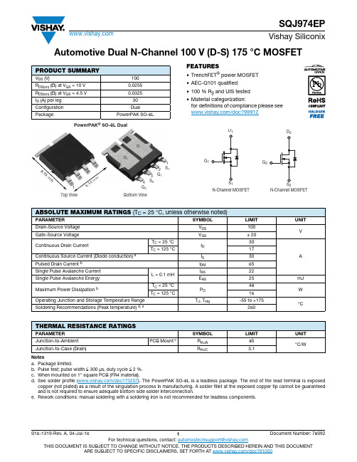
Automotive Dual N-Channel 100 V (D-S) 175 °C MOSFETFEATURES•TrenchFET ® power MOSFET •AEC-Q101 qualified •100 % R g and UIS tested•Material categorization:for definitions of compliance please see /doc?99912Notesa.Package limited.b.Pulse test; pulse width ≤ 300 μs, duty cycle ≤ 2 %.c.When mounted on 1" square PCB (FR4 material).d.See solder profile (/doc?73257). The PowerPAK SO-8L is a leadless package. The end of the lead terminal is exposed copper (not plated) as a result of the singulation process in manufacturing. A solder fillet at the exposed copper tip cannot be guaranteed and is not required to ensure adequate bottom side solder interconnection.e.Rework conditions: manual soldering with a soldering iron is not recommended for leadless components.PRODUCT SUMMARYV DS (V)100R DS(on) (Ω) at V GS = 10 V 0.0255R DS(on) (Ω) at V GS = 4.5 V 0.0325I D (A) per leg 30Configuration Dual PackagePowerPAK SO-8LPowerPAK ®S O-8L DualTop View6 .13 m1.15m m5m Bottom View2G 13S 24G 21S 1D 2D 1ABSOLUTE MAXIMUM RATINGS (T C = 25 °C, unless otherwise noted)PA AMETE SYMBOL LIMIT UNIT Drain-Source Voltage V DS100VGate-Source Voltage V GS ± 20Continuous Drain CurrentT C = 25 °C I D 30A T C = 125 °C17Continuous Source Current (Diode conduction) a I S 30Pulsed Drain Current bI DM 65Single Pulse Avalanche Current L = 0.1 mH I AS 22Single Pulse Avalanche Energy E AS 25mJ Maximum Power Dissipation bT C = 25 °C P D 48W T C = 125 °C 16Operating Junction and Storage Temperature Range T J , T stg-55 to +175°C Soldering Recommendations (Peak temperature) d, e260THERMAL RESISTANCE RATINGSPA AMETE SYMBOL LIMIT UNIT Junction-to-Ambient PCB Mount cR thJA 85°C/WJunction-to-Case (Drain)R thJC3.1Notesa.Pulse test; pulse width ≤ 300 μs, duty cycle ≤ 2 %.b.Guaranteed by design, not subject to production testing.c.Independent of operating temperature.Stresses beyond those listed under “Absolute Maximum Ratings” may cause permanent damage to the device. These are stress ratings only, and functional operation of the device at these or any other conditions beyond those indicated in the operational sections of the specifications is not implied. Exposure to absolute maximum rating conditions for extended periods may affect device reliability.SPECIFICATIONS (T C = 25 °C, unless otherwise noted)PA AMETE R SYMBOLTEST CONDITIONS MIN.TYP.MAX.UNITStaticDrain-Source Breakdown Voltage V DS V GS = 0 V, I D = 250 μA 100--V Gate-Source Threshold Voltage V GS(th)V DS = V GS , I D = 250 μA 1.5 2.0 2.5Gate-Source LeakageI GSS V DS = 0 V, V GS = ± 20 V--± 100nAZero Gate Voltage Drain Current I DSS V GS = 0 VV DS = 100 V --1μA V GS = 0 V V DS = 100 V, T J = 125 °C --50V GS = 0 V V DS = 100 V, T J = 175 °C--150On-State Drain Current aI D(on)V GS = 10 V V DS ≥ 5 V 15--A Drain-Source On-State Resistance aR DS(on)V GS = 10 V I D = 10 A -0.02100.0255ΩV GS = 10 V I D = 10 A, T J = 125 °C --0.0426V GS = 10 V I D = 10 A, T J = 175 °C--0.0539V GS = 4.5 VI D = 8 A-0.02700.0325Forward Transconductance b g fs V DS = 15 V, I D = 10 A-27-S Dynamic bInput Capacitance C issV GS = 0 V V DS = 25 V, f = 1 MHz -7851050pF Output CapacitanceC oss -405550Reverse Transfer Capacitance C rss -3050Total Gate Charge c Q gV GS = 10 V V DS = 50 V, I D = 5 A -1530nC Gate-Source Charge c Q gs -3-Gate-Drain Charge c Q gd -3-Gate Resistance R g f = 1 MHz0.65 1.41 2.20ΩTurn-On Delay Time c t d(on)V DD = 50 V, R L = 10 ΩI D ≅ 5 A, V GEN = 10 V, R g = 10 Ω-1020ns Rise Time ct r-510Turn-Off Delay Time c t d(off) -2040Fall Time c t f -510Source-Drain Diode Ratings and Characteristics bPulsed Current a I SM --65A Forward VoltageV SD I F = 10 A, V GS = 0 V-0.871.2VTransconductance Capacitance On-Resistance vs. Drain CurrentGate ChargeOn-Resistance vs. Gate-to-Source Voltage Drain Source Breakdown vs. Junction TemperatureThreshold Voltage Safe Operating AreaTHERMAL RATINGS(T A = 25 °C, unless otherwise noted)Normalized Thermal Transient Impedance, Junction-to-AmbientNormalized Thermal Transient Impedance, Junction-to-CaseNote•The characteristics shown in the two graphs- Normalized Transient Thermal Impedance Junction-to-Ambient (25 °C)- Normalized Transient Thermal Impedance Junction-to-Case (25 °C)are given for general guidelines only to enable the user to get a “ball park” indication of part capabilities. The data are extracted from single pulse transient thermal impedance characteristics which are developed from empirical measurements. The latter is valid for the part mounted on printed circuit board - FR4, size 1" x 1" x 0.062", double sided with 2 oz. copper, 100 % on both sides. The part capabilities can widely vary depending on actual application parameters and operating conditions.Vishay Silicon ix main tain s worldwide man ufacturin g capability. Products may be man ufactured at on e of several qualified location s. Reliability data for Silicon Technology and Package Reliability represent a composite of all qualified locations. For related documents such as package/tape drawings, part marking, and reliability data, see /ppg?78092.PowerPAK® SO-8L Case Outlinefor Al PartsNote•Millimeters will goverLIMETERSINCHESMIN.NOM.MAX.MIN.NOM.MAX.A 1.00 1.07 1.140.0390.0420.045A10.00-0.1270.00-0.005b 0.330.410.480.0130.0160.019b10.440.510.580.0170.0200.023b2 4.804.905.000.1890.1930.197b30.0940.004b40.470.019c 0.200.250.300.0080.0100.012D 5.00 5.13 5.250.1970.2020.207D1 4.80 4.90 5.000.1890.1930.197D2 3.86 3.96 4.060.1520.1560.160D3 1.631.73 1.830.0640.0680.072e 1.27 BSC0.050 BSCE 6.05 6.15 6.250.2380.2420.246E1 4.27 4.37 4.470.1680.1720.176E2 2.75 2.85 2.950.1080.1120.116F --0.15--0.006L 0.620.720.820.0240.0280.032L10.921.07 1.220.0360.0420.048K 0.510.020W 0.230.009W10.410.016W2 2.820.111W3 2.960.117q0°-10°0°-10°ECN: C15-1203-Rev. A, 07-Sep-15DWG: 6044PAD Pattern Vishay SiliconixRECOMMENDED MINIMUM PAD FOR PowerPAK® SO-8L DUALLegal Disclaimer Notice VishayDisclaimerALL PRODUCT, PRODUCT SPECIFICAT IONS AND DAT A ARE SUBJECT T O CHANGE WIT HOUT NOT ICE T O IMPROVE RELIABILITY, FUNCTION OR DESIGN OR OTHERWISE.Vishay Intertechnology, Inc., its affiliates, agents, and employees, and all persons acting on its or their behalf (collectively, “Vishay”), disclaim any and all liability for any errors, inaccuracies or incompleteness contained in any datasheet or in any other disclosure relating to any product.Vishay makes no warranty, representation or guarantee regarding the suitability of the products for any particular purpose or the continuing production of any product. To the maximum extent permitted by applicable law, Vishay disclaims (i) any and all liability arising out of the application or use of any product, (ii) any and all liability, including without limitation special, consequential or incidental damages, and (iii) any and all implied warranties, including warranties of fitness for particular purpose, non-infringement and merchantability.Statements regarding the suitability of products for certain types of applications are based on Vishay’s knowledge of typical requirements that are often placed on Vishay products in generic applications. Such statements are not binding statements about the suitability of products for a particular application. It is the customer’s responsibility to validate that a particular product with the properties described in the product specification is suitable for use in a particular application. Parameters provided in datasheets and / or specifications may vary in different applications and performance may vary over time. All operating parameters, including typical parameters, must be validated for each customer application by the customer’s technical experts. Product specifications do not expand or otherwise modify Vishay’s terms and conditions of purchase, including but not limited to the warranty expressed therein.Except as expressly indicated in writing, Vishay products are not designed for use in medical, life-saving, or life-sustaining applications or for any other application in which the failure of the Vishay product could result in personal injury or death. Customers using or selling Vishay products not expressly indicated for use in such applications do so at their own risk. Please contact authorized Vishay personnel to obtain written terms and conditions regarding products designed for such applications.No license, express or implied, by estoppel or otherwise, to any intellectual property rights is granted by this document or by any conduct of Vishay. Product names and markings noted herein may be trademarks of their respective owners.© 2017 VISHAY INTERTECHNOLOGY, INC. ALL RIGHTS RESERVED。
AOT8N80规格书

TO-220F
900V@150℃ 7.4A < 1.63Ω
D
AOT8N80
S D G
AOTF8N80
S GD
Absolute Maximum Ratings TA=25°C unless otherwise noted
Parameter
Symbol
Drain-Source Voltage
VDS
Gate-Source Voltage
Qrr
Body Diode Reverse Recovery Charge IF=8A,dI/dt=100A/µs,VDS=100V
1
10
µA
±100 nΑ
3.3 3.9 4.5
V
1.35 1.63 Ω
9
S
0.72 1
V
7.4
A
26
A
1100 1375 1650 pF
70 101 132 pF
6
11
16 pF
1.7 3.5 5.3
Ω
20
26
32
nC
7.3
nC
9.1
nC
ns
380 484 585 ns
4.5
6
7.5 µC
A. The value of R θJA is measured with the device in a still air environment with T A =25°C. B. The power dissipation PD is based on TJ(MAX)=150°C, using junction-to-case thermal resistance, and is more useful in setting the upper dissipation limit for cases where additional heatsinking is used.
MOSFET场效应管的应用及主要型号
MOSFET场效应管的应用及主要型号:型号封装主要参数应用领域PTP50N06 TO-220 50A/60V,RDS(on)=22mΩ 电动车充电器,控制器,工业控制、机箱电源、逆变器、(VGS=10V,ID=25A)PTP830 TO-220 5A/500V,RDS(on)=1.5Ω UPS电源、电源控制器.电动车控制器,转换器.充电器、小家电、智能麻将机控制(VGS=10V,ID=2.5A)PTP840 TO-220 9A/500V,RDS(on)=0.8Ω(VGS=10V,ID=4A)PTD2N60 TO-252 1.9A/600V,RDS(on)=4.7Ω 节能灯、充电器、开关电源、LCD显示器、电子镇流器(VGS=10V,ID=0.95A)PTU2N60 TO-251 1.9A/600V,RDS(on)=4.7Ω(VGS=10V,ID=0.95A)PTF2N60 TO-220F 2A/600V,RDS(on)=4.7Ω(VGS=10V,ID=1.0A)PTP2N60 TO-220 2A/600V,RDS(on)=4.7Ω(VGS=10V,ID=1.0A)PTF5N60 TO-220F 4.5A/600V,RDS(on)=2.5Ω 风扇控制板,控制电源,LED驱动电源,路灯电源,灯杯电源,LCD电源、机箱电源、逆变器、(VGS=10V,ID=2.25A)PTP5N60 TO-220 4.5A/600V,RDS(on)=2.5Ω(VGS=10V,ID=2.25A)PTF8N60 TO-220F 7.5A/600V,RDS(on)=1.2Ω 电动车控制器,电源工具,汽车调压器、机箱电源、逆变器、(VGS=10V,ID=3.75A)PTP8N60 TO-220 7.5A/600V,R DS(on)=1.2Ω(VGS=10V,ID=3.75A)PTD5N50 TO-252 4A/500V,RDS(on)=0.8Ω HID电子镇流器,节能灯,开关电源、(VGS=10V,ID=4.0A)PTP630 TO-220 9A/200V,RDS(on)=0.4Ω 风扇控制板,控制电源,LED驱动电源,路灯电源,灯杯电源,LCD电源、机箱电源、逆变器、(VGS=5V,ID=5.4A)PTP640 TO-220 18A/200V,RDS(on)=0.18Ω(VGS=5V,ID=9.0A)PTP9N20 TO-220 电动车控制器,电源工具,汽车调压器、机箱电源、逆变器、PTF9N20 TO-220FPTP10N40 TO-220 18A/200V,RDS(on)=0.18Ω HID电子镇流器,节能灯,开关电源、(VGS=5V,ID=9.0A)PTF10N40 TO-220F 工控设备,电动车控制器,电源工具,汽车调压器、机箱电源、逆变器、PTP10N60 TO-220 9.5/600V,RDS(on)=0.73Ω(VGS=5V,ID=4.75A)PTF10N60 TO-220F 9.5/600V,RDS(on)=0.73Ω 工业电源,HID电子镇流器,节能灯,开关电源、(VGS=5V,ID=4.75A)PTP12N60 TO-220 12A/600V,RDS(on)=0.65Ω 风扇控制板,控制电源,LED驱动电源,路灯电源,灯杯电源,LCD电源、机箱电源、逆变器、(VGS=10V,ID=6.0A)PTF12N60 TO-220F 12A/600V,RDS(on)=0.65Ω(VGS=10V,ID=6.0A)PTP18N20 TO-220 18A/600V,RDS(on)=0.145Ω 电动车控制器,电源工具,汽车调压器、机箱电源、逆变器、(VGS=10V,ID=9.0A)PTF18N20 TO-220F 18A/600V,RDS(on)=0.145Ω(VGS=10V,ID=9.0A)SI2300 SOT-23 2.3A/20V,RDS(on)=70mΩ 可作电源管理、电池保护,负载开关等(VGS=10V,ID=3.0A)用途。
NMLU1210全桥矩流双极性N型晶体管说明书
NMLU1210TWG NMLU1210TWG.NMLU1210Full Bridge RectifierDual 20 V N −Channel with dual 3.2 A Schottky Barrier Diode, 4.0 x 4.0 x 0.5 mm m Cool ™ PackageFeatures•Full −Bridge Rectifier Block •Up to 3.2 A operation•Low R DS(on ) MOSFET to minimize conduction loss •Low gate charge MOSFET •Low VF Schottky diode•Ultra Low Inductance Package•This Device uses Halogen −Free Molding Compound •These are Pb −Free DevicesApplications•Wireless Charging •AC −DC Rectification•Optimized for Power Management Applications for PortableProducts, such as Cell Phones, PMP, DSC, GPS, and othersRECTIFIER MAXIMUM RATINGS (T J = 25°C unless otherwise stated)ParameterSymbol ValueUnit Input voltage between two MOSFET drain V LL 20V Bridge Operating Junction and StorageTemperatureT J , T STG−55 to 125°C Lead Temperature for Soldering Purposes (1/8” from case for 10 s)T L 260°C Continuous Drain Current R _JA (Note 1)T A = 25°C I O2.2AT A = 85°C 1.16Power Dissipation R _JA (Note 1)T A = 25°C P D 1.2W T A = 85°C 0.47Continuous Drain Current R _JA t < 5 s (Note 1)T A = 25°C I O 3.2A T A = 85°C 1.88Power Dissipation R _JA t < 5 s (Note 1)T A = 25°C P D 2.34W T A = 85°C 0.94Continuous Drain Current R _JA (Note 2)T A = 25°C I O 1.16A T A = 85°C 0.6Power Dissipation R _JA (Note 2)T A = 25°C P D 0.47W T A = 85°C0.185Stresses exceeding Maximum Ratings may damage the device. Maximum Ratings are stress ratings only. Functional operation above the Recommended Operating Conditions is not implied. Extended exposure to stresses above the Recommended Operating Conditions may affect device reliability.1.Surface −mounted on FR4 board using 1 in sq pad size (Cu area = 1.127 in sq [2 oz] including traces).2.Surface −mounted on FR4 board using the minimum recommended pad size of 30 mm 2, 2 oz. Cu.Device Package Shipping †ORDERING INFORMATIONUDFN CASE 517BS20 V20 V17 m W @ 10 V23 m W @ 4.5 V 0.45 VR DS(on) TYP 3.2 A3.2 AI D MAX V (BR)DSS MOSFETSCHOTTKY DIODEV R MAX I F MAX V F TYP RECTIFIERMARKING DIAGRAMPIN CONNECTIONSNMLU1210TWGUDFN (Pb −Free)3000 / Tape & Reel†For information on tape and reel specifications,including part orientation and tape sizes, please refer to our T ape and Reel Packaging Specifications Brochure, BRD8011/D.Vout L1_2GND2GND2(Top View)4.0 4.0 mm m Cool Pin Connections(Top View)1210AYWW GG1210= Specific Device Code A = Assembly Location Y = Year WW = Work Week G = Pb −Free Package(*Note: Microdot may be in either location)THERMAL RESISTANCE RATINGSParameter Symbol Max Unit Junction−to−Ambient – Steady State (Note 3)RθJA82.5°C/W Junction−to−Ambient – t ≤ 5 s (Note 3)RθJA42.5Junction−to−Ambient – Steady State min Pad (Note 4)RθJA2093.Surface−mounted on FR4 board using 1 in sq pad size (Cu area = 1.127 in sq [2 oz] including traces).4.Surface−mounted on FR4 board using the minimum recommended pad size of 30 mm2, 2 oz. Cu.BRIDGE ELECTRICAL CHARACTERISTICS (T J = 25°C unless otherwise specified)Parameter Symbol Test Condition Min Typ Max Unit ON CHARACTERISTICSRectifying Forward Voltage (Note 5)V fd2Input voltage V LL = ±5 V;The output current of Rectifier I out = 2 A0.45.56VRectifier leakage current I leak Input voltage V LL = 16 V;No Load on the Rectifier output311000uARectifier Reverse leakage current I rleak Input voltage V LL = 0 V;The output voltage of the RectifierV out = 5 V211000uA 5.Pulse Test: pulse width ≤ 300 m s, duty cycle ≤ 2%MOSFET ELECTRICAL CHARACTERISTICS (T J = 25°C unless otherwise specified)Parameter Symbol Test Condition Min Typ Max Unit ON CHARACTERISTICSGate Threshold Voltage V GS(TH)V GS = VDS, I D = 250 m A 1.2 2.2VNegative Threshold Temperature Coefficient V GS(TH) /T J4mV/°CDrain−to−Source On Resistance(Note 6)R DS(on)V GS = 10 V, I D = 3.2 A1726m W V GS = 4.5 V, I D = 3.2 A2332Forward Transconductance g FS VDS = 10 V, I D = 2.0 A 3.5S DRAIN−SOURCE DIODE CHARACTERISTICSForward Diode Voltage (Note 6)V SD V GS = 0 V, I S = 2.0 A T J = 25°C0.79VT J = 125°C0.656.Pulse Test: pulse width ≤ 300 m s, duty cycle ≤ 2%SCHOTTKY DIODE ELECTRICAL CHARACTERISTICS (T J = 25°C unless otherwise specified)Parameter Symbol Test Condition Min Typ Max UnitMaximum Instantaneous Forward Voltage (Note 7)V F I F = 1.0 A0.36VI F = 2.0 A0.41Maximum Instantaneous ReverseCurrentI R V R = 20 V0.04mA7.Pulse Test: pulse width ≤ 300 m s, duty cycle ≤ 2%SCHOTTKY DIODE ELECTRICAL CHARACTERISTICS (T J = 100°C unless otherwise specified)Parameter Symbol Test Condition Min Typ Max UnitMaximum Instantaneous ForwardVoltage (Note 8)V F I F = 1.0 A0.29V I F = 2.0 A0.36Maximum Instantaneous ReverseCurrentI R V R = 20 V4mA8.Pulse Test: pulse width ≤ 300 m s, duty cycle ≤ 2%9.For detailed MOSFET and Diode parameters, please refer to the ON Semiconductor datasheets of NTTFS4930N and MBR230LSFT1G.The test on each individual die is limited to the system package.Figure 1. Typical Application CircuitGND1 and GND2 are not internally connected. The user should make the connection in the PCB design.TYPICAL PERFORMANCE CURVES(T J = 25°C unless otherwise specified)0.20.40.60.81.01.21.41.61.8Figure 2. Bridge Typical Forward Voltage Dropat V in . 5 VV F , INSTANTANEOUS FORWARD VOLTAGE (V)I F , I N S T A N T A N E O U S F O R W A R D C U R R E N T (A )00.20.40.60.8 1.0 1.2 1.4 1.6 1.8Figure 3. Bridge Maximum Forward VoltageDrop at V in . 5 VV F , INSTANTANEOUS FORWARD VOLTAGE (V)I F , I N S T A N T A N E O U S F O R W A R D C U R R E N T (A )Figure 4. Output Leakage at 5 V Bias vs.Junction TemperatureT J , TEMPERATURE JUNCTION (°C)O U T P U T L E A K A G E (m A )Figure 5. Input Leakage at 16 V vs. JunctionTemperatureT J , TEMPERATURE JUNCTION (°C)I L E A K , O U T P U T L E A K A G E (m A )Figure 6. FET Typical On −Resistance vs.Gate −to −Source Voltage ( from 3 V to 10 V)7006005004003002001000V GS (V)R D S (on ) (m W )2.03.04.05.06.07.08.09.010Figure 7. FET Typical On −Resistance vs.Gate −to −Source VoltageV GS , GATE −TO −SOURCE VOLTAGE (V)R D S (o n ) (m W )TYPICAL PERFORMANCE CURVES(T J = 25°C unless otherwise specified)1010.1Figure 8. Schottky Typical Forward Current vs.Forward Voltage V F , INSTANTANEOUS FORWARD VOLTAGE (V)I F , I N S T A N T A N E O U S F O R W A R D C U R R E N T (A )Figure 9. Schottky Typical Reverse Current vs.Reverse VoltageV R , INSTANTANEOUS REVERSE VOLTAGE (V)I R , I N S T A N T A N E O U S R E V E R S E C U R R E N T (m A )PACKAGE DIMENSIONSUDFN8 4x4, 0.8P CASE 517BS ISSUE ANOTES:1.DIMENSIONING AND TOLERANCING PER ASME Y14.5M, 1994.2.CONTROLLING DIMENSION: MILLIMETERS.3.DIMENSION b APPLIES TO PLATEDTERMINAL AND IS MEASURED BETWEEN 0.15 AND 0.25MM FROM TERMINAL TIP .4.COPLANARITY APPLIES TO THE EXPOSED PAD AS WELL AS THE TERMINALS.5.POSITIONAL TOLERANCE APPLIES TO ALL OF THE EXPOSED PADS.DIM MIN MAX MILLIMETERS A 0.450.55A10.000.05A30.13 REF b 0.200.30D 4.00 BSC D2 2.10 2.30E 4.00 BSC E2 2.50 2.70F 3.55 BSC L 0.300.50L10.000.15BOTTOM VIEWSEATINGPLANE*For additional information on our Pb −Free strategy and soldering details, please download the ON Semiconductor Soldering and Mounting Techniques Reference Manual, SOLDERRM/D.SOLDERING FOOTPRINT*DETAIL AALTERNATE CONSTRUCTIONSDETAIL BALTERNATE CONSTRUCTIONSL30.130.23DIMENSIONS: MILLIMETERSD30.90 1.10E3 1.00 1.20e 0.80 BSC RECOMMENDED2XDETAIL CON Semiconductor and are registered trademarks of Semiconductor Components Industries, LLC (SCILLC). SCILLC owns the rights to a number of patents, trademarks,copyrights, trade secrets, and other intellectual property. A listing of SCILLC’s product/patent coverage may be accessed at /site/pdf/Patent −Marking.pdf. SCILLC reserves the right to make changes without further notice to any products herein. SCILLC makes no warranty, representation or guarantee regarding the suitability of its products for any particular purpose, nor does SCILLC assume any liability arising out of the application or use of any product or circuit, and specifically disclaims any and all liability, including without limitation special, consequential or incidental damages. “Typical” parameters which may be provided in SCILLC data sheets and/or specifications can and do vary in different applications and actual performance may vary over time. All operating parameters, including “Typicals” must be validated for each customer application by customer’s technical experts. SCILLC does not convey any license under its patent rights nor the rights of others. SCILLC products are not designed, intended, or authorized for use as components in systems intended for surgical implant into the body, or other applications intended to support or sustain life, or for any other application in which the failure of the SCILLC product could create a situation where personal injury or death may occur. Should Buyer purchase or use SCILLC products for any such unintended or unauthorized application, Buyer shall indemnify and hold SCILLC and its officers, employees, subsidiaries, affiliates, and distributors harmless against all claims, costs, damages, and expenses, and reasonable attorney fees arising out of, directly or indirectly,any claim of personal injury or death associated with such unintended or unauthorized use, even if such claim alleges that SCILLC was negligent regarding the design or manufacture of the part. SCILLC is an Equal Opportunity/Affirmative Action Employer. This literature is subject to all applicable copyright laws and is not for resale in any manner.PUBLICATION ORDERING INFORMATIONm Cool is a trademark of Semiconductor Components Industries, LLC (SCILLC).NMLU1210TWG NMLU1210TWG.。
AO3404 N-Channel MOSFET 晶体管数据手册说明书
FEATURESThe AO3404uses advanced trench technology to provide excellent R DS(ON)and low gate charge.This device maybe used as a load switch or in PWM applications.Absolute Maximum Ratings (TA=25oC, unless otherwise noted)AO3404 N-ChannelMOSFETSOT-231.Gate2.Source3.DrainParameter Symbol Value Unit Drain-source voltage V DS 30 V Gate-source voltage V GS±20 V Continuous drain current (t ≤10s) I D 5.8 A Pulsed drain current *I DM30 A Thermal resistance from junction to ambient RθJA 357 ℃/WJunction temperature T J 150 ℃Storage temperature T stg -55~150 ℃Repetitive rating : Pulse width limited by maximum junction temperature.Electrical Characteristics (TA=25°C, unless otherwise noted)AO3404ParameterSymbol Test Condition Min Typ Max UnitsSTATIC PARAMETERSDrain-source breakdown voltage V (BR) DSSV GS = 0V, I D =250µA 30V Zero gate voltage drain current I DSS V DS =30V,V GS = 0V 1µAGate-body leakage current I GSS V GS =±20V, V DS = 0V±100 nA Gate threshold voltageV GS(th) V DS =V GS , I D =250µA 13VV GS =10V, I D =5.8A 30 m Ω Drain-source on-resistance (note 1) R DS(on) V GS =4.5V, I D =4.8A42 m Ω Forward tranconductance (note 1) g FS V DS =5V, I D =5.8A 5 S Diode forward voltageV SDI S =1A1 VDYNAMIC PARAMETERS (note 2)Input capacitance C iss 820 pF Output capacitanceC oss 118 pF Reverse transfer capacitance C rss V DS =15V,V GS =0V,f =1MHz85 pFGate resistanceR gV DS =0V,V GS =0V,f =1MHz 1.5 ΩSWITCHING PARAMETERS (note 2)Turn-on delay time t d(on)6.5 ns Turn-on rise time t r3.1 ns Turn-off delay time t d(off) 15.1 ns Turn-off fall time t fV GS =10V,V DS =15V, R L =2.6Ω,R GEN =3Ω2.7 nsNote :1. Pulse Test : Pulse width ≤300µs, duty cycle ≤0.5%.2. These parameters have no way to verify.AO3404Typical CharacteristicsV GS (Volts)Figure 2: Transfer Characteristics (Note E)V DS (Volts)Fig 1: On-Region Characteristics (Note E)I D (A )AO3404Typical Characteristics123456Q g (nC)Figure 7: Gate-Charge Characteristics V G S (V o l t s )51015202530V DS (Volts)Figure 8: Capacitance Characteristics C a p a c i t a n c e (p F )。
ao4410场效应管参数
ao4410场效应管参数
AO4410是一种N沟道场效应管(MOSFET),常用于功率放大和开关电路。
它具有以下主要参数:
1. 额定电压(VDS),AO4410的额定漏极-源极电压范围通常在20V到30V之间,这意味着在正常工作条件下,它可以承受的最大电压范围。
2. 额定电流(ID),AO4410的最大漏极电流通常在3安培到5安培之间,这表示在正常工作条件下,它可以通过的最大电流。
3. 阈值电压(VGSth),这是场效应管的栅极-源极阈值电压,一般在1V到2V之间。
当栅极电压超过这个值时,场效应管开始导通。
4. 导通电阻(RDS(on)),这是场效应管的漏极-源极导通时的电阻值,通常在几毫欧姆到几十毫欧姆之间。
这个值越小,表示场效应管导通时的损耗越小。
5. 开关特性,AO4410具有较快的开关特性,能够在较短的时
间内完成通断转换,适用于一些要求高频率开关的场合。
总的来说,AO4410是一款性能稳定、可靠性高的场效应管,适用于各种电子设备中的功率放大和开关控制电路。
在使用时,需要根据具体的电路设计要求和工作环境来选择合适的参数范围,以确保电路的稳定性和可靠性。
- 1、下载文档前请自行甄别文档内容的完整性,平台不提供额外的编辑、内容补充、找答案等附加服务。
- 2、"仅部分预览"的文档,不可在线预览部分如存在完整性等问题,可反馈申请退款(可完整预览的文档不适用该条件!)。
- 3、如文档侵犯您的权益,请联系客服反馈,我们会尽快为您处理(人工客服工作时间:9:00-18:30)。
Symbol
Typ Max 648389120R θJL 5370Maximum Junction-to-Lead C
Steady-State
°C/W
Thermal Characteristics Parameter
Units Maximum Junction-to-Ambient A t ≤ 10s R θJA °C/W Maximum Junction-to-Ambient A Steady-State °C/W AO8810
Symbol
Min Typ
Max
Units BV DSS 20
V 1T J =55°C
5±1µA ±10
µA V GS(th)0.40.61V I D(ON)30
A 16.520T J =125°C
23282024m Ω2432m Ωg FS 29S V SD 0.76
1V I S
2.5
A C iss 1160
pF C oss 187pF C rss 146pF R g 1.5ΩQ g 16nC Q gs 0.8nC Q gd 3.8nC t D(on) 6.2ns t r 12.7ns t D(off)51.7ns t f 16ns t rr 17.7ns Q rr 6.7
nC
Body Diode Reverse Recovery Time Body Diode Reverse Recovery Charge
I F =7A, dI/dt=100A/µs
Drain-Source Breakdown Voltage On state drain current
I D =250µA, V GS =0V V GS =4.5V, V DS =5V V GS =4.5V, I D =7A
Reverse Transfer Capacitance I F =7A, dI/dt=100A/µs Electrical Characteristics (T J =25°C unless otherwise noted)STATIC PARAMETERS Parameter
Conditions I DSS µA Gate Threshold Voltage V DS =V GS I D =250µA V DS =16V, V GS =0V
Zero Gate Voltage Drain Current I GSS Gate-Body leakage current V DS =0V, V GS =±4.5V R DS(ON)
Static Drain-Source On-Resistance
Forward Transconductance Diode Forward Voltage m ΩV GS =2.5V, I D =5.5A I S =1A,V GS =0V V DS =5V, I D =7A V GS =1.8V, I D =5A
Turn-On Rise Time Turn-Off DelayTime V GS =5V, V DS =10V, R L =1.35Ω, R GEN =3Ω
Gate resistance V GS =0V, V DS =0V, f=1MHz
Turn-Off Fall Time SWITCHING PARAMETERS Total Gate Charge V GS =4.5V, V DS =10V, I D =7A
Gate Source Charge Turn-On DelayTime DYNAMIC PARAMETERS V GS =0V, V DS =10V, f=1MHz Gate Drain Charge V DS =0V, V GS =±8V Maximum Body-Diode Continuous Current
Input Capacitance Output Capacitance A: The value of R θJA is measured with the device mounted on 1in 2
FR-4 board with 2oz. Copper, in a still air environment with T A =25°C. The value in any a given application depends on the user's specific board design. The current rating is based on the t ≤ 10s thermal resistance rating.
B: Repetitive rating, pulse width limited by junction temperature.
C. The R θJA is the sum of the thermal impedence from junction to lead R θJL and lead to ambient.
D. The static characteristics in Figures 1 to 6,12,14 are obtained using 80 µs pulses, duty cycle 0.5% max.
E. These tests are performed with the device mounted on 1 in 2
FR-4 board with 2oz. Copper, in a still air environment with T A =25°C. The SOA curve provides a single pulse rating.。