DDS-232光电隔离器用户说明书
隔离232方案选择

(1)传统方法,使用光耦TLP521
注意:VCC为5V电源,是由变压器的另一组绕线整流、滤波、稳压产生+5V。
使用光耦6N137
(2)使用ADuM公司的信号隔离芯片ADUM1201
采用ADUM1201实现3.3V控制系统与5V供电的RS-232收发器的隔离通信
注意:需要一个+5V隔离电源,可以由DCDC产生,也可由变压器的另一组绕线整流、滤波、稳压产生+5V。
(3)使用ADuM公司的带DCDC信号隔离芯片ADUM5241
其内部集成一个5V-5V的内部DC/DC隔离电源,当VDD1输入一个5V的外接电源时,VISO会输出一个+5V/10mA的电压。
可以为后端的RS-232收发器供电;但当前端输入3.3V电压的时候,内部DC/DC隔离电源则不工作,后端的VISO需另外接电源供电。
(3)使用ADuM公司的带232隔离芯片ADuM3251
图中采用三极管加上拉电阻升压的方法将 3.3V的输入信号拉升到5V,输入到ADuM3251E的Tin引脚,而ADuM3251E的Rout引脚5V输出信号经电阻分压,转换成3.3V 信号输入到以3.3V电源工作的控制器中。
需要注意的是,上拉电阻及限流电阻都会不通程度的影响数据传输速率。
ADuM3251E外围共需6个电容,2个瓷片104电容,和4个电荷泵电容,泵电容是很重要的,用来稳定RS-232的输出信号,保证足够的升压,因此推荐使用耐压16V,0.1uF 的电解电容。
232 TACT 电子开关说明书

TɹNBY
4PMEFSJOHUFNQFSBUVSF
ˆNBY
%VSBUJPOPGJNNFSTJPO
TNBY
/VNCFSPGTPMEFSJOH
UJNFTNBY
/PUFT 1SFWFOUqVYQFOFUSBUJPOGSPNUIFUPQTJEFPGUIF5"$54XJUDI5. 4XJUDIUFSNJOBMTBOEB1$CPBSETIPVMEOPUCFDPBUFEXJUIqVYQSJPSUPTPMEFSJOH 5IFTFDPOETPMEFSJOHTIPVMECFEPOFBGUFSUIFTXJUDIJTTUBCMFXJUIOPSNBMUFNQFSBUVSF 6TFUIFqVYXJUIBTQFDJpDHSBWJUZPGNJO ʢ & $ 4 CZ5 " .6 3 " $ 03 1 03 " 5 *0/ PS FRVJWB MFOUT ʣ
Low contact resistance
—
—
—
—
—
—
High operation force Low contact resistance
—
—
Dustproof
—
—
—
—
—
—
—
—
IP standard
—
—
—
—
—
—
—
—
Top push
—
—
●
●
Operating
direction
Side push
●
●
Notes 1. The automotive operating temperature range to be individually discussed upon request. 2. ● Indicates applicability to all products in the series, while ○ indicates applicability to some products in the series.
DC USB 232 ISO通信转换器说明书
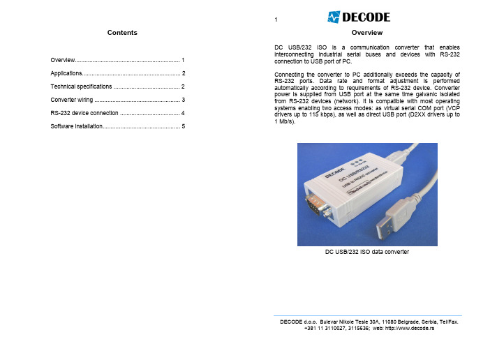
Communication connectors Compliance Data rate and format Maximum distance Supported operating systems Cable in set LED indicators Galvanic isolation Power supply
DECODE d.o.o. Bulevar Nikole Tesle 30A, 11080 Belgrade, Serbia, Tel/Fax. +381 11 3110027, 3115636; web: http://www.decode.rs
Input
Clear To Send
Input
Ring indicator
5
Software installation
Plug DC USB/232 ISO converter to USB port of PC first, by using included USB cable. It can be hot-plugged without powering the PC off. After a few moments, following system message will show (images are taken from Win XP operating system – other OS can have a bit different appearance):
DECODE d.o.o. Bulevar Nikole Tesle 30A, 11080 Belgrade, Serbia, Tel/Fax. +381 11 3110027, 3115636; web: http://www.decode.rs
双通道数字隔离器 EVM 用户指南说明书
User's GuideSLLU098C–June2007–Revised December2010Dual-Channel Digital Isolator EVMContents1Introduction (1)1.1Overview (2)1.2Functional Configuration of the Dual-Channel Digital Isolator (2)1.3The EVM Signal Paths of the ISO7220x,ISO7221x,and ISO742x Isolators (3)1.4The ISO7220x and ISO7420x EVM Configuration (5)1.5The ISO7221x and ISO7421x EVM Configuration (6)2EVM Setup and Operation (7)2.1Overview (7)List of Figures1The ISO7x20x and ISO7x21x Pinouts (2)2The ISO7x20x Same-Channel Direction Schematic (3)3The ISO7x21x Opposing-Channel Direction Schematic (4)4ISO7220x and ISO7420x EVM,Top View (5)5ISO7220x and ISO7420x EVM,Bottom View (5)6The ISO7221x and ISO7421x EVM Top View (6)7The ISO7221x and ISO7421x EVM Bottom View (6)8Basic EVM Operation (7)9Typical Input and Output Waveforms (7)List of Tables1ISO7220x and ISO7420x EVM Connections (3)2ISO7221x and ISO7421x EVM Connections (4)1IntroductionThis user's guide details the evaluation module(EVM)operation of the factory installed ISO7421dual-channel digital isolator;however,the EVM board may be reconfigured by a user for use withISO7220A,ISO7220B,ISO7220C,ISO7220M,ISO7420,ISO7420M or ISO7420F same-channel direction isolators and the ISO7221A,ISO7221B,ISO7221C,ISO7221M,ISO7421,ISO7421M or ISO7421Fopposing-channel direction isolators.This guide also explains the user configurable I/O loads for both dual-channel isolator EVM configurations, and presents a typical lab setup with input and output waveforms.1 SLLU098C–June2007–Revised December2010Dual-Channel Digital Isolator EVM Submit Documentation FeedbackISO7x21xGND2Vcc2Vcc1GND1OUTB INA OUTA INB ISO7x20xGND2Vcc2Vcc1GND1OUTB INAOUTA INBIntroduction 1.1OverviewThe ISO7220x,ISO7221x,and ISO742X dual digital isolators have a logic input and output bufferseparated by a silicon oxide (SiO 2)insulation ed in conjunction with isolated power supplies,these devices block high voltage,isolate grounds,and prevent noise currents on a data bus or othercircuits from entering the local ground and interfering with or damaging sensitive circuitry.A binary input signal is conditioned,translated to a balanced signal,and then differentiated by thecapacitive isolation barrier.Across the isolation barrier,a differential comparator receives the logictransition information,then sets or resets a flip-flop and the output circuit accordingly.A periodic update pulse is sent across the barrier to ensure the proper dc level of the output.If this dc-refresh pulse is not received for more than 4m s,the input is assumed to be unpowered or not functional,and the failsafecircuit drives the output to a logic-high state.For ISO7420F and ISO7421F,the failsafe circuit drives the output to a logic-low state.CAUTIONNote that although these devices provide galvanic isolation of up to 4000V,thisEVM cannot be used for isolation voltage testing.It is designed for theexamination of device operating parameters only and will be damaged if highvoltage (>5.5V)is applied anywhere in the circuit.1.2Functional Configuration of the Dual-Channel Digital IsolatorThe pin-outs of the dual-channel digital isolators are displayed in Figure 1.The EVM comes with anISO7421installed;however,the user may reconfigure the EVM for use with any of the footprints.Figure 1.The ISO7x20x and ISO7x21x PinoutsThe ISO7220A,ISO7220B,ISO7220C,ISO7221A,ISO7221B and ISO7221C have TTL input thresholds and an input noise filter that prevents transient pulses of up to 2ns in duration from being passed to the output of the device.The ISO7220M and ISO7221M have a CMOS Vcc/2input threshold,but do not have the noise filter and the additional propagation delay.2Dual-Channel Digital Isolator EVM SLLU098C–June 2007–Revised December 2010Submit Documentation FeedbackV CC1(Banana Jack P1)V CC2(Banana Jack P2)GND1(Banana Jack P3)GND2(Banana Jack P4) Introduction1.3The EVM Signal Paths of the ISO7220x,ISO7221x,and ISO742x IsolatorsThis multifunctional EVM is designed with signal paths shown in Figure 1,Figure 2,and Figure 3for the evaluation of the ISO7220x and ISO7221x dual-channel isolators.Figure 2.The ISO7x20x Same-Channel Direction SchematicTable 1.ISO7220x and ISO7420x EVM ConnectionsConnectionLabel Description J1SMA connector to the INB input,pin 3J2SMA connector to the OUTB output,pin 6J3SMA connector to the INA input,pin 2J4SMA connector to the OUTA output,pin 7P1V CC1Input power supply banana jack P2V CC2Output power supply banana jack P3GND1Input power ground connection banana jack P4GND2Output power ground connection banana jack JMP13-pin jumper V CC1,input,GND1JMP23-pin jumper used to monitor OUTB with scope probe JMP33-pin jumper –V CC1,input,GND1JMP43-pin jumper used to monitor OUTA with scope probe3SLLU098C–June 2007–Revised December 2010Dual-Channel Digital Isolator EVM Submit Documentation FeedbackIntroduction V CC1(Banana Jack P1)V CC2(Banana Jack P2)GND1(Banana Jack P3)GND2(Banana Jack P4)Figure3.The ISO7x21x Opposing-Channel Direction SchematicTable2.ISO7221x and ISO7421x EVM ConnectionsConnection Label DescriptionJ1SMA connector to the INB input,pin3J2SMA connector to the OUTB output,pin6J3SMA connector to the OUTA output,pin2J4SMA connector to the INA input,pin7P1V CC1Input power supply banana jackP2V CC2Output power supply banana jackP3GND1Input power ground connection banana jackP4GND2Output power ground connection banana jackJMP13-pin jumper V CC1,input,GND1JMP23-pin jumper used to monitor OUTB with scope probeJMP33-pin jumper used to monitor OUTA with scope probeJMP43-pin jumper V CC2,input,GND24Dual-Channel Digital Isolator EVM SLLU098C–June2007–Revised December2010Submit Documentation Feedback Introduction1.4The ISO7220x and ISO7420x EVM ConfigurationThe ISO7220x EVM configuration has SMA connectors (J1and J3)set up as the input to the INA (pin 2)and INB (pin 3)of the ISO7220M in Figure 1and Figure 2.R2and R8are 0-Ωinput series resistorsshown in Figure 4,and are located next to the J1and J3input connectors.R1and R5are 50-Ωresistors from each input to ground,and are located on the bottom of the board as shown in Figure 5.Figure 4.ISO7220x and ISO7420x EVM,Top ViewThe output channel configuration of the ISO7220x EVM has the OUTA (pin 7)and OUTB (pin 6)ofFigure 1and Figure 2connected to SMA connector (J2and J4)through 0-Ωseries resistor,R4and R6.Figure 5.ISO7220x and ISO7420x EVM,Bottom ViewThe pads for R3,R7,C1,C12,C13and C14are available on the bottom of the EVM for varied loadingconditions if desired by a user.5SLLU098C–June 2007–Revised December 2010Dual-Channel Digital Isolator EVM Submit Documentation FeedbackIntroduction 1.5The ISO7221x and ISO7421x EVM ConfigurationThe ISO7221x EVM configuration has SMA connectors (J4and J1)set up as the input to the INA (pin 7)and INB (pin 3)of the ISO7221x in Figure 1and Figure 3.R2and R6are 0-Ωinput series resistors shown in Figure 6,and are located next to the J1and J4input connectors.Figure 6.The ISO7221x and ISO7421x EVM Top ViewThe output channel configuration of the ISO7221x EVM has the OUTA (pin 2)and OUTB (pin 6)ofFigure 1and Figure 3connected to SMA connector (J3and J2)through 0-Ωseries resistor,R8and R4.R1and R7are 50-Ωresistors from each input to ground on the bottom of the board shown in Figure 7.Figure 7.The ISO7221x and ISO7421x EVM Bottom ViewThe pads for R3,R5,C1,C12,C13and C14are available on the bottom of the EVM for varied loading conditions if desired by a user.6Dual-Channel Digital Isolator EVM SLLU098C–June 2007–Revised December 2010Submit Documentation Feedback EVM Setup and Operation 2EVM Setup and OperationThis section includes the setup and operation of the EVM for parameter performance evaluation.Typical waveforms are included.2.1OverviewThe basic setup in Figure 5has the two power supplies required to evaluate isolator performance with3.3-V on one side and 3.3-V on the other.If both sides are to be evaluated at the same supply voltage,only one power supply is required and can be used to power both sides of the EVM.CAUTIONNote that this EVM is for operating parameter performance evaluation only andnot designed for isolation voltage testing.Any voltage applied above the 5.5-Vmaximum recommended operating voltage of the digital isolators will damagethe EVM.Figure 8.Basic EVM OperationIn Figure 8,the J3input to the EVM is a 20MHz pulse displayed on channel 1in Figure 9.The J4output of the EVM is channel 2.Figure 9.Typical Input and Output Waveforms7SLLU098C–June 2007–Revised December 2010Dual-Channel Digital Isolator EVM Submit Documentation FeedbackEVALUATION BOARD/KIT IMPORTANT NOTICETexas Instruments(TI)provides the enclosed product(s)under the following conditions:This evaluation board/kit is intended for use for ENGINEERING DEVELOPMENT,DEMONSTRATION,OR EVALUATION PURPOSES ONLY and is not considered by TI to be a finished end-product fit for general consumer use.Persons handling the product(s)must have electronics training and observe good engineering practice standards.As such,the goods being provided are not intended to be complete in terms of required design-,marketing-,and/or manufacturing-related protective considerations,including product safety and environmental measures typically found in end products that incorporate such semiconductor components or circuit boards.This evaluation board/kit does not fall within the scope of the European Union directives regarding electromagnetic compatibility,restricted substances(RoHS),recycling (WEEE),FCC,CE or UL,and therefore may not meet the technical requirements of these directives or other related directives.Should this evaluation board/kit not meet the specifications indicated in the User’s Guide,the board/kit may be returned within30days from the date of delivery for a full refund.THE FOREGOING WARRANTY IS THE EXCLUSIVE WARRANTY MADE BY SELLER TO BUYER AND IS IN LIEU OF ALL OTHER WARRANTIES,EXPRESSED,IMPLIED,OR STATUTORY,INCLUDING ANY WARRANTY OF MERCHANTABILITY OR FITNESS FOR ANY PARTICULAR PURPOSE.The user assumes all responsibility and liability for proper and safe handling of the goods.Further,the user indemnifies TI from all claims arising from the handling or use of the goods.Due to the open construction of the product,it is the user’s responsibility to take any and all appropriate precautions with regard to electrostatic discharge.EXCEPT TO THE EXTENT OF THE INDEMNITY SET FORTH ABOVE,NEITHER PARTY SHALL BE LIABLE TO THE OTHER FOR ANY INDIRECT,SPECIAL,INCIDENTAL,OR CONSEQUENTIAL DAMAGES.TI currently deals with a variety of customers for products,and therefore our arrangement with the user is not exclusive.TI assumes no liability for applications assistance,customer product design,software performance,or infringement of patents or services described herein.Please read the User’s Guide and,specifically,the Warnings and Restrictions notice in the User’s Guide prior to handling the product.This notice contains important safety information about temperatures and voltages.For additional information on TI’s environmental and/or safety programs,please contact the TI application engineer or visit /esh.No license is granted under any patent right or other intellectual property right of TI covering or relating to any machine,process,or combination in which such TI products or services might be or are used.FCC WarningThis evaluation board/kit is intended for use for ENGINEERING DEVELOPMENT,DEMONSTRATION,OR EVALUATION PURPOSES ONLY and is not considered by TI to be a finished end-product fit for general consumer use.It generates,uses,and can radiate radio frequency energy and has not been tested for compliance with the limits of computing devices pursuant to part15of FCC rules,which are designed to provide reasonable protection against radio frequency interference.Operation of this equipment in other environments may cause interference with radio communications,in which case the user at his own expense will be required to take whatever measures may be required to correct this interference.Mailing Address:Texas Instruments,Post Office Box655303,Dallas,Texas75265Copyright©2009,Texas Instruments IncorporatedEVM WARNINGS AND RESTRICTIONSIt is important to operate this EVM within the input voltage range of0V to5.5V and the output voltage range of0V to6V.Exceeding the specified input range may cause unexpected operation and/or irreversible damage to the EVM.If there are questions concerning the input range,please contact a TI field representative prior to connecting the input power.Applying loads outside of the specified output range may result in unintended operation and/or possible permanent damage to the EVM. Please consult the EVM User's Guide prior to connecting any load to the EVM output.If there is uncertainty as to the load specification, please contact a TI field representative.During normal operation,some circuit components may have case temperatures greater than85°C.The EVM is designed to operate properly with certain components above85°C as long as the input and output ranges are maintained.These components include but are not limited to linear regulators,switching transistors,pass transistors,and current sense resistors.These types of devices can be identified using the EVM schematic located in the EVM User's Guide.When placing measurement probes near these devices during operation, please be aware that these devices may be very warm to the touch.Mailing Address:Texas Instruments,Post Office Box655303,Dallas,Texas75265Copyright©2009,Texas Instruments IncorporatedIMPORTANT NOTICETexas Instruments Incorporated and its subsidiaries(TI)reserve the right to make corrections,modifications,enhancements,improvements, and other changes to its products and services at any time and to discontinue any product or service without notice.Customers should obtain the latest relevant information before placing orders and should verify that such information is current and complete.All products are sold subject to TI’s terms and conditions of sale supplied at the time of order acknowledgment.TI warrants performance of its hardware products to the specifications applicable at the time of sale in accordance with TI’s standard warranty.Testing and other quality control techniques are used to the extent TI deems necessary to support this warranty.Except where mandated by government requirements,testing of all parameters of each product is not necessarily performed.TI assumes no liability for applications assistance or customer product design.Customers are responsible for their products and applications using TI components.To minimize the risks associated with customer products and applications,customers should provide adequate design and operating safeguards.TI does not warrant or represent that any license,either express or implied,is granted under any TI patent right,copyright,mask work right, or other TI intellectual property right relating to any combination,machine,or process in which TI products or services are rmation published by TI regarding third-party products or services does not constitute a license from TI to use such products or services or a warranty or endorsement e of such information may require a license from a third party under the patents or other intellectual property of the third party,or a license from TI under the patents or other intellectual property of TI.Reproduction of TI information in TI data books or data sheets is permissible only if reproduction is without alteration and is accompanied by all associated warranties,conditions,limitations,and notices.Reproduction of this information with alteration is an unfair and deceptive business practice.TI is not responsible or liable for such altered rmation of third parties may be subject to additional restrictions.Resale of TI products or services with statements different from or beyond the parameters stated by TI for that product or service voids all express and any implied warranties for the associated TI product or service and is an unfair and deceptive business practice.TI is not responsible or liable for any such statements.TI products are not authorized for use in safety-critical applications(such as life support)where a failure of the TI product would reasonably be expected to cause severe personal injury or death,unless officers of the parties have executed an agreement specifically governing such use.Buyers represent that they have all necessary expertise in the safety and regulatory ramifications of their applications,and acknowledge and agree that they are solely responsible for all legal,regulatory and safety-related requirements concerning their products and any use of TI products in such safety-critical applications,notwithstanding any applications-related information or support that may be provided by TI.Further,Buyers must fully indemnify TI and its representatives against any damages arising out of the use of TI products in such safety-critical applications.TI products are neither designed nor intended for use in military/aerospace applications or environments unless the TI products are specifically designated by TI as military-grade or"enhanced plastic."Only products designated by TI as military-grade meet military specifications.Buyers acknowledge and agree that any such use of TI products which TI has not designated as military-grade is solely at the Buyer's risk,and that they are solely responsible for compliance with all legal and regulatory requirements in connection with such use. TI products are neither designed nor intended for use in automotive applications or environments unless the specific TI products are designated by TI as compliant with ISO/TS16949requirements.Buyers acknowledge and agree that,if they use any non-designated products in automotive applications,TI will not be responsible for any failure to meet such requirements.Following are URLs where you can obtain information on other Texas Instruments products and application solutions:Products ApplicationsAmplifiers Audio /audioData Converters Automotive /automotiveDLP®Products Communications and /communicationsTelecomDSP Computers and /computersPeripheralsClocks and Timers /clocks Consumer Electronics /consumer-appsInterface Energy /energyLogic Industrial /industrialPower Mgmt Medical /medicalMicrocontrollers Security /securityRFID Space,Avionics&/space-avionics-defenseDefenseRF/IF and ZigBee®Solutions /lprf Video and Imaging /videoWireless /wireless-appsMailing Address:Texas Instruments,Post Office Box655303,Dallas,Texas75265Copyright©2010,Texas Instruments Incorporated。
RS-232-说明书
server IP
DHCP server(Gateway) IP
IP Address,
PPP Over Ethernet PPPoE Dynamic DNS
IP IP
DNS
ADSL Modem Internet
Internet.
10/100Mbps 10/100Mbps
IE Netscaps
2
RS-232
Vir-COM
Vir-COM Vir-COM
2
Vir-COM
Vir-COM Windows2000 indowsXP
3
Vir-COM-982KXP-setup.exe
Windows
Windows98 Vircom
4 Vir-COM
Vir-COM,
IP
19
VSPort(2.5.7)
tool)
system);
ping NET LED
RS-232/422/485
22
XXX
IP IP
IE
IP 192.168.200.200 admin
192.168.200.
FACTORY DEFAULT
10
IE
IP ,
IP
50000
Vsport IP search 192.168.168.55
MAC
23
in on packet,you can tune this setting value to fit the data length of your
device per transmission.The more small value be set will get more less data in
康耐德 C2000-C2-SFI0101-BB1 光电隔离:3.5kV 串

2020年11⽉26⽇更新C2000-C2-SFI0101-BB1 使⽤说明书1 * RS232 ⇋ 1 * RS485/422光电隔离:3.5kV串⼝设备联⽹ — 串⼝转换器深圳市中联创新⾃控系统有限公司Shenzhen United Innovation Automatic Control System Co., Ltd.256689101111131314151616161718⽬录⽬录1. 概述2. 硬件说明2.1. 技术参数2.2. 产品外观2.3. 指⽰灯2.4. 端⼝说明2.5. 尺⼨2.6. 安装⽅式3. 连接应⽤3.1. RS-232⾄RS-422转换3.2. RS-232⾄RS-485转换3.3. 转换器之间RS-485半双⼯通信4. 电源及浪涌接地保护4.1. 外接电源4.2. 浪涌接地保护5. 装箱清单6. 产品服务【版权声明】©2000 - 2020 中联创新版权所有【商标声明】及其它中联创新服务相关的商标均为深圳市中联创新⾃控系统有限公司及其关联公司所有。
本⽂档涉及的第三⽅主体的商标,依法由权利⼈所有。
【免责声明】本⽂档仅提供有关康耐德产品的信息。
本⽂档并未授予任何知识产权的许可,包括未以明⽰或暗⽰、以禁⽌发⾔或其他⽅式授予任何知识产权许可。
除深圳市中联创新⾃控系统有限公司在其产品的销售条款和条件中声明的责任之外,深圳市中联创新⾃控系统有限公司不承担任何其他责任;并且深圳市中联创新⾃控系统有限公司对康耐德产品的销售或使⽤不作任何明⽰或暗⽰的担保,包括对产品特定⽤途适⽤性、适销性、对任何专利权、版权或其他知识产权的侵权责任等,均不作担保。
深圳市中联创新⾃控系统有限公司可能随时对产品规格及产品描述做出修改,恕不另⾏通知。
【联系⽅式】深圳市中联创新⾃控系统有限公司地址:深圳市福⽥区彩⽥路中银⼤厦 A 座 16 楼官⽹:电话:*************1. 概述C2000-C2-SFI0101-BB1防雷光电隔离型串⼝转换器,兼容RS-232C、RS-485、RS-422标准,能将单端的RS-232信号转换为平衡差分的RS-485或RS-422信号。
BS-232 RS-485 RS-422光纤电缆转换器手册说明书
2.We guarantee to keep the product in good repair for5years.◆PIN SettingThe RS232/485/422signal port is a industrial terminal block as below:Hanging type9pins terminal block:pin123456789def T+T-R+R-GN D TX RX GN D Vppsort RS-485/RS-422RS-232PowerDin rail type10pins terminal block:pin12345678910def T+T-R+R-GN D TX RX GND Vpp GNDsort RS-485/RS-422RS-232PowerNotice:The MWF201RS-485/422port is auto adapte.When used RS-485port,it connect with pin1,pin2,pin5these three pin:pin1is A+(485+),pin2is B-(485-)and pin 5is GND.When used RS-422port,it conenct with pin1,pin2,pin3,pin4,pin5,pin1is T+,pin2is T-,pin3is R+,pin4is R-,pin5is GND.The pin5,pin6,pin7are RS-232port:pin5is GND,pin6is TX(sent signal),pin7is RX(receive signal).When used RS232port,The pin5,pin6,pin7blocks of the terminal are RS232port,pin 5is GND,pin6is TX(send signal),pin7is RX(receive signal).◆Attention●GroundingWhen RS-485(or RS-422)working,we suggest connect each GND between fiber optic modem with Equipment RS485port.Becuase RS485(or RS422)communication<12V.The RS-485connect with3pin(A+、B-、GND),the RS-422connect with5pin(TX+、TX-、RX+、RX-、GND),signal GND connect with each other,however do not connect with ground.●Indication lightThe MWF201have Three indication light,POW light is for power,TX light shows sent the data to external,and RX light shows receive the data from externa.●Power supplyAdapte DC5V~30V power supply,current can be flow by thein-line bore or the terminal block8,9pin.Pin8is GND,Pin9is power.We provide AC220V/DC5V power adapter.NOTICE:the power polarity,wrong connection will damage the equipment.◆ApplicationDin rail type:Hanging type:。
天翼讯通RS-422 RS-422 to RS-485 RS-485光电隔离中继器 说明书
IC485IRRS-422/RS-422 to RS-485/RS-485光电隔离中继器用户手册V0.01.00一、概述:IC485IR数据中继器,是光隔离的RS-422/RS-485的数据中继通信产品,可以和IC485BR光隔离接口转换器结合使用,IC485IR数据中继器能够延长RS-422/RS-485总线网络的通信距离,增加RS-422/RS-485总线网络设备的数目。
IC485IR光隔离型数据中继器内部电路能够自动感知数据流方向,并且自动的切换使能控制,可以方便的组成一个RS-485网络而不需任何握手信号,这种RS-485使能控制是完全透明的,不需要对以前的基于RS-422/485工作方式的网络作任何软件的修改。
内置的光电隔离器及DC/DC直流变换器,能够提供3500V的隔离电压,快速的瞬态电压抑制器(TVS) 可以有效地抑制闪电(Lightning)和ESD,提供每线600W的雷击浪涌保护功率,可以有效的防止雷击和共地干扰。
二、性能参数接口数量:最多两路RS485信号,或者1路RS422信号加1路RS485信号(需要订货时说明)。
接口特性:接口兼容EIA的RS-485/RS-422标准,PORT1能够自动识别接入的是RS485信号还是RS422信号。
PORT2是只支持RS485信号接入。
电气接口:所有接口为绿色端子传输介质:双绞线或屏蔽线工作方式:异步半双工或异步全双工信号指示:五个信号指示灯PWR 、TXD1、RXD1、TXD2、RXD2 隔离度:隔离电压3500VRMS 500VDC连续传输速率:115.2K BPS到1.2KM38.4K BPS到2.4KM9600 BPS 到5KM保护等级:RS-232接口+15KV ESD保护RS-422、RS-485接口每线600W雷击浪涌保护电源接口:支持弹性电源输入,最大支持到36V电压输入支持极性自动识别,自动识别输入电源正负极,即使接反也能正常工作。
CAN-3202 智能型 CAN 总线光电全隔离两路中继器 说明书
产品简介:CAN-3202智能型CAN总线光电全隔离两路中继器,硬件采用高速微处理器设计,软件采用高效优化的算法,中继采用存储转发缓冲机制,使本产品吞吐量高达每秒3000帧时能保证绝不丢包。
CAN-3202是CAN-2202的智能版,其最大的优点是能使用在两边不同速率的CAN总线网络中。
CAN (Controller Area Network)是一种串行总线系统,特别适合组建智能工业设备网络和楼宇自动化控制系统。
CAN拥有高传输速度(高达1Mbps) 和高可靠性,能以高性能和高品质的方式实现高度可靠的监控系统,同时CAN具有的出错自动重发功能大大提高了通信的可靠性,而灵活多变的CAN特有的识别码机制,能极大地满足用户的协议要求。
因此,CAN系统首先被大量地应用于汽车网络中。
基于CAN网络的实时和多主机特性,它可以很容易地帮助你建立冗余系统。
CAN-3202有两种模式:设置模式和工作模式。
在设置模式下,用户可对它的参数进行设置。
而在工作模式中,它完成上述的中继转换。
CAN-3202特别适合大流量多结点的CAN总线数据传输应用,使用本产品后,能大大突破原来的CAN传输距离极限与节点数量的限制。
CAN-3202采用表面安装工艺,板上自带光电隔离模块,在控制电路和CAN电路之间实现完全电气隔离。
CAN-3202也采用防雷设计,每线提供600W的抗雷击承受力,加上独立的DC/DC电源,这样的三保险设计使CAN-3202具有很强的抗干扰能力,大大提高了系统在恶劣环境中使用的可靠性。
CAN-3202带有DIN-35安装卡座,使用方便,能灵活地在DIN导轨上卡上取下,另外CAN-3202体积小巧,也是便携式系统用户的最佳选择。
产品特性输入电压范围:使用随机提供的外置直流6-7.5V,200-500mA电源CAN控制器:采用PHILIPS SJA1000T芯片CAN收发器:采用PHILIPS PCA82C250高性能芯片微处理器:内置带看门狗的22兆CPU,高速可靠,防止死机数据传送速率:CAN 控制器数据传送速率可编程最高达1Mbit/s管理设置端口:标准DB9F座CAN通讯接口:采用10位接线端子可方便连线光电隔离耐压:连续1000VDC,瞬态1500VDC.CAN协议: CAN 2.0B规范(兼容CAN 2.0A),符合ISO/DIS 11898 规范建议最高帧流量:3000 帧/秒(*)CAN接口防雷等级:每路CAN-L,CAN-H提供每线600W的雷击浪涌保护安装方式:可选标准DIN 导轨安装或简单固定方式终端匹配:无需开盖,在端子上就可实现是否接入终端匹配电阻状态指示灯:一个POWER电源灯,一个CAN1状态灯,一个CAN2状态灯参数设置:独特的设计使用户用任何RS232通信软件(如“超级终端”)都可实现参数设置典型应用CAN-bus 速度转换CAN-bus 接口转换产品开发CAN-bus 教学应用远程通讯CAN-bus 网关网桥智能楼宇控制数据,广播系统等CAN-bus 应用系统CAN-bus 工业自动化控制系统安装与应用信号LED指示说明CAN-3202共有三个指示灯:POWER,CAN1,CAN2。
三菱 FX5-232-BD使用说明书
运输时的注意事项
质量:约20g 外包装:芒塞尔色系N1.5
本产品属于精密设备,因此在运输期间请使用专用的包装箱或防震托盘等,避免 设备遭受超过一般规格值的冲击。 否则有可能导致本品故障。运输之后,请对可编程控制器进行动作确认,并检查 安装部位等有无破损。
生。两者记载的内容都很重要,请务必遵守。
关联手册及手册获取方法
JY997D59201
MODBUS串行通信的相关说明
6
9
2 3 4 5 6
3.2
一般规格
与通信设备的接线方法及系统构成和通信设定、程序例等的详细内容,请参考以下 手册。 →MELSEC iQ-F FX5用户手册(串行通信篇) →MELSEC iQ-F FX5用户手册(MODBUS通信篇) 手册的获取方法 手册获取方法如下所示。 1) 获取装订手册 (印刷品) 请向购买本产品时的销售商咨询。
2. 安装 安装注意事项
进行安装、接线等作业时,请务必在外部将所有电源均断开后方可进行操作。否 则有触电、产品损坏的危险。 请在MELSEC iQ-F FX5U用户手册(硬件篇)所记载的一般规格的环境下使用。请勿 在有灰尘、油烟、导电性粉尘、腐蚀性气体(海风,Cl2,H2S,SO2,NO2等)、可燃性气 体的场所、曝露在高温、结露、风雨中的场所、有振动、冲击的场所中使用。否 则有可能导致触电、火灾、误动作、产品损坏以及变质。
安全方面注意事项 (使用之前请务必阅读)
在本使用说明书中,安全注意事项的等级用 、 进行区分。 错误使用时,有可能会引起危险,导致死亡或是重伤事故的发 生。 错误使用时,有可能会引起危险,导致中度伤害或受到轻伤, 也有可能造成物品方面的损害。 此外,即使是 中记载的事项,根据状况的不同也可能导致重大事故的发
- 1、下载文档前请自行甄别文档内容的完整性,平台不提供额外的编辑、内容补充、找答案等附加服务。
- 2、"仅部分预览"的文档,不可在线预览部分如存在完整性等问题,可反馈申请退款(可完整预览的文档不适用该条件!)。
- 3、如文档侵犯您的权益,请联系客服反馈,我们会尽快为您处理(人工客服工作时间:9:00-18:30)。
DDS-232光电隔离器使用说明书
浙江省电信科学技术研究所有限公司
一、概述
DDS-232光电隔离器内部电路能够自动感知数据流方向,并且自动控制波特率。
这个对于使用串口的软件是完全透明的,不需要做任何改变。
内置的光电隔离器能够承受3500V的电压,快速的瞬态电压抑制器(TVS)可以有效的抑制闪电和ESD,,可以有效防止雷击和共地干扰。
二、性能参数
1、接口:2针RS485接口
2、传输速率:4800 BPS
3、传输距离:RS485端最大1000M
4、隔离度:隔离电压3500V(瞬间<10US)
5、使用环境:-25℃到70℃,相对湿度为5%到
95%
三、连接和信号
DDS-232光电隔离器接口示意图
管脚定义
四、安装及应用
DDS光电隔离器安装于DDS门禁端,485通讯线首先接入DDS光电隔离器,然后DDS光电隔离器的RS232接口连接到门禁控制器.电源为DC12V,由门禁控制器提供. (DDS控制器跳线设置放置RS232通讯方式)
连接示意图
五、故障及排除
1、数据通信失败
A、接线是否正确
B、检查数据通信设备两端数据速率、格式
是否一致。
C、DDS控制器跳线设置是否放置RS232通
讯方式。
注意:DDS控制器上,不能有地线接大地。
六、DDS箱内安装示意图
金属支架示意图:。