Optimum nested Miller compensation for low-voltage low-power CMOS amplifier design
PAM8003规格书
Symbol
Parameter
Test Conditions
MIN
VIN
Supply Power
2.5
THD+N=10%,f=1kHz, RL=4 Ω
VDD=5.0V
THD+N=1%,f=1kHz, RL=4 Ω
n 3W Output at 10% THD with a 3Ω Load and 5V Power Supply
n Filterless, Low Quiescent Current and Low EMI
n Low THD+N n 64-step DC Volume Control n Superior Low Noise n Short Circuit Protection n Thermal Shutdown n Few External Components to Save the
INL 7 GND 8
PAM8003 XATYWWLL
16 PVDDR 15 -OUTR 14 PGNDR 13 +OUTR 12 VOLUME 11 NC 10 INR 9 VDD
X: Internal Code A: Assembly Code T: Testing Code Y: Year WW: Week LL: Internal Code
The PAM8003 is available in SOP-16L package.
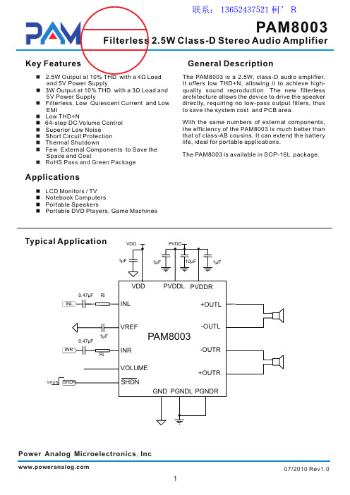
Typical Application VDD
PVDD
1µF
1µF
10µF
1µF
7106中文资料

UTC 7106 CMOS ICUTC UNISONIC TECHNOLOGIES CO., LTD.3QW-R502-018,BABSOLUTE MAXIMUM RATINGS (Ta=25℃) PARAMETER SYMBOL RATINGS UNITSupply Voltage (V+ ~ V-)V DD 15 VAnalog Input Voltage (Either Input) (Note 1) V I,ANG V+ ~ V- V Reference Input Voltage (Either Input) V I,REF V+ ~ V- VOperating Temperature RangeT OP 0 ~ +70℃THERMAL INFORMATIONPARAMETER SYMBOLRATINGS UNITThermal Resistance (Tyical, Note 2)DIP-40QFP-44θJA5075(°C/W)Maximum Junction Temperature T J 150 °CMaximum Storage Temperature Range T STG -65 ~ +150 °C Maximum Lead Temperature (Soldering 10s) (QFP-44 only) T LOAD 300 °C Note 1: Input voltages may exceed the supply voltages provided the input current is limited to ±100μA.Note 2: θJA is measured with the component mounted on a low effective thermal conductivity test board in free air.See Tech Brief TB379 for details.ELECTRICAL CHARACTERISTICS (Note 3)PARAMETER SYMBOLTEST CONDITIONS MIN TYP MAX UNIT SYSTEM PERFORMANCE Zero Input ReadingR ZV IN =0.0V, Full Scale=200mV-000.0±000.0 +000.0DigitalReading Ratiometric Reading R R V IN =V REF , V REF =100mV 999 999/1000 1000DigitalReadingRollover Error E R -V IN =+V IN ≒200mVDifference in Reading forEqual Positive and Negative Inputs Near Full Scale ±0.2 ±1 CountsLinearity L Full Scale=200mV or Full Scale=2V Maximum Devi-ation from Best Straight Line Fit (Note 5)±0.2±1 CountsCommon Mode Rejection Ratio CMRR V CM =1V,V IN =0V,Full Scale=200mV(Note 5) 50μV/V Noise V N V IN =0V,Full Scale=200mV(Peak-To-Peak Value Not Exceeded 95% of Time)15μV Leakage Current Input I L V IN =0(Note 5) 1 10 pAZero Reading Drift D ZR V IN =0, 0℃ ~ 70℃ (Note 5) 0.2 1 μV/℃ Scale Factor TemperatureCoefficientΦT,S V IN =199mV, 0℃ ~ 70℃, (Ext.Ref.0ppm/℃) (Note 5) 1 5ppm/℃ End Power Supply Character V+Supply CurrentI EPV IN =1.0 1.8 mACOMMON Pin Analog CommonVoltage V COM 25k Ω Between Common and Positive Supply (With Respect to +Supply) 2.4 3.0 3.2 VUTC 7106 CMOS ICUTC UNISONIC TECHNOLOGIES CO., LTD.4QW-R502-018,BPARAMETER SYMBOLTEST CONDITIONS MIN TYP MAX UNIT Temperature Coefficient of Analog CommonΦT,A25k Ω Between Common and Positive Supply (With Respect to +Supply)80ppm/℃ DISPLAY DRIVERPeak-To-Peak Segment Drive VoltagePeak-To-Peak Backplane Drive VoltageV D,PP V+ ~ V-=9V(Note 4) 4 5.5 6 V Note 3: Unless otherwise noted, specifications apply to the UTC 7106 at T a =25℃, f CLOCK =48kHz, UTC 7106 is tested in the circuit of Figure 1.Note 4: Back plane drive is in phase with segment drive for”off”segment,180 degrees out of phase for”on” segment .Frequency is 20 times conversion rate. Average DC component is less than 50mV. Note 5: Not tested, guaranteed by design.TYPICAL APPLICATIONS AND TEST CIRCUITS(LCD DISPLAY COMPONENTS SELECTED FOR 200mV FULL SCALE)C1=0.1μF C2=0.47μF C3=0.22μF C4=100pF C5=0.02μF R1=24k ΩR2=47k ΩR3=91k ΩR4=1k ΩR5=1M ΩDESIGN INFORMATION SUMMARY SHEET*OSCILLATOR FREQUENCY fosc=0.45/RCC OSC >50pF, R OSC >50k Ω f OSC (Typ)=48kHz*OSCILLATOR PERIOD t OSC =RC/0.45*INTEGRATION CLOCK FREQUENCYUTC 7106CMOS IC f CLOCK=f OSC/4*INTEGRATION PERIODt INT=1000×(4/f OSC)*60/50Hz REJECTION CRITERIONt INT/t60Hz or t INT/t50Hz=Integer*OPTIMUM INTEGRATION CURRENTI INT=4μA*FULL SCALE ANALOG INPUT VOLTAGEV INFS (Typ)=200mV or 2V*INTEGRATE ESISTORR INT= V INFS/ I INT*INTEGRATE CAPACITORC INT=(t INT)(I INT)/ V INT*INTEGRATOR OUTPUT VOLTAGE SWINGV INT=(t INT)(I INT)/ C INT*VINT MAXIMUM SWING(V- + 0.5V)<V INT<(V+ - 0.5V), V INT (Typ)=2V*DISPLAY COUNTCOUNT=1000×V IN/V REF*CONVERSION CYCLEt CYC=t CLOCK×4000t CYC=t OSC×16,000When f OSC=48kHz, t CYC=333ms*COMMON MODE INPUT VOLTAGE(V- + 1V)<V IN<(V+ - 0.5V)*AUTO-ZERO CAPACITOR0.01μF<C AZ<1μF*REFERENCE CAPACITOR0.1μF<C REF<1μF*V COMBiased between Vi and V-*V COM≒V+ - 2.8VRegulation lost when V+ to V- <≒6.8VIf V COM is externally pulled down to (V+ to V-)/2, the V COM circuit will turn off.*POWER SUPPLY: SINGLE 9VV+ - V- =9VUTC UNISONIC TECHNOLOGIES CO., LTD. 5QW-R502-018,BUTC 7106CMOS IC V GND≒V+ - 4.5VDigital supply is generated by internal parts.*DISPLAY: LCDType: Direct drive with digital logic supply amplitude.TYPICAL INTEGRATOR AMPLIFIER OUTPUT WAVEFORM (INT PIN)TOTAL CONVERSION TIME=4000 × t CLOCK=16,000 × toscDETAILED DESCRIPTIONANALOG SECTIONFigure 1 shows the Analog Section for the UTC 7106. Each measurement cycle is divided into three phases. They are(1) auto-zero(A-Z), (2)signal integrate (INT)and (3)de-integrate(DE).AUTO-ZERO PHASEDuring auto-zero three things happen. First, input high and low are disconnected from the pins and internally shorted to analog COMMON. Second, the reference capacitor is charged to the reference voltage. Third, a feedback loop is closed around the system to charge the auto-zero capacitor C AZ to compensate for offset voltages in the buffer amplifier, integrator, and comparator. Since the comparator is included in the loop, the A-Z accuracy is limited only by the noise of the system. In any case. the offset referred to the input is less than 10μV.SIGNAL INTEGRATE PHASEDuring signal integrate, the auto-zero loop is opened, the internal short is removed, and the internal input high and low are connected to the external pins. The converter then integrates the differential voltage between IN HI and IN LO for a fixed time. This differential voltage can be within a wide common mode range: up to 1V from either supply. if, on the other hand, the input signal has no return with respect to the converter power supply, IN LO can be tied to analog COMMON to establish the correct common mode voltage. At the end of this phase, the polarity of the integrated signal is determined.DE-INTEGRATE PHASEThe final phase is de-integrate, or reference integrate. Input low is internally connected to analog COMMON and input high is connected across the previously charged reference capacitor. Circuitry within the chip ensures that the capacitor will be connected with the correct polarity to cause the integrator output to return to zero. The time required for the output to return to zero is proportional to the input signal. Specifically the digital reading displayed is: DISPLAY COUNT=1000( V IN/ V REF ).DIFFERENTIAL INPUTThe input can accept differential voltages anywhere within the common mode range of the input amplifier, or specifically from 0.5V below the positive supply to 1V above the negative supply. In this range, the system has a CMRR of 86dB typical. However, care must be exercised to assure the integrator output does not saturate. A worst UTC UNISONIC TECHNOLOGIES CO., LTD. 6QW-R502-018,BUTC 7106 CMOS ICUTC UNISONIC TECHNOLOGIES CO., LTD.7QW-R502-018,Bcase condition would be a large positive common mode voltage with a near full scale negative differential input voltage. The negative input signal drives the integrator positive when most of its swing has been used up by the positive common mode voltage. For these critical applications the integrator output swing can be reduced to less than the recommended 2V full scale swing with little loss of accuracy. The integrator output can swing to within 0.3V of either supply without loss of linearity.DIFFERENTIAL REFERENCEThe reference voltage can be generated anywhere within the power supply voltage of the converter. The main source of common mode error is a roll-over voltage caused by the reference capacitor losing or gaining charge to stray capacity on its nodes. If there is a large common mode voltage, the reference capacitor can gain charge (increase voltage) when called up to de-integrate a positive signal but lose charge (decrease voltage) when called up to de-integrate a negative input signal. This difference in reference for positive or negative input voltage will give a roll-over error. However, by selecting the reference capacitor such that it is large enough in comparison to the straycapacitance, this error can be held to less than 0.5 count worst case. (See Component Value Selection)COMMONIN LOFIGURE 1. ANALOG SECTIONIN HIANALOG COMMONThis pin is included primarily to set the common mode voltage for battery operation (UTC 7106) or for any system where the input signals are floating with respect to the power supply. The COMMON pin sets a voltage that is approximately 2.8V more negative than the positive supply. This is selected to give a minimum end-of-life battery voltage of about 6V. However, analog COMMON has some of the attributes of a reference voltage. When the total supply voltage is large enough to cause the zener to regulate(>7V), the COMMON voltage will have a low voltage coefficient (0.001%/V), low output impedance (≒15Ω), and a temperature coefficient typically less than 80ppm/℃. The UTC 7106, with its negligible dissipation, suffers from none of these problems. In either case, an external reference can easily be added, as shown in Figure 1.Analog COMMON is also used as the input low return during auto-zero and de-integrate. If IN LO is different from analog COMMON, a common mode voltage exists in the system and is taken care of by the excellent CMRR of the converter. However, in some applications IN LO will be set at a fixed known voltage(power supply common for instance).In this application, analog COMMON should be tied to the same point, thus removing the common mode voltage from the converter. The same holds true for the reference voltage. If reference can be conveniently tied to analog COMMON, it should be since this removes the common mode voltage from the reference system.Within the IC, analog COMMON is tied to an N-Channel FET that can sink approximately 30mA of current to hold the voltage 2.8V below the positive supply (when a load is trying to pull the common line positive). However, there isUTC 7106 CMOS ICUTC UNISONIC TECHNOLOGIES CO., LTD.8QW-R502-018,Bonly 10μA of source current, so COMMON may easily be tied to a more negative voltage thus overriding the internalreference.FIGURE 2B.FIGURE 2A.FIGURE 2. USING AN EXTERNAL REFERENCETESTThe TEST pin serves two function. On the UTC 7106 it is coupled to the internally generated digital supply through a 500Ω resistor. Thus it can be used as the negative supply for externally generated segment drivers such as decimal points or any other presentation the user may want to include on the LCD display. Figures 3 and 4 show such an application. No more than a 1mA load should be applied.The second function is a “lamp test”. When TEST is pulled high (to V+) all segments will be turned on and the display should read ”1888”. The TEST pin will sink about 15mA under these conditions.CAUTION: In the lamp test mode, the segments have a constant DC voltage (no square-wave) . This may burn the LCD display if maintained for extended periods.FIGURE 3. SIMPLE INVERTER FOR FIXED DECIMAL POINTTO LCD DECIMAL POINTSFIGURE 4. EXCLUSIVE "OR" GATE FORDECIMAL POINT DRIVEDIGITAL SECTIONFigure 5 show the digital section for the UTC 7106, respectively. In the UTC 7106, an internal digital ground is generated from a 6V Zener diode and a large P-Channel source follower. This supply is made stiff to absorb the relative large capacitive currents when the back plane(BP) voltage is switchied. The BP frequency is the clock frequency divided by 800. For three readings/sec, this is a 60Hz square wave with a nominal amplitude of 5V. TheUTC 7106 CMOS ICUTC UNISONIC TECHNOLOGIES CO., LTD.9QW-R502-018,Bsegments are driven at the same frequency and amplitude and are in phase with BP when OFF, but out of phase when ON. In all cases negligible DC voltage exists across the segments.FIGURE 5. DIGITAL SECTIONTESTV-V+SYSTEM TIMINGFigure 6 shows the clocking arrangement used in the UTC 7106. Two basic clocking arrangements can be used: 1. Figure 6A. An external oscillator connected to pin 40. 2. Figure 6B. An R-C oscillator using all three pins.The oscillator frequency is divided by four before it clocks the decade counters. It is then further divided to form the three convert-cycle phases. These are signal integrate (1000 counts), reference de-integrate(0 to 2000 counts) and auto-zero(1000 ~ 3000 counts). For signals less than full scale. auto-zero gets the unused portion of reference de-integrate. This makes a complete measure cycle of 4,000 counts (16,000 clock pulses) independent of input voltage. For three readings/second, an oscillator frequency of 48kHz would be used.To achieve maximum rejection of 60Hz pickup, the signal integrate cycle should be a multiple of 60Hz. Oscillator frequencies of 240kHz, 120kHz, 80kHz, 60kHz, 48kHz, 40kHz, 33 1/3kHz, etc should be selected. For 50Hz rejection, Oscillator frequencies of 200kHz, 100kHz, 66 2/3kHz, 50kHz, 40kHz, etc would be suitable. Note that 40kHz (2.5 readings/second) will reject both 50Hz and 60Hz (also 400Hz and 440Hz).UTC 7106 CMOS ICUTC UNISONIC TECHNOLOGIES CO., LTD.10QW-R502-018,BFIGURE 6AFIGURE 6BFIGURE 6. CLOCK CIRCUITSCOMPONENT VALUE SELECTION Integrating ResistorBoth the buffer amplifier and the integrator have a class A output stage with 100μA of quiescent current. They can supply 4μA of drive current with negligible nonlinearity. The integrating resistor should be large enough toremain in this very linear region over the input voltage range, but small enough that undue leakage requirements are not placed on the PC board. For 2V full scale, 470k Ω is near optimum and similarly a 47k Ω for a 200mV scale.Integrating CapacitorThe integrating capacitor should be selected to give the maximum voltage swing that ensures tolerance buildup will not saturate the integrator swing(approximately. 0.3V from either supply).In the UTC 7106, when the analogCOMMON is used as a reference, a nominal+2V fullscale integrator swing is fine. For three readings/second (48kHz clock) nominal values for C INT are 0.22μF and 0.10μF, respectively. Of course, if different oscillator frequencies are used, these values should be changed in inverse proportion to maintain the same output swing.An additional requirement of the integrating capacitor is that it must have a low dielectric absorptiont to prevent roll-over errors. While other types of capacitors are adequate for this application, polypropylene capacitors give undetectable errors at reasonable cost.Auto-Zero CapacitorThe size of the auto-zero capacitor has some influence on the noise of the system. For 200mV full scale where noise is very important, a 0.47μF capacitor is recommended. On the 2V scale, a 0.047μF capacitor increases the speed of recovery from overload and is adequate for noise on this scale.Reference CapacitorA 0.1μF capacitor gives good results in most applications. However, where a large common mode voltage exists (i.e.,the REF LO pin is not at analog COMMON)and a 200mV scale is used, a larger value is required to prevent roll-ovre error. Generally 1μF will hold the roll-over error to 0.5 count in this instance.Oscillator ComponentsFor all ranges of frequency a 91k Ω resistor is recommended and the capacitor is selected from the equation: f= 0.45/RC For 48kHz Clock (3 Readings/sec), C=100pF.Reference VoltageThe analog input required to generate full scale output (2000 counts) is: V IN =2V REF .Thus, for the 200mV and 2V scale, V REF should equal 100mV and 1V, respectively.However,in many applications where the A/D is connected to a transducer, there will exist a scale factor other than unity between the input voltage and the digital reading. For instance, in a weighing system, the designer might like to have a full scale reading when the voltage from theUTC 7106 CMOS ICUTC UNISONIC TECHNOLOGIES CO., LTD.11QW-R502-018,Btransducer is 0.662V. Instead of dividing the input down to 200mV, the designer should use the input voltage directly and select V REF =0.341V. Suitable values for integrating resistor and capacitor would be 120k Ω and 0.22μF. This makes the system slightly quieter and also avoids a divider network on the input.TYPICAL APPICATIONSThe UTC 7106 may be used in a wide variety of configurations. The circuits which follow show some of the possibilities, and serve to illustrate the exceptional versatility of these A/D converters.9V INValues shown are for 200mV full scale,3 readings/sec.,floating supply voltage(9V battery).FIGURE 7. USING THE INTERNAL REFERENCEUTC 7106 CMOS ICUTC UNISONIC TECHNOLOGIES CO., LTD.12QW-R502-018,BTYPICAL APPLICATIONS (Continued)INFIGURE 8. RECOMMENDED COMPONENT VALUES FOR 2V FULL SCALEV-UTC 7106CMOS IC TYPICAL APPLICATIONS (Continued)A sillicon diode-connected transistor has a temperature coefficient of about -2mV/ ℃.Calibration is achieved by placing the sensing transistor in ice water and adjusting thezeroing potentiometer for a 000.0 reading.The sensor should then be placed in boilingwater and the scale-factor potentiometer adjusted for a 100.0 readingFIGURE 9. USED AS A DIGITAL CENTIGRADE THERMOMETER UTC UNISONIC TECHNOLOGIES CO., LTD. 13QW-R502-018,BUTC 7106CMOS IC TYPICAL APPLICATIONS (Continued)CD4077FIGURE 10. CIRCUIT FOR DEVELOPING UNDERRANGE ANDOVERRANGE SIGNAL FROM UTC 7106 OUTPUTSUTC UNISONIC TECHNOLOGIES CO., LTD. 14QW-R502-018,BUTC 7106CMOS IC TYPICAL APPLICATIONS (Continued)Test is used as a common-mode reference level to ensure compatiblity with most op amps.FIGURE 11. AC TO DC CONVERTER WITH UTC 7106UTC UNISONIC TECHNOLOGIES CO., LTD. 15QW-R502-018,B。
SC1132CT-2.5DB中文资料

2
4
6
8
Load Current (A)
3.3 2.9 2.5 1.8
10
SC113X
% Load Regulation 3.3V, 0.3 to 10 Amps
1.0
0.5
0.0
-0.5
-1.0
-1.5
-2.0
0
2
4
6
8
10
Load Current (A)
% Load Regulation 2.9V, 0.3 to 10 Amps
R2
C10
0.01uF
C9 1000uF +
Vout (LIN)
12V IN
C11 0.1uF
Revision 1, December 2000
1
SC113X
POWER MANAGEMENT Absolute Maximum Ratings
Operating Temperature Junction Operating Temperature Storage Temperature Lead Soldering Temperature Thermal Resistance, Junction to Case Thermal Resistance, Junction to Ambient
Typ VOUT
VOUT 1.250
1.250 0.005 0.035
0.05 0.2
1
1.1 10
0.004
Max +1% +2% 1.262 1.275 0.2 0.2
0.3 0.4
1.3 13 0.02
Units V V %
SPF-5043Z-EVB1中文资料
21.0
Output Third Order Intercept Point
33.0
35.0
Noise Figure
0.80
0.80
Input Return Loss
-16.0
-17.5
Output Return Loss
-17.5
-16.5
Reverse Isolation
-23.5
-19.0
Device Operating Voltage
Condition
RF MICRO DEVICES®, RFMD®, Optimum Technology Matching®, Enabling Wireless Connectivity™, PowerStar®, POLARIS™ TOTAL RADIO™ and UltimateBlue™ are trademarks of RFMD, LLC. BLUETOOTH is a trademark owned by Bluetooth SIG, Inc., U.S.A. and licensed for use by RFMD. All other trade names, trademarks and registered trademarks are the property of their respective owners. ©2006, RF Micro Devices, Inc.
元器件交易网
Preliminary SPF-5043Z
50MHz to 4000 MHz, GaAs pHEMT Low Noise MMIC Amplifier
SPF-5043Z
50MHz to 4000MHz, GaAs pHEMT LOW NOISE MMIC AMPLIFIER
RF5110中文资料
Product DescriptionOrdering InformationTypical Applications FeaturesFunctional Block DiagramRF Micro Devices, Inc.7628 Thorndike RoadGreensboro, NC 27409, USA Tel (336) 664 1233Fax (336) 664 0454Optimum Technology Matching® AppliedSi BJT GaAs MESFET GaAs HBTSi Bi-CMOS SiGe HBTSi CMOS InGaP/HBTGaN HEMTSiGe Bi-CMOS16151413121110912345678VCC1GND1RF IN GND2V C C 2V C C 2N C2f 0RF OUTRF OUT RF OUT RF OUT V C C N CA P C 1A P C 23V GSM POWER AMPLIFIER•3V GSM Cellular Handsets•3V Dual-Band/Triple-Band Handsets •GPRS Compatible •Commercial and Consumer Systems •Portable Battery-Powered EquipmentThe RF5110 is a high-power, high-efficiency power ampli-fier module offering high performance in GSM OR GPRS applications. The device is manufactured on an advanced GaAs HBT process, and has been designed for use as the final RF amplifier in GSM hand-held digital cellular equipment and other applications in the 800MHz to 950MHz band. On-board power control provides over 70dB of control range with an analog voltage input, and provides power down with a logic “low” for standby opera-tion. The device is self-contained with 50Ω input and the output can be easily matched to obtain optimum power and efficiency characteristics. The RF5110 can be used together with the RF5111 for dual-band operation. The device is packaged in an ultra-small 3mmx3mmx1mm plastic package, minimizing the required board space.•Single 2.7V to 4.8V Supply Voltage •+36dBm Output Power at 3.5V •32dB Gain with Analog Gain Control •57% Efficiency•800MHz to 950MHz Operation •Supports GSM and E-GSMRF51103V GSM Power AmplifierRF5110 PCBAFully Assembled Evaluation BoardShaded lead is pin 1.Package Style: QFN, 16-Pin, 3x39Absolute Maximum RatingsParameterRatingUnitSupply Voltage-0.5 to +6.0V DC Power Control Voltage (V APC1,2)-0.5 to +3.0V DC Supply Current 2400mA Input RF Power+13dBm Duty Cycle at Max Power 50%Output Load VSWR10:1Operating Case Temperature -40 to +85°C Storage Temperature-55 to +150°CParameterSpecification Unit ConditionMin.Typ.Max.OverallTemp=25°C, V CC =3.6V , V APC1,2=2.8V,P IN =+4.5dBm, Freq=880MHz to 915MHz, 37.5% Duty Cycle, pulse width=1731µs Operating Frequency Range 880 to 915MHz See evaluation board schematic.Usable Frequency Range 800 to 950MHz Using different evaluation board tune.Maximum Output Power 33.834.5dBm Temp=25°C, V CC =3.6V , V APC1,2=2.8V 33.1dBm Temp=+60°C, V CC =3.3V , V APC1,2=2.8V T otal Efficiency5057%At P OUT,MAX , V CC =3.6V 12%P OUT =+20dBm 5%P OUT =+10dBmInput Power for Max Output +4.5+7.0+9.5dBm Output Noise Power-72dBmRBW=100kHz, 925MHz to 935MHz, P OUT,MIN <P OUT <P OUT,MAX ,P IN,MIN <P IN <P IN,MAX , V CC =3.3V to 5.0V -81dBmRBW=100kHz, 935MHz to 960MHz, P OUT,MIN <P OUT <P OUT,MAX ,P IN,MIN <P IN <P IN,MAX , V CC =3.3V to 5.0V Forward Isolation -22dBm V APC1,2=0.3V, P IN =+9.5dBm Second Harmonic -20-7dBm P IN =+9.5dBm Third Harmonic-25-7dBm P IN =+9.5dBmAll Other Non-HarmonicSpurious -36dBm Input Impedance50ΩOptimum Source Impedance 40+j10ΩFor best noise performanceInput VSWR 2.5:1P OUT,MAX -5dB<P OUT <P OUT,MAX 4:1P OUT <P OUT,MAX -5dBOutput Load VSWRStability8:1Spurious<-36dBm, V APC1,2=0.3V to 2.6V, RBW=100kHz Ruggedness10:1No damageOutput Load Impedance2.6-j1.5ΩLoad Impedance presented at RF OUT pad Power Control V APC1 V APC2Power Control “ON” 2.6V Maximum P OUT , Voltage supplied to the inputPower Control “OFF”0.20.5V Minimum P OUT , Voltage supplied to the input Power Control Range 75dB V APC1,2=0.2V to 2.6VGain Control Slope 5100150dB/V P OUT =-10dBm to +35dBm APC Input Capacitance 10pF DC to 2MHz APC Input Current 4.55mA V APC1,2=2.8V 25µA V APC1,2=0VT urn On/Off Time100nsV APC1,2=0 to 2.8VESD sensitive device.RF Micro Devices believes the furnished information is correct and accurate at the time of this printing. However, RF Micro Devices reserves the right to make changes to its products without notice. RF Micro Devices does not assume responsibility for the use of the described product(s).ParameterSpecificationUnit Condition Min.Typ.Max.Power SupplyPower Supply Voltage 3.5V Specifications2.7 4.8V Nominal operating limits, P OUT<+35dBm5.5V With maximum output load VSWR 6:1,P OUT<+35dBmPower Supply Current2A DC Current at P OUT,MAX15200335mA Idle Current, P IN<-30dBm110µA P IN<-30dBm, V APC1,2=0.2V110µA P IN<-30dBm, V APC1,2=0.2V, Temp=+85°CTheory of Operation and Application InformationThe RF5110 is a three-stage device with 32 dB gain at full power. Therefore, the drive required to fully saturate the out-put is +3dBm. Based upon HBT (Heterojunction Bipolar T ransistor) technology, the part requires only a single positive 3V supply to operate to full specification. Power control is provided through a single pin interface, with a separate Power Down control pin. The final stage ground is achieved through the large pad in the middle of the backside of the package. First and second stage grounds are brought out through separate ground pins for isolation from the output. These grounds should be connected directly with vias to the PCB ground plane, and not connected with the output ground to form a so called “local ground plane” on the top layer of the PCB. The output is brought out through the wide output pad, and forms the RF output signal path.The amplifier operates in near Class C bias mode. The final stage is “deep AB”, meaning the quiescent current is very low. As the RF drive is increased, the final stage self-biases, causing the bias point to shift up and, at full power, draws about 2000mA. The optimum load for the output stage is approximately 2.6Ω. This is the load at the output collector, and is created by the series inductance formed by the output bond wires, vias, and microstrip, and 2 shunt capacitors exter-nal to the part. The optimum load impedance at the RF Output pad is 2.6-j1.5Ω. With this match, a 50Ω terminal imped-ance is achieved. The input is internally matched to 50Ω with just a blocking capacitor needed. This data sheet defines the configuration for GSM operation.The input is DC coupled; thus, a blocking cap must be inserted in series. Also, the first stage bias may be adjusted by a resistive divider with high value resistors on this pin to V PC and ground. For nominal operation, however, no external adjustment is necessary as internal resistors set the bias point optimally.VCC1 and VCC2 provide supply voltage to the first and second stage, as well as provides some frequency selectivity to tune to the operating band. Essentially, the bias is fed to this pin through a short microstrip. A bypass capacitor sets the inductance seen by the part, so placement of the bypass cap can affect the frequency of the gain peak. This supply should be bypassed individually with 100pF capacitors before being combined with V CC for the output stage to prevent feedback and oscillations.The RF OUT pin provides the output power. Bias for the final stage is fed to this output line, and the feed must be capa-ble of supporting the approximately 2A of current required. Care should be taken to keep the losses low in the bias feed and output components. A narrow microstrip line is recommended because DC losses in a bias choke will degrade effi-ciency and power.While the part is safe under CW operation, maximum power and reliability will be achieved under pulsed conditions. The data shown in this data sheet is based on a 12.5% duty cycle and a 600µs pulse, unless specified otherwise.The part will operate over a 3.0V to 5.0V range. Under nominal conditions, the power at 3.5V will be greater than +34.5dBm at +90°C. As the voltage is increased, however, the output power will increase. Thus, in a system design, the ALC (Automatic Level Control) Loop will back down the power to the desired level. This must occur during operation, or the device may be damaged from too much power dissipation. At 5.0V, over +38dBm may be produced; however, this level of power is not recommended, and can cause damage to the device.The HBT breakdown voltage is >20V, so there are no issue with overvoltage. However, under worst-case conditions, with the RF drive at full power during transmit, and the output VSWR extremely high, a low load impedance at the collector of the output transistors can cause currents much higher than normal. Due to the bipolar nature of the devices, there is no limitation on the amount of current de device will sink, and the safe current densities could be exceeded.High current conditions are potentially dangerous to any RF device. High currents lead to high channel temperatures and may force early failures. The RF5110 includes temperature compensation circuits in the bias network to stabilize the RF transistors, thus limiting the current through the amplifier and protecting the devices from damage. The same mechanism works to compensate the currents due to ambient temperature variations.T o avoid excessively high currents it is important to control the V APC when operating at supply voltages higher than 4.0V, such that the maximum output power is not exceeded.Internal SchematicRF INVCC1PKG BASE GND2VCC2RF OUTPKG BASEAPC1Evaluation Board Schematic GSM850 Lumped ElementJ1 RF INJ2 VCCVCCJ3 VAPCEvaluation Board Schematic GSM900 Lumped ElementJ1RF INJ3VAPCJ2RF OUTC23 and C27 share the same pad.Evaluation Board LayoutBoard Size 2.0” x 2.0”Board Thickness 0.032”; Board Material FR-4; Multi-LayerTypical Test SetupNotes about testing the RF5110The test setup shown above includes two attenuators. The 3dB pad at the input is to minimize the effect on the signal generator as a result of switching the input impedance of the PA. When V APC is switched quickly, the resulting input impedance change can cause the signal generator to vary its output signal, either in output level or in frequency. Instead of an attenuator an isolator may also be used. The attenuator at the output is to prevent damage to the spectrum ana-lyzer, and should be sized accordingly to handle the power.It is important not to exceed the rated supply current and output power. When testing the device at higher than nominal supply voltage, the V APC should be adjusted to avoid the output power exceeding +36dBm. During load-pull testing at the output it is important to monitor the forward power through a directional coupler. The forward power should not exceed +36dBm, and V APC needs to be adjusted accordingly. This simulates the behavior for the power control loop. T o avoid damage, it is recommended to set the power supply to limit the current during the burst not to exceed the maximum current rating.Buffer x1 OpAmpA buffer amplifier is recommended because the current into the V APC changes with voltage. As an alternative, the voltage may be monitored with an oscilloscope.RF5110PCB Design RequirementsPCB Surface FinishThe PCB surface finish used for RFMD’s qualification process is electroless nickel, immersion gold. T ypical thickness is 3µinch to 8µinch gold over 180µinch nickel.PCB Land Pattern RecommendationPCB land patterns for PFMD components are based on IPC-7351 standards and RFMD empirical data. The pad pattern shown has been developed and tested for optimized assembly at RFMD. The PCB land pattern has been developed to accommodate lead and package tolerances. Since surface mount processes vary from company to company, careful process development is recommended.PCB Metal Land PatternA = 0.64 x 0.28 (mm) Typ.B = 0.28 x 0.64 (mm) Typ.C = 1.50 (mm) Sq.Dimensions in mm.Figure 1. PCB Metal Land Pattern (Top View)RF5110PCB Solder Mask PatternLiquid Photo-Imageable (LPI) solder mask is recommended. The solder mask footprint will match what is shown for the PCB metal land pattern with a 2mil to 3mil expansion to accommodate solder mask registration clearance around all pads. The center-grounding pad shall also have a solder mask clearance. Expansion of the pads to create solder mask clearance can be provided in the master data or requested from the PCB fabrication supplier.A = 0.74 x 0.38 (mm) Typ.B = 0.38 x 0.74 (mm) Typ.C = 1.60 (mm) Sq.Dimensions in mm.Figure 2. PCB Solder Mask Pattern (Top View)Thermal Pad and Via DesignThe PCB land pattern has been designed with a thermal pad that matches the die paddle size on the bottom of the device.Thermal vias are required in the PCB layout to effectively conduct heat away from the package. The via pattern has been designed to address thermal, power dissipation and electrical requirements of the device as well as accommodating routing strategies.The via pattern used for the RFMD qualification is based on thru-hole vias with 0.203mm to 0.330mm finished hole size on a 0.5mm to 1.2mm grid pattern with 0.025mm plating on via walls. If micro vias are used in a design, it is suggested that the quantity of vias be increased by a 4:1 ratio to achieve similar results.。
AHigh-Gain,Low-PowerCMOSOpAmpUsing
A High-Gain,Low-Power CMOS Op Amp UsingComposite Cascode StagesDavid er,Fellow IEEE,Donald er,and Rishi Pratap Singh Department of Electrical and Computer Engineering Brigham Young UniversityProvo,UT84602Email:comer@June1,2010Abstract–This work demonstrates that the com-posite cascode differential stage,operating in the subthreshold region,can form the basis of a high-gain(110dB),low-power op amp(27.8µW).The circuit can be fabricated without adding a compen-sation capacitance.Advantages of this architecture include high voltage gain,low harmonic distortion, low quiescent current and power,and small chip area.These advantages suggest that this design might be well-suited for low-power instrumentation applications requiring multiple amplifiers as often found in biomedical applications.I.IntroductionIn recent years,an area of increasing interest is that of biomedical instrumentation amplifiers[1],[2].These ap-plications typically require high gain,low power,low fre-quency,amplifiers that occupy minimal chip real estate. This work discusses the subthreshold operation of compos-ite cascode stages to achieve advantages such as high volt-age gain[3],low nonlinear distortion[1],[4]low noise[1], low power,low chip area,and low bandwidth.Although low bandwidth is often considered a shortcoming,in this case,it can eliminate the need for a compensation capaci-tor to achieve stable operation in the presence of feedback. Required chip area is reduced by deleting this capacitance.II.The Classical Op Amp ArchitectureThefirst generation,bipolar junction transistor(BJT), general purpose,integrated circuit(IC)op amp of1964 was designed to have a high voltage gain differential input stage,a moderately high voltage gain second stage,and a low voltage gain/high current gain third stage that acts as a buffer[5].Thefirst two stages develop the high overall voltage gain needed for the op amp circuit.This config-uration,sometimes referred to as the Widlar architecture, has continued in the design of op amps,for both BJT and CMOS devices.These early IC op amps required an external capacitance or an external RC combination to compensate the op amp [5].This compensating network was placed between the output of thefirst stage and ground.The capacitance needed was considerably larger than could be integrated on the chip.In the next generation of IC op amps,appear-ing in1968,the Miller effect was used in conjunction with the second stage to reflect a large capacitance to the output of thefirst stage for compensation[6].Although this Miller capacitance eliminates the need for an external compensating capacitance,a few negative fac-tors must now be considered.Thefirst is the feedthrough that takes place in the second stage.The signal applied to the input of the second stage now has two paths to the third stage;one is through the amplifier,but a second sig-nal feeds through the capacitance that bridges the input and output nodes of the second stage.In most applica-tions,the feedthrough signal is negligible compared to the amplified signal and can be ignored.In a small number of applications,especially digital signals with small rise times, the feedthrough signal can be troublesome.An additional resistance in series with the compensation capacitance[8] can be added to minimize feedthrough.A second factor to consider is one that involves the analy-sis or design of the op amp.Bridging the input and output nodes of the second stage results in a phenomenon known as “pole splitting”.While the objective of lowering the pole or3-dB frequency of thefirst stage is achieved,the pole of the second stage is moved to a higher frequency.This effect is more pronounced in BJT circuits than in CMOS circuits,but must often be considered in the design with either device[7].Pole splitting is advantageous in achiev-ing a higher frequency design,but requires a capacitance and a resistance for proper compensation and,thus,adds complexity to the design.A third factor that can be significant in single-chip ampli-fier arrays is the need for additional chip area required by the compensation capacitance and resistance.Each com-pensating capacitor may have a value of tens of pF and occupy a significant chip area.The resistance is often im-plemented by a MOSFET in the triode region and requires little extra area.As CMOS circuits grew in popularity,the BJT architec-ture was applied to CMOS designs.The low transconduc-tance of the MOS device compared to that of the BJT has resulted in several departures from the classical architec-ture for comparable performance of the CMOS op amp.IfVV inFigure1:Single-ended composite cascode gain stage.only two stages of voltage amplification are used,voltage gain of the op amp is relatively low[8].Other implementa-tions add more gain stages to increase the overall gain,but become correspondingly more complex[9].This work increases the CMOS op amp gain to BJT-like levels by using the composite cascode stage operating in the subthreshold region.In addition,the parasitic capacitance at the output of thefirst stage is used to compensate the op amp.Not only are the effects of feedthrough and pole splitting minimized in this way,a great deal of chip area is conserved by eliminating the compensation capacitor.Be-cause of the low dc current required by the differential input stage,dc power consumption can also be minimized.Op-eration in the weak inversion region can also lead to lower harmonic distortion than strong inversion operation[4].III.Operation of MOS Devices in Weak InversionAn earlier work[4]demonstrated the high gain that can be obtained with the composite cascode stage operating in the weak inversion region and suggested the use of this stage for thefirst differential stage of a CMOS op amp. This work also suggested that the resulting lower corner frequency of thefirst stage would result in a smaller com-pensation capacitor.In another work[10],it was suggested that voltage gains exceeding10,000V/V per stage could be achieved by combining operation in the weak or moderate inversion region with the composite cascode configuration of Fig. 1.Aspect ratios are chosen to operate the device M2in the subthreshold region while M1operates in the moderate or strong inversion region.Both devices are in the active region.The subthreshold drain current of device M2leads to a large output resistance,resulting in a very high voltage gain.Devices M3and M4provide the compos-ite cascode load for this device which also exhibits a large output resistance.This concept was implemented[3]in a high gain(ap-proximately120dB)CMOS op amp that used the Widlar architecture.In that work,the overall voltage gain was3.62uAFigure2:Composite cascode op amp. apportioned almost equally between thefirst and second stage.Both of these stages have high gain(≈1000V/V) and moderate bandwidth.The circuit for this op amp is shown in Fig. 2.Fabrication of the op amp[3]demon-strated that sufficient gain can be obtained with CMOS composite cascode stages to implement a high gain op amp in the classical Widlar architecture.It also demonstrated that the compensation capacitance can be minimized with this approach,requiring a3.5pF value for the op amp.IV.An Op Amp with no Compensation Capacitance Rather than designing the op amp with a high-gain,mod-erate bandwidthfirst stage and then degrading bandwidth with a compensating capacitor,the premise of this work is to create a very high-gain,very low bandwidthfirst stage. This is done by using the composite cascode differential stage shown in Fig.3.P-channel input devices,M1-M4, are used for the differential pair while the current mirror load is implemented with devices M5-M8.Source followers are inserted between the input signal and the differential stage to act as dc voltage level shifters.The scaling of the devices and the tail current are selected to place devices M3 and M4along with M5and M6in the subthreshold region. This significantly increases the drain to source resistances of these devices.In addition,the load impedances of de-vices M3and M4are further increased due to the source degeneration provided by devices M1and M2.Devices M7 and M8provide source degeneration for devices M5and M6 as well.With the high impedance loads of M1and M3,the gain increases and the bandwidth decreases due to the parasitic capacitance at the output of thisfirst gain stage.This differential stage is similar to that of Fig.2[3],however, the drain current has been decreased and scaling has been changed from that circuit to achieve the proper quiescent current to lead to the increased voltage gain and decreased bandwidth.This high voltage gain stage is followed by an output stage consisting of a source follower(M19)that also acts as a level shifter and the output amplifier consisting of M20andFigure 3:Op amp without added compensation capac-itor.M21.The first stage is designed to achieve a voltage gain of tens of thousands to hundreds of thousands along with a band-width of a few Hertz.The output stage is designed to have a gain between 1and 10V/V with a relatively high band-width.With a dominant pole of a few Hertz,the phase margin of the circuit should be acceptable even in the worst-case,unity gain feedback configuration.No additional com-pensation is required for this amplifier.V.Simulation ResultsOperation of this amplifier was simulated with Cadence using the C5AMI 0.5-µm technology and BSIM3v3device models.The load impedance consisted of a 100-kΩresis-tance in parallel with a 0.5pF capacitance,a heavier load than that presented by the IC lowpass filter that is intended to follow the amplifier stage.For the circuit of Fig.3,the loaded voltage gain of the differential input stage is 43,550V/V and the bandwidth is about 1Hz.The second stage has a loaded voltage gain of 7.46V/V and a bandwidth of about 2.23MHz.The overall voltage gain is 325,000V/V (110dB)while the open loop bandwidth is about 1Hz.The frequency response showing magnitude and phase is plotted in Figs.4and 5.The phase margin is 95◦.For power supply voltages of ±1.5V,the output of the amplifier can swing from -1.25V to +1.35V.In the unity gain configuration,the total harmonic distortion or THD is 0.24%with a 2.4V peak-to-peak output voltage and 1.5%for a 2.6V peak-to-peak output.Table 1summarizes several important parameters for the op amp when driving the capacitor/resistor load.Figure 4:Open loop magnitude response.Figure 5:Open loop phase response.Figure6:Layout of op amp core.Table1Summary of results Open loop gain,dBOpen loop bandwidth,Hz Spectral noise density,HzDC supply current,µANo signal dissipation,µW GBW,kHz。
A 7-GHz 1.8-dB NF CMOS Low-Noise Amplifier
A 7-GHz 1.8-dB NF CMOS Low-Noise AmplifierRyuichi Fujimoto ,Member,IEEE ,Kenji Kojima,and Shoji OtakaAbstract—A 7-GHz low-noise amplifier (LNA)was designed and fabricated using0.25-m CMOS technology.A cascode configuration with a dual-gate MOSFET and shielded pads were adopted to improve the gain and the noise performance.The effects of the dual-gate MOSFET and the shielded pads are discussed quantitatively.An associated gain of 8.9dB,a minimum noise figure of 1.8dB,and an input-referred third-order intercept point of +8.4dBm were obtained at 7GHz.The LNA consumes 6.9mA from a 2.0-V supply voltage.These measured results indi-cate the feasibility of a CMOS LNA employing these techniques for low-noise and high-linearity applications at over 5GHz.Index Terms—Dual-gate MOSFET,intercept point,low-noise amplifier,noise figure,shielded pad,Si substitute.I.I NTRODUCTIONRECENTLY ,wireless communication systems with a car-rier frequency of over 5GHz,such as intelligent trans-port system (ITS)and wireless LAN specified by IEEE 802.11a,have attracted considerable attention.Furthermore,a carrier fre-quency of up to 10GHz is expected to be used for fourth-gen-eration (4G)wireless systems.Thanks to recent advances in CMOS technology,a transitionfrequencyis competitive with that of silicon bipolar junc-tion transistor (Si-BJT)technology.The main noise sources of MOSFETs at high frequency are the thermal noise of channel and gate resistance.The gate resistance is reduced using low-re-sistance salicided gate material and a multifinger gate structure to obtain low noise performance [1],[2],and so the dominant noise source of MOSFETs is the thermal noise of a channel.On the other hand,the main noise sources of Si-BJTs are thermal noise of base resistance and shot noise of the collector current.To reduce base resistance,a large geometry device is needed,but this requires more collector current to keep the samehigh value,which causes more shot noise.To reduce shot noise,a small collector current is needed,but this requires a small geom-etry device to keep the samehighvalue,which causes a large base resistor.So,reducing the thermal noise of the base resis-tance causes large shot noise,and vice versa.Hence,the noise performance of MOSFETs is superior to that of Si-BJTs.CMOS technology is also advantageous for low cost and large-scale in-tegration.Owing to these merits of the CMOS technology,many low-noise amplifiers (LNAs)using CMOS technology have been reported [3]–[7].Considering the demand for systemsManuscript received November 5,2001;revised January 28,2002.R.Fujimoto and S.Otaka are with the Corporate Research and Development Center,Toshiba Corporation,Kawasaki 212-8582,Japan (e-mail:ryuichi.fuji-moto@toshiba.co.jp).K.Kojima is with the SoC Research and Development Center,Toshiba Cor-poration,Semiconductor Company,Yokohama 235-8522,Japan.Publisher Item Identifier S0018-9200(02)05857-2.Fig.1.Si-substrate resistance in CMOS technology.with carrier frequency of over 5GHz,realization of wireless ICs operable at over 5GHz using CMOS technology is desir-able.In this paper,we describe the performance of a 7-GHz LNA with a dual-gate MOSFET,and shielded pads used for its input and output ports.Improvements in low noise performance by adopting the dual-gate MOSFET and the shielded pads are discussed quantitatively.II.D ESIGN C ONSIDERATION FOR L OW N OISE P ERFORMANCE A.Si-Substrate ResistanceAt high frequency,the drain and source of a MOSFET,pads,inductors,and other elements on the Si substrate have resis-tive components due to resistivity of the Si substrate,as shown in Fig.1.This parasitic resistance consumes signal power and generates thermal noise,and thus gain and noise performances of the LNA are degraded.Therefore,circuit techniques are re-quired to reduce the effect of the resistivity due to the Si sub-strate in high-frequency circuit design.Here,two techniques are described for reducing the effect of the resistivity due to the Si substrate.1)Dual-Gate MOSFET:Fig.2shows a schematic diagram of an LNA.A cascode configuration is chosen for improving high-frequency performance.The cascode configuration imple-mented using a dual-gate MOSFET is shown in Fig.3.The area of the parasitic diodes at M1’s drain and M2’s source in Fig.2can be reduced significantly by using the dual-gate MOSFET.Part of the signal current output from M1flows into the parasitic diodes,and this signal current is consumed by the Si-substrate ing the dual-gate MOSFET,this consumption in the Si substrate is reduced due to fact that the area of the par-asitic diodes is small compared to that in the case using two conventional MOSFETs.In accordance with the design rule of MOSFETs,the area of the parasitic diode is reduced by a quarter using the dual-gate MOSFET in our case.Circuit simulation results indicate that the LNA with the dual-gate MOSFET attains 1.2dB higher gain (maximum0018-9200/02$17.00©2002IEEEFig.2.Schematic diagram ofLNA.Fig.3.Dual-gate MOSFETs.available gain)and 0.7dB lower noise figure (minimum noise figure)compared to the values in the case of conventional MOSFETs for M1and M2.2)Shielded Pads:Figs.4and 5show structures and mea-suredcharacteristics for the unshielded conventional pad and the shielded pad,respectively.The conventional pad has a resistive component due to the Si-substrate resistance.There-fore,the measured result in Fig.4shows a capacitive charac-teristic with the parasitic resistance.The resistance value in the equivalent circuit shown in Fig.4is several tens of ohms,and this causes signal power loss and degrades gain and noise char-acteristics of the LNA.This degradation is particularly marked at high frequency of over 5GHz.To avoid such degradation,the shielded pads are used for input and output pads of the LNA [6]–[8].This is because the shielded pads ideally have no resistive component,and so they consume no signal power and generate no noise.The measured result in Fig.5shows the characteristic to be the same as for a pure capacitance.B.Other Factors Effective for Low Noise Performance To reduce gate resistance of dual-gate MOSFET,salicided gate material and multifinger gate structure,shown in Fig.3are adopted.An input matching circuit has a large effect on the noise performance.If the input matching circuit is composedusingFig.4.Structure and measured S 11of the unshielded conventional pad (100MHz–10GHz).Fig.5.Structure and measured S 11of the shielded pad (100MHz–10GHz).on-chip elements withlow values,the power of the input signal is greatly consumed in the resistive part of the on-chip input matching elements.To avoid such consumption,an external input matching circuit is indispensable for achieving very low noise performance.Generally,a signal source impedance which achieves input impedance matching is different from that for the optimum noise figure.To achieve these conditions simultaneously,a degenera-tion inductor L1should be connected to the source of M1[9].III.M EASURED R ESULTSThe LNA with a dual-gate MOSFET was fabricated using0.25-m CMOS technology.The Si-substrate resistivity is the medium value,i.e.,1–2cm,and so these parasitic resistances affect high-frequency circuit performances.Figs.2and 6showFig.6.Die photograph ofLNA.Fig.7.Gains and noise figures of the LNA.a circuit diagram and a die photograph of the LNA,respec-tively.The chip size including the area of the pads is860m610m.The degeneration inductor L1,and the output matching elements L2and C1are integrated on the chip.Measured results are obtained by using on-wafer probing technique.The power supply voltage is 2V and the current consumption of the LNA is 6.9mA.Fig.7shows the frequency response of gain(,Ga,MAG)and noise figure (NFmin,NF50)for theLNA.,Ga,and MAG are the magnitudeof,associated gain,and maximum available gain,respectively.NFmin is the minimum noise figure and NF50is the noise figure when a signal source with50-impedance is connected directly to the LNA.NFmin of 1.8dB and Ga of 8.9dB are obtained at 7GHz.Fig.8shows,from 5to 9GHz,and noise circles at 7GHz.is the signal impedance which realize NFmin at 7GHz,andis the optimum signal impedance for impedancematching.and are close at 7GHz,as shown in Fig.8,owing to the degeneration inductor L1.This result indicates that both good impedance matching and low noise characteristic are realized simultaneously.For good impedance matching,the voltage standing-wave ratio (VSWR)should be less than 2;the inputVSWRandNF dB can be satisfied by adding an appropriate matchingcircuit.Fig.8.S 11and noise circle of the LNA (S 11,S 11:5–9GHz).Fig.9.S 22of the LNA (5–9GHz).Fig.9shows of the LNA from 5to 9GHz.is close to50at 7GHz owing to the on-chip output matching circuit,and the output VSWR is 1.3.Fig.10shows intermodulation characteristics for the LNAwith two-tone signal inputs(GHzand GHz).A very high input-referred third-order intercept point (IIP3)of 8.4dBm is obtained without the input matching circuit.A 2.7dB gain enhancement is achieved by adopting the input matching circuit which realizes NFmin at 7GHz.In this case,the IIP3is expected tobe 5.7dBm,and the LNA still attains high-linearity characteristic.Such a high IIP3value is achieved due to the approximately square-low property of MOSFETs and appropriate valued degeneration inductor L1of 0.3nH.Table I summarizes the measured results of the LNA.IV .D ISCUSSIONGenerally,the value of a capacitive component is higher than that of inductors up to several GHz.At 7GHz,the induc-tors used in the LNAhave values of over 10owing to low-re-Fig.10.IM3characteristic of the LNA.TABLE IS UMMARY OF M EASURED R ESULTS (W ITHOUT I NPUT M ATCHING C IRCUIT)sistivity thick top-layer metal for the spiral and high operating frequency.Butthe value of the conventional pads is about 5,and this indicates signal power consumption due to the conven-tional pads is very significant at 7GHz.The effect of the shielded pads is evaluated by comparing the measured results of the LNA with the shielded pads and esti-mated results of the LNA with conventional pads.The correla-tion matrix [10]is used tocalculate parameters and noise pa-rameters of the LNA with the conventional pads from the mea-sured results of the LNA with the shielded pads and the mea-sured results of the shielded and conventional pads.Fig.11shows two-port representation of the LNA with theshielded pads.First,parameters and noise parameters of the two-port network in Fig.11are measured using on-waferprobing techniques.Themeasuredparameters are trans-formedtoparameters(),and the correlation matrix in chainrepresentationof the LNA with the shielded pads is writtenas(1)using the measured noiseparameters,,and().So,the correlation matrix in admittancerepresentationis transformedfrom using transformmatrix and its Hermitianconjugate(2)Fig.11.LNA with shieldedpads.Fig.12.Two-port representation of the shielded pads.Fig.12shows two-port representation of the shielded padsonly.parameters()and the correctionmatrix are clearly writtenas(3)(4)is easily extracted for themeasured parameters of thetwo-port network in Fig.12.So,parameters()and the correction matrix()for the LNA without any padsare(5)(6)The Norton’s equivalent circuit of the conventional pads,shown in Fig.13,can be extracted from themeasured parameters,and parameter()and the correction matrix()of the two-port network in Fig.13are writtenas(7)(8)From(5)–(8),parameters()and the correction matrix()for the LNA with the conventional padsare writtenas(9)Fig.13.Two-port representation of the unshielded conventional pads.TABLE IIGa AND NFmin FOR THELNA(10)Then,we cantransform parameters and the noise parametersof the LNA with the conventional padsfromand.Table II shows Ga and NFmin of the LNA with the shieldedpads and conventional pads.These results indicate that4-dBgain loss and0.8-dB NF degradation occurs in the case of usingthe conventional pads.Colvin et al.[8]compared the valuesof and NF50toevaluate the effect of the shielded pads.Because their resultsinclude the effect of the reflection for the impedance mismatch,they are not exact for the evaluation of the effect of the shieldedpads.To avoid the effect of the reflection,we adopt the valuesof Ga and NFmin for comparison.V.C ONCLUSIONThe circuit design and measured results of the7-GHzLNA using0.25-m CMOS technology were presented.The dual-gate MOSFET and the shielded pads enhance thegain and improve the noise figure of the LNA.In particular,numerical comparisons between the LNA with the shielded andconventional pads are discussed in terms of low noise and highgain.The results of the comparison indicate that the shieldedpads improve the noise figure by0.8dB and gain by4dB at7GHz.CMOS LNAs are available for wireless systems of over5-GHz carrier frequency using the dual-gate MOSFET and theshielded pads.A CKNOWLEDGMENTThe authors would like to thank T.Ito,H.Ishiuchi,Y.Toyoshima,H.Miyakawa,and T.Ohguro of the Semicon-ductor Company,Toshiba Corporation,for technical supportconcerning device and process technologies,and N.Ito ofthe Semiconductor Company,Toshiba Corporation,andS.Watanabe,M.Serizawa,E.Takagi,T.Itakura,Y.Iseki,andT.Yamaji of the Corporate Research and Development Center,Toshiba Corporation,for valuable discussions.R EFERENCES[1]M.Saito,M.Ono,R.Fujimoto,H.Tanimoto,N.Ito,T.Yoshitomi,T.Ohguro,H.S.Momose,and H.Iwai et al.,“0.15- m RF CMOS tech-nology compatible with logic CMOS for low-voltage operation,”IEEETrans.Electron Devices,vol.45,pp.737–742,Mar.1998.[2]T.Ohguro et al.,“0.2- m analog CMOS with very low noise figure at2-GHz operation,”in Symp.VLSI Technology Dig.Tech.Papers,1996,pp.132–133.[3] D.K.Shaeffer and T.H.Lee,“A1.5-V1.5-GHz CMOS low-noise am-plifier,”IEEE J.Solid-State Circuits,vol.32,pp.745–759,May1997.[4] A.N.Karanicolas,“A2.7-V900-MHz CMOS LNA and mixer,”IEEEJ.Solid-State Circuits,vol.31,pp.1939–1944,Dec.1996.[5]J.Janssens et al.,“A2.7-V CMOS broadband low-noise amplifier,”inSymp.VLSI Circuits Dig.Tech.Papers,1997,pp.87–88.[6] A.Rofougaran,J.Y.-C.Chang,M.Rofougaran,and A.A.Abidi,“A1-GHz CMOS RF front-end IC for a direct-conversion wirelessreceiver,”IEEE J.Solid-State Circuits,vol.31,pp.880–889,July1996.[7]P.Leroux,J.Janssens,and M.Steyaert,“A0.8-dB NF ESD-protected9-mW CMOS LNA,”in IEEE Int.Solid-State Circuits Conf.(ISSCC)Dig.Tech.Papers,2001,pp.410–411.[8]J.T.Colvin,S.S.Bhatia,and K.K.O,“Effect of substrate resistanceson LNA performance and a bondpad structure for reducing the effects ina silicon bipolar technology,”IEEE J.Solid-State Circuits,vol.34,pp.1339–1344,Sept.1999.[9]M.T.Murphy,“Applying the series feedback technique to LNA design,”Microwave J.,pp.143–152,Nov.1989.[10]H.Hillbrand and P.H.Russer,“An efficient method for computer-aidednoise analysis of linear amplifier networks,”IEEE Trans.Circuits Syst.,vol.CAS-23,pp.235–238,Apr.1976.Ryuichi Fujimoto(M’97)was born in Tokyo,Japan,in1965.He received the B.E.and M.E.degreesin electrical engineering from Waseda University,Tokyo,Japan,in1988and1990,respectively.In1991,he joined the Research and DevelopmentCenter,Toshiba Corporation,Kawasaki,Japan.Sincethen,he has been engaged in the research and devel-opment of wireless communication circuits and de-vice modeling.He has been an associate editor ofIEICE Transactions on Electronics since2001.Mr.Fujimoto is a Member of the Institute of Elec-tronics,Information and Communication Engineers(IEICE)ofJapan.Kenji Kojima was born in Kanagawa,Japan,in1967.He received the B.E.and M.E.degrees inelectrical engineering from Kanagawa University,Kanagawa,Japan,in1990and1992,respectively.In1992,he joined the Medical EquipmentDivision,Tochigi,Toshiba Corporation.In1996,he joined the Semiconductor Division,ToshibaCorporation,Kanagawa,Japan.Since2002,hehas been engaged in the research and developmentof advanced CMOS analog and logic in the SoCResearch and DevelopmentCenter.Shoji Otaka received the B.E.,M.E.,and Ph.D.de-grees in electrical engineering from Tohoku Univer-sity,Sendai,Japan,in1985,1987and2001,respec-tively.In1987,he joined the Research and DevelopmentCenter,Toshiba Corporation,Kawasaki,Japan.Sincethen,he has been engaged in the development ofhigh-speed analog ICs for wireless communicationsystems.Dr.Otaka is a member of the Institute of Elec-tronics,Information and Communication Engineers.。
PAM8301中文资料
PAM8301中文资料Key FeaturesApplications1.5W Output at 10%THD with a 8Loadand 5V Power SupplyFilterless,Low Quiescent Current and LowEMIHigh Efficiency up to 88%Superior Low Noise Short Circuit Protection Thermal ShutdownFew External Components to Save Spaceand CostTiny SOT23-6Package PMP/MP4GPSPortable Speakers Walkie TalkieHandsfree phones/Speaker Phones Cellular Phonesdirectly system cost It can optimize battery life thus is ideal for portable applications.Ωn n n n n nGeneral DescriptionThe PAM8301is a 1.5W class-D mono audio amplifier.Its low THD+N feature offers high-quality sound reproduction.The new filterless architecture allows the device to drive speaker instead of using low-pass output filters,therefore save and PCB area.With the same number of external components,the efficiency of the PAM8301is much better than that of class-AB cousins.The PAM8301is available in SOT23-6package.n n n n n n n n n Pb-Free PackageTypical ApplicationShutdownAudioBlock DiagramPin Configuration &Marking InformationTOP VIEW SOT23-6654123FPXYWFP:Product Code of PAM8301X:Internal Code Y:Year W:WeekINSD-OUT+OUT GNDVDDAbsolute Maximum RatingsThese are stress ratings only and functional operation is not implied Exposure to absolute maximum ratings for prolonged time periods may affect device reliability All voltages are with respect to ground ...Supply Voltage at no Input Signal...................6.6V Storage Temperature.....................-65to 150Soldering Temperature......................Input Voltage.............................-0.3V to V +0.3VMaximum Junction Temperature..................150°C °C °C 300°C,5secDD Recommended Operating ConditionsSupply voltage Range........................Operation Temperature Range........-40to 85Junction Temperature Range.........-40to 1252.5V to 5.5V Max.Supply Voltage (for Max.duration of30minutes)................................................6.0V°C °C °C °CThermal InformationElectrical CharacteristicV =5V,Gain =24dB,R =8T =25unless otherwise noted. DD L A Ω,,°CTypical Performance CharacteristicT =25°C,unless otherwise noted.A 3.Efficiency VS Output Power5.THD+N VS Output Power60%65%70%75%80%85%90%95%100%020040060080010001200Output Pow er(m W)E f f i c i e n c y000%20m350m 100m 200m500m 12W% 050100150200250300350020406080100120140T em p eratu reF r e q u e n c y (k H z )1.Frequency VS Supply Voltage2.Frequency VS Temperature 238 240242244246248250252 25425625823456Supply Voltage (V)F r e q u e n c y (k H z )4.Efficiency VS Output Power 6.THD+N VS Output Power20m350m 100m 200m500m 12W50%55%60%65%70%75%80%85%90%200400600800100012001400160018002000Output P ow er (m W)E f f i c i e n c yTypical Performance Characteristic T =25°C,unless otherwise noted.A 7.THD+N VS Frequency2020k501002005001k2k5k10kHz11.Frequency Response12.Noise Floord BV 2020k501002005001k 2k 5k 10k Hz %2020k501002005001k 2k 5k 10k Hz8.THD+N VS Frequency9.THD+N VS Frequency10.THD+N VS Frequency2020k501002005001k 2k 5k 10k Hz+++++++++d B r A2020k501002005001k 2k 5k 10k Hz%2020k501002005001k 2k 5k 10k HzTypical Performance CharacteristicT =25°C unless otherwise noted.A 13.PSRR14.EMI vs Frequency.-+0---------d B2010k501002005001k 2k 5k HzR =8L Ω,Gain=23dB,V =5V,Po=500DD mW Test Setup for Performance Testing1.The AP AUX-0025low pass filter is necessary for every class-D amplifier measurement with AP analyzer.2.Two 22μH inductors are used in series with load resistor to emulate the small speaker for efficiency measurement.PAM8301Demo BoardApplication InformationMaximum GainAs shown in block diagram (page 2),the PAM8301has two internal amplifier stages.The first stage's gain is externally configurable,while the second stage's is internally fixed.The closed-loop gain of the first stage is set by selecting the ratio of R to R while the second stage's gain is fixed at 2x.The output of amplifier 1serves as the input to amplifier 2,thus the two amplifiers produce signals identical in magnitude,but different in phase by 180°.Consequently,the differential gain for the IC isA =20*log [2*(R /R )]The PAM8301sets maximum R =80k ,minimum R =10k ,so the maximum closed-gain is 24dB.f i VD f i f i ΩΩInput Capacitors (Ci)Power Supply Decoupling (Cs)Shutdown OperationFor the best power on/off pop performance,the amplifier should be set in the shutdown mode prior to power on/off operation.Under Voltage Lock-out (UVLO)In typical application,an input capacitor,Ci,is required to allow the amplifier to bias input signals to a proper DC level for optimum operation.In this case,Ci and the minimum input impedance Ri (10k internal)form a high pass filter with a corner frequency determined by the following equation:It is important to choose the value of Ci as it directly affectslow frequency performance of the circuit,for example,when an application requires a flat bass response as low as 100Hz.Equation is reconfigured as follows:As the input resistance is variable,for the Ci value of 0.16F,one should actually choose the Ci within the range of 0.1F to 0.22 F.A further consideration for this capacitor is the leakage path from the input source through the input network (Ri,RF,Ci)to the load.This leakage current creates a DC offset voltage at the input to the amplifier that reduces useful headroom,especially in high gain application.For this reason,a low leakage tantalum or ceramiccapacitor is the best choice.When a polarized capacitor is used,the positive side of the capacitor should face the amplifier input in most applications as the DC level is held at VDD/2,which is likely higher than the source DC level.Please note that it is important to confirm the capacitor polarity in the application.The PAM8301is a high-performance CMOS audio amplifier that requires adequate power supply decoupling to ensure the output THD and PSRR as low as possible.Power supply decoupling affects low frequency response.Optimum decoupling is achieved by using two capacitors of different types that target different types of noise on the power supply leads.For higher frequency transients,spikes,or digital hash on the line,a good low equivalent-series-resistance (ESR)ceramic capacitor,typically 1.0μF is good,placing it as close as possible to the device VDD terminal.For filtering lower-frequency noise signals,a capacitor of 10μF orlarger,closely located to near the audio power amplifier is recommended.In order to reduce shutdown power consumption,the PAM8301contains shutdown circuitry for turnoff the amplifier.This shutdown feature turns the amplifier off when a logic low is applied on the SHDOWN pin.By switching the shutdown pin over to GND,the PAM8301supply current draw will be minimized in idle mode.The PAM8301incorporates circuitry to detect low on or off voltage.When the supply voltage drops to 2.1V or below,the PAM8301goes into a state of shutdown,and the device comes out of its shutdown state and starts to normal operation by reset the power supply or pin.μμμSD ()C 1f 2RiCi p =()i c 1Ci 2R f p =How to Reduce EMI (Electro Magnetic Interference)A simple solution is to put an additional capacitor 1000F at power supply terminal for power line coupling if the traces from amplifier to speakers are short (<20cm).Most applications require a ferrite bead filter as shown at Figure 1.The ferrite filter depresses EMI of around 1MHz and higher.When selecting a ferrite bead,choose one with high impedance at high frequencies and low impedance at low frequencies.Figure 1:Ferrite Bead Filter to Reduce EMIμOrdering InformationPAM8301Pin ConfigurationNumber of pins Pin TypeSOT23-6Outline DimensionsGAUGE PLANE SEATING PLANE PLANTINGBASE SECTION A-ASEE VIEWSUnit:Millimeter。
A 6-μW Chip-Area-Efficient Output-Capacitorless LDO in 90-nm CMOS Technology
With forecasting that more SoC will be implemented by ultra-small-scale technologies in the next decade, the impacts, either positive or negative, of the nano-scale technology on the OCL-LDO design cannot be overlooked anymore. Unfortunately, most of the foregoing OCL-LDO designs are not implemented in nano-scale technologies, except one fully-integrated 50-mA LDO design implemented in 90-nm CMOS technology reported in 2005 [3]. This design consumes a quiescent current of 6 mA and is stabilized by a 0.6-nF on-chip capacitor. The load regulation under voltage positioning is 90 mV/50 mA. The performance of this LDO design reveals that the design challenges of OCL-LDO in nano-scale technology are (1) enhancement of loop gain for better load regulation, (2) optimization of quiescent current for power saving, and (3) minimization of on-chip capacitance for chip-area reduction. The recently reported OCL-LDO structures are based on a LDO reported in [3], [7], [10] and [11], as shown in Fig. 1. The core is a flipped voltage follower (FVF) [12]. The stability of this LDO structure has been proven stable under the absence of an off-chip capacitor. However, the large-signal response under the lowcondition limits the transient response, and thus dynamic biasing was proposed in [7] and [11]. When the LDO is implemented in nano-scale technology, both the small-signal and large-signal responses are expected to be significantly improved due to the much smaller parasitic capacitance associated with nano-devices. However, the FVF-based LDO structure itself does not have a high loop gain due to its simple folded circuit structure, even though it is implemented in a submicron CMOS technology. As a result, the reported load regulation is not outstanding. It can be easily predicted that when
Constant-gm rail-to-rail CMOS op-amp input stage with overlapped transition regions
Constant-Fig.1.Schematic of a complementary input stage.II.A NALYSIS OF C OMPLEMENTARY I NPUT S TAGEThe schematic of a complementary input stage is shown inFig.1,where M1n,M2n,and M1p,M2p constitute the n-and p-type differential input pairs,respectively.Theand are the bias current for the n-and p-pair transistors,respectively.By choosingis constant.1Fig.2shows three regions of operation,forand .The current in each region is described as follows:Cutoffis very small whenuntilMBn enters into the saturation region.In the maximumregion,as specified by (4),all three transistors (M1n,M2n,and MBn)enter into the saturation region.The subthreshold region1Theassumption that g m is proportional topI sn +Fig.3.Overlap transition regions by moving V 0p left and V +nright [see (17)and(18)].Fig.4.Plot of g m versus V cm for different :Substitutingfor from (12)in (9),we have (13),shown at the bottom of the page.It can be verified from (13)that is zerofor and itisThe boundaries of the transition region for the p-pair can be found similarly tobeis shown in (16)at the bottom of the page.One can alsoeasily verify from (16)thatis zerofor and itis We note that although (13)and (16)are derived under theassumption of (11),this assumption is not necessarily required.With the help of MAPLE,we have observed that as longasis comparablewithFig.7.g m deviation versus 1V shift :Equations (13)and (16)showthat is monotonically increasing within the transition regionwhileorandordepend on the dimensions of the transistors of the differential pairs.Letexactly atthe same positionas(19)Therefore’s determined by (20),the two transition regionswould overlap.Given typical valuesofA,V,V,andis calculated to be12fordifferentis equal to9,3TheBSIM has been used in HSPICE simulations.which is close to the theoretical value of12A/V,the aspect ratio of M1n is 1/5.Aspect ratiosof the input transistors of the differential pairs are calculated to be less than one for n-pair and close to one for p-pair.Thesesmall and thedecreasingis proportional to the slopes of the curves for thetransition region.To obtain overlapped transition regions while preserving the original slope of the curve (i.e.,keeping the originallarge,which yields aconstantThis optimal shift can be easily realized using a conventional source follower.Since it is difficult to derive an expression for the optimalshiftexists.Thisrange can be defined asfollows:versusV and the upperboundis closer to theupperboundis smaller (greater)than those shown in (8)[(15)],as long as MBn and MBp operate in the linear region.This means that the two transition regions are further apart from each other than defined by (8)and (15),and thus more shift is needed to overlap the transition regions.The;forbyvaried from rail(varying from rail to rail by a step of0.1V.The amplitudesand the phases of the proposed op-amp are almost independentof the applied Comparing Fig.9(a)and(b),we can seeproposed op-amp over that of the op-amp of Fig.1.Fig.10shows comparison of the CMRR of the conventionalcomplementary input stage and that of the input stage with dcthe degradation of the CMRR is reduced to45dB,comparedto55dB for the case that uses no level shifters.V.S IMULATION AND E XPERIMENTAL R ESULTSThe simulation results of the op-amps are shown in Table I.Monte Carloand KP.It was simulated for100runs for(a)(b)Fig.9.Frequency responses of op-amps for the input stages(a)without and(b)with level mon-mode input V cm varies from rail to rail by a step of0.1V.both the input differential pairs and the level shifterswithm n-well CMOS technology.Fig.11shows the microphotograph ofa chip with four identical op-amps.The area of each op-ampis0.12mmFig.12shows the measured input–output transfer charac-teristic of the op–amp,which is configured as a unity-gainfollower and loaded with a10-k13%,although we expect it to bewithinA,we decrease theparison between the CMRR of the conventional complementary input stage (dashed line)and that of the input stage with dc level shifters (solid line).TABLE IS IMULATION R ESULTS OF THE O P -A MP (V dd =61:5V)Fig.11.Microphotograph of the op-amp (four op-amps are on thechip).Fig.12.Measured input–outputcharacteristic.Fig.13.Measured transconductance g m :TABLE IID EVIATION OF THE g m U NDER V ARIATIONS OF P ROCESS PARAMETERSTABLE IIIE XPERIMENTAL R ESULTS OFTHEO P -AMPdeviationof 4%,as shown by the solid line in Fig.13.The chip-test results are given in Table III.VI.C ONCLUSIONSAn economical but efficient technique to achieve aconstant-5%.Simulation also shows that the frequency response of an op-amp using the proposed input stage is independent of the input common-mode voltage.The minimum CMRR is 88dB,which is acceptable.Finally,measurement demonstrates that the op-amp,with the proposed input stage,allows for rail-to-rail operation.R EFERENCES[1]R.Hogervorst,R.J.Wiegerink,P.A.L.de Jong,J.Fonderie,R.Wasse-naar,and J.H.Huising,“CMOS low-voltage operational amplifiers with constant-g m rail-to-rail input stage,”in Proc.ISCAS ,1992,pp.2876–2879.[2]J.H.Huising,R.Hogervorst,and ngen,“Low-voltage low-poweramplifiers,”in Proc.ISCAS ,1993,pp.1443–1446.[3]R.Hogervorst,J.H.Huising,and K.J.de Langen,“Low-voltage low-power amplifiers,”in Analog Circuit Design ,R.J.V.de Plassche,W.M.C.Sansen,and J.H.Huijsing,Eds.Norwell,MA:Kluwer Academic,1995,pp.17–47.[4]R.Hogervorst et al.,“Compact power efficient 3V CMOS rail-to-rail input/output op amp for VLSI cell libraries,”IEEE J.Solid-State Circuits ,vol.29,pp.1505–1513,Dec.1994.[5]K.Nagaraj,“Constant transconductance CMOS amplifier input stagewith rail-to-rail input common-mode voltage,”IEEE Trans.Circuit Syst.I ,vol.42,pp.366–368,May 1995.[6]J.H.Botma,R.F.Wassenaar,and R.J.Wiegerink,“A low-voltageCMOS op amp with a rail-to-rail constant-g m input stage and a class AB rail-to-rail output stage,”in Proc.ISCAS ,1993,pp.1314–1317.[7]S.Setty and C.Toumazou,“CMOS +1V to 01V,rail to railoperational amplifier,”in IEE Colloquium Analogue Signal Processing ,Dig.1994/185,1994,pp.10/1–10/7.[8] A.L.Coban and P.E.Allen,“A 1.75V rail-to-rail CMOS op amp,”in Proc.IEEE Symp.Circuit and Systems ,Aug.1994,vol.5,pp.497–504.[9] A.L.Coban,P.E.Allen,and X.Shi,“Low-voltage analog IC design inCMOS technology,”IEEE Trans.Circuit Syst.I ,vol.42,pp.955–958,Nov.1995.[10]M.Ryat,“Rail-to-rail CMOS op amp,”U.S.patent 5208552,May 1993.[11] C.Hwang,A.Motamed,and M.Ismail,“Universal constant-g m input-stage architectures for low-voltage op amps,”IEEE Trans.Circuit Syst.I ,vol.42,no.11,pp.886–895,Nov.1995.[12]W.R.White,“A high bandwidth constant g m and slew-rate rail-to-railCMOS input circuit and its application to analog cells for low voltage VLSI systems,”IEEE J.Solid-State Circuits ,vol.32,pp.701–712,May 1997.[13]P.J.Crawley and G.W.Roberts,“Designing operational transconduc-tance amplifiers for low voltage operation,”in Proc.ISCAS ,1993,pp.1455–1458.[14]ker and W.M.C.Sansen,Design of Analog Integrated Circuitsand Systems .New York:McGraw-Hill,1995.[15] F.You,S.H.K.Embabi,and E.S´a nchez-Sinencio,“On the CMRRin low voltage operational amplifiers with complementary N-P input pairs,”IEEE Trans.Circuits Syst.II ,vol.44,pp.687–693,Aug.1997.[16] F.Goodenough,“1997:The year of the rail-to-rail I/O IC op amp,”Electron.Design ,Sept.2,1997,pp.97–108.Minsheng Wang was born in Xian,P.R.C.,in 1967.He received the B.S.and M.S.degrees in electrical engineering from Northwest Polytechnic University,P.R.C.,in 1988and 1991,respectively.He received the Ph.D.degree in electrical engineering from Texas A&M University,College Station,in 1998.From 1994to 1995,he was a Visiting Scholar in the Department of Electrical Engineering,Texas A&M University,where his specialization was the applications of wavelets to digital signal processing.He is currently a Design Engineer with the MixedSignal Product Development Group at Texas Instruments,Dallas,TX.His main interests are in the field of mixed signal circuit design,digital signal processing,and wireless communications.He has contributed to the Encyclo-pedia of Electrical and Electronics Engineering (New York:Wiley,1999).Dr.Wang received a fellowship in the Department of Electrical Engineering at Texas A&M University during1997–1998.Terry L.Mayhugh,Jr.,received the B.S.E.E.degree from the University of Texas at Austin in 1993.He currently is pursuing the M.S.E.E.degree from Texas A&M University,College Station.He is a Design Engineer in the Wireless Commu-nications Analog Baseband Group at Texas Instru-ments,Dallas,Texas.At Texas A&M University,his research interests are in the system-level design of front-end and baseband circuits for wireless com-munications.He was an Assistant Lecturer for two undergraduate microelectronics courses in the elec-trical engineering department.He was with Schlumberger’s Austin Systems Center for four summer terms and subsequently worked there for almost two years after earning the B.S.E.E.degree.At Schlumberger,he was involved with the Oilfield Services Communications Systems group (OSCS).He wrote low-level communications software for satellite communications equipment (VSAT’s)and terrestrial MODEM’s.While there,he patented two signal-processing algorithms.Mr.Mayhugh received several employee awards fromSchlumberger.Sherif H.K.Embabi (S’87–M’91)received the B.Sc.and M.Sc.degrees in electronics and com-munications from Cairo University,Egypt,in 1983and 1986,respectively,and the Ph.D.degree in elec-trical engineering from the University of Waterloo,Canada,in 1991.In 1991,he joined Texas A&M University,Col-lege Station,where he is currently an Associate Professor of electrical engineering.During the aca-demic year 1996–1997,he was on a leave of absence with Texas Instruments,Dallas,TX.His researchinterests are in the area of VLSI implementations of mixed-signal systems.He has worked on BiCMOS digital circuit design.Currently,his interests are in the area of low-voltage analog circuit design,field-programmable analog arrays,and RF circuits.He is a coauthor of Digital BiCMOS Integrated Circuit Design (Norwell,MA:Kluwer,1993).Dr.Embabi received an NSF Research Initiation Award in 1994.He was an Associate Editor for IEEE T RANSACTIONS ON C IRCUITS AND S YSTEMS P ART II:A NALOG AND D IGITAL S IGNAL P ROCESSING from 1995to 1997.Edgar S´a nchez-Sinencio(S’72–M’74–SM’83–F’92)was born in Mexico City,Mexico,on October27,1944.He received the professional degree incommunications and electrical engineering from theNational Polytechnic Institute of Mexico in1966.He received the M.S.E.E.degree from StanfordUniversity,Stanford,CA,in1970and the Ph.D.degree from the University of Illinois at Urbana-Champaign in1973.He did industrial postdoctoral work with NipponElectric Co.,Kawasaki,Japan,in1973–1974.Currently,he is with the Department of Electrical Engineering,Texas A&M University,College Station,as a Professor.He is a coauthor ofSwitched-Capacitor Circuits(New York:Van Nostrand-Reinhold,1984)and coeditor of Artificial Neural Networks:Paradigms,Applications,and Hardware Implementation(Piscataway,NJ:IEEE Press,1992).His presentinterests are in the area of solid-state processing circuits,including BiCMOS, CMOS RF communication circuits,data converters,and testing.He has been the guest editor or coeditor of three special issues of IEEE T RANSACTIONS ON N EURAL N ETWORKS on neural network hardware(March1991,May1992,May1993)and one special issue of IEEE T RANSACTIONS ON C IRCUITS AND S YSTEMS P ART I:F UNDAMENTAL T HEORY AND A PPLICATIONS on low-voltage,low-power analog and mixed-signal circuits and systems(November1995).He was the IEEE/CAS Technical Committee Chairman on Analog Signal Processing(1994–1995).He has been an Associate Editor for various IEEE M AGAZINES and T RANSACTIONS since1982.He was the IEEE Video Editor for IEEE T RANSACTIONS ON N EURAL N ETWORKS.He was IEEE Neural Network Council Fellow Committee Chairman in1994and1995.He was a member of the IEEE Circuits and Systems Society Board of Governors (1990–1992).He was the1993–1994IEEE Circuits and Systems Vice-President—Publications and a member of the IEEE Press Editorial Board. Currently,he is the Editor of IEEE T RANSACTIONS ON C IRCUITS AND S YSTEMS P ART II:A NALOG AND D IGITAL S IGNAL P ROCESSING.In1995,he received an Honoris Causa Doctorate from the National Institute for Astrophysics,Optics, and Electronics,Puebla,Mexico.。
- 1、下载文档前请自行甄别文档内容的完整性,平台不提供额外的编辑、内容补充、找答案等附加服务。
- 2、"仅部分预览"的文档,不可在线预览部分如存在完整性等问题,可反馈申请退款(可完整预览的文档不适用该条件!)。
- 3、如文档侵犯您的权益,请联系客服反馈,我们会尽快为您处理(人工客服工作时间:9:00-18:30)。
ABSTRACT An optimum structure of nested Miller compensation (NMC) is developed. The developed structure using feed-forward transconductance stage and null resistor on NMC, called NMCFNR, solves the bandwidth reduction and poor transient response problems of low-voltage low-power NMC amplifiers. For comparison, amplifiers compensated by NMC and NMCFNR have been fabricated. Experimental results show that NMCFNR improves the gain-bandwidth product, slew rate and settling time by more than three times with 8" increase on the phase margin and no increase on the power consumption. Moreover, it improves the negative power supply rejection ratio by at least 54dB. The die area of the NMCFNR amplifier is about half of that of the NMC amplifier. 1. INTRODUCTION Frequency compensation technique for multi-stage amplifiers becomes more important in analog circuit design as supply voltage decreases. For this reason, many topologies were developed. Of all the developed topologies, nested Miller compensation (NMC) I S a well-known technique to stabilize multi-stage amplifiers [I], [2], and it is good for general purpose OpAmp design. Although NMC can stabilize multi-stage amplifiers, there are a lot of drawbacks when using it in low-power design. The gainbandwidth product (GBW) is reduced when an additional gain stage is added [l], [2]. As will be shown in this paper, the published stability criteria are not suitable for low-power CMOS design. The phase margin (PM), slew rate (SR), settling time (Ts) and power supply rejection ratio (PSRR) are not optimized for low-power applications. In order to overcome the drawbacks of NMC in low-power CMOS design, an optimum structure of NMC using feed-forward transconductance stage and null resistor, called NMCFNR, is presented in this paper. The structure not only provides sufficient voltage gain (- 100dB) but it also improves the gain-bandwidth product, phase margin, slew rate, settling time and power supply rejection ratio without any increase on both the power consumption and circuit complexity. The organization of this paper is as follows. In section 11, the drawbacks of NMC in low-power CMOS design are discussed. The proposed structure NMCFNR is introduced in section 111. Theoretical analyses on the stability criteria, gain-bandwidth product, phase margin, slew rate, settling time and power supply rejection ratio are presented in detail. In order to provide a solid proof of the analyses, experimental results on the comparison of an NMC and NMCFNR amplifier are included in section IV. Finally, conclusion of this paper is given.
OPTIMUM NESTED MILLER COMPENSATION FOR LOW-VOLTAGE LOW-POWER CMOS AMPLIFIER DESIGN
Ka Nang Leung, Philip K.7: Mok and Wing Hung Ki
Department of Electrical and Electronic Engineering The Hong Kong University of Science and Technology Clear Water Bay, Hong Kong, China Tel:(852)2358-8517 Fax:(852)2358-1485 E-mail:eemok@t.hk
Applying (3) and (4) in (2). the position of the non-dominated complex pole pair p2,3 are given by
0-7803-5471-0/99/$10.0001999 IEEE
11-6 16
T C L
Figure 1: Structure of the three-stage NMC amplifier
2. PROBLEMS OF NESTED MILLER COMPENSATION IN LOW-POWER CMOS AMPLIFIER DESIGN
In this section, the drawbacks of NMC in low-power CMOS design will be illustrated by a three-stage NMC amplifier. The structure of a three-stage NMC amplifier is shown in Fig. 1. The gain stages are having voltage gain Av(1-3). The capacitors C , 1 and Cn2 are the compensation capacitors, and CL is the loading capacitor. A circuit diagram realizing the NMC amplifier is depicted in Fig. 2. The first, second and third gain stage are implemented by M101-MI09, M201-M204 and M301-M302, respectively. For the structure of the NMC amplifier, by solving the circuit network without losing accuracy, the small-signal voltage gain is calculated as transfer function A,(s) =
The power supply rejection ratio of an NMC amplifier is poor due to the inferior isolation ability of the non-cascode gain stages between the output and the supply. Moreover, the compensation capacitors become short circuit at high frequency, and the supply noise bypasses through the compensation capacitors to the output of the amplifier [6]. From the above analysis, NMC is not suitable for low-voltage low-power CMOS amplifier design, and it is necessary to develop a new compensation scheme.