Adaptive-degree polynomial filter for voltammetric signals
基于LMS自适应噪声对消法的激光液位测量信号波动抑制研究
获取最优 的滤波 效果 [ 。根据不 同滤波准则 产 6 生的 自适 应算 法主要 有 2种 , 即最小 均方 误差 法 (M ) L S 和递推最小二乘 法 ( L )7。L S 法的 RS [ M 算 3
基 本 思 想 误 差 的均 方 值 最 小 为 准 则 , 据 输 人 信 号 在 迭 代 过 根 程 中估 计 梯度 矢 量 更 新 权 系 数 获 取 最 佳 的 自适 应 迭 代 算 法 J 。 自适 应 噪声 对 消 技 术 是 对 自适 应 滤 波 器 的典
方法 既可实 现真 实 液位 检 测 信 号 的 准确 提 取 , 可 又
保证信号的实时 陛。
液位检测的过程 中为保证得到高品质的晶体 , 要求 将 硅熔 体表 面精 确控 制在恒 定 位置 。 由于 晶体 生 长 炉室处于充满氩气的密闭、 高温、 负压状态 , 并且 晶
1 L S 法 自适应噪声对 消原 理 M 算
S N i l g I a ,H U X ann , I i HA G Xn u O G Na o ,LU Hun O i ig L ,Z N i nn o Q y
( h aut o A t t nadIf mao nier g X’ nvrt o T cnlg , ia 10 8 C i ) T eFcl f uo i n n r t nE gne n , inU ie i ehooy X ’n70 4 ,hn y mao o i i a s yf a
征迭代快慢 , 适应收敛过程的快慢与 成反 比, 自 失 调量 与 成 正 比。 波 器 阶数 应 该 和 噪声 通道 传 递 滤
函数 的阶数一 致 , 并且 随着 滤波器 阶数 增 多 , 调增 失 大, 自适 应时 间增 长 , 以在 满足 系统性 能 的前 提下 所
超低功耗,18位高精度心电图(ECG)数据采集系统
U16 REF3330
1 OUT IN 2 GND
3
VDD CS 1u
CONV J1
+
V Vin_sh
RD2 1M
CF5 1u
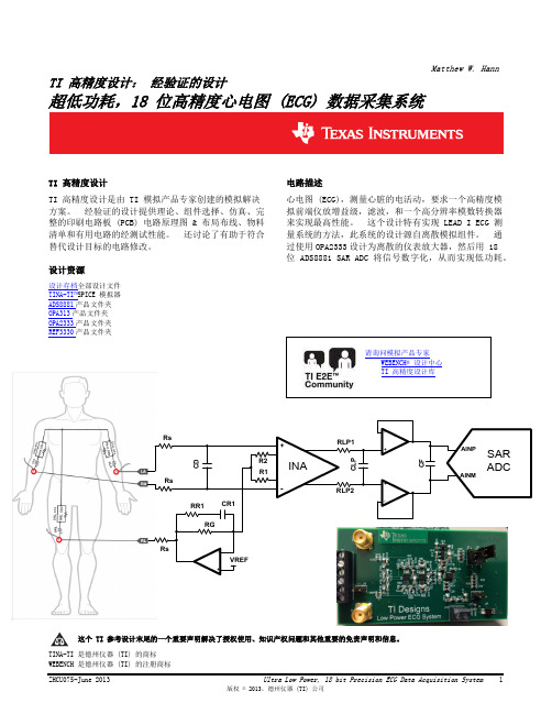
图 2: 完整的离散低功耗 ECG DAQ
2.1 ECG 测量的背景
ECG 是将离子极化 / 去极化从心脏肌肉活动转换为一个可测量的电信号,可检测此电信号并可被用来确定 正常与有问题心脏波标志之间的关系。 为此,测量必须是精确且稳定耐用的。 虽然整个 ECG 字段包括 一个很多不同参考配置测量值的总和(也就是胸导联,威尔逊中心电极,导联 l,导联 ll,导联 lll), 这个设计只关注 LEAD I 测量,它是左臂 (LA) 和右臂 (RA) 之间形成的电势。 ECG 信号相对于右腿基准 导联的差分信号,通常在 100µVpp – 2mVpp 的范围内,并且包括高达 200Hz 的谐波;因此,小信号必须 被过滤、缓冲以及放大,这样,一个洁净的信号可被 ADC 数字化。
RG2 10k
RG1 10k
3 ++ 4-
2
U1A OPA333
1
RLP1 10k
43 ++
5
Riso1 1k
1
U2A OPA333
VDD
RF1 30k RF2 30k
2
4-
RLP2 10k
1
3 ++
5
U1B OPA333
VDD
CLP 50n
+
Vin Sample -
VDD
3 ++ 4-
5
U2B OPA333
Gain tage
3
+
Background-subtraction of fast-scan cyclic staircase voltammetry at
Biosensors &Bioelectronics 13(1998)1297–1305Background-subtraction of fast-scan cyclic staircase voltammetry atprotein-modified carbon-fiber electrodesMark A.Hayesa,*,Eric W.Kristensen b ,Werner G.KuhrcaDepartment of Chemistry and Biochemistry,Arizona State University,Tempe,AZ 85287-1604,USAbAbbott Labs,Chicago,USAcDepartment of Chemistry University of California,Riverside,USA Received 16February 1998;received in revised form 8June 1998;accepted 30June 1998AbstractBackground-subtraction techniques were applied to the voltammetry of nicotinamide adenine dinucleotide (NADH)at protein-modified carbon-fiber microelectrodes.The background currents at carbon-fiber electrodes were stable and voltammetric scans immediately before or after the analyte were effectively used for background subtraction.Digital step-potential waveforms were used to excite these carbon-fiber electrodes,where the resulting voltammetric analysis assessed the optimal switching and initial potentials and the electrochemical response time was determined.The initial potential was 0.0V and the switching potential 1.1V (versus Ag/AgCl)and the response time was approximately 300ms.Some sensitivity to NADH was lost and voltammetric prescans were required at protein-modified electrodes to obtain a stable baseline.Current versus time was assessed by the average current of the faradaic region from each voltammogram and by differential current;the average current minus the current from a non-faradaic potential range.Differential current assessments discriminated against artifacts caused by pH (as high as 1.0pH unit)and ionic strength flux (100mM).These background-subtraction techniques allowed the faradaic information to be obtained quickly and conveniently while maximizing sensitivity and maintaining selectivity.©1998Elsevier Science S.A.All rights reserved.Keywords:Avidin–biotin;Background-subtracted voltammetry;Carbon-fiber electrode;Fast-scan cyclic voltammetry;NADH voltammetry;Protein modified microelectrodes1.IntroductionFast-scan cyclic staircase voltammetry (FSCSV)at microelectrodes has become a well established tech-nique.This technique has led to an exceptional degree of spatial (Յ5m)and temporal (Յ20ms)resolution,especially for monitoring stimulated release of easily oxidized neurotransmitters and metabolites in vivo (O’Neil,1974;Wightman et al.,1988).One compli-cation of a fast scan rate is the concomitant increase in the background capacitive current (Bard and Faulkner,1980).However,this background current at carbon elec-trode surfaces is remarkably stable.The stability of this current from scan to scan (given a consistent local buffer environment)offers a convenient and simple source of background scans for subtraction schemes.This scheme*Corresponding author.Tel:ϩ16029652566;Fax:ϩ16029652747;E-mail:mhayes@0956-5663/98/$-see front matter ©1998Elsevier Science S.A.All rights reserved.PII:S 0956-5663(98)00093-1leads to the improvement of detection limits (Wiedemann et al.,1991;Kawagoe et al.,1993b).In this paper,this method is applied to nicotinamide adenine dinucleotide (NADH)voltammetry associated with enzyme-modified carbon-fiber electrodes.This class of modified electrodes provides a method to monitor non-electroactive species in physiologically relevant time-scales and volumes (Kuhr et al.,1993).The enzymes that use NADH as a co-factor include some 200species and each may be coupled to this class of biosensors via an avidin–biotin linkage system (Kuhr et al.,1993).NADH/NAD +-linked electrochemical probes offer new types of enzyme-based biosensor for a large number of analytes,but the fundamental operating parameters must be investigated.Background-subtraction can digitally minimize or remove the background current.For a FSCSV experi-ment,the processed data is described as a background-subtracted cyclic voltammogram (BSCV)in which a full cyclic voltammogram is generated each 200ms1298M.A.Hayes et al./Biosensors&Bioelectronics13(1998)1297–1305(Wightman and Wipf,1990;Kuhr et al.,1993).For this background-subtraction procedure,the analytical per-formance of the FSCSV measurement is enhanced in numerous ways,most notably by addressing the trade-off between temporal resolution and current signal-to-noise ratio(while retaining qualitative information). Digital background-subtraction techniques permit sensi-tive measurements over a short time course without decreasing the scan rate to diminish background capaci-tive currents.Separation of the faradaic information of the analyte from the background ensures that the inherent selectivity of the FSCSV measurement is also retained.This selectivity is quantitated by the position of the oxidative and/or reductive peak potential which differentiates the species on the basis of their electron transfer kinetics.This technique allows this qualitative information to be recorded in a fast,sensitive manner (Wightman and Wipf,1990).Fast-responding,enzyme-modified carbon-fiber microelectrodes,which transduce the non-electroactive analytes into an electroactive species through the interac-tion of cofactors have been developed(Pantano and Kuhr,1993).This microelectrode utilizes avidin–biotin interaction to immobilize enzymes onto the electrode surface.The dehydrogenase family of enzymes is parti-cularly attractive for this purpose since their activity is linked to the electroactive cofactor,NADH.The cofactor generated in this manner acts as an electron-transfer mediator that can be monitored by FSCSV at carbon-fiber surfaces.While the FSCSV for the oxidation of NADH produces high faradaic currents and low overpot-ential at bare carbon-fiber microelectrodes,the response at an enzyme-modified surface is diminished(Pantano and Kuhr,1993;Hayes and Kuhr,1998a).The dimin-ished FSCSV response occurs because the carbon-fiber surface is both the site of electron transfer and of enzyme-immobilization.A quantitative balance between these two tasks has been attempted and,because these are competing activities,some voltammetric perform-ance has necessarily been sacrificed(Pantano and Kuhr, 1993;Hayes and Kuhr,1998a,b).Factors were evaluated that control the quality of a BSCV generated at a dehydrogenase-modified carbon-fiber microelectrodes to allow full interpretation of the available information.Near the detection limit for NADH the results of these background-subtraction para-meters were most pronounced.A digitally generated potential-step waveform was used to excite carbon-fiber electrodes to generate a BSCV.The carbon-fiber electrodes required an electro-chemical pretreatment to provide low overpotential and high faradaic currents for the oxidation of NADH.These pretreated electrodes were used to characterize the back-ground-subtraction technique.First,the switching and initial potentials were determined and the response time was then characterized.Background currents were found to drift more at protein-modified electrodes than freshly polished electrodes,but stable background currents were obtained after a series of voltammetric prescans were performed.To obtain qualitative voltammetric infor-mation,the scans used for background subtraction must be chosen,both in number and position.These choices were characterized for sensitivity and stability.Improve-ment of the signal-to-noise ratio was obtained by both full-scan summing and averaging,and averaging each three adjoining data points within a single scan.Current artifacts caused by pHflux and ionic strength changes were eliminated by using information available within each scan.Current arising in non-faradaic potential regions was used to compensate those within faradaic, or information-containing,regions.These data manipu-lations reduced sensitivity,but could compensate for pH flux up to1.0pH units and ionic strength changes of 100mM.These digital excitation and data manipulation techniques provide a convenient and powerful method to obtain information quickly and with high sensitivity for the electrochemical measurement of NADH.2.Experimental2.1.ChemicalsGlutamate dehydrogenase(GDH,40units/mg,E.C.1.4.1.3),NADH,ExtrAvidin,and1-ethyl-3-((dimethylamino)propyl)carbodiimide(EDC)(Sigma Chemical Co.,St Louis,MO,USA);sulfo-NHS-LC-biotin(Pierce Chemical Co.,Rockford,IL,USA),and poly(oxyalkylene)diamine(Jeffamine™ED-2001;Tex-aco Chemical Co.,Houston,TX,USA)were used as they were received.Phosphate buffer(PBS;0.15M NaCl,0.10M Na2HPO4,pH8.5)was prepared with reagent grade chemicals in water purified by a Milli-Q water purification system(Millipore,Bedford,MA, USA).All FSCSV measurements were conducted in pH 8.5phosphate buffer.2.2.Carbon-fiber microelectrodesThe fabrication of carbon-fiber microelectrodes has been described previously(Pantano and Kuhr,1993).All 10m diameter carbon-fiber microelectrodes(Thornel P-55S;Amoco Performance Products,Greenville,SC, USA)were bevelled at a30°angle for10min on a pol-ishing wheel covered with1m diamond paste(Metadi II;Buehler,Lake Bluff,IL,USA).Residual polishing materials were removed by sonicating the electrodes in hot toluene and then in de-ionized water for10s.Unless otherwise noted,all10m diameter carbon-fiber microelectrodes were electrochemically treated in1.0M HCl by a3s,50Hz cyclic potential waveform generated betweenϪ0.2V and1.8V(versus Ag/AgCl).All321299 M.A.Hayes et al./Biosensors&Bioelectronics13(1998)1297–1305m diameter carbonfiber(Textron Specialty Materials, Lowell,MA,USA)microelectrode surfaces were pol-ished on a glass wheel embedded with8–10m dia-mond particles(Sutter Glass,Novato,CA,USA).These 32m diameter carbon-fiber electrodes were further activated with aϪ0.2to2.0V(versus Ag/AgCl),50 Hz waveform in pH8.5PBS(Hayes and Kuhr,1998a). The derivatization of carbon-fiber microelectrodes with biotinylated-GDH has been described in detail (Pantano and Kuhr,1993).In brief,the modified egg-white protein,ExtrAvidin,serves to link biotinylated-(sulfo-NHS-LC-biotin)GDH to a biotinylated-(sulfo-NHS-LC-biotin)hydrophilic tether(Jeffamine ED-2001) which is covalently bound(EDC linkage)to the carbon-fiber surface.2.3.InstrumentationFast-scan cyclic-staircase voltammetry was performed with an EI-400potentiostat(Cypress Systems,Lawr-ence,KS,USA)which was designed to accommodate placement of the working electrode pre-amplifier inside a faraday cage.All staircase cyclic voltammetric wav-eforms were generated,and currents acquired,with an 80486PC microcomputer utilizing a12-bit,20kHz A/D–D/A interface(Labmaster DMA;Scientific Sol-utions,Solon,OH,USA).All potentials reported were referenced to a0.4mm o.d.Ag/AgCl electrode.A400 kHz digital oscilloscope(Nicolet instruments Model 310;Madison,WI,USA)was used to acquire the stair-case waveform shown in Fig.1(a);the waveform was acquired with1ms(Fig.1(a)inset)and200ms(Fig. 1(a))oscilloscope time constants.All currents were recorded with a faraday cage with aflow-injection analy-sis(FIA)system previously described,where buffer(1.5 ml/min)was now controlled by a peristaltic pump (Model203;Scientific Industries,Bohemia,NY,USA) (Kuhr et al.,1993).All FSCSV measurements acquired werefiltered within a1–3kHz range by the two-pole, low passfilter(3db between1.5Hz and15kHz)of the EI-400potentiostat.2.4.Data manipulation and presentationFIA data may be presented in a variety of formats. Qualitative data for BSCV in cyclic voltammetric-format (CV)was obtained by subtracting background scans from analyte scans.The background scans may be chosen from data sets before or after the analyte plug. Time versus current information is presented in two distinct formats:average current and differential current. The average current versus time plots is the average cur-rent of a potential range from each cyclic voltammog-ram-format data set(typically including the peak poten-tial(E p)of the analyte).This potential range for averaged current may be varied and was investigated.Differential current plots subtracted the average current from a potential range where faradaic analyte current is absent from the average current data.This data manipulation allows changes in buffer composition which influence electrode capacitive currents to be compensated.The current changes caused by capacitive influence will be reflected equally in faradaic and non-faradaic regions. Therefore,this non-faradaic current region provides a background-subtraction source for compensation of these artifact currents.Plots may also be created in a three-dimensional view.Some data was exported as an ASCIIfile and manipulated in Lotus1-2-3(Lotus Devel-opment Corp.,Cambridge,MA,USA)or Excel (Microsoft,Redmond,WA,USA).3.Results and discussionThe exceptional spatial and temporal resolution of a fast-scan voltammetric measurement is made possible by the rapid electrochemical response of microelectrodes (approximately a1s time constant)(Wightman and Wipf,1990).An experiment may be performed at a scan rate of100V/s,when the oxidative and reductive scans across a1V region are completed in20ms.When these scans are repeated at100Hz,the time course of the measurement provides sub-second temporal resolution (approximately200ms),where selective and sensitive data can be recorded in the same measurement (Wightman et al.,1988).Digitally generated step-potential waveforms are instrumental for these measurements(Bilewicz et al., 1989;Murphy et al.,1989;Karpinski and Osteryoung, 1993).With fast linear scan rates,the capacitive (residual)current(i c)increases linearly with an increas-ing scan rate,whereas the faradaic current(i f)follows only a square root dependence.At high scan rates,the capacitive current is dominant.The use of step-potential waveforms and time-delay digital data acquisition min-imize the contributions of capacitive currents at fast scan rates,thus allowing the relative amount of faradaic cur-rent to increase.A cyclic staircase potential waveform(Fig.1(a))is described by its potential step-height and its potential step-width,in which the scan rate(V/s)is determined by their ratio(Howell et al.,1986).The advantage of this technique arises from the temporal control of the current measurement.Digital sampling provides for acquisition of the current at any point along the potential step width.Since the decay of capacitive currents are fast(e−t/Rc,where t is time,R is the electrode resistance and C is the electrode capacitance),and the decay of the faradaic current follows a slower time dependence(t1/2), the current is recorded at the end of the potential step (arrows,Fig.1(a)inset).The background current at a carbon-fiber microelec-1300M.A.Hayes et al./Biosensors&Bioelectronics13(1998)1297–1305Fig.1.Fast-scan cyclic staircase voltammetry(100V/s,100prescans)at a polished and electrochemically pretreated,10m diameter carbon-fiber microelectrode.(a)Cyclic staircase potential waveforms,in which the oxidative and reductive scans across a1.2V region(tϭ22ms)were repeated every200ms.(a,Inset)An individual potential step was18.30mV high and0.18ms long.All currents were sampled at the end of each potential step(arrows).(b)Three-dimensional view of the oxidative portion,plotted in an upward direction,of the FSCSV experiment.(c)Average oxidative current versus time when the time course for the appearance of NADH is ascertained by monitoring the oxidative current between714 and934mV versus Ag/AgCl.(d)Cyclic staircase voltammograms(average of10scans)acquired during(boxes)and after(triangles)the4s FIA injection of100M NADH.(e)BSCV created by the digital subtraction of the two voltammograms from(c).1301 M.A.Hayes et al./Biosensors&Bioelectronics13(1998)1297–1305trode contains not only capacitive components but also faradaic components.The faradaic component of the residual background current stems from the carbon-oxy-gen moieties that are localized on the carbon surface, most notably quinones and hydroquinones(Wiedemann et al.,1991;Kawagoe et al.,1993a).While the use of digital staircase waveforms discriminates against capaci-tive currents,the background current is significantly affected by these surface-bound faradaic processes (Howell et al.,1986;Kawagoe et al.,1993b).Since the background current is only partially discriminated against with this technique,further improvements are needed.Far greater results for improving i f/i c and the signal-to-noise ratios have been reported with background-current subtraction(Howell et al.,1986).For this technique,FIA provides the stable background-currents because the environment of the microelectrode surface is constant, except for the introduction of the sample bolus (Engstrom et al.,1988).This stable background current is necessary to prevent distortion of the faradaic infor-mation(Howell et al.,1986;Kawagoe et al.,1993a,b).A well-formed electrochemical response to a100M bolus of NADH and a stable background current is shown in Fig.1(b and c)at a polished carbon-fiber microelectrode.This demonstrates a consistent back-ground current,and the introduction of analyte does not produce artifacts(odd peak shape,hysteresis,etc.).To optimize FSCV further for the electrochemical measurement of NADH when performed at carbon-fiber microelectrodes,several electrochemical pre-treatments were explored.These were examined for their ability to optimize the quality and reproducibility of the NADH response for FSCV.A mild anodic treatment in HCl pro-duced low overpotential and high faradaic currents for oxidation of NADH(Pantano and Kuhr,1993)(Fig.1(d and e))at10m diameter carbon-fiber electrodes, whereas32m carbonfibers required treatment in pH 8.5PBS to produce similar results(Hayes and Kuhr, 1998a).While low overpotential and high faradaic cur-rents can be observed at freshly polished carbon-fiber surfaces,there was considerable variability from elec-trode to electrode.The BSCV shown in Fig.1(e)was generated at a pretreated electrode by subtracting vol-tammetric scans acquired after the FIA injection(Fig. 1(c),triangles)from the voltammetric scans acquired during the injection(Fig.1(c),boxes).This result dem-onstrates a BSCV where the facile electron-transfer information is retained through the subtraction process. Measurement of the response time of this system was accomplished by monitoring the current from800to 1100mV(faradaic current from oxidation of NADH) versus time(Fig.1c).The response observed to this square-wave input was an electrochemical measurement characteristic of the temporal response of the sensing system.The response of a pretreated carbon-fiber microelectrode to the injection of NADH in a FIA-FSCSV experiment is quite rapid(Fig.1(c));the time required to reach63%of the steady-state current is approximately300ms.3.1.Selection of initial and switching potentials While FSCSV of the NADH at a polished,electro-chemically pretreated carbon-fiber microelectrode typi-cally exhibits an oxidative peak potential at800mV ver-sus Ag/AgCl(Fig.1(e)),this anodic wave is shifted more than300mV positive following the enzyme-modifi-cation procedure(Pantano and Kuhr,1993;Hayes and Kuhr,1998b).A switching potential of1100mV(versus Ag/AgCl)was used because it was the maximum poten-tial allowed without significant interference from the oxidation of the background buffer.The possibility of using the reductive NADH current to improve sensitivity is eliminated since oxidation of NADH at carbon elec-trodes is chemically irreversible(Moiroux and Elving, 1979,1980).The choice of an initial potential is influenced by other factors that are associated with the use of these probes in vivo.In previous in vivo FSCSV determinations for stimulated release of catecholamines,aϪ400mV (versus Ag/AgCl)initial potential was required (Wightman et al.,1988).This value was chosen to ensure the complete reduction of the oxidized quinone present on numerous biological molecules of interest generated during the oxidative voltammetric scan.Fluc-tuations in the concentrations of these species could interfere with the analysis of NADH.Nonetheless,even if no detectable quinone/hydroquinone redox couple were present in solution,quinone and hydroquinones on the carbon-fiber surface itself would always be present (Kawagoe et al.,1993a).An initial potential of0.0V (versus Ag/AgCl)was chosen to eliminate the quinone/hydroquinone redox couple,thus avoiding poss-ible artifacts from this process altogether.3.2.Background current driftRepetitive cycling of a potential waveform will improve the stability of the background current,when this cycling allows the electrode surface to approach a steady state(Kinoshita,1988).In vivo voltammetry experiments typically require a10min cycling of the potential waveform after implantation before any data is acquired(Wightman et al.,1988).The majority of this voltammetric degradation occurs within thefirst few minutes after implantation.With carbon-fiber surfaces, the sensitivity is diminished,but the background currents will remain stable for the remainder of the experiment and therefore background-subtraction techniques may be employed.A carbon-fiber surface with immobilized enzymes1302M.A.Hayes et al./Biosensors &Bioelectronics 13(1998)1297–1305also requires cycling of the voltammetric waveform to use the background-subtraction technique.Quantitative evaluation of the background current upon repetitive cycling of the voltammetric waveform was investigated (Fig.2).The number of conditioning prescans to elimin-ate or minimize the drift observed at an enzyme-modi-fied electrode surface was determined.A flat baseline was produced with approximately 700prescans,and 1000prescans were used before analytical voltammog-rams were recorded (Fig.2(b)).This number of prescans can be generated in 2–3min in a FSCSV experiment depending on the exactconditions.Fig.2.Baseline drift as a function of the number of prescans.(a)The oxidative current of 100M NADH (4s FIA injection),between 800and 1100mV (forward scan),versus time.The two time courses were at the same 32m diameter carbon-fiber microelectrode follow-ing 100prescans (top)and 700prescans (bottom).(b)Baseline slope versus the number of prescans.The baseline-slope data was acquired at a 32m diameter carbon-fiber microelectrode from the respective oxidative current versus time plots.3.3.Selection of voltammograms for BSCVThe sensitivity of FSCSV for NADH was degraded by the fabrication procedure for enzyme-modified elec-trodes.The initial faradaic response for the NADH oxi-dation was diminished by more than 84%,and the oxi-dative peak potential shifted.This reduces the clarity with which the NADH oxidative signal can be inter-preted and requires that all measures be examined to maximize the signal-to-noise ratio.The reduction in sensitivity caused by these voltam-metric shifts led to a quantitative investigation of the selection of CVs used for the background subtraction.Consistent results were obtained whether the subtraction CVs were obtained immediately before or immediately after the analyte plug.At high concentrations,there is no significant difference between using the background scans from before or after the analyte plug.For this set of eight electrodes exposed to 100M NADH in a 4s plug,there was only one difference (Table 1),an increase of 8%(only 0.59nA)in i p .Due to this slight increase,background scans were used from after the ana-lyte plug.However at lower concentrations even small differences are important.Thus,the slight under-subtrac-tion observed when the background is taken before injec-tion of sample can severely affect the observed response.Therefore,it is generally best to use background obtained after the injection of sample,since this is more representative of the electrode condition during the sam-ple.A single electrode was used to investigate another aspect of the background scans used for subtraction.Background scans were taken from long before (0–2s,Fig.2(a))and long after (15–17s,Fig.2(a))the analyte bolus and subtracted.The resultant CVs had i p of 6.0nA;E p of 930and i p of 6.6nA;E p of 930,respectively.While the background currents generated at the carbon-fiber surface remained remarkably stable throughout the 17s (85scans)of the FIA measurement,it is notable that the electrode does continue to change with time.Therefore,it is best to minimize the time allowed between sample and background scans.The optimum subtraction is obtained by using the background immedi-ately following the removal of the sample.The number of scans to be used for both the analyte and the background data sets were also investigated.The number of scans for both the analyte data set and the background data set were kept equal and increased from 1to 16(Fig.3).The noise from the resultant BSCV was plotted versus number of scans averaged,when the noise was reduced by an approximate square root-dependence with the number averaged.However,no significant S/N enhancement was found after 10scans were averaged,indicating that unknown factors other than random noise contribute significantly to the noise for these electrodes.Noise reduction was also performed by averaging1303M.A.Hayes et al./Biosensors&Bioelectronics13(1998)1297–1305Table1Position of scans used for background subtraction for BSCVLocation of background scans relative to analyte bolus(6-4s)aElectrochemical parameter Before(1-3s)After(9-11s)Change Percentage changeE p(mV)856Ϯ17862Ϯ16--i p(nA)b 6.50Ϯ0.427.09Ϯ0.66ϩ0.59Ϯ0.30ϩ8Ϯ4.6a All errors quoted are SEM.b Average current from800to1100mV minus average current from200to400mV versus time for a4s FIA injection of100MNADH.Fig.3.Noise of background-subtracted cyclic voltammogram versus number of scans averaged.Both the background and signal scan num-bers were increased equally.Data taken from FIA experiment similar to that shown in Fig.1(c).each three points of adjoining data on the background-subtracted CVs.For the average of three subtracted CVs, the noise was0.82nA and nine three-point averages of a single CV resulted in0.66nA of noise.A combination of a high number of averaged CVs and three-point aver-aging(11scans,nine three-point averages)reduced noise further,but only to0.60nA.The number of scans util-ized throughout the rest of this work was set at10to ensure noise spikes(even smoothed with the three-point averages)did not give false E p or i p values.3.4.Differential current versus time measurements Electrochemical detection is not immune to its local environment:surface changes in pH,ionic strength,etc., especially near detection limits may cause artifacts (Wiedemann et al.,1991;Kawagoe et al.,1993a).Back-ground capacitance currents caused by these processes were minimized by an additional quantitative data manipulation.Current obtained in a voltage range where no relevant faradaic current occurred was subtracted from the oxidative faradaic current.Capacitive effects are independent of the value of the potential,depending only on the scan rate.So,the capacitive currents in the voltammogram which overlap the faradaic signal are equal to those in the non-faradaic region.Signal optimization for time course measurementswas examinedfirst.The signal potential range(R sig)was varied and the signal intensity recorded(Fig.4(a)).Forthis particular electrode(E pϭ860mV,Fig.4(a)),the maximum signal intensity occurs when the voltage rangeencompasses E p and greater,while minimizing otherpotential ranges.Current was collected fromෂ50mV less than E p to1100mV for the differential current ver-sus time plots.Signal optimization for differential time course measurements examined the background potential range (R bkgrd)for the subtractive current.ThebackgroundFig.4.Potential range optimization for differential current versus time data.(a)Potential range versus current intensity for average cur-rent plots.E p for NADH at this carbon-fiber electrode was860mV. Range used was from the data point value to1.1V.(b)Potential range used for subtraction current versus current intensity for differential cur-rent plots.Average current values were obtained from800to1100mV.。
OB2362L Datasheet_Acbel_150305
O
n-
Br ig
©On-Bright Electronics
ht
co
nf id
Valley
Confidential -4-
en
Ac be
Diode short
LEB
AVDD
Preliminary Datasheet OB_DOC_DS_2362L00
l
CS FB
OB2362L
Adaptive Multi-Mode PWM Controller
Ac be
-40 to 150 ℃ -40 to 85 ℃ -55 to 150 ℃ Preliminary Datasheet OB_DOC_DS_2362L00
l
OB2362L
Adaptive Multi-Mode PWM Controller
TERMINAL ASSIGNMENTS
Pin Name GND FB DEM CS VCC Gate I/O P I I I P O Description Ground Feedback input pin. The PWM duty cycle is determined by voltage level into this pin and the current-sense signal at Pin CS.
FEATURES
■ ■
■ ■ ■ ■
APPLICATIONS
O
n-
Br ig
©On-Bright Electronics
ht
TYPICAL APPflyback converter for ■ General power supply ■ Power Adapter
斜坡补偿2
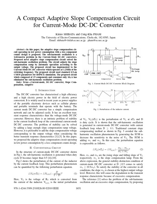
A Compact Adaptive Slope Compensation Circuitfor Current-Mode DC-DC ConverterKimio SHIBATA and Cong-Kha PHAMThe University of Electro-Communications,Chofu-shi,182-8585,JapanEmail:shibata@vlsilab.ee.uec.ac.jp;pham@ee.uec.ac.jpAbstract—In this paper,the adaptive slope compensation cir-cuit operating in low power consumption with a less componentcounts design is proposed.The sub-harmonic oscillation is awell-known problem in the Current-Mode DC-DC converters.Proposed novel adaptive slope compensation circuit solved thesub-harmonic oscillation problem.The circuit adjusts the slopecompensation ramp by automatic operation according to theoutput voltage.The proposed circuit has implemented to theCurrent-Mode DC-DC converter which operates at1.2MHz of theswitching frequency.The proposed circuit used standard0.5μmCMOS parameters for HSPICE simulation.The proposed circuitwhich composed of15components and consumes only10μA haseliminated the sub-harmonic oscillation problem.Index Terms—Current-mode,DC-DC converter,Slope Com-pensation,AdaptiveI.I NTRODUCTIONThe DC-DC converter has characterized a high efficiencyand a high electric power in thefield of electric powerconversion.It is widely used in recent years as power suppliesof the portable electronic devices such as cellular phonesand portable terminals that operate with the battery.Thecurrent mode DC-DC converter has a simple compensationnetwork and can be adjusted easily.It has an excellent tran-sient response characteristics than the voltage-mode DC-DCconverter.However,there is an intrinsic problem of stabilityin the current feedback loop of the conventional current-modeDC-DC converter.The problem of stability can be solvedby adding a large enough slope compensation ramp voltage.However,it is preferable to add the slope compensation voltagecorresponding to the output voltage when considering thebetter transient response characteristics[1]-[3].In this paper,we proposed the adaptive slope compensation circuit operatingin low power consumption by a less component counts design.II.C ONVENTIONAL C IRCUITIn the structure of current-mode DC-DC converter shownin Fig.1,the sub-harmonic oscillation is generated when dutycycle D becomes larger than0.5[4]-[10].Fig.2shows the perturbation of the current of the inductorby the current feedback loop.This perturbation phenomenoncan be quantified by the following perturbation equation.V L(nT S)= V L(0)(−D1−D)2(1)Here,V L is the voltage of R S which is converted from the current of the inductor.V L(0)is the initialperturbationFig.1.Current-Mode DC-DC Converter BlockDiagram.Fig.2.Perturbation of the inductor current.of V L,V L(nT S)is the perturbation of V L at nT S and D is duty cycle.It is shown that the sub-harmonic oscillation is generated in current-mode DC-DC converter with current feedback loop when D≥0.5.Traditional constant slope compensating method as shown in Fig.3avoided the sub-harmonic oscillation phenomenon by generating the SUM to decrease the sensitivity to the noise of V L.The SUM is adding m1and m a.In this case,the perturbation equation is expressible as follows.V L(nT S)= V L(0)(−m2−m am1+m a)2(2) Here,m1and m2are the rising slope and falling slope of V L respectively.m a is the slope compensation lamp.From the above expression,the general stability distinction condition of current-mode DC-DC converter at D≥0.5comes to satisfy m a≥(0.5m2).To satisfy the stability of the converter in all conditions,the slope m2is chosen at the highest output voltage level.However,this will cause the degradation in the transient response characteristic because of excessive compensation. The reference[1]solves the problem of the sub-harmonic oscillation and an excessive slope compensation,by proposingFig.3.Traditional constant slope compensating method.Fig.4.Previous adjustable-slope compensating circuit[1].a circuit which automatically adjusts the slope voltage.In the Fig.4,the slope m s of voltage SUM is defined as follows.m s=m1+m2=V IN−V OUTL(ind)+V OUTL(ind)=V INL(ind)(3)Here,L(ind)is inductance of the inductor.The three switchesexecute the following operation in every switching cycle forthe inductor.State A:switch A is on,then the Power MOSswitch become on and the current begins toflow to the induc-tor State B:switch B is on,then the constant current source Istarts charging the capacitor C S.The voltage slope is decidedby the ratio of input voltage V IN and inductance L(ind).That isV IN/L(ind).Current source I is proportional to input voltage V IN while C S is defined by the relation V IN/L(ind)=I/C S. State C:When the inclination of V IN/L(ind)reaches the error amplifier output V C,the SUM is reset by switch Cto the ground level.The current source I of this circuitgenerates the slope compensation ramp in proportion to inputpower supplyV IN.Hence,the noise voltage of superimposedinput power supply will be also superimposed to the slopecompensation ramp.As a result,there is a possibility that thenoise immunity from the input power supply is decreased. The reference[2]proposed an adaptive slope compensation circuit.In the Fig.5,the slope of the compensated currentisFig.5.Previous adjustable-slope compensating circuit[2].defined as follows.I SLOPE=V CAP(V OUT−0.5V IN)V REF R0(4) The circuit of the reference[2]is composed of two operational amplifiers,a comparator and other components.The reference[3]improved the bandwidth of the DC-DC converter using a quadratic slope compensation.The slope compensation ramp is generated by sensing the input voltage of the V IN.The novel compensation circuit has achieved more than60degree phase margin in the total feedback loop. However,since the slope compensation ramp voltage is a function of the V IN,the noise immunity of the V IN may cause the instability problem.III.P ROPOSED A DAPTIVE S LOPE C OMPENSATIONC IRCUITThe proposed circuit is a output voltage adaptive slope com-pensation ramp voltage generator.The circuit automatically generates the slope compensation ramp voltage for any output voltages.A.Circuit StructureThe proposed circuit satisfies m a=V OUT/L(ind).The slope compensation ramp voltage is automatically adjusted accord-ing to output voltage V OUT and the standard of stability distinction is m a≥(V OUT/2L(ind)).Fig.6shows the proposed circuit.For MOS transistor operating in saturation region,the following relations are given [10].I d=μn C OX2WL(V GS−V TH)2(5) V GS=I dμn C OX2WL+V TH(6)In this case,the gate-source voltage V GS between MOS transistors to whichI d(W/L)is equal,is the same.Here,W and L are the channel width and channel length of MOS transistor. As a result,the variation of V TH by the manufacturing process and the operating temperature is counterbalanced.This effect is the same to the differential stage of the amplifier.Theproposed circuit applied this feature.V g is a bias voltage for P3andP4.Fig.6.Proposed adaptive slope compensation circuit.For the simplification,let’s assume (W/L)P1=(W/L)P2,(W/L)P3=(W/L)P4,(W/L)P5=(W/L)P6.The transconduc-tance of N1and M1is expressed with g m .When the condition of 1/g m R,1/g m R 1is satisfied,the following relation is obtained.I R1=(V OUT +V GSP −V GSN )/R 1I R =(V GSP −V GSN )/R I dP6=I R1−I RHere,I R1and I R are the current that flow to R1and R.I dP6is the drain current of P6.V GSP ,V GSN are the gate-source voltage of PMOS transistor and NMOS transistor,respectively.When R=R1=r ,(W/L )M2=(W/L )M3is satisfied,the following relations are obtained.I dP6=I R1−I R =V OUT /r I dM3=V OUT /rThus,the slope compensation ramp can be expressed as follows.m a =(I dM3)(t )C =(m )(V OUT )(t )(C )(r )(7)Here,t is the turn-off time of M4.m a can be utilized as anadaptive slope compensation since it is positively proportional to V OUT .yout and Simulation ResultsFig.7shows a block diagram of a DC-DC converter which is used the proposed adaptive slope compensation circuit (ADPSLP).Fig.8shows the chip layout using 0.5μm standard CMOS design rules.The adaptive slope compensation circuit (ADPSLP)has been put on underneath of the NMOS transis-tor.In order to limit input voltage range of ADPSLP,V OUT has divided by R3and R4.The value of m a at V OUT =2V and L (ind)=4.7μH ism a =V OUT /L (ind)=0.43A /μs.Fig.7.Block diagram with proposed adaptive slope compensationcircuit.Fig.8.Chip LayoutHere,the DC-DC converter has current-voltage gain of 1for inductor current-sensing.Thus,the voltage slope m aV con-verted from current slope ma is rewritable to m aV =0.43V /μs.The simulation condition are C=5pF,and t =1μs.Thus,I dM3=C (V OUT )/t =2.15μA.I dM3is charged to the capacitor C.Fig.9,10and 11shows the simulation result of the proposed circuit for the DC-DC Converter.The simulation has performed at V IN =2.8V ,V OUT =2V ,I OUT =0.4A,L =4.7μH ,D =0.7,CLK =1.2MHz.Where,the CLK is a switching frequency of the DC-DC Converter.I L is the inductor current.”Current Sense”is the sense current of the inductor.”m a ”is the slope compensation ramps.Fig.9shows the inductor current I L without the slope compensation (m a =0).The sub-harmonic oscillation is observed.Fig.10shows the result of m a =(0.1)m 2.The sub-harmonic oscillation is observed.Fig.11shows the result of m a =m 2.The sub-harmonic oscillation is not observed.Fig.12shows the result of m a when the V OUT is changed from 0V to 3V .The ramp voltage of m a increases accurately in proportion to V OUT .The proposed circuit has 15components in total which includes V g and the charge circuit.The current consumptionof the proposed circuit is only10μA.Hence,the proposed adaptive slope compensation circuit has a feature of the compact circuit and the low power consumption.Fig.9.Simulation result of IL at m a=0Fig.10.Simulation result of IL at m a=(0.1)m 2Fig.11.Simulation result of IL at m a=m2IV.C ONCLUSIONThe supply voltage of electronic equipments is diversified. The power supply voltage for the portable electronics ap-plication is in the range from0.8V to3.3V.Generally,theFig.12.Simulation result of m2vs V OUToutput voltage is programmed according to the external resistor of integrated circuit.As a result of the HSPICE simulation, no sub-harmonic oscillation at a duty ratio of D≥0.5 was observed on the proposed adaptive slope compensation circuit.Moreover,the proposed circuit has a compact circuit configuration and a feature of low power consumption.The circuit composed of15components and consumes10μA. Since it is necessary to program the slope compensation ramp tofit any output voltage for the Current-Mode DC-DC Converters,the proposed novel low power and compact adaptive slope compensation circuit has a good opportunity to solve the sub-harmonic oscillation problem.R EFERENCES[1]Cheng-Chung Yang,Chen-Yu Wang and Tai-Haur Kuo,”Current-ModeConverters with Adjustable-Slope Compensating Ramp,”IEEE Asia Pa-cific Conference on Circuits and Systems2006,APCCAS2006,pp.654-657,Dec.2006.[2]Li Yanming,Lai Xinquan,Chen Fuji,Yuan Bing and Jia Xinzhang,”AnAdaptive Slope Compensation Circuit for Buck DC-DC Converter”The International Conference on ASIC2007,ASICON’07,pp.608-611,Oct.2007.[3]Yasuhiro Sugimoto,”A MOS current-mode buck DC-DC Converter witha240-kHz loop bandwidth and unaltered frequency characteristics usinga quadratic and input-voltage-dependent compensation slope”ESSCIRC,2009.ESSCIRC’09,Proceeding of14-18Sep.2009pp.460-463. [4]Zoltan Zansky,”Current Mode Converter With Controlled Slope Compen-sation,”United States Patent,Patent Number:4,837,495,Date of Patent: June.6,1989,[5]Raymond B.Ridley,”A New,Continuous-Time Model For Current-ModeControl,”IEEE Transaction on Power Electronics,V ol.6,NO.2,April 1991[6]Richard Tymerski,Duwang Li,”State-Space Model for Current Pro-grammed Pulsewidth-Modulated Converters”IEEE Transactions on Power Electronics,V ol.8,NO.3,July1993[7]Vatch´e V orp´e rian,”Fast analytical techniques for electrical and electroniccircuits,”Cambridge University Press2004,ISBN0-521-62442-8,pp.440-459[8]Robert W.Erickson,Dragan Maksimovi´c,”Fundamentals of Power Elec-tronics,Second Edition,”Springer Science,2001,ISBN978-0-7923-7270-7,pp.439-449[9]Abraham I.Pressman,Keith Billings,Taylor Morey,”Switching PowerSupply Design,Third Edition,”McGraw-Hill,2009,ISBN978-0-07-148272-1,pp.176-181[10]R.Jacob Baker,”CMOS Circuit Design,Layout,and Simulation,Revised Second Edition”IEEE Press-Wiley Interscience,2008,ISBN 978-0-470-22941-5,pp.143-145。
芯片AD654详细资料

0
500
0.06
0.1
0.20
0.4
–10
+10
0.20
0.40
0.05
0.10
50
kHz
% %
%
%/V %/V ppm/°C
ANALOG INPUT AMPLIFIER (Voltage-to-Current Converter) Voltage Input Range Single Supply Dual Supply Input Bias Current (Either Input) Input Offset Current Input Resistance (Noninverting) Input Offset Voltage vs. Supply VS = +4.75 V to +5.25 V VS = +5.25 V to +16.5 V vs. Temp (0°C to +70°C)
4.5
4.5 ±5
1.5 2.0
TEMPERATURE RANGE
Operating Range
–40
mA
mA
100
nA
500
nA
(+VS – 4)
V
µs µs
16.5ห้องสมุดไป่ตู้
V
36
V
± 18
V
2.5
mA
3.0
mA
+85
°C
NOTES 1At fMAX = 250 kHz; RT = 1 kΩ, CT = 390 pF, IIN = 0 mA–1 mA. 1At fMAX = 500 kHz; RT = 1 kΩ, CT = 200 pF, IIN = 0 mA–1 mA. 2The sink current is the amount of current that can flow into Pin 1 of the AD654 while maintaining a maximum voltage of 0.4 V between Pin 1 and Logic Common.
混合式自适应Kalman滤波算法
O 引 言
针对 Ka n滤波 发散 的不 同原 因 ,抑 制 自适应 Ka l ma l
ma n滤波 发 散 的 方 法 ,最 常 见 的 方 法 有 :S g- a 自适 应 aeHu 滤 波 法 [ ] 跟 踪 Kam n 波 法 _3、平 方 根 法 、贝 叶 斯 1 、强 ~ la 滤 2_ _
Ke r s k l n f t r h p " y a i p st n n ;t e is a ay i ;d t p i z t n a g r h ;Kam a i e y wo d : ama i e ;s i s d n m c o ii i g i s re n l ss a a o tmia i l o i m l o me o t l n fl r t
0 5 0 lo o
ts /
10 5
2) ( 0
( SP b D 风速发散的情况 )
由于 F () 惫 、G ( ) 为 已 知 ,△ ( ) 未 知 , 由 文 献 足 F 忌
[]可知 ,式 ( )可改写如下 2 5
c( c k+ 1 )一 F( ,( )4 G( ) ( )4 ( ) ) 志 - 尼 U 忌 - 尼 z
Bln l o ih b s d o d p i e k l n fle i g e d a g rt m a e n a a tv ama i rn t
W ANG n r o Qi-u ,XI ONG in bn,YE a — u,DENG i— ig,YANG Ja - i B oy Ju yn Na
wih r a—i a a c l c e yt e Gi n sa e me e .Th x e i e tr s lsi dc t h t h r p s d a a t ef t rp r t e l me d t o l t d b h l wi d n mo t r t e l ee p r n e u t ia e t a ep o o e d p i i e e — m n t v l
ADF4153资料
Fractional-N Frequency SynthesizerADF4153Rev. AInformation furnished by Analog Devices is believed to be accurate and reliable. However, no responsibility is assumed by Analog Devices for its use, nor for any infringements of patents or other rights of third parties that may result from its use. Specifications subject to change without notice. No license is granted by implication or otherwise under any patent or patent rights of Analog Devices. Trademarks and registered trademarks are the property of their respective owners.One Technology Way, P.O. Box 9106, Norwood, MA 02062-9106, U.S.A. Tel: 781.329.4700 Fax: 781.326.8703© 2004 Analog Devices, Inc. All rights reserved.FEATURESRF bandwidth 500 MHz to 4 GHz 2.7 V to 3.3 V power supplySeparate V P allows extended tuning voltage Programmable dual-modulus prescaler 4/5, 8/9 Programmable charge pump currents 3-wire serial interfaceAnalog and digital lock detect Power-down modePin compatible with theADF4110/ADF4111/ADF4112/ADF4113 and ADF4106 Programmable modulus on fractional-N synthesizer Trade-off noise versus spurious performanceAPPLICATIONSCATV equipmentBase stations for mobile radio (GSM, PCS, DCS, CDMA, WCDMA)Wireless handsets (GSM, PCS, DCS, CDMA, WCDMA) Wireless LANsCommunications test equipmentGENERAL DESCRIPTIONThe ADF4153 is a fractional-N frequency synthesizer that implements local oscillators in the upconversion anddownconversion sections of wireless receivers and transmitters. It consists of a low noise digital phase frequency detector(PFD), a precision charge pump, and a programmable reference divider. There is a Σ-Δ based fractional interpolator to allow programmable fractional-N division. The INT, FRAC, and MOD registers define an overall N divider (N = (INT + (FRAC/MOD))). In addition, the 4-bit reference counter (R counter) allows selectable REFIN frequencies at the PFD input. A complete phase-locked loop (PLL) can be implemented if the synthesizer is used with an external loop filter and a voltage controlled oscillator (VCO).Control of all on-chip registers is via a simple 3-wire interface. The device operate with a power supply ranging from 2.7 V to 3.3 V and can be powered down when not in use.FUNCTIONAL BLOCK DIAGRAMDATALECLOCK REF ININ A IN BMUXOUTFigure 1.ADF4153Rev. A | Page 2 of 24TABLE OF CONTENTSSpecifications.....................................................................................3 Timing Characteristics.....................................................................5 Absolute Maximum Ratings............................................................6 ESD Caution..................................................................................6 Pin Configuration and Pin Function Descriptions......................7 Typical Performance Characteristics.............................................8 Circuit Description.........................................................................10 Reference Input Section.............................................................10 RF Input Stage.............................................................................10 RF INT Divider...........................................................................10 INT, FRAC, MOD, and R Relationship....................................10 RF R COUNTER........................................................................10 Phase Frequency Detector (PFD) and Charge Pump............11 MUXOUT and LOCK Detect...................................................11 Input Shift Registers...................................................................11 Program Modes..........................................................................11 N Divider Register, R0...............................................................17 R Divider Register, R1................................................................17 Control Register, R2...................................................................17 Noise and Spur Register, R3......................................................18 Reserved Bits...............................................................................18 RF Synthesizer: A Worked Example........................................18 Modulus.......................................................................................19 Reference Doubler and Reference Divider.............................19 12-Bit Programmable Modulus................................................19 Spurious Optimization and Fastlock.......................................19 Phase Resync and Spur Consistency.......................................19 Spurious Signals—Predicting Where They Will Appear.......20 Filter Design—ADIsimPLL.......................................................20 Interfacing...................................................................................20 PCB Design Guidelines for Chip Scale Package....................21 Outline Dimensions.......................................................................22 Ordering Guide.. (22)REVISION HISTORY1/04—Data Sheet Changed from a REV . 0 to a REV . ARenumbered Figures and Tables..............................UNIVERSAL Changes to Specifications...............................................................3 Changes to Pin Function Description..........................................7 Changes to RF Power-Down section..........................................17 Changes to PCB Design Guidelines for Chip ScalePackage section..............................................................................21 Updated Outline Dimensions......................................................22 Updated Ordering Guide..............................................................22 7/03—Revision 0: Initial VersionADF4153Rev. A | Page 3 of 24SPECIFICATIONS 1AV DD = DV DD = SDV DD = 2.7 V to 3.3 V; V P = AV DD to 5.5 V; AGND = DGND = 0 V; T A = T MIN to T MAX , unless otherwise noted; dBm referred to 50 Ω. Table 1.Parameter B Version Unit Test Conditions/Comments RF CHARACTERISTICS (3 V)See Figure 17 for input circuit. RF Input Frequency (RF IN )20.5/4.0 G Hz min/max −8 dBm/0 dBm min/max. For lower frequencies,ensure slew rate (SR) > 396 V/µs.1.0/4.0 GHz min/max −10 dBm/0 dBm min/max. REFERENCE CHARACTERISTICS See Figure 16 for input circuit. REF IN Input Frequency 2 10/250 MHz min/max For f < 10 MHz, use a dc-coupled CMOS compatiblesquare wave, slew rate > 21 V/µs.REF IN Input Sensitivity 0.7/AV DD V p-p min/max AC-coupled. 0 to AV DD V max CMOS compatible. REF IN Input Capacitance 10 pF max REF IN Input Current ±100 µA max PHASE DETECTORPhase Detector Frequency 332 MHz max CHARGE PUMP I CP Sink/Source Programmable. See Table 5. High Value 5 mA typ With R SET = 5.1 kΩ. Low Value 312.5 µA typ Absolute Accuracy 2.5 % typ With R SET = 5.1 kΩ. R SET Range 1.5/10 kΩ min/max I CP Three-State Leakage Current 1 nA typ Sink and source current. Matching 2 % typ 0.5 V < V CP < V P – 0.5. I CP vs. V CP 2 % typ 0.5 V < V CP < V P – 0.5. I CP vs. Temperature 2 % typ V CP = V P /2. LOGIC INPUTS V INH , Input High Voltage 1.4 V min V INL , Input Low Voltage 0.6 V max I INH /I INL , Input Current ±1 µA max C IN , Input Capacitance 10 pF max LOGIC OUTPUTS V OH , Output High Voltage 1.4 V min Open-drain 1 kΩ pull-up to 1.8 V. V OL , Output Low Voltage 0.4 V max I OL = 500 µA. POWER SUPPLIES AV DD 2.7/3.3 V min/V max DV DD , SDV DD AV DD V P AV DD /5.5 V min/V max I DD 4 24 mA max 20 mA typical. Low Power Sleep Mode 1 µA typ NOISE CHARACTERISTICSPhase Noise Figure of Merit 5−217 dBc/Hz typ ADF4153 Phase Noise Floor 6 −147 dBc/Hz typ @ 10 MHz PFD frequency. −143 dBc/Hz typ @ 26 MHz PFD frequency. Phase Noise Performance 7 @ VCO output.1750 MHz Output 8−106 dBc/Hz typ @ 1 kHz offset, 26 MHz PFD frequency.See footnotes on next page.ADF41531 Operating temperature is B version: −40°C to +80°C.2 Use a square wave for frequencies below f MIN.3 Guaranteed by design. Sample tested to ensure compliance.4 AC coupling ensures AV DD/2 bias. See Figure 16 for typical circuit.5 This figure can be used to calculate phase noise for any application. Use the formula –217 + 10log(f PFD) + 20logN to calculate in-band phase noise performance as seen at the VCO output. The value given is the lowest noise mode.6 The synthesizer phase noise floor is estimated by measuring the in-band phase noise at the output of the VCO and subtracting 20logN (where N is the N divider value). The value given is the lowest noise mode.7 The phase noise is measured with the EVAL-ADF4153EB1 evaluation board and the HP8562E spectrum analyzer.8 f REFIN = 26 MHz; f PFD = 10 MHz; offset frequency = 1 kHz; RF OUT = 1750 MHz; N = 175; loop B/W = 20 kHz; lowest noise mode.Rev. A | Page 4 of 24ADF4153Rev. A | Page 5 of 24TIMING CHARACTERISTICS 1AV DD = DV DD = SDV DD = 2.7 V to 3.3 V; V P = AV DD to 5.5 V; AGND = DGND = 0 V; T A = T MIN to T MAX , unless otherwise noted; dBm referred to 50 Ω. Table 2.Parameter Limit at T MIN to T MAX (B Version) Unit Test Conditions/Comments t 1 20 ns min LE Setup Timet 2 10 ns min DATA to CLOCK Setup Time t 3 10 ns min DATA to CLOCK Hold Time t 4 25 ns min CLOCK High Duration t 5 25 ns min CLOCK Low Duration t 6 10 ns min CLOCK to LE Setup Time t 720 ns min LE Pulse Width1Guaranteed by design but not production tested.CLOCKDATALELEFigure 2. Timing DiagramADF4153Rev. A | Page 6 of 24ABSOLUTE MAXIMUM RATINGS 1, 2, 3, 4T A = 25°C, unless otherwise noted. Table 3.Parameter Rating V DD to GND −0.3 V to +4 V V DD to V DD −0.3 V to +0.3 V V P to GND −0.3 V to +5.8 V V P to V DD −0.3 V to +5.8 V Digital I/O Voltage to GND −0.3 V to V DD + 0.3 V Analog I/O Voltage to GND −0.3 V to V DD + 0.3 V REF IN , RF IN to GND −0.3 V to V DD + 0.3 V Operating Temperature Range Industrial (B Version) −40°C to +85°C Storage Temperature Range −65°C to +150°C Maximum Junction Temperature 150°C TSSOP θJA Thermal Impedance 150.4°C/W LFCSP θJA Thermal Impedance (Paddle Soldered) 122°C/W LFCSP θJA Thermal Impedance (Paddle Not Soldered) 216°C/W Lead Temperature, Soldering Vapor Phase (60 sec) 215°CInfrared 220°C1Stresses above those listed under Absolute Maximum Ratings may cause permanent damage to the device. This is a stress rating only; functional operation of the device at these or any other conditions above those listed in the operational sections of this specification is not implied. Exposure to absolute maximum rating conditions for extended periods may affect device reliability. 2This device is a high performance RF integrated circuit with an ESD rating of < 2 kV, and it is ESD sensitive. Proper precautions should be taken for handling and assembly. 3GND = AGND = DGND = 0 V. 4V DD = AV DD = DV DD = SDV DD .ESD CAUTIONESD (electrostatic discharge) sensitive device. Electrostatic charges as high as 4000 V readily accumulate on the human body and test equipment and can discharge without detection. Although this product features proprietary ESD protection circuitry, permanent damage may occur on devices subjected to high energy electrostatic discharges. Therefore, proper ESD precautions are recommended to avoid performance degradation or loss of functionality.ADF4153Rev. A | Page 7 of 24PIN CONFIGURATION AND PIN FUNCTION DESCRIPTIONSAGND RF IN B RFI IN A AV DD REF IN LEDATACLK SDV DDDGNDR SET CP CPGND V P DV DDMUXOUT03685-A -002Figure 3. TSSOP Pin Configuration03685-A -00315141312CPGND1AGND 2AGND 3C P 11MUXOUT LE DATA CLK SDV DDA V D D 6A V D D 7R E F I N 8D G N D 9D G N D 10RF IN B 4RF IN A5R S E T V P D V D D D V D D1820191716Figure 4. LFCSP Pin ConfigurationADF4153Rev. A | Page 8 of 24TYPICAL PERFORMANCE CHARACTERISTICSFigure 5 to Figure 10: RF OUT = 1.722 GHz, PFD Freq = 26 MHz, INT = 66, Channel Spacing = 200 kHz, Modulus = 130, Fraction = 1/130, and I CP = 5 mA.Loop Bandwidth = 20 kHz, Reference = Fox 10 MHz TCXO, VCO = Vari-L VCO190-1750T, Eval Board = Eval-ADF4153EB1, measurements taken on HP8562E spectrum analyzer.O U T P U T P O W E R (d B )0–30–50–80–90–100–60–70–40–20–10–2kHz–1kHz1kHz2kHz1.722GHz03685-A -004Figure 5. Phase Noise (Lowest Noise Mode)O U T P U T P O W E R (d B )0–30–50–80–60–70–40–20–10–2kHz –1kHz 1kHz 2kHz1.722GHz 03685-A -005Figure 6. Phase Noise (Low Noise Mode and Spur Mode)O U T P U T P O W E R (d B )0–30–50–80–90–100–60–70–40–20–10–2kHz–1kHz1kHz2kHz1.722GHz03685-A -006Figure 7. Phase Noise (Lowest Spur Mode) O U T P U T P O W E R (d B )–30–50–80–90–60–70–40–20–10–400kHz–200kHz200kHz400kHz1.722GHz–10003685-A -007Figure 8. Spurs (Lowest Noise Mode)O U T P U T P O W E R (d B )0–30–50–80–90–100–60–70–40–20–10–400kHz–200kHz200kHz400kHz1.722GHz03685-A -008Figure 9. Spurs (Low Noise and Spur Mode)O U T P U T P O W E R (d B )0–30–50–80–90–100–60–70–40–20–10V DD = 3V, V P = 5V I CP = 5mAPFD FREQUENCY = 26MHz CHANNEL STEP = 200kHz LOOP BANDWIDTH = 20kHz LOWEST SPUR NOISE N = 66 1/130 RBW = 10HzREFERENCELEVEL =–4.2dBm–400kHz–200kHz200kHz400kHz1.722GHz03685-A -009Figure 10. Spurs (Lowest Spur Mode)ADF4153Rev. A | Page 9 of 24P H A S E N O I S E (d B c /H z )PHASE DETECTOR FREQUENCY (kHz)–130–140–150–160–17010010001000010000003685-A -010Figure 11. PFD Noise Floor vs. PFD Frequency (Lowest Noise Mode)FREQUENCY (GHz)A M P L I T U D E (dB m )50–5–10–20–15–25–30–3503685-A -011Figure 12. RF Input SensitivityV CP (V)60–6I C P (m A )42–2–4–5–3–11350123453685-A -012Figure 13. Charge Pump Output CharacteristicsR SET VALUE (k Ω)–80–85–11003530252015105P H A S E N O I S E (d B c /H z )–90–95–105–10003685-A -013Figure 14. Phase Noise vs. R SETTEMPERATURE(°C)–90–94–104–60100–40P H A S E N O I S E (d B c /H z )–200204060–96–98–92–102–1008003685-A -014Figure 15. Phase Noise vs. TemperatureADF4153Rev. A | Page 10 of 24CIRCUIT DESCRIPTIONREFERENCE INPUT SECTIONThe reference input stage is shown in Figure 16. SW1 and SW2 are normally closed switches. SW3 is normally open. When power-down is initiated, SW3 is closed and SW1 and SW2 are opened. This ensures that there is no loading of the REF IN pin on power-down.04414-0-010POWER-DOWNFigure 16. Reference Input StageRF INPUT STAGEThe RF input stage is shown in Figure 17. It is followed by a 2-stage limiting amplifier to generate the current mode logic (CML) clock levels needed for the prescaler.RF IN RF IN 03Figure 17. RF Input StageRF INT DIVIDERThe RF INT CMOS counter allows a division ratio in the PLL feedback counter. Division ratios from 31 to 511 are allowed.INT, FRAC, MOD, AND R RELATIONSHIPThe INT, FRAC, and MOD values, in conjunction with the R counter, make it possible to generate output frequencies that are spaced by fractions of the phase frequency detector (PFD). See the RF Synthesizer: A Worked Example section for more information. The RF VCO frequency (RF OUT ) equation is()()MOD FRAC INT F RF PFD OUT +×= (1) where RF OUT is the output frequency of external voltage controlled oscillator (VCO).()R D REF F IN PFD +×=1 (2)where:REF IN is the reference input frequency. D is the REF IN doubler bit.R is the preset divide ratio of binary 4-bit programmable reference counter (1 to 15).INT is the preset divide ratio of binary 9-bit counter (31 to 511).MOD is the preset modulus ratio of binary 12-bit programmable FRAC counter (2 to 4095). FRAC is the preset fractional ratio of binary 12-bit programmable FRAC counter (0 to MOD).RF R COUNTERThe 4-bit RF R counter allows the input reference frequency (REF IN ) to be divided down to produce the reference clock to the PFD. Division ratios from 1 to 15 are allowed.03685-A -016Figure 18. A and B CountersPHASE FREQUENCY DETECTOR (PFD) AND CHARGE PUMPThe PFD takes inputs from the R counter and N counter and produces an output proportional to the phase and frequency difference between them. Figure 19 is a simplified schematic. The PFD includes a fixed delay element that sets the width of the antibacklash pulse, which is typically 3 ns. This pulseensures that there is no dead zone in the PFD transfer function, and gives a consistent reference spur level.CP–IN+IN03685-A -017Figure 19. PFD Simplified SchematicMUXOUT AND LOCK DETECTThe output multiplexer on the ADF4153 allows the user toaccess various internal points on the chip. The state of MUXOUT is controlled by M3, M2, and M1 (see Table 8).Figure 20 shows the MUXOUT section in block diagram form. The N-channel open-drain analog lock detect should be operated with an external pull-up resistor of 10 kΩ nominal.When lock has been detected, it is high with narrow low-going pulses.DGNDMUXOUTDV 03685-A -018Figure 20. MUXOUT SchematicINPUT SHIFT REGISTERSThe ADF4153 digital section includes a 4-bit RF R counter, a 9-bit RF N counter, a 12-bit FRAC counter, and a 12-bit modulus counter. Data is clocked into the 24-bit shift register on each rising edge of CLK. The data is clocked in MSB first. Data is transferred from the shift register to one of four latches on the rising edge of LE. The destination latch is determined by the state of the two control bits (C2 and C1) in the shift register. These are the 2 LSBs, DB1 and DB0, as shown in Figure 2. The truth table for these bits is shown in Table 5. Table 6 shows a summary of how the latches are programmed.PROGRAM MODESTable 5 through Table 10 show how to set up the program modes in the ADF4153.The ADF4153 programmable modulus is double buffered. This means that two events have to occur before the part uses a new modulus value. First, the new modulus value is latched into the device by writing to the R divider register. Second, a new write must be performed on the N divider register. Therefore, any time that the modulus value has been updated, the N divider register must be written to after this, to ensure that the modulus value is loaded correctly. Table 5. C2 and C1 Truth TableControl BitsC2 C1 Register 0 0 N Divider Register 0 1 R Divider Register 1 0 Control Register 1 1 Noise and Spur RegisterTable 6. Register Summary03685-A -019Table 7. N Divider Register Map3Table 8. R Divider Register MapTable 9. Control Register MapTable 10. Noise and Spur RegisterN DIVIDER REGISTER, R0With R0[1, 0] set to [0, 0], the on-chip N divider register is programmed. Table 7 shows the input data format for programming this register.9-Bit INT ValueThese nine bits control what is loaded as the INT value. This is used to determine the overall feedback division factor. It is used in Equation 1.12-Bit FRAC ValueThese 12 bits control what is loaded as the FRAC value into the fractional interpolator. This is part of what determines the overall feedback division factor. It is used in Equation 1. The FRAC value must be less than or equal to the value loaded into the MOD register.FastlockWhen set to logic high, this enables the fastlock. This sets the charge pump current to its maximum value. When set to logic low, the charge pump current is equal to the value programmed in the function register.R DIVIDER REGISTER, R1With R1[1, 0] set to [0, 1], the on-chip R divider register is programmed. Table 8 shows the input data format for programming this register.Load ControlWhen set to logic high, the value being programmed in the modulus is not loaded into the modulus. Instead, it sets the resync delay of the Σ-Δ. This is done to ensure phase resync when changing frequencies. See the Phase Resync and Spur Consistency section for more information and a worked example.MUXOUTThe on-chip multiplexer is controlled by R1[22 ... 20] on the ADF4153. Table 8 shows the truth table.Digital Lock DetectThe digital lock detect output goes high if there are 40 successive PFD cycles with an input error of less than 15 ns. It stays high until a new channel is programmed or until the error at the PFD input exceeds 30 ns for one or more cycles. If the loop bandwidth is narrow compared to the PFD frequency, the error at the PFD inputs may drop below 15 ns for 40 cycles around a cycle slip. Therefore, the digital lock detect may go falsely high for a short period until the error again exceeds30 ns. In this case, the digital lock detect is reliable only as a loss-of-lock detector.Prescaler (P/P + 1)The dual-modulus prescaler (P/P + 1), along with the INT, FRAC, and MOD counters, determines the overall division ratio from the RF IN to the PFD input. Operating at CML levels, it takes the clock from the RF input stage and divides it down for the counters. It is based on a synchronous 4/5 core. When set to 4/5, the maximum RF frequency allowed is 2 GHz. Therefore, when operating the ADF4153 above 2 GHz, this must be set to 8/9. The prescaler limits the INT value.With P = 4/5, N MIN = 31.With P = 8/9, N MIN = 91.The prescaler can also influence the phase noise performance. If INT < 91, a prescaler of 4/5 should be used. For applications where INT > 91, P = 8/9 should be used for optimum noise performance (see Table 8).4-Bit RF R CounterThe 4-bit RF R counter allows the input reference frequency (REF IN) to be divided down to produce the reference clock to the phase frequency detector (PFD). Division ratios from 1 to 15 are allowed.12-Bit Interpolator ModulusThis programmable register sets the fractional modulus. This is the ratio of the PFD frequency to the channel step resolution on the RF output. Refer to the RF Synthesizer: A Worked Example section for more information.The ADF4153 programmable modulus is double buffered. This means that two events have to occur before the part uses a new modulus value. First, the new modulus value is latched into the device by writing to the R divider register. Second, a new write must be performed on the N divider register. Therefore, any time that the modulus value has been updated, the N divider register must be written to after this, to ensure that the modulus value is loaded correctly.CONTROL REGISTER, R2With R2[1, 0] set to [0, 1], the on-chip control register is programmed. Table 9 shows the input data format for programming this register.RF Counter ResetDB3 is the RF counter reset bit for the ADF4153. When this is 1, the RF synthesizer counters are held in reset. For normal operation, this bit should be 0.RF Charge Pump Three-StateThis bit puts the charge pump into three-state mode when programmed to 1. It should be set to 0 for normal operation. RF Power-DownDB4 on the ADF4153 provides the programmable power-down mode. Setting this bit to 1 performs a power-down. Setting this bit to 0 returns the synthesizer to normal operation. While in software power-down mode, the part retains all information in its registers. Only when supplies are removed are the register contents lost.When a power-down is activated, the following events occur:1. All active dc current paths are removed.2. The synthesizer counters are forced to their load stateconditions.3. The charge pump is forced into three-state mode.4. The digital lock detect circuitry is reset.5. The RF IN input is debiased.6. The input register remains active and capable of loadingand latching data.Lock Detect Precision (LDP)When this bit is programmed to 0, three consecutive reference cycles of 15 ns must occur before digital lock detect is set. When this bit is programmed to 1, five consecutive reference cycles of 15 ns must occur before digital lock detect is set.Phase Detector PolarityDB6 in the ADF4153 sets the phase detector polarity. When the VCO characteristics are positive, this should be set to 1. When they are negative, it should be set to 0.Charge Pump Current SettingDB7, DB8, and DB9 set the charge pump current setting. This should be set to the charge pump current that the loop filter is designed with (see Table 9).REF IN DoublerSetting this bit to 0 feeds the REF IN signal directly to the 4-bit RF R counter, disabling the doubler. Setting this bit to 1 multiplies the REF IN frequency by a factor of 2 before feeding into the 4-bit R counter. When the doubler is disabled, the REF IN falling edge is the active edge at the PFD input to the fractional synthesizer. When the doubler is enabled, both the rising and falling edges of REF IN become active edges at the PFD input. When the doubler is enabled and the lowest spur mode is chosen, the in-band phase noise performance is sensitive to the REF IN duty cycle. The phase noise degradation can be as much as 5 dB for the REF IN duty cycles outside a 45% to 55% range. The phase noise is insensitive to the REF IN duty cycle in the lowest noise mode and in the lowest noise and spur mode. The phase noise is insensitive to REF IN duty cycle when the doubler is disabled.NOISE AND SPUR REGISTER, R3With R3[1, 0] set to 1, 1, the on-chip noise and spur register is programmed. Table 10 shows the input data format for programming this register.Noise and Spur ModeNoise and spur mode allows the user to optimize a design either for improved spurious performance or for improved phase noise performance. When the lowest spur setting is chosen, dither is enabled. This randomizes the fractional quantizationnoise so that it looks more like white noise rather than spuriousnoise. This means that the part is optimized for improvedspurious performance. This operation would normally be usedwhen the PLL closed-loop bandwidth is wide, for fast-lockingapplications. (Wide-loop bandwidth is seen as a loop bandwidthgreater than 1/10 of the RF OUT channel step resolution (f RES)). Awide-loop filter does not attenuate the spurs to a level that anarrow-loop bandwidth would. When the low noise and spursetting is enabled, dither is disabled. This optimizes thesynthesizer to operate with improved noise performance.However, the spurious performance is degraded in this modecompared to the lowest spurs setting. To further improve noiseperformance, the lowest noise setting option can be used, whichreduces the phase noise. As well as disabling the dither, it alsoensures that the charge pump is operating in an optimumregion for noise performance. This setting is extremely usefulwhere a narrow-loop filter bandwidth is available. Thesynthesizer ensures extremely low noise and the filter attenuatesthe spurs. The typical performance characteristics give the useran idea of the trade-off in a typical WCDMA setup for thedifferent noise and spur settings.RESERVED BITSThese bits should be set to 0 for normal operation.RF SYNTHESIZER: A WORKED EXAMPLEThis equation governs how the synthesizer should beprogrammed.()[][]PFDOUTFMODFRACINTRF×+= (3)where:RF OUT is the RF frequency output.INT is the integer division factor.FRAC is the fractionality.MOD is the modulus.()[]RDREFF INPFD+×=1 (4) where:REF IN is the reference frequency input.D is the RF REF IN doubler bit.R is the RF reference division factor.。
线粒体膜电位检测
UNIT7.32 Uncompensated Polychromatic Analysisof Mitochondrial Membrane PotentialUsing JC-1and Multilaser ExcitationSara De Biasi,1Lara Gibellini,1and Andrea Cossarizza11Department of Surgery,Medicine,Dentistry and Morphological Sciences,University ofModena and Reggio Emilia,Modena,ItalyThe lipophilic cation JC-1(5,5ʹ,6,6ʹ-tetrachloro-1,1ʹ,3,3ʹ-tetraethyl-benzimidazolyl carbocyanine iodide)has been used for more than20yearsas a specific dye for measuring mitochondrial membrane potential( m).Inthis unit,we revise our original protocol(that made use of a single488nmlaser for the detection of monomers and aggregates,and where compensationwas an important step)to use dual-laser excitation.Moreover,thanks torecently developed multilaser instruments and novel probes for surface andintracellular markers,JC-1can be utilized by polychromaticflow cytometryto simultaneously detect,without any compensation betweenfluorescences,m along with other biological parameters,such as apoptosis and theproduction of reactive oxygen species.C 2015by John Wiley&Sons,Inc.Keywords:apoptosis r mitochondrial membrane potential r JC-1r polychro-maticflow cytometry r Annexin V r CellRoxHow to cite this article:De Biasi,S.,Gibellini,L.,and Cossarizza,A.2015.UncompensatedPolychromatic Analysis of Mitochondrial Membrane PotentialUsing JC-1and Multilaser Excitation.Curr.Protoc.Cytom.72:7.32.1-7.32.11.doi:10.1002/0471142956.cy0732s72INTRODUCTIONThe dissipation of the mitochondrial transmembrane potential( m)constitutes anearly and irreversible step in the cascade of events that,in several cell types,can lead toprogrammed cell death(apoptosis)(Galluzzi et al.,2012).Several probes are available to measure m byflow cytometry,but some of them havea low specificity for this organelle;conflicting data in the literature about the role ofm dissipation during the apoptotic process could be,at least in part,ascribed to thislack of specificity.After excitation with a blue laser at488nm,thefluorescent dye5,5ʹ,6,6ʹ-tetrachloro-1,1ʹ,3,3ʹ-tetraethyl-benzimidazolyl carbocyanine iodide(JC-1),a lipophilic cation ex-isting in a monomeric form,emits in the green region.However,in mitochondriathat have a high m,JC-1forms so called J-aggregates,described almost80yearsago(Jelley,1936),and undergoes a reversible change influorescence emission fromgreen to ing commonflow cytometers equipped with such lasers,for sev-eral years mitochondria have been studied by detecting the two emissions of JC-1by the normalfilters present in FL1(for monomers)and FL2(for aggregates)(Cos-sarizza et al.,1993;Cossarizza et al.,1995;Polla et al.,1996;Cossarizza et al.,1997;Salvioli et al.,2000;Cossarizza et al.,2002;Lugli et al.,2007;Troiano et al.,2007; Gibellini et al.,2012;Abu et al.,2014;Marringa et al.,2014;also see older version Current Protocols in Cytometry7.32.1-7.32.11,April2015Published online April2015in Wiley Online Library().doi:10.1002/0471142956.cy0732s72Copyright C 2015John Wiley&Sons,Inc.Nucleic Acid Analysis7.32.1 Supplement72of this unit at /doi/10.1002/0471142956.cy0732s41/full).Measurements using this dye provide information on changes in m(typically,adecrease in m causes a relevant shift from orange to greenfluorescence emis-sion),as well as on total mitochondrial content(based on the intensity of the greenfluorescence emission).A number of studies have since shown the superiority ofJC-1over other dyes—e.g.,rhodamine123(R123)or3,3ʹ-dihexyloxadicarbocyanineiodide[DiOC6(3)]—that were used for the same purpose,and demonstrated thatJC-1is also unaffected by changes in plasma membrane potential(Salvioli et al.,1997;Lugli et al.,2007;Troiano et al.,2007;also see older version of this unit at/doi/10.1002/0471142956.cy0732s41/full).This unit discusses a new method to detect JC-1(see Basic Protocol1),based upon theuse of two lasers,one to excite JC-1monomers(by the canonical488-nm laser line),and the other to excite JC-1aggregates(by a yellow laser emitting at561nm).Thetypical excitation by the blue laser excites JC-1with high efficiency,but sometimesrequires significant compensation between FL1and FL2.In contrast,yellow laser allowsa better resolution,and thus a clearer visualization of monomers and aggregates withoutcompensation(Perelman et al.,2012).For this reason,we have revised our basic JC-1protocol using the two different lasers quoted above.Furthermore,we have recently developed another polychromaticflow cytometric assay(see Basic Protocol2)utilizing JC-1and other probes for the simultaneous detection of m,reactive oxygen species(ROS,by CellRox DeepRed),and apoptosis(by Annexin V,detecting the exposure of phosphatidylserine on the plasma membrane).This protocolcan be applied when the simultaneous analysis of multiple parameters during apoptosisis required,e.g.,in investigating the role of certain proteins on cell phenotype or whentesting the cytotoxicity of compounds of pharmacological interest.CAUTION:For the protection of laboratory personnel from potential infectious agents (e.g.,hepatitis and HIV),handle human samples using disposable gloves in a biological safety cabinet.CAUTION:All probes described in this unit are potentially hazardous(see manufacturers’MSDSs),and users should wear gloves during the staining procedures.BASIC PROTOCOL1BASIC DETERMINATION OF MITOCHONDRIAL MEMBRANE POTENTIAL USING JC-1:DUAL-LASER EXCITATION OF THE DYEA VOIDS COMPENSATION ISSUESThis protocol is intended for cells such as peripheral blood mononuclear cells(PBMCs)or cell lines such as RKO,HL60,MCF7,and U937.Other cell types may also be stainedusing minor adjustments to the steps described below.Typically,by using a488-nm blue laser,it can be observed that cells with high m(that form JC-1aggregates)emit orangefluorescence(atß590nm);those with low m(containing JC-1in its monomeric form)emit greenfluorescence(atß520nm) (Cossarizza et al.,1993).Recently it has been demonstrated that alternative excitationwavelengths can facilitate the detection of m,and,most importantly,use of twowavelengths avoids the need for compensation.Indeed,the excitation wavelength561nm(i.e.,yellow laser)is above the emission spectra of JC-1monomers,and selectivelyexcites J-aggregates;hence there is no need to compensate green and orangefluorescence(Perelman et al.,2012).Thus,we have adapted our original protocol(that made use ofa single488-nm laser,and where compensation was an important step)to an instrumentequipped with a blue and a yellow laser(like the Attune NxT,from Life Technologies).Analysis ofMitochondrialMembranePotential UsingJC-1andMultilaserExcitation7.32.2Supplement72Current Protocols in CytometryMaterialsExperimental samples:human peripheral blood lymphocytes or monocytes,orhuman tumor cell lines(e.g.,RKO,HL60,U937,MCF7);here we use RKOcells,which derive from a colon carcinoma and grow adherent to the plasticflask Complete RPMI culture medium,1ml per sample1M valinomycin[dissolve valinomycin(mol.wt.1111.32;Sigma-Aldrich)indimethylformamide(DMF)and store in a glass container up to6months at4°C]or1mM carbonyl cyanide p-(trifluoromethoxy)phenylhydrazone(FCCP;Sigma Aldrich)2.5mg/ml JC-1(5,5ʹ,6,6ʹ-tetrachloro-1,1ʹ,3,3ʹ-tetraethylbenzimidazolyl-carbocyanine iodide):prepare by dissolving JC-1(Life Technologies,ThermoFisher Scientific)in dimethylformamide(DMF);store in a glass container up to2years at–20°C,protected from lightPhosphate-buffered saline(PBS)3.5-ml,55×12–mm plastic tubes(Sarstedt,or equivalent)Centrifuge(Minifuge RF;Heraeus),or equivalentFlow cytometer equipped with a488-nm blue laser and with a561-nm yellow laser,e.g.,Attune NxT(Life Technologies)Additional reagents and equipment for counting(APPENDIX3A)and culturing(APPENDIX3B)mammalian cellsPrepare cells1.Count a sample of the experimental cells of interest(APPENDIX3A).This protocol can be used to stain either cells growing in suspension or adherent cellsafter they have been released from the plate by trypsinization(APPENDIX3B)and counted(APPENDIX3A).2.Collect at least2×105cells from the experimental samples in55×12–mm tubesby centrifuging5min at300×g,room temperature.Collect the same number ofcells to use for a positive control.3.Decant and discard the medium and resuspend the cell pellet in1ml fresh completeRPMI culture medium.4.For obtaining a so-called“positive control,”i.e.,a sample where all cells have de-polarized mitochondria,prepare one sample of cells treated with valinomycin(finalconcentration0.1μM)or with carbonyl cyanide p-(trifluoromethoxy)phenylhydra-zone(FCCP,final concentration250nM).Incubate10min or45min,respectively,at37°C.Drugs such as the K+ionophore valinomycin or the proton translocator FCCP are ableto collapse theΔΨm.Note that to avoid problems related to intracellular drug metabolism,in some instancesvalinomycin is preferred over FCCP or ClCCP(and is also less expensive).Stain with JC-15.Add1μl of2.5mg/ml JC-1fluorescent probe(2.5μg/mlfinal concentration)to theexperimental and positive control cells and shake the cell suspension until the dyeis well dispersed and gives a uniform red-violet color.JC-1tends to form aggregates when added to normal aqueous medium.To avoid this,add the probe while gently vortexing.6.Incubate the samples10min in the dark,37°C.Nucleic AcidAnalysis7.32.3 Current Protocols in Cytometry Supplement72Figure 7.32.1Changes in JC-1fluorescence after mitochondrial membrane depolarization in RKO cells treated with valinomycin,as described in Basic Protocol 1.Samples were acquired using 488-nm laser only (A ),or with dual-laser excitation (B ).Control cells (CTR)were stained with 2.5μg/ml JC-1.Note the shift to the bottom and to the right of cells with mitochondria depolarized by treatment with 100nM valinomycin.Right panel shows the merging of the left and center panels.Green-orange compensation was ß4%and orange-green compensation was ß10%;compensation was required to better visualize monomers and aggregates.All reagents must be at room temperature and carefully checked for pH (7.4)when used,because ΔΨm is very sensitive to alterations of these conditions.The staining procedure must be carried out away from direct intense light,and incubation must be in the dark because of the light sensitivity of JC-1.7.Wash the cells by centrifuging 5min at 300×g ,room temperature,discarding the supernatant,and resuspending the cells in 1ml PBS for analysis on cytometer.Set up flow cytometer 8.Detect JC-1fluorescence of the experimental and positive control samples using a classical green band-pass filter centered at 525/50nm for monomers detection (channel of blue laser)and a classical greenish orange band-pass filter centered at 585/42nm (usually those for a channel collecting fluorescence signals deriving from the excitation with the blue or the yellow laser).The most common flow cytometers are typically equipped with only a 488-nm argon or solid-state laser;no special requirements are needed to analyze ΔΨm .The gain of photomultipliers (PMTs)obviously depends on the cytometer used,but generally JC-1does not require any substantial increase in PMT amplification;green-orange compensation can be ß4%and orange-green compensation ß10%.However,note that no compensation is needed if a blue and a yellow laser are used to detect monomers and aggregates,respectively.See Figure 7.32.1for a typical example of JC-1staining of control (CTR)RKO cells,and of RKO cells treated with valinomycin.Detection was performed by using a single blue laser (A)or using blue and yellow lasers (B).This treatment results in a relevant change in the fluorescence distribution:cells with depolarized mitochondria can be easily identified as those going from the center of the plot to the lower right quadrant.Analysis ofMitochondrial Membrane Potential UsingJC-1andMultilaser Excitation7.32.4Supplement 72Current Protocols in Cytometry9.On the basis of the laser used,adjust the voltage of the respective PMTs to obtainthe bivariate green versus orange distributions similar to those shown in Figure7.32.1A and B,and then record the control e the same PMT settings forthe subsequent samples.Analyze JC-1stained experimental samples10.Acquire fluorescence data for experimental samples in listmode,using a log scalefor the fluorescence channels.Cells with high ΔΨm are those forming J-aggregates;thus,they show high orangefluorescence.On the other hand,cells with low ΔΨm are those in which JC-1maintains (orre-acquires)its monomeric form,and thus show green fluorescence.Once mitochondriaare depolarized,JC-1monomers redistribute in other membranous compartments withlower ΔΨ.As a consequence,the green fluorescence intensity of depolarized cells is alittle bit higher than that of polarized ones simply because of the presence of a higheramount of JC-1monomers inside the cell.11.Recommended for samples with heterogeneous cell populations:Set a gate on thepopulation of interest,then proceed with adjustment of PMTs,as well as compen-sation if a 488-nm laser is used.Dual-laser excitation of the dye does not requirecompensation.When the sample contains a heterogeneous cell population,it is possible to see differentfluorescence patterns due to different autofluorescences and the variable content in termsof membranes and mitochondria of cell subpopulations.This is the case for peripheralblood mononuclear cells (PBMCs),lymphocytes,and monocytes,the first being smallerand having fewer mitochondria than the latter.Accordingly,the fluorescence pattern ofJC-1for such a sample shows at least two distinct peaks,one corresponding to lympho-cytes,and the second,brighter in both green and orange,corresponding to monocytes.It is thus recommended to first set a gate on the population of interest,then proceed withadjustment of PMTs and compensation.BASIC PROTOCOL 2ANALYSIS OFM ,APOPTOSIS,AND REACTIVE OXYGEN SPECIESCONTENT BY 4-LASER POLYCHROMATIC FLOW CYTOMETRYThis protocol allows the analysis of m along with the detection of early apoptotic cells,and the quantification of the amount of reactive oxygen species in the cells of interest.It has been developed taking into account the possibility of simultaneously using fourlasers (by using an Attune NxT from Life Technologies)and avoiding any compensationamong dyes.Fine analysis of the apoptotic process requires the detection of multiple cell functions atthe same time,and it could be highly informative to reveal whether cells with differentm also differ with respect to other parameters.This assay is recommended whenstudying compounds that can have differential effects on the cell populations of interest.This protocol uses three different probes:JC-1(for m ),annexin V conjugated withPacific Blue (for detecting the exposure of phosphatidylserine on the plasma membrane,a well known phenomenon which identifies early apoptotic cells),and CellRox DeepRed (for measuring ROS production).CellRox is a cytoplasmic cell-permeable non-fluorescent (or very weakly fluorescent)reagent which,in a reduced state and uponoxidation,exhibits a strong fluorogenic signal.CellRox Deep Red can be excited by a638-nm laser,and emits at ß665nm.For complete information regarding the probesdescribed here,see Internet Resources at the end of this unit.Annexins are a family of soluble proteins (13different isoforms)with four to eightrepeats of a 75–amino acid consensus sequence relevant for Ca 2+binding.They areinvolved in membrane transport,regulation of protein kinase C,formation of ion channels,Nucleic Acid Analysis 7.32.5Current Protocols in Cytometry Supplement 72endocytosis,exocytosis,and membrane-cytoskeleton interactions.Annexin V binds with peculiar specificity to phosphatidylserine residues,which are precociously exposed on the external leaflet of the plasma membrane during apoptosis (Lizarbe et al.,2013).Thus,when cells are annexin V positive,they have entered into an early phase of apoptosis.The annexin V–Pacific Blue conjugate is violet excitable,making it ideal for instruments with a laser at 405nm,and for multicolor experiments that include green-or red-fluorescent dyes.The Pacific Blue-conjugated annexin V emits at ß455nm after excitation by a violet light source.Before starting with sample analysis,running samples stained with single fluorochromes (see steps below)is suggested to properly set up fluorescence levels.Note that also in this case there are no compensation requirements.Materials Cells in culture (ATCC):in suspension or adherent in 24-well tissue culture plate (as in Basic Protocol 1,we use RKO cells derived from human colon carcinoma Complete RPMI culture medium Phosphate-buffered saline (PBS)CellRox Deep Red Reagent (Life Technologies)2.5mg/ml JC-1(5,5ʹ,6,6ʹ-tetrachloro-1,1ʹ,3,3ʹ-tetraethylbenzimidazolylcarbocyanine iodide);prepare by dissolving JC-1(Life Technologies,Thermo Fisher Scientific)in dimethylformamide (DMF);store in a glass container up to 2years at –20°C,protected from light Annexin V binding buffer (see recipe)Pacific Blue-conjugated annexin V (Life Technologies,Thermo Fisher Scientific):store at 4°C,protected from light 3.5ml,55×12–mm plastic tubes (Sarstedt,or equivalent)Centrifuge (Minifuge RF;Heraeus),or equivalent.Attune NxT cytometer or equivalent cytometer equipped with four light sources for excitation at 405nm (violet laser,for Annexin V),488and 561nm (blue and yellow lasers,for JC-1),and 638nm (red laser,for CellRox)and filters for collecting fluorescence emissions at 455/40(for annexin V),520/20(for JC-1monomers),585/42(JC-1aggregates),and 660/40(CellRox)Additional reagents and equipment for counting (APPENDIX 3A )and culturing (APPENDIX 3B )mammalian cells and detaching adherent cells using trypsin (see APPENDIX 3B )Prepare cells 1.Count a sample of the cells in culture (see APPENDIX 3A ).For cells in suspension 2a.Collect at least 3×10⁵cells from experimental samples by centrifuging 5min at 300×g ,room temperature.Collect the same number of cells to use for a positive control.3a.Decant and discard the medium and bring the total volume up to 1ml with prewarmed RPMI culture medium.For adherent cells 2b.Decant and discard the growth medium.3b.Add 1ml prewarmed culture medium (RPMI or similar)to the cells in the plate.Analysis ofMitochondrial Membrane Potential UsingJC-1andMultilaser Excitation7.32.6Supplement 72Current Protocols in CytometryThis protocol has been set up using blood cells and has been shown to work with differentcell lines.However,particular attention should be given to adherent cell lines,detachmentof which from the culture plate by trypsin-EDTA is required before cytofluorimetricanalysis.The detachment procedure could be particularly harmful to those cells thathave been damaged during the in vitro treatment,i.e.,by the presence of an apoptogenicsubstance.In this case,the multistaining procedure described here could be performedon still-adherent cells by adding the probes directly to the culture plate.Stain cells4.Add the CellROX Reagent at afinal concentration of5μM to the cells and incubatefor30min at37°C.For cells in suspension5a.To wash the staining solution from the cells,add1ml PBS,mix by shaking gently,and centrifuge5min at300×g,room temperature.Decant and discard the supernatant.Because this protocol requires many centrifugations for the cells in suspension,theauthors suggest setting the centrifugation speed as low as possible in order to avoidcellular damages due to stress.Adding10%fetal bovine serum to PBS can decrease cellloss during washing steps.6a.Resuspend the cells in1ml complete culture medium.Proceed to step7.For adherent cells5b.Decant the staining solution from the cells and wash by adding1ml PBS,swirling, and decanting.6b.Detach the adherent cells as follows.i.Trypsinize cells as described in APPENDIX3B.The minimal amount of trypsin should be used in order to avoid both cellular damage andthe presence of aggregates in the cell suspension.In fact,cell aggregates could augmentbackground or J-aggregatefluorescence.In this case,aggregates can be eliminated fromanalysis by gating on singlets,which can be identified by plotting FS-area versus FS-height.In any case,when adherent cell lines are treated with apoptogenic substances,remember that apoptotic cells spontaneously detach andfloat in the supernatant;theyshould not be discarded but collected and analyzed separately or together with attachedcells.ii.Add1ml complete culture medium to neutralize trypsin activity.iii.Centrifuge5min at300×g,room temperature,and discard the supernatant.Proceed to step7.7.Add1μl of2.5mg/ml JC-1(2.5μg/mlfinal concentration)to the pellet from step6a or6b and mix until the dye is well dispersed and gives a uniform red-violet color.Incubate the samples10min in the dark,room temperature.JC-1tends to form aggregates when added to normal aqueous medium.To avoid this,add the probe while gently vortexing.8.Wash with1ml PBS as in step5a or5b.9.Resuspend the cells in195μl annexin V binding buffer.10.Add5μl of Pacific Blue–conjugated annexin V(at concentration provided by themanufacturer)and incubate15min at room temperature.Staining with annexin V is the last step of the protocol because annexin V binding tophosphatidylserine is affected by the presence of its incubation buffer.In the authors’Nucleic AcidAnalysis7.32.7 Current Protocols in Cytometry Supplement72experience,washing or resuspending cells with PBS causes annexin V detachment from phosphatidylserine.11.Resuspend the cells in1ml annexin V binding buffer.Acquire samples on cytometer12.First acquire blank samples and cells without CellRox,to set the level of backgroundfluorescence for the Alexa647channel.This type of analysis requires aflow cytometer equipped with three light sources and appropriate collectionfilters for all the dyes(see Materials list).13.Acquire at least30,000total events.Analyze data14.Identify cell populations on the basis of annexin V,i.e.,live(Annexin V–),apoptotic(Annexin V+).Analyze m and ROS content in these subsets.Since multiple parameters are simultaneously analyzed,different techniques for data interpretation can be adopted depending on the user’s interests.In this case,should the researcher be interested in detectingΔΨm and ROS production in early apoptotic or healthy cells,a gate can be designed on annexin V positive or negative cells,where the other parameters are thus analyzed(see Fig.7.32.2).REAGENTS AND SOLUTIONSUse deionized,distilled water in all recipes and protocol steps.Annexin V binding buffer0.477g HEPES(10mM)1.636g NaCl(140mM)0.073g CaCl2(2.5mM)H2O to200mlAdjust pH to7.4and store up to1year at4°CMilli-Q-purified(double purified)water may also be used in this recipe. COMMENTARYBackground InformationMitochondria play an active role in theregulation of programmed cell death,and in-deed the collapse in m can occur duringthe apoptotic process(Green et al.,2011).The opening of the mitochondrial permeabilitytransition pore—a mitochondrial protein com-plex formed by the adenine nucleotide translo-cator(ANT),the voltage-dependent anionchannel(VDAC),and the peripheral benzo-diazepine receptor(PBR)—can induce loss of m,release of apoptogenic factors,and loss of oxidative phosphorylation(Martel et al.,2014).However,whether loss of m is acause or a consequence of the triggering ofapoptosis still remains a matter of debate.De-pending on the apoptotic model used,loss of m may be a late(Cossarizza et al.,1994)or an early(Zamzami et al.,1995)event.More-over,loss of m is responsible for the release of apoptosis-inducing factor(AIF),which con-sequently translocates to the nucleus and pro-motes chromatin condensation and fragmen-tation(Kroemer et al.,2007).Other mecha-nisms initiating apoptosis(e.g.,cytochromec release or activation of executioner cas-pases)are independent of the disruption of m(Kluck et al.,1997;Bossy-Wetzel et al., 1998).Several techniques are used to investigatethe role of this organelle,including classicalbiochemical or molecular biology methods;flow cytometry clearly represents the mostrapid and powerful tool for investigating m at the single-cell level.Many probes are available for this purpose,but some of them, e.g.,R123and DiOC6(3),are not fully adequate(Salvioli et al.,1997).As a consequence,discrepancies in the data regarding the role of m in the regulation of the apoptotic process may be also attributed to the use of inappropriate probes.A detailed analysis of other dyes is reported in UNIT9.14 (Cossarizza and Salvioli,2000).Analysis ofMitochondrialMembranePotential UsingJC-1andMultilaserExcitation7.32.8Supplement72Current Protocols in CytometryFigure7.32.2Multilaser,uncompensated analysis of apoptosis,mitochondrial membrane potential,and production of reactive oxygen species.RKO cells were cultured in the absence(A)or presence(B)of H2O2(1hr)and(C)5μM CDDO (24hr).Cell were stained as described in Basic Protocol2.Viable and apoptotic cells were identified by positivity for annexin V; m was analyzed by JC-1,ROS production by CellRox Deep Red.We have demonstrated that JC-1is an excel-lent potentiometric probe,having the peculiar ability to change color reversibly depending on the m.This property is due to the reversible formation of JC-1aggregates upon polariza-tion of mitochondrial membrane,which causes a shift in emitted light fromß530nm(emis-sion of monomers)toß590nm(emission of J-aggregates).In living cells,the color of the dye changes reversibly from green to orange as the mitochondrial membrane becomes more polarized(Reers et al.,1991).Aggregate for-mation begins at potential values on the order of80to100mV,and reaches the zenith at ß200mV.When488nm was the sole available laser line,researchers had to cope with compen-sation,which had to be set up considering the spillover of the twofluorescences,and re-quired not only the preparation of“biologi-cal negative controls”(i.e.,samples of cells treated with a depolarizing agent to see the area where cells with a low m tended to go),but also a certain experience on the part of the operator.In any case,excitation with 488-nm laser was quite efficient and allowed,and is currently allowing,a significant num-ber of studies.Modernflow cytometers havemore excitation sources than in the past.Themain advantage of a second excitation sourcefor JC-1aggregates is well evidenced by factthat compensation is no longer needed,sinceyellow laser does not excite JC-1monomers(Perelman et al.,2012).JC-1staining can be combined with multi-ple probes in a polychromaticflow cytometricassay to detect changes in m together withother parameters during apoptosis;Basic Pro-tocol2can be useful and informative,becauseseveral cell functional subsets with different characteristics can be simultaneously identi-fied in a given population.This makes it pos-sible not only to discriminate cell death,butalso to investigate whether similar compoundsexert differential effects in the same cell type.This type of analysis,combined with high-throughput technologies,could be adopted forthe screening of the toxicity of a variety of compounds,in order to obtain multiple infor-mation about the investigated molecules.Nucleic AcidAnalysis7.32.9Current Protocols in Cytometry Supplement72。
高分子论文参考文献
Published:May 12,2011COMMUNICATION /JACSInterface-Directed Assembly of One-Dimensional Ordered Architecture from Quantum Dots Guest and Polymer HostShengyang Yang,Cai-Feng Wang,and Su Chen*State Key Laboratory of Materials-Oriented Chemical Engineering,and College of Chemistry and Chemical Engineering,Nanjing University of Technology,Nanjing 210009,P.R.ChinabSupporting Information ABSTRACT:Assembly of inorganic semiconductor nano-crystals into polymer host is of great scienti fic and techno-logical interest for bottom-up fabrication of functional devices.Herein,an interface-directed synthetic pathway to polymer-encapsulated CdTe quantum dots (QDs)has been developed.The resulting nanohybrids have a highly uniform fibrous architecture with tunable diameters (ranging from several tens of nanometers to microscale)and enhanced optical performance.This interfacial assembly strategy o ffers a versatile route to incorporate QDs into a polymer host,forming uniform one-dimensional nanomaterials po-tentially useful in optoelectronic applications.Similar to the way that atoms bond to form molecules and complexes,inorganic nanoparticles (NPs)can be combined to form larger ensembles with multidimensional ordered hier-archical architecture,evoking new collective functions.To this end,the development of the controlled self-assembly method for well-de fined structures of these ensembles is signi ficant for creating new and high-performance tunable materials and hence has aroused appealing scienti fic and industrial interest.1Particu-larly,much e ffort has been devoted to the construction of one-dimensional (1D)structures of NPs,owing in part to their application as pivotal building blocks in fabricating a new generation of optoelectronic devices.2In this context,directed host Àguest assembly of NPs into polymer matrices is an e ffective “bottom-up ”route to form 1D ordered functional materials with advantageous optical,electrical,magnetic,and mechanical properties.3Some typical routes have been developed for the generation of these 1D hybrids so far,involving template-assisted,4seeding,5and electro-static approaches.6However,the challenge still remains to precisely manipulate assembly of aqueous NPs and water-insoluble polymers into uniform 1D nanocomposites with a high aspect ratio because of phase separation and aggregation.7Moreover,facile synthetic strate-gies are highly needed to fabricate homogeneous 1D composites in which each component still preserves favorable properties to produce optimal and ideal multifunctional materials.A liquid Àliquid interface o ffers an ideal platform to e fficiently organize NPs into ordered nanostructures driven by a minimiza-tion of interfacial energy.8While much of this research has been directed toward NP hybrids with diverse morphologies based on small organic ligand-directed assembly,9some success has also been achieved in polymer-based NPs nanocomposites.10Russelland co-workers developed ultrathin membranes and capsules of quantum dots (QDs)stabilized by cross-linked polymers at the toluene/water interface.10a,11Brinker ’s group reported the fab-rication of free-standing,patternable NP/polymer monolayer arrays via interfacial NP assembly in a polymeric photoresist.12Herein,a simple host Àguest assembly route is developed to facilely create homogeneous 1D CdTe/polymer hybrids without any indication of phase separation at the aqueous/organic inter-face for the first time.The CdTe nanocrystal is a semiconductor that has been used extensively for making thin film for solar cells.13Some elegant studies have been made in synthesizing pure inorganic 1D CdTe nanowires via assembly from corre-sponding individual CdTe nanocrystals.14In this work,CdTe QDs are covalently grafted with poly(N -vinylcarbazole-co -glycidylmethacrylate)(PVK-co -PGMA)to form uniform fibrous fluorescent composites at the water/chloroform interface via the reaction between epoxy groups of PVK-co -PGMA and carboxyl groups on the surface of CdTe QDs (Scheme 1).15These 1D composite fibers can be allowed to grow further in the radial direction by “side-to-side ”assembly.Additionally,this type of interfacial QD Àpolymer assembly can observably improve the fluorescence lifetime of semiconductor QDs incorporated in theScheme 1.Schematic Representation of the Synthesis of PVK-co -PGMA/CdTe QDs Composite Nano fibersReceived:February 8,2011polymeric matrix.It can be expected that this example of both linear axial organization and radial assembly methodology can be applied to fabricate spatial multiscale organic Àinorganic com-posites with desired properties of NPs and polymers.Figure 1a shows a typical scanning electron microscope (SEM)image of PVK-co -PGMA/CdTe QDs composite nano fi-bers obtained at the water/chloroform interface after dialysis.The as-prepared fibers have uniform diameters of about 250nm and typical lengths in the range of several tens to several hundreds of micrometers (Figures 1a and S4Supporting In-formation [SI]).Interestingly,PVK-co -PGMA/CdTe composite fibers can randomly assemble into nestlike ring-shaped patterns (Figures 1b and S5[SI]).Given the interaction among epoxy groups,the formation of nestlike microstructures could be attributed to incidental “head-to-tail ”assembly of composite fibers.Moreover,in order to establish the relationship between the role of epoxy groups and the formation of composite nano fibers,control experiments were performed,in which pure PGMA or PVK was used to couple CdTe QDs.The PGMA/CdTe composites could be obtained with fibrous patterns (Figure S6[SI]),but no fibrous composites were achieved at the biphase interface with the use of PVK under the same conditions.The microstructures and fluorescence properties of PVK-co -PGMA/CdTe composite fibers were further character-ized using laser confocal fluorescence microscopy (LCFM).Confocal fluorescence micrographs of composite fibers show that the di fferently sized QDs have no obvious in fluence on the morphology of composites (Figure 1c Àe).Clearly,uniform and strong fluorescence emission is seen throughout all the samples,and the size-dependent fluorescence trait of CdTe QDs in PVK-co -PGMA matrix remains well.In order to verify the existence and distribution of CdTe QDs in the fibers,transmission electron microscopy (TEM)was employed to examine the assembled structures.Figure 2a shows a TEM image of PVK-co -PGMA/CdTe QDs composite nano fi-bers,indicating each composite fiber shown in Figure 1a was assembled from tens of fine nano fibers.An individual fine nano fiber with the diameter of about 30nm is displayed in Figure 2b,from which we can see that CdTe QDs have been well anchored into the fiber with polymeric protection layer,revealing this graft-form process at the interface e ffectively avoidednon-uniform aggregation in view of well-dispersed CdTe QDs within the composite fiber,consistent with the LCFM observa-tion.Unlike previous works where the nanoparticles were ad-sorbed onto the polymer fibers,16CdTe QDs were expelled from the surface of fibers (∼2.5nm)in our system (Figure 2c),albeit the high percentage of QDs in the polymer host (23wt %)was achieved (Figure S7[SI]).This peculiarity undoubtedly confers CdTe QDs with improved stability.The clear di ffuse rings in the selected area electron di ffraction (SAED)pattern further indicate excellent monodispersion and finely preserved crystalline struc-ture of QDs in the nano fibers (Figure 2d).The SAED data correspond to the cubic zinc blende structure of CdTe QDs.A possible mechanism for the assembly of 1D nanostructure was proposed,as illustrated in Figure S8[SI].The hydrophilic epoxy groups of the PVK-co -PGMA chain in the oil phase orient toward the biphase interface and then react with carboxyl groups on the surface of CdTe QDs in the aqueous phase to a fford premier PVK-co -PGMA/CdTe QDs composites.Such nanocomposites will reverse repeatedly,resulting from iterative reaccumulation of epoxy groups at the interface and the reaction between the active pieces (i.e.,epoxy or carboxyl groups)in the composites with intact CdTe QDs or PVK-co -PGMA,forming well-de fined nano-fibers.The control experiments showing that the diameter of composite fibers increases with the increase in the concentration of PVK-co -PGMA are in agreement with the proposed mechan-ism (Figure S9[SI]).In addition,it is expected that the pure polymeric layer on the surface of the fibers (red rectangular zone in Figure 2c)will allow further assembly of fine fibers into thick fibers,and these fibers also could randomly evolve into rings,forming nestlike microstructures when the “head ”and “tail ”of fibers accidentally meet (Figure 1b).To further examine the assembly behavior of composite fibers,the sample of PVK-co -PGMA/CdTe QDs composite nano fibers were kept at the water/chloroform interface for an additional month in a close spawn bottle at room temperature (Figure S10[SI]).With longer time for assembly,thicker composite fibers with tens of micrometers in diameter were obtained (Figure 3a).These micro-fibers have a propensityto form twisted morphology (Figure 3a,b),Figure 1.(a,b)SEM images of PVK-co -PGMA/CdTe QDs composite nano fibers.(c Àe)Fluorescence confocal microscopy images of PVK-co -PGMA/CdTe QDs composite nano fibers in the presence of di fferently sized QDs:(c)2.5nm,(d)3.3nm,and (e)3.6nm.The excitation wavelengths are 488(c),514(d),and 543nm (e),respectively.Figure 2.(a,b)TEM images of PVK-co -PGMA/CdTe QDs composite nano fibers,revealing composite nano fiber assemblies.(c)HRTEM image and (d)SAED pattern of corresponding PVK-co -PGMA/CdTe QDs composite nano fibers.while their re fined nanostructures still reveal relatively parallel character and con firm the micro fibers are assembled from countless corresponding nano fibers (Figure 3c).The corresponding LCFM image of an individual micro fiber is shown in Figure 3d (λex =488nm),indicating strong and homogeneous green fluorescence.Another indication is the fluorescent performance of PVK-co -PGMA/CdTe QDs composite micro fibers (Figure 4a).The fluorescent spectrum of composite fibers takes on emission of both PVK-co -PGMA and CdTe QDs,which suggests that this interfacial assembly route is e ffective in integrating the properties of organic polymer and inorganic nanoparticles.It is worth noting that there is a blue-shift (from 550to 525nm)and broadening of the emission peak for CdTe QDs upon their incorporation into polymeric hosts,which might be ascribed to the smaller QD size and less homogeneous QD size distribution resulting from the photooxidation of QD surfaces.17Since the emission spectra of PVK-co -PGMA spectrally overlap with the CdTe QD absorption (Figure S11[SI]),energy transfer from the copolymer to the CdTe QDs should exist.18However,the photoluminescence of PVK-co -PGMA does not vanish greatly in the tested sample in comparison with that of polymer alone,revealing inferior energy transfer between the polymer host and the QDs.Although e fficient energy transfer could lead to hybrid materials that bring together the properties of all ingredients,18it is a great hurdle to combine and keep the intrinsic features of all constituents.19In addition,by changing the polymeric compo-nent and tailoring the element and size of QDs,it should be possible to expect the integration of organic and inorganic materials with optimum coupling in this route for optoelectronic applications.Finally,to assess the stability of CdTe QDs in the composite micro fibers,time-resolved photoluminescence was performed using time-correlated single-photon counting (TCSPC)parative TCSPC studies for hybrid PVK-co -PGMA/CdTe QDs fibers and isolated CdTe QDs in the solid state are presented in Figure 4b.We can see that the presence of PVK-co -PGMA remarkably prolongs the fluorescence lifetime (τ)of CdTe QDs.Decay traces for the samples were well fittedwith biexponential function Y (t )based on nonlinear least-squares,using the following expression.20Y ðt Þ¼R 1exp ðÀt =τ1ÞþR 2exp ðÀt =τ2Þð1Þwhere R 1,R 2are fractional contributions of time-resolved decaylifetimes τ1,τ2and the average lifetime τhcould be concluded from the eq 2:τ¼R 1τ21þR 2τ22R 1τ1þR 2τ2ð2ÞFor PVK-co -PGMA/CdTe QDs system,τh is 10.03ns,which is approximately 2.7times that of isolated CdTe QDs (3.73ns).Photooxidation of CdTe QDs during the assembly process can increase the surface states of QDs,causing a delayed emission upon the carrier recombination.21Also,the polymer host in this system could prevent the aggregation of QDs,avoid self-quench-ing,and delay the fluorescence decay process.22The increased fluorescence lifetime could be also ascribed to energy transfer from PVK-co -PGMA to CdTe QDs.18c The result suggests that this host Àguest assembly at the interface could find signi ficant use in the fabrication of QDs/polymer hybrid optoelectronic devices.In summary,we have described the first example of liquid/liquid interfacial assembly of 1D ordered architecture with the incorporation of the QDs guest into the polymer host.The resulting nanohybrids show a highly uniform fibrous architecture with tunable diameter ranging from nanoscale to microscale.The procedure not only realizes the coexistence of favorable properties of both components but also enables the fluorescence lifetime of QDs to be enhanced.This interesting development might find potential application for optoelectronic and sensor devices due to high uniformity of the 1D structure.Further e fforts paid on optimal regulation of QDs and polymer composition into 1D hybrid nanostructure could hold promise for the integration of desirable properties of organic and inorganic compositions for versatile dimension-dependent applications.In addition,this facile approach can be easily applied to various semiconductor QDs and even metal NPs to develop highly functional 1D nanocomposites.’ASSOCIATED CONTENTbSupporting Information.Experimental details,FT-IR,GPC,UV Àvis,PL,SEM,TGA analysis,and complete ref 9c.This material is available free ofcharge via the Internet at .Figure 3.(a,b)SEM and (c)FESEM images of PVK-co -PGMA/CdTe QDs composite micro fibers.(d)Fluorescence confocal microscopy images of PVK-co -PGMA/CdTe QDs composite micro fibers inthe presence of green-emitting QDs (2.5nm).Figure 4.(a)Fluorescence spectra of PVK-co -PGMA,CdTe QD aqueous solution,and PVK-co -PGMA/CdTe QDs composite micro-fibers.(b)Time-resolved fluorescence decay curves of CdTe QDs (2.5nm diameter)powders (black curve)and the corresponding PVK-co -PGMA/CdTe QDs composite micro fibers (green curve)mea-sured at an emission peak maxima of 550nm.The samples were excited at 410nm.Biexponential decay function was used for satisfactory fitting in two cases (χ2<1.1).’AUTHOR INFORMATIONCorresponding Authorchensu@’ACKNOWLEDGMENTThis work was supported by the National Natural Science Foundation of China(21076103and21006046),National Natural Science Foundation of China-NSAF(10976012),the Natural Science Foundations for Jiangsu Higher Education Institutions of China(07KJA53009,09KJB530005and10KJB5 30006),and the Priority Academic Program Development of Jiangsu Higher Education Institutions(PAPD).’REFERENCES(1)(a)Kashiwagi,T.;Du,F.;Douglas,J.F.;Winey,K.I.;Harris, R.H.;Shields,J.R.Nat.Mater.2005,4,928.(b)Shenhar,R.;Norsten, T.B.;Rotello,V.M.Adv.Mater.2005,17,657.(c)Akcora,P.;Liu,H.; Kumar,S.K.;Moll,J.;Li,Y.;Benicewicz,B.C.;Schadler,L.S.;Acehan, D.;Panagiotopoulos,A.Z.;Pryamitsyn,V.;Ganesan,V.;Ilavsky,J.; Thiyagarajan,P.;Colby,R.H.;Douglas,J.F.Nat.Mater.2009,8,354.(d)Dayal,S.;Kopidakis,N.;Olson,D.C.;Ginley,D.S.;Rumbles,G. J.Am.Chem.Soc.2009,131,17726.(e)Lin,Y.;B€o ker,A.;He,J.;Sill,K.; Xiang,H.;Abetz,C.;Li,X.;Wang,J.;Emrick,T.;Long,S.;Wang,Q.; Balazs,A.;Russell,T.P.Nature2005,434,55.(f)Park,S.;Lim,J.ÀH.; Chung,S.W.;Mirkin,C.A.Science2004,303,348.(g)Mai,Y.; Eisenberg,A.J.Am.Chem.Soc.2010,132,10078.(h)Mallavajula, R.K.;Archer,L.A.Angew.Chem.,Int.Ed.2011,50,578.(i)Kim,J.;Piao, Y.;Hyeon,T.Chem.Soc.Rev.2009,38,372.(2)(a)Xia,Y.;Yang,P.;Sun,Y.;Wu,Y.;Mayers,B.;Gates,B.;Yin, Y.;Kim,F.;Yan,H.Adv.Mater.2003,15,353.(b)Lu,X.;Wang,C.;Wei, Y.Small2009,5,2349.(c)Nie,Z.;Fava,D.;Kumacheva,E.;Zou,S.; Walker,G.C.;Rubinstein,M.Nat.Mater.2007,6,609.(3)(a)Huynh,W.U.;Dittmer,J.J.;Alivisatos,A.P.Science2002, 295,2425.(b)Balazs,A.C.;Emrick,T.;Russell,T.P.Science2006, 314,1107.(c)Ramanathan,T.;Abdala,A.A.;Stankovich,S.;Dikin, D.A.;Herrera-Alonso,M.;Piner,R.D.;Adamson,D.H.;Schniepp, H.C.;Chen,X.;Ruoff,R.S.;Nguyen,S.T.;Aksay,I.A.;Prud’homme, R.K.;Brinson,L.C.Nat.Nanotechnol.2008,3,327.(d)Tomczak,N.; Janczewski,D.;Han,M.;Vancso,G.J.Prog.Polym.Sci.2009,34,393.(e)Zhao,Y.;Thorkelsson,K.;Mastroianni,A.J.;Schilling,T.;Luther, J.M.;Rancatore,B.J.;Matsunaga,K.;Jinnai,H.;Wu,Y.;Poulsen,D.; Frechet,J.M.J.;Alivisatos,A.P.;Xu,T.Nat.Mater.2009,8,979.(f) Colfen,H.;Mann,S.Angew.Chem.,Int.Ed.2003,42,2350.(g)Sone,E.D.;Stupp,S.I.J.Am.Chem.Soc.2004,126,12756.(4)Chan,C.S.;De Stasio,G.;Welch,S.A.;Girasole,M.;Frazer,B.H.;Nesterova,M.V.;Fakra,S.;Banfield,J.F.Science2004,303,1656.(5)Tran,H.D.;Li,D.;Kaner,R.B.Adv.Mater.2009,21,1487.(6)Yuan,J.;M€u ller,A.H.E.Polymer2010,51,4015.(7)(a)Greenham,N.C.;Peng,X.;Alivisatos,A.P.Phys.Rev.B 1996,54,17628.(b)Lopes,W.A.;Jaeger,H.M.Nature2001,414,735.(c)Gupta,S.;Zhang,Q.;Emrick,T.;Balazs,A.Z.;Russell,T.P.Nat. Mater.2006,5,229.(8)(a)Wang,X.;Zhuang,J.;Peng,Q.;Li,Y.Nature2005,437,121.(b)Huang,J.;Kaner,R.B.J.Am.Chem.Soc.2004,126,851.(c)Binder, W.H.Angew.Chem.,Int.Ed.2005,44,5172.(d)Capito,R.M.;Azevedo, H.S.;Velichko,Y.S.;Mata,A.;Stupp,S.I.Science2008,319,1812.(e)Yin,Y.;Skaff,H.;Emrick,T.;Dinsmore,A.D.;Russell,T.P.Science 2003,299,226.(f)Arumugam,P.;Patra,D.;Samanta,B.;Agasti,S.S.; Subramani,C.;Rotello,V.M.J.Am.Chem.Soc.2008,130,10046.(g)Hou,L.;Wang,C.F.;Chen,L.;Chen,S.J.Mater.Chem.2010, 20,3863.(9)(a)Duan,H.;Wang,D.;Kurth,D.G.;Mohwald,H.Angew. Chem.,Int.Ed.2004,43,5639.(b)B€o ker,A.;He,J.;Emrick,T.;Russell,T.P.Soft Matter2007,3,1231.(c)Russell,J.T.;et al.Angew.Chem.,Int. Ed.2005,44,2420.(10)(a)Lin,Y.;Skaff,H.;B€o ker,A.;Dinsmore,A.D.;Emrick,T.; Russell,T.P.J.Am.Chem.Soc.2003,125,12690.(b)B€o ker,A.;Lin,Y.; Chiapperini,K.;Horowitz,R.;Thompson,M.;Carreon,V.;Xu,T.; Abetz,C.;Skaff,H.;Dinsmore,A.D.;Emrick,T.;Russell,T.P.Nat. Mater.2004,3,302.(11)Skaff,H.;Lin,Y.;Tangirala,R.;Breitenkamp,K.;B€o ker,A.; Russell,T.P.;Emrick,T.Adv.Mater.2005,17,2082.(12)Pang,J.;Xiong,S.;Jaeckel,F.;Sun,Z.;Dunphy,D.;Brinker,C.J.J.Am.Chem.Soc.2008,130,3284.(13)Fulop,G.;Doty,M.;Meyers,P.;Betz,J.;Liu,C.H.Appl.Phys. Lett.1982,40,327.(14)(a)Tang,Z.;Kotov,N.A.;Giersig,M.Science2002,297,237.(b)Zhang,H.;Wang,D.;Yang,B.;M€o hwald,H.J.Am.Chem.Soc.2006, 128,10171.(c)Yang,P.;Ando,M.;Murase,N.Adv.Mater.2009, 21,4016.(d)Srivastava,S.;Santos,A.;Critchley,K.;Kim,K.-S.; Podsiadlo,P.;Sun,K.;Lee,J.;Xu,C.;Lilly,G.D.;Glotzer,S.C.;Kotov, N.A.Science2010,327,1355.(15)Reis,A.V.;Fajardo,A.R.;Schuquel,I.T.A.;Guilherme,M.R.; Vidotti,G.J.;Rubira,A.F.;Muniz,.Chem.2009,74,3750.(16)(a)Djalali,R.;Chen,Y.;Matsui,H.J.Am.Chem.Soc.2002, 124,13660.(b)George,J.;Thomas,K.G.J.Am.Chem.Soc.2010, 132,2502.(17)(a)Yang,S.;Li,Q.;Chen,L.;Chen,S.J.Mater.Chem.2008, 18,5599.(b)Wang,Y.;Herron,N.J.Phys.Chem.1991,95,525.(c)Zhang,Y.;He,J.;Wang,P.N.;Chen,J.Y.;Lu,Z.J.;Lu,D.R.;Guo,J.; Wang,C.C.;Yang,W.L.J.Am.Chem.Soc.2006,128,13396.(d)Carrillo-Carri o n,C.;C a rdenas,S.;Simonet,B.M.;Valc a rcel,M. mun.2009,5214.(18)(a)Tessler,N.;Medvedev,V.;Kazes,M.;Kan,S.;Banin,U. Science2002,295,1506.(b)Zhang,Q.;Atay,T.;Tischler,J.R.;Bradley, M.S.;Bulovi c,V.;Nurmikko,A.V.Nat.Nanotechnol.2007,2,555.(c)Lutich,A.A.;Jiang,G.X.;Susha,A.S.;Rogach,A.L.;Stefani,F.D.; Feldmann,J.Nano Lett.2009,9,2636.(19)Li,M.;Zhang,J.;Zhang,H.;Liu,Y.;Wang,C.;Xu,X.;Tang,Y.; Yang,B.Adv.Funct.Mater.2007,17,3650.(20)Schr€o der,G.F.;Alexiev,U.;Grubm€u ller,H.Biophys.J.2005, 89,3757.(21)(a)Zhong,H.Z.;Zhou,Y.;Ye,M.F.;He,Y.J.;Ye,J.P.;He,C.; Yang,C.H.;Li,Y.F.Chem.Mater.2008,20,6434.(b)Sun,H.;Zhang, H.;Zhang,J.;Ning,Y.;Yao,T.;Bao,X.;Wang,C.;Li,M.;Yang,B. J.Phys.Chem.C2008,112,2317.(22)Kagan,C.R.;Murray,C.B.;Bawendi,M.G.Phys.Rev.B1996, 54,8633.。
- 1、下载文档前请自行甄别文档内容的完整性,平台不提供额外的编辑、内容补充、找答案等附加服务。
- 2、"仅部分预览"的文档,不可在线预览部分如存在完整性等问题,可反馈申请退款(可完整预览的文档不适用该条件!)。
- 3、如文档侵犯您的权益,请联系客服反馈,我们会尽快为您处理(人工客服工作时间:9:00-18:30)。
AnalyticaChimicaActa512(2004)241–250Adaptive-degreepolynomialfilterforvoltammetricsignalsMałgorzataJakubowska∗,WładysławW.KubiakFacultyofMaterialsScienceandCeramics,AGHUniversityofScienceandTechnology,Al.Mickiewicza30,Krakow30-059,PolandReceived14August2003;receivedinrevisedform24November2003;accepted1March2004Availableonline24April2004
AbstractTheadaptive-degreepolynomialfilter(ADPF)fordatasmoothingisfurtherimprovementoftheleast-squaresregressionformalismintro-ducedtotheexperimentaldataprocessingbySavitzkyandGolay.Theadaptiveapproachbasesonthestatisticaltestingofthefittingqualityofpolynomialfunctiontotheexperimentaldatainthesmoothingwindowslidingalongthecurve.Itallowstheautomaticchoiceoftheproperdegreeofthepolynomialfunctioninthevariouspartsoftheexperimentalcurve.ThesetsofthesimulatedaccordingtotheFeldbergmodelvoltammetriccurvesreflectingcalibrationprocessareconsidered.ThenormalrandomnoisesofdifferentlevelwereaddedtosimulatedcurvesandnextprocessedwithADPFandfixed-degreepolynomialfilter.Theperformanceofsmoothingmethodsweretestedbymeansofthesumofsquarederrors,signaltonoiseratioandimprovementoftheanalyticalparameterssuchas:detectionlimit,sensitivity,linearityandother.©2004ElsevierB.V.Allrightsreserved.
Keywords:Adaptive-degreepolynomialfilter;Smoothing;Calibration;Voltammetry
1.IntroductionIntheanalyticalandelectroanalyticalliteraturetheper-formanceandapplicationofvariousalgorithmicfiltersisof-tendiscussed[1–12].Theconsiderationofsuchvarietyofmethodsisjustifiedbythecomplexityoftheproblemofthenoisereduction.Thegreatnumberofcaseswhichdifferbythekindofthenoise,theshapeofthesignalandtheirra-tiomakeimpossibletopointthebestsmoothingmethodforallapplications.Theseapplicationsarenotonlyreductionofthenoiseamplitudeorthereconstructionoftheusuallyunknowntruesignalbutalsotheimprovementoftheanalyt-icalparameterssuchas:detectionlimit,precision,accuracy,linearity,sensitivityandother.Intheanalyticalvoltammetryitisuselesstoconsiderthementionedproblemsincontextofonlyoneexperi-mentalcurve.Thesetofcurvesobtainedinthecalibrationprocessshouldbeconsidered.Theperformanceoftheadaptive-degreepolynomialfilter(ADPF)[13]incontextofsuchformulatedproblemhasbeentested.Theeffectofsmoothingdependsontheshapeoftheexperimentaldata,kindofthenoise,itsamplitudeandthesignaltonoiseratio.
∗Correspondingauthor.Fax:+48-12-6341201.
E-mailaddress:jakubows@uci.agh.edu.pl(M.Jakubowska).
Thestochasticcharacterofsuchstudyadditionallycom-plicatestheproblem.Denoisingofthesetofcurveswithconstantlevelofthesamekindofnoisesmaygivedifferentresultsforeachexperimentalrun.Thus,theextractionoftheusefulqualitativeandquantitativeinformationfromtheexperimentalsignalsisburdenedbytheuncertainty.Thesmoothingproceduremostoftenusedintheexper-imentalpracticeistheleast-squarespolynomialfilterfirstdescribedbySavitzkyandGolay[14].Themethodallowsavoidingthetime-consumingcalculationsofthepolynomialcoefficients.Itdeliversthetabulatedconvolutionweights,whichareappliedtoobtainthesmoothedcoordinateofthemiddlepointinthemovingwindowusingdatainthecon-sideredinterval.Theproblem,whichwasnotcompletelyresolved,istheoptimalselectionofthepolynomialdegreeandthesizeofthemovingwindow.Thesetwoparame-tersstronglyinfluencetheeffectofdenoising.Thezero/firstpolynomialdegreegivestheeffectofaveragingandmaybeappliedwhentheleveloftheusefulpartofthesignaldoesnotchangerapidlyandnoisesarerandom.Incaseofoften-recordeddatainformofthenarrowpeakthehigherpolynomialdegreeisrecommended.Thedisadvantageofthatchoiceisatoosmallimprovementofthesignaltonoiseratio.Itiscausedbythereconstructionofthenoiseshapebythepolynomialfunction.Theadaptive-degreepolynomialfiltermakespossiblethechoiceofthedistinctpolynomial
0003-2670/$–seefrontmatter©2004ElsevierB.V.Allrightsreserved.doi:10.1016/j.aca.2004.03.007242M.Jakubowska,W.W.Kubiak/AnalyticaChimicaActa512(2004)241–250degreeindifferentpartofthecurve.Inthisapproachthesizeofthemovingframeisconstantbeingparameterpossibletooptimization.InthisworktheeffectsoftheadaptivepolynomialsmoothingiscomparedwiththeSavitzky–Golaymethodsforthesetsofsimulatedvoltammetriccurvesofdifferentshapeandsignaltonoiseratio.Theimprovementoftheshape,signaltonoiseratio,detectionlimit,sensitivityandlinearitywillbetested.Theglobalevaluationofthesmooth-ingbasedonthecoefficientε,introducedinwork[15]willbealsocarriedout.
2.TheoryThegeneralprobleminthepolynomialsmoothingistode-noisetheexperimentaldata,whichconsistsofevenlyspaceddatapoints{yi
}.Toperformsmoothingintheslidingwin-