MAX3223EEPP[1]
MAX3443EEPA中文资料
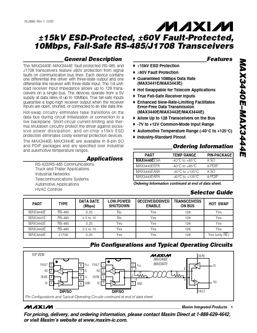
General DescriptionThe MAX3440E–MAX3444E fault-protected RS-485 and J1708 transceivers feature ±60V protection from signal faults on communication bus lines. Each device contains one differential line driver with three-state output and one differential line receiver with three-state input. The 1/4-unit-load receiver input impedance allows up to 128 trans-ceivers on a single bus. The devices operate from a 5V supply at data rates of up to 10Mbps. True fail-safe inputs guarantee a logic-high receiver output when the receiver inputs are open, shorted, or connected to an idle data line.Hot-swap circuitry eliminates false transitions on the data bus during circuit initialization or connection to a live backplane. Short-circuit current-limiting and ther-mal shutdown circuitry protect the driver against exces-sive power dissipation, and on-chip ±15kV ESD protection eliminates costly external protection devices.The MAX3440E–MAX3444E are available in 8-pin SO and PDIP packages and are specified over industrial and automotive temperature ranges.ApplicationsRS-422/RS-485 Communications Truck and Trailer Applications Industrial NetworksTelecommunications Systems Automotive Applications Features♦±15kV ESD Protection ♦±60V Fault Protection♦Guaranteed 10Mbps Data Rate (MAX3441E/MAX3443E)♦Hot Swappable for Telecom Applications ♦True Fail-Safe Receiver Inputs♦Enhanced Slew-Rate-Limiting Facilitates Error-Free Data Transmission(MAX3440E/MAX3442E/MAX3444E)♦Allow Up to 128 Transceivers on the Bus ♦-7V to +12V Common-Mode Input Range♦Automotive Temperature Range (-40°C to +125°C)♦Industry-Standard PinoutMAX3440E–MAX3444E±15kV ESD-Protected, ±60V Fault-Protected,10Mbps, Fail-Safe RS-485/J1708 Transceivers________________________________________________________________Maxim Integrated Products 1Pin Configurations and Typical Operating CircuitsOrdering Information19-2666; Rev 1; 12/05For pricing, delivery, and ordering information, please contact Maxim Direct at 1-888-629-4642,or visit Maxim’s website at .Ordering Information continued at end of data sheet.M A X 3440E –M A X 3444E±15kV ESD-Protected, ±60V Fault-Protected,10Mbps, Fail-Safe RS-485/J1708 Transceivers 2_______________________________________________________________________________________ABSOLUTE MAXIMUM RATINGSStresses beyond those listed under “Absolute Maximum Ratings” may cause permanent damage to the device. These are stress ratings only, and functional operation of the device at these or any other conditions beyond those indicated in the operational sections of the specifications is not implied. Exposure to absolute maximum rating conditions for extended periods may affect device reliability.Voltages Referenced to GNDV CC ........................................................................................+7V FAULT, DE/RE, RE , DE, DE , DI, TXD..........-0.3V to (V CC + 0.3V)A, B (Note 1)........................................................................±60V RO..............................................................-0.3V to (V CC + 0.3V)Short-Circuit Duration (RO, A, B)...............................Continuous Continuous Power Dissipation (T A = +70°C)8-Pin SO (derate 5.9mW/°C above +70°C)..................471mW 8-Pin PDIP (derate 9.09mW/°C above +70°C).............727mWOperating Temperature RangesMAX344_EE_ _...............................................-40°C to +85°C MAX344_EA_ _.............................................-40°C to +125°C Storage Temperature Range.............................-65°C to +150°C Junction Temperature......................................................+150°C Lead Temperature (soldering, 10s).................................+300°CDC ELECTRICAL CHARACTERISTICSNote 1:A, B must be terminated with 54Ωor 100Ωto guarantee ±60V fault protection.MAX3440E–MAX3444E±15kV ESD-Protected, ±60V Fault-Protected,10Mbps, Fail-Safe RS-485/J1708 TransceiversDC ELECTRICAL CHARACTERISTICS (continued)(V = +4.75V to +5.25V, T = T to T , unless otherwise noted. Typical values are at V = +5V and T = +25°C.)M A X 3440E –M A X 3444E±15kV ESD-Protected, ±60V Fault-Protected,10Mbps, Fail-Safe RS-485/J1708 Transceivers 4_______________________________________________________________________________________SWITCHING CHARACTERISTICS (MAX3440E/MAX3442E/MAX3444E)MAX3440E–MAX3444E±15kV ESD-Protected, ±60V Fault-Protected,10Mbps, Fail-Safe RS-485/J1708 Transceivers_______________________________________________________________________________________5SWITCHING CHARACTERISTICS (MAX3441E/MAX3443E)(V CC = +4.75V to +5.25V, T A = T MIN to T MAX , unless otherwise noted. Typical values are at V CC = +5V and T A = +25°C.)Note 3:The short-circuit output current applies to peak current just before foldback current limiting; the short-circuit foldback outputcurrent applies during current limiting to allow a recovery from bus contention.M A X 3440E –M A X 3444E±15kV ESD-Protected, ±60V Fault-Protected,10Mbps, Fail-Safe RS-485/J1708 Transceivers 6_______________________________________________________________________________________RECEIVER OUTPUT CURRENT vs. OUTPUT LOW VOLTAGEM A X 3443E t o c 04OUTPUT LOW VOLTAGE (V)R E C E I V E R O U T P U T C U R R E N T (m A )5.04.50.5 1.0 1.5 2.5 3.0 3.52.0 4.051015202530354000RECEIVER OUTPUT CURRENT vs. OUTPUT HIGH VOLTAGEM A X 3443E t o c 05OUTPUT HIGH VOLTAGE (V)R E C E I V E R O U T P U T C U R R E N T (m A )5.04.50.5 1.0 1.5 2.5 3.0 3.52.0 4.051015202530354000RECEIVER OUTPUT VOLTAGEvs. TEMPERATURETEMPERATURE (°C)R E C E I V E R O U T P U T V O L T A G E (V )110956580-105203550-250.51.01.52.02.53.03.54.04.55.0-40125DRIVER OUTPUT CURRENTvs. DIFFERENTIAL OUTPUT VOLTAGEDIFFERENTIAL OUTPUT VOLTAGE (V A - V B ) (V)D R I VE R O U T P U T C U R R E N T (m A )0.51.0 1.52.53.0 3.52.010203040506070800DIFFERENTIAL OUTPUT VOLTAGEvs. TEMPERATURETEMPERATURE (°C)D I F FE R E N T I A L O U T P U T V O L T A G E (V )110956580-105203550-250.51.01.52.02.53.03.50-40125Typical Operating Characteristics(V CC = +5V, T A = +25°C, unless otherwise noted.)NO-LOAD SUPPLY CURRENTvs. TEMPERATURETEMPERATURE (°C)S U P P L Y C U R R E N T (m A )1109580655035205-10-251234560-40125NO-LOAD SUPPLY CURRENTvs. TEMPERATURETEMPERATURE (°C)S U P P L Y C U R R E N T (m A )1109580655035205-10-2548121620240-40125SHUTDOWN SUPPLY CURRENTvs. TEMPERATURETEMPERATURE (°C)S U P P L Y C U R R E N T (μA )1109580655035205-10-250.11100.01-40125A, B CURRENTvs. A, B VOLTAGE (TO GROUND)A, B VOLTAGE (V)A ,BC U R R E N T (μA )40306050-50-40-30-10010-2020-800-400-1600-2000-12000400800120016002000-60MAX3440E–MAX3444E±15kV ESD-Protected, ±60V Fault-Protected,10Mbps, Fail-Safe RS-485/J1708 TransceiversOD OCFigure 3. Driver Propagation TimesTest Circuits and WaveformsM A X 3440E –M A X 3444E±15kV ESD-Protected, ±60V Fault-Protected,10Mbps, Fail-Safe RS-485/J1708 Transceivers 8_______________________________________________________________________________________Figure 7. Receiver Propagation DelayFigure 5. Driver Enable and Disable TimesMAX3440E–MAX3444E±15kV ESD-Protected, ±60V Fault-Protected,10Mbps, Fail-Safe RS-485/J1708 Transceivers_______________________________________________________________________________________9Note 4:The input pulse is supplied by a generator with the following characteristics: f = 5MHz, 50% duty cycle; tr ≤6ns; Z 0= 50Ω.Note 5:C L includes probe and stray capacitance.M A X 3440E –M A X 3444E±15kV ESD-Protected, ±60V Fault-Protected,10Mbps, Fail-Safe RS-485/J1708 Transceivers 10______________________________________________________________________________________MAX3440E–MAX3444E±15kV ESD-Protected, ±60V Fault-Protected,10Mbps, Fail-Safe RS-485/J1708 Transceivers______________________________________________________________________________________11Table 5. MAX3440E/MAX3441E (RS-485/RS-422)Detailed DescriptionThe MAX3440E–MAX3444E fault-protected transceivers for RS-485/RS-422 and J1708 communication contain one driver and one receiver. These devices feature fail-safe circuitry, which guarantees a logic-high receiver output when the receiver inputs are open or shorted, or when they are connected to a terminated transmission line with all drivers disabled (see the True Fail-Safe section). All devices have a hot-swap input structure that prevents disturbances on the differential signal lines when a circuit board is plugged into a hot back-plane (see the Hot-Swap Capability section). The MAX3440E/MAX3442E/MAX3444E feature a reduced slew-rate driver that minimizes EMI and reduces reflec-tions caused by improperly terminated cables, allowing error-free data transmission up to 250kbps (see the Reduced EMI and Reflections section). The MAX3441E/MAX3443E drivers are not slew-rate limited, allowing transmit speeds up to 10Mbps.DriverThe driver accepts a single-ended, logic-level input (DI) and transfers it to a differential, RS-485/RS-422level output (A and B). Deasserting the driver enable places the driver outputs (A and B) into a high-imped-ance state.ReceiverThe receiver accepts a differential, RS-485/RS-422level input (A and B), and transfers it to a single-ended,logic-level output (RO). Deasserting the receiver enable places the receiver inputs (A and B) into a high-imped-ance state (see Tables 1–7).Low-Power Shutdown(MAX3442E/MAX3443E/MAX3444E)The MAX3442E/MAX3443E/MAX3444E offer a low-power shutdown mode. Force DE low and RE high to shut down the MAX3442E/MAX3443E. Force DE and RE high to shut down the MAX3444E. A time delay of 50ns prevents the device from accidentally entering shutdown due to logic skews when switching between transmit and receive modes. Holding DE low and RE high for at least 800ns guarantees that the MAX3442E/MAX3443E enter shutdown. In shutdown, the devices consume a maxi-mum 20µA supply current.±60V Fault ProtectionThe driver outputs/receiver inputs of RS-485 devices in industrial network applications often experience voltage faults resulting from shorts to the power grid that exceed the -7V to +12V range specified in the EIA/TIA-485 standard. In these applications, ordinary RS-485devices (typical absolute maximum -8V to +12.5V)require costly external protection devices. To reduce system complexity and eliminate this need for external protection, the driver outputs/receiver inputs of the MAX3440E–MAX3444E withstand voltage faults up to ±60V with respect to ground without damage.Protection is guaranteed regardless whether the device is active, shut down, or without power.True Fail-SafeThe MAX3440E–MAX3444E use a -50mV to -200mV differential input threshold to ensure true fail-safe receiver inputs. This threshold guarantees the receiver outputs a logic high for shorted, open, or idle data lines. The -50mV to -200mV threshold complies with the ±200mV threshold EIA/TIA-485 standard.M A X 3440E –M A X 3444E±15kV ESD-Protected, ±60V Fault-Protected,10Mbps, Fail-Safe RS-485/J1708 Transceivers 12______________________________________________________________________________________±15kV ESD ProtectionAs with all Maxim devices, ESD-protection structures are incorporated on all pins to protect against ESD encountered during handling and assembly. The MAX3440E–MAX3444E receiver inputs/driver outputs (A, B) have extra protection against static electricity found in normal operation. Maxim’s engineers have developed state-of-the-art structures to protect these pins against ±15kV ESD without damage. After an ESD event, the MAX3440E–MAX3444E continue working without latchup.ESD protection can be tested in several ways. The receiver inputs are characterized for protection to ±15kV using the Human Body Model.ESD Test ConditionsESD performance depends on a number of conditions.Contact Maxim for a reliability report that documents test setup, methodology, and results.Human Body ModelFigure 9a shows the Human Body Model, and Figure 9b shows the current waveform it generates when dis-charged into a low impedance. This model consists of a 100pF capacitor charged to the ESD voltage of inter-est, which is then discharged into the device through a 1.5k Ωresistor.Driver Output ProtectionTwo mechanisms prevent excessive output current and power dissipation caused by faults or bus contention.The first, a foldback current limit on the driver output stage, provides immediate protection against short cir-cuits over the whole common-mode voltage range. The second, a thermal shutdown circuit, forces the driver out-puts into a high-impedance state if the die temperature exceeds +160°C. Normal operation resumes when the die temperature cools to +140°C, resulting in a pulsed output during continuous short-circuit conditions.MAX3440E–MAX3444E±15kV ESD-Protected, ±60V Fault-Protected,10Mbps, Fail-Safe RS-485/J1708 Transceivers______________________________________________________________________________________13Figure 9a. Human Body ESD Test ModelM A X 3440E –M A X 3444E±15kV ESD-Protected, ±60V Fault-Protected,10Mbps, Fail-Safe RS-485/J1708 Transceivers 14______________________________________________________________________________________Hot-Swap CapabilityHot-Swap InputsInserting circuit boards into a hot, or powered, back-plane may cause voltage transients on DE, DE/RE, RE ,and receiver inputs A and B that can lead to data errors.For example, upon initial circuit board insertion, the processor undergoes a power-up sequence. During this period, the high-impedance state of the output drivers makes them unable to drive the MAX3440E–MAX3444E enable inputs to a defined logic level. Meanwhile, leak-age currents of up to 10µA from the high-impedance out-put, or capacitively coupled noise from V CC or G ND,could cause an input to drift to an incorrect logic state.To prevent such a condition from occurring, the MAX3440E–MAX3443E feature hot-swap input circuitry on DE, DE/RE, and RE to guard against unwanted dri-ver activation during hot-swap situations. The MAX3444E has hot-swap input circuitry only on RE .When V CC rises, an internal pulldown (or pullup for RE )circuit holds DE low for at least 10µs, and until the cur-rent into DE exceeds 200µA. After the initial power-up sequence, the pulldown circuit becomes transparent,resetting the hot-swap tolerable input.Hot-Swap Input CircuitryAt the driver-enable input (DE), there are two NMOS devices, M1 and M2 (Figure 10). When V CC ramps from zero, an internal 15µs timer turns on M2 and sets the SR latch, which also turns on M1. Transistors M2, a 2mA current sink, and M1, a 100µA current sink, pull DE to GND through a 5.6k Ωresistor. M2 pulls DE to the disabled state against an external parasitic capaci-tance up to 100pF that may drive DE high. After 15µs,the timer deactivates M2 while M1 remains on, holding DE low against three-state leakage currents that may drive DE high. M1 remains on until an external current source overcomes the required input current. At this time, the SR latch resets M1 and turns off. When M1turns off, DE reverts to a standard, high-impedance CMOS input. Whenever V CC drops below 1V, the input is reset.A complementary circuit for RE uses two PMOS devices to pull RE to V CC .__________Applications Information128 Transceivers on the BusThe MAX3440E–MAX3444E transceivers 1/4-unit-load receiver input impedance (48k Ω) allows up to 128transceivers connected in parallel on one communica-tion line. Connect any combination of these devices,and/or other RS-485 devices, for a maximum of 32-unit loads to the line.Reduced EMI and ReflectionsThe MAX3440E/MAX3442E/MAX3444E are slew-rate limited, minimizing EMI and reducing reflections caused by improperly terminated cables. Figure 11shows the driver output waveform and its Fourier analy-sis of a 125kHz signal transmitted by a MAX3443E.High-frequency harmonic components with large ampli-tudes are evident.Figure 12 shows the same signal displayed for a MAX3442E transmitting under the same conditions.Figure 12’s high-frequency harmonic components are much lower in amplitude, compared with Figure 11’s,and the potential for EMI is significantly reduced.Figure 10. Simplified Structure of the Driver Enable Pin (DE)In general, a transmitter’s rise time relates directly to the length of an unterminated stub, which can be dri-ven with only minor waveform reflections. The following equation expresses this relationship conservatively:Length = t RISE / (10 x 1.5ns/ft)where t RISE is the transmitter’s rise time.For example, the MAX3442E’s rise time is typically 800ns, which results in excellent waveforms with a stub length up to 53ft. A system can work well with longer unterminated stubs, even with severe reflections, if the waveform settles out before the UART samples them.RS-485 ApplicationsThe MAX3440E–MAX3443E transceivers provide bidi-rectional data communications on multipoint bus trans-mission lines. Figures 13 and 14show a typical network applications circuit. The RS-485 standard covers line lengths up to 4000ft. To minimize reflections and reduce data errors, terminate the signal line at both ends in its characteristic impedance, and keep stub lengths off the main line as short as possible.J1708 ApplicationsThe MAX3444E is designed for J1708 applications. To configure the MAX3444E, connect DE and RE to G ND.Connect the signal to be transmitted to TXD. Terminate the bus with the load circuit as shown in Figure 15. The drivers used by SAE J1708 are used in a dominant-mode application. DE is active low; a high input on DE places the outputs in high impedance. When the driver is disabled (TXD high or DE high), the bus is pulled high by external bias resistors R1 and R2. Therefore, a logic level high is encoded as recessive. When all transceivers are idle in this configuration, all receivers output logic high because of the pullup resistor on A and pulldown resistor on B. R1 and R2 provide the bias for the recessive state.C1 and C2 combine to form a 6MHz lowpass filter, effec-tive for reducing FM interference. R2, C1, R4, and C2combine to form a 1.6MHz lowpass filter, effective for reducing AM interference. Because the bus is untermi-nated, at high frequencies, R3 and R4 perform a pseudotermination. This makes the implementation more flexible, as no specific termination nodes are required at the ends of the bus.MAX3440E–MAX3444E±15kV ESD-Protected, ±60V Fault-Protected,10Mbps, Fail-Safe RS-485/J1708 Transceivers______________________________________________________________________________________155.00MHz 500kHz/div 020dB/div Figure 11. Driver Output Waveform and FFT Plot of MAX3443E Transmitting a 125kHz Signal 5.00MHz500kHz/div 020dB/divFigure 12. Driver Output Waveform and FFT Plot of MAX3442E Transmitting a 125kHz SignalM A X 3440E –M A X 3444E±15kV ESD-Protected, ±60V Fault-Protected,10Mbps, Fail-Safe RS-485/J1708 Transceivers 16______________________________________________________________________________________Figure 13. MAX3440E/MAX3441E Typical RS-485 NetworkFigure 14. MAX3442E/MAX3443E Typical RS-485 NetworkMAX3440E–MAX3444E±15kV ESD-Protected, ±60V Fault-Protected,10Mbps, Fail-Safe RS-485/J1708 TransceiversFigure 15. J1708 Application CircuitChip InformationTRANSISTOR COUNT: 310PROCESS: BiCMOSPin Configurations and Typical Operating Circuits (continued)M A X 3440E –M A X 3444E±15kV ESD-Protected, ±60V Fault-Protected,10Mbps, Fail-Safe RS-485/J1708 Transceivers 18______________________________________________________________________________________Ordering Information (continued)MAX3440E–MAX3444E±15kV ESD-Protected, ±60V Fault-Protected,10Mbps, Fail-Safe RS-485/J1708 Transceivers______________________________________________________________________________________19Package Information(The package drawing(s) in this data sheet may not reflect the most current specifications. For the latest package outline information,go to /packages .)M A X 3440E –M A X 3444E±15kV ESD-Protected, ±60V Fault-Protected,10Mbps, Fail-Safe RS-485/J1708 Transceivers Maxim cannot assume responsibility for use of any circuitry other than circuitry entirely embodied in a Maxim product. N o circuit patent licenses are implied. Maxim reserves the right to change the circuitry and specifications without notice at any time.20____________________Maxim Integrated Products, 120 San Gabriel Drive, Sunnyvale, CA 94086 408-737-7600©2005 Maxim Integrated ProductsPrinted USAis a registered trademark of Maxim Integrated Products.Package Information (continued)(The package drawing(s) in this data sheet may not reflect the most current specifications. For the latest package outline information,go to /packages .)____________________Revision HistoryPages changed at Rev 1: 1, 6, 11。
MAX3301EETJ中文资料
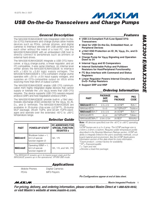
General DescriptionThe MAX3301E/MAX3302E fully integrated USB On-the-Go (OTG) transceivers and charge pumps allow mobile devices such as PDAs, cellular phones, and digital cameras to interface directly with USB peripherals and each other without the need of a host PC. Use the MAX3301E/MAX3302E with an embedded USB host to directly connect to peripherals such as printers or external hard drives.The MAX3301E/MAX3302E integrate a USB OTG trans-ceiver, a V BUS charge pump, a linear regulator, and an I 2C-compatible, 2-wire serial interface. An internal level shifter allows the MAX3301E/MAX3302E to interface with +1.65V to +3.6V logic supply voltages. The MAX3301E/MAX3302E’s OTG-compliant charge pump operates with +3V to +4.5V input supply voltages, and supplies an OTG-compatible output on V BUS while sourcing more than 8mA of output current.The MAX3301E/MAX3302E enable USB OTG communi-cation from highly integrated digital devices that cannot supply or tolerate the +5V V BUS levels that USB OTG requires. The device supports USB OTG session-request protocol (SRP) and host-negotiation protocol (HNP).The MAX3301E/MAX3302E provide built-in ±15kV elec-trostatic-discharge (ESD) protection for the V BUS , ID_IN,D+, and D- terminals. The MAX3301E/MAX3302E are available in 25-bump chip-scale (UCSP™), 25-bump WLP package, 28-pin TQF N, and 32-pin TQF N pack-ages and operate over the extended -40°C to +85°C temperature range.ApplicationsMobile Phones Digital Cameras PDAsMP3 PlayersFeatureso USB 2.0-Compliant Full-/Low-Speed OTG Transceiverso Ideal for USB On-the-Go, Embedded Host, or Peripheral Deviceso ±15kV ESD Protection on ID_IN, V BUS , D+, and D-Terminalso Charge Pump for V BUS Signaling and Operation Down to 3Vo Internal V BUS and ID Comparatorso Internal Switchable Pullup and Pulldown Resistors for Host/Peripheral Functionality o I 2C Bus Interface with Command and Status Registerso Linear Regulator Powers Internal Circuitry and D+/D- Pullup Resistors o Support SRP and HNPMAX3301E/MAX3302EUSB On-the-Go Transceivers and Charge Pumps________________________________________________________________Maxim Integrated Products1Ordering Information19-3275; Rev 3; 10/07For pricing, delivery, and ordering information,please contact Maxim Direct at 1-888-629-4642,or visit Maxim’s website at .Note:All devices specified over the -40°C to +85°C operating range.‡UCSP bumps are in a 5 x 5 array. The UCSP package size is 2.5mm x 2.5mm x 0.62mm. Requires solder temperature profile described in the Absolute Maximum Ratings section. UCSP reli-ability is integrally linked to the user’s assembly methods, circuit board material and environment. See the UCSP Applications Information section of this data sheet for more information.*Future product—contact factory for availability.**EP = Exposed paddle.T = Tape and reel.+Denotes a lead-free package.Selector GuidePin Configurations appear at end of data sheet.M A X 3301E /M A X 3302EUSB On-the-Go Transceivers and Charge PumpsABSOLUTE MAXIMUM RATINGSDC ELECTRICAL CHARACTERISTICS(V CC = +3V to +4.5V, V L = +1.65V to +3.6V, C FLYING = 100nF, C VBUS = 1µF, ESR CVBUS = 0.1Ω(max), T A = T MIN to T MAX , unless otherwise noted. Typical values are at V CC = +3.7V, V L = +2.5V, T A = +25°C.) (Note 2)Note 1:The UCSP package is constructed using a unique set of packaging techniques that impose a limit on the thermal profile the device can be exposed to during board-level solder attach and rework. This limit permits only the use of the solder profiles recom-mended in the industry-standard specification, JEDEC 020A, paragraph 7.6, Table 3 for IR/VPR and convection reflow. Preheating is required. Hand or wave soldering is not allowed.Stresses beyond those listed under “Absolute Maximum Ratings” may cause permanent damage to the device. These are stress ratings only, and functional operation of the device at these or any other conditions beyond those indicated in the operational sections of the specifications is not implied. Exposure to absolute maximum rating conditions for extended periods may affect device reliability.All voltages are referenced to GND.V CC , V L .....................................................................-0.3V to +6V TRM (regulator off or supplied by V BUS )..-0.3V to (V BUS + 0.3V)TRM (regulator supplied by V CC )...............-0.3V to (V CC + 0.3V)D+, D- (transmitter tri-stated)...................................-0.3V to +6V D+, D- (transmitter functional)....................-0.3V to (V CC + 0.3V)V BUS .........................................................................-0.3V to +6V ID_IN, SCL, SDA.......................................................-0.3V to +6V INT , SPD, RESET , ADD, OE/INT , RCV, VP,VM, SUS, DAT_VP, SE0_VM ......................-0.3V to (V L + 0.3V)C+.............................................................-0.3V to (V BUS + 0.3V)C-................................................................-0.3V to (V CC + 0.3V)Short-Circuit Duration, V BUS to GND .........................ContinuousContinuous Power Dissipation (T A = +70°C)25-Bump WLP (derate 12.2mW/°C above +70°C).......976mW 25-Bump UCSP (derate 12.2mW/°C above +70°C)....976mW 32-Pin TQFN (5mm x 5mm x 0.8mm) (derate 21.3mW/°Cabove +70°C).........................................................1702mW 28-Pin TQFN (4mm x 4mm x 0.8mm) (derate 20.8mW/°Cabove +70°C).........................................................1666mW Operating Temperature Range ...........................-40°C to +85°C Junction Temperature......................................................+150°C Storage Temperature Range.............................-65°C to +150°C Lead Temperature (soldering, 10s).................................+300°C Bump Reflow Temperature (Note 1)Infrared (15s)...............................................................+200°C Vapor Phase (20s).......................................................+215°CM MMAX3301E/MAX3302EUSB On-the-Go Transceivers and Charge Pumps_______________________________________________________________________________________3DC ELECTRICAL CHARACTERISTICS (continued)(V CC = +3V to +4.5V, V L = +1.65V to +3.6V, C FLYING = 100nF, C VBUS = 1µF, ESR CVBUS = 0.1Ω(max), T A = T MIN to T MAX , unless otherwise noted. Typical values are at V CC = +3.7V, V L = +2.5V, T A = +25°C.) (Note 2)M A X 3301E /M A X 3302EUSB On-the-Go Transceivers and Charge Pumps 4_______________________________________________________________________________________DC ELECTRICAL CHARACTERISTICS (continued)(V CC = +3V to +4.5V, V L = +1.65V to +3.6V, C FLYING = 100nF, C VBUS = 1µF, ESR CVBUS = 0.1Ω(max), T A = T MIN to T MAX , unless otherwise noted. Typical values are at V CC = +3.7V, V L = +2.5V, T A = +25°C.) (Note 2)MAX3301E/MAX3302EUSB On-the-Go Transceivers and Charge Pumps_______________________________________________________________________________________5TIMING CHARACTERISTICSM A X 3301E /M A X 3302EUSB On-the-Go Transceivers and Charge Pumps 6_______________________________________________________________________________________I 2C-/SMBus™-COMPATIBLE TIMING SPECIFICATIONSNote 3:Guaranteed by bench characterization. Limits are not production tested.Note 4:A master device must provide a hold time of at least 300ns for the SDA signal to bridge the undefined region of SCL’s fallingedge.Note 5:C B is the total capacitance of one bus line in pF, tested with C B = 400pF.Note 6:Input filters on SDA, SCL, and ADD suppress noise spikes of less than 50ns.SMBus is a trademark of Intel Corporation.DRIVER PROPAGATION DELAY HIGH-TO-LOW(FULL-SPEED MODE)MAX3301E toc094ns/divD+1V/divD-1V/divDAT_VP 1V/divDRIVER PROPAGATION DELAY LOW-TO-HIGH(LOW-SPEED MODE)MAX3301E toc08100ns/divD-1V/divD+1V/div DAT_VP 1V/div DRIVER PROPAGATION DELAY HIGH-TO-LOW(LOW-SPEED MODE)MAX3301E toc07100ns/divD+1V/divD-1V/divDAT_VP 1V/div TIME TO EXIT SHUTDOWNMAX3301E toc054μs/div D-1V/divD+1V/divSCL 1V/divV BUS DURING SRP20ns/divV BUS 1V/divV BUS 1V/divC VBUS > 96μFC VBUS > 13μFTIME TO ENTER SHUTDOWNMAX3301E toc04100ns/div D+1V/div D-1V/div SCL 2V/div V BUS OUTPUT VOLTAGE vs. INPUT VOLTAGE (V CC )INPUT VOLTAGE (V CC ) (V)V B U S O U T P U T V O L T A G E (V )5.55.04.54.03.53.04.755.005.255.505.754.502.56.0V BUS OUTPUT VOLTAGE vs. VBUS OUTPUT CURRENTV BUS OUTPUT CURRENT (mA)V B U S O U T P U T V O L T A G E (V )2520151054.254.504.755.005.255.504.0030INPUT CURRENT (ICC )vs. V BUS OUTPUT CURRENTV BUS OUTPUT CURRENT (mA)I N P U T C U R R E N T (I C C ) (m A )16128410203040500020MAX3301E/MAX3302EUSB On-the-Go Transceivers and Charge Pumps_______________________________________________________________________________________7Typical Operating Characteristics(Typical operating circuit, V CC = +3.7V, V L = +2.5V, C FLYING = 100nF, T A = +25°C, unless otherwise noted.)SUPPLY CURRENT vs. TEMPERATURETEMPERATURE (°C)S U P P L Y C U R R E N T (m A )603510-150.20.40.60.81.00-4085DRIVER DISABLE DELAY (LOW-SPEED MODE)MAX3301E toc1410ns/divD+1V/divD-1V/divOE/INT 1V/divDRIVER ENABLE DELAY (LOW-SPEED MODE)MAX3301E toc13100ns/divD-1V/divD+1V/div C D+ = C D- = 400pFOE/INT 1V/divDRIVER DISABLE DELAY (FULL-SPEED MODE)MAX3301E toc1210ns/divD+1V/divD-1V/divOE/INT 1V/divDRIVER ENABLE DELAY (FULL-SPEED MODE)MAX3301E toc1110ns/divD-1V/divD+1V/div OE/INT 1V/divDRIVER PROPAGATION DELAY LOW-TO-HIGH(FULL-SPEED MODE)MAX3301E toc104ns/divD-1V/divD+1V/divDAT_VP 1V/div M A X 3301E /M A X 3302EUSB On-the-Go Transceivers and Charge Pumps 8_______________________________________________________________________________________Typical Operating Characteristics (continued)(Typical operating circuit, V CC = +3.7V, V L = +2.5V, C FLYING = 100nF, T A = +25°C, unless otherwise noted.)MAX3301E/MAX3302EUSB On-the-Go Transceivers and Charge PumpsM A X 3301E /M A X 3302EUSB On-the-Go Transceivers and Charge Pumps 10______________________________________________________________________________________Test Circuits and Timing DiagramsFigure 1. Load for Disable Time MeasurementFigure 2. Load for Enable Time, Transmitter Propagation Delay,and Transmitter Rise/Fall TimesMAX3301E/MAX3302EUSB On-the-Go Transceivers and Charge PumpsTest Circuits and Timing Diagrams (continued)Figure 6. Timing of DAT_VP, SE0_VM to D+, D- in VP_VM Mode (dat_se0 = 0)Figure 7. Timing of DAT_VP, SE0_VM to D+/D- in DAT_SE0Mode (dat_se0 = 1)Figure 8. Enable and Disable TimingFigure 9. D+/D- to RCV, DAT_VP, SE0_VM Propagation Delays(VP_VM Mode)Figure 10. D+/D- to DAT_VP, SE0_VM Propagation Delays (DAT_SE0 Mode)Figure 3. Load for Receiver Propagation Delay and Receiver Rise/Fall TimesFigure 4. Load for DAT_VP, SE0_VM Enable/Disable Time MeasurementsM A X 3301E /M A X 3302EUSB On-the-Go Transceivers and Charge Pumps Block DiagramFigure 11. Block DiagramMAX3301E/MAX3302EUSB On-the-Go Transceivers and Charge PumpsDetailed DescriptionThe USB OTG specification defines a dual-role USB device that acts either as an A device or as a B device.The A device supplies power on V BUS and initially serves as the USB host. The B device serves as the ini-tial peripheral and requires circuitry to monitor and pulse V BUS . These initial roles can be reversed using HNP.The MAX3301E/MAX3302E combine a low- and full-speed USB transceiver with additional circuitry required by a dual-role device. The MAX3301E/MAX3302E employ flexible switching circuitry to enable the device to act as a dedicated host or peripheral USB transceiv-er. For example, the charge pump can be turned off and the internal regulator can be powered from V BUS for bus-powered peripheral applications.The Selector Guide shows the differences between the MAX3301E and MAX3302E. The MAX3301E powers up in its lowest power state and must be turned on by set-ting the sdwn bit to 0. The MAX3302E powers up in the operational, VP/VM USB mode. This allows a micro-processor (µP) to use the USB port for power-on boot-up, without having to access I 2C. To put the MAX3302E into low-power shutdown, set the sdwn bit to 0. In the MAX3302E, special-function register 2 can be addressed at I 2C register location 10h, 11h (as well as locations 16h, 17h) to support USB OTG serial-interface engine (SIE) implementations that are limited to I 2C register addresses between 0h and 15h.TransceiverThe MAX3301E/MAX3302E transceiver complies with the USB version 2.0 specification, and operates at full-speed (12Mbps) and low-speed (1.5Mbps) data rates.Set the data rate with the SPD input. Set the direction of data transfer with the OE/INT input. Alternatively, control transceiver operation with control register 1 (Table 7)and special-function registers 1 and 2 (see Tables 14,15, and 16).Level ShiftersInternal level shifters allow the system-side interface to run at logic-supply voltages as low as +1.65V. Interface logic signals are referenced to the voltage applied to the logic-supply voltage, V L .Charge PumpThe MAX3301E/MAX3302E’s OTG-compliant charge pump operates with +3V to +4.5V input supply voltages (V CC ) and supplies a +4.8V to +5.25V OTG-compatible output on V BUS while sourcing the 8mA or greater out-put current that an A device is required to supply.Connect a 0.1µF flying capacitor between C+ and C-.Bypass V BUS to GND with a 1µF to 6.5µF capacitor, inaccordance with USB OTG specifications. The charge pump can be turned off to conserve power when not used. Control of the charge pump is set through the vbus_drv bit (bit 5) of control register 2 (see Table 8).Linear Regulator (TRM)An internal 3.3V linear regulator powers the transceiver and the internal 1.5k ΩD+/D- pullup resistor. Under the control of internal register bits, the linear regulator can be powered from V CC or V BUS . The regulator power-supply settings are controlled by the reg_sel bit (bit 3) in special-function register 2 (Tables 15 and 16). This flexibility allows the system designer to configure the MAX3301E/MAX3302E for virtually any USB power situation.The output of the TRM is not a power supply. Do not use as a power source for any external circuitry. Connect a 1.0µF (or greater) ceramic or plastic capacitor from TRM to GND, as close to the device as possible.V BUS Level-Detection ComparatorsComparators drive interrupt source register bits 0, 1,and 7 (Table 10) to indicate important USB OTG V BUS voltage levels:•V BUS is valid (vbus_vld)•USB session is valid (sess_vld)•USB session has ended (sess_end)The vbus_valid comparator sets vbus_vld to 1 if V BUS is higher than the V BUS valid comparator threshold. The V BUS valid status bit (vbus_vld) is used by the A device to determine if the B device is sinking too much current (i.e., is not supported). The session_valid comparator sets sess_vld to 1 if V BUS is higher than the session valid comparator threshold. This status bit indicates that a data transfer session is valid. The session_end com-parator sets sess_end to 1 if V BUS is higher than theFigure 12. Comparator Network DiagramM A X 3301E /M A X 3302EUSB On-the-Go Transceivers and Charge Pumpssession end comparator threshold. Figure 12 shows the level-detector comparators. The interrupt-enable regis-ters (Tables 12 and 13) determine whether a falling or rising edge of V BUS asserts these status bits.ID_INThe USB OTG specification defines an ID input that determines which dual-role device is the default host.An OTG cable connects ID to ground in the connector of one end and is left unconnected in the other end.Whichever dual-role device receives the grounded end becomes the A device. The MAX3301E/MAX3302E pro-vide an internal pullup resistor on ID_IN. Internal com-parators detect if ID_IN is grounded or left floating.Interrupt LogicWhen OTG events require action, the MAX3301E/MAX3302E provide an interrupt output signal on INT .Alternatively, OE/INT can be configured to act as an interrupt output while the device operates in USB sus-pend mode. Program INT and OE/INT as open-drain or push-pull interrupts with irq_mode (bit 1 of special-func-tion register 2, see Tables 15 and 16).V BUS Power ControlV BUS is a dual-function port that powers the USB bus and/or provides a power source for the internal linear reg-ulator. The V BUS power-control block performs the various switching functions required by an OTG dual-role device.These actions are programmed by the system logic using bits 5 to 7 of control register 2 (see Table 8) to:•Discharge V BUS through a resistor•Provide power-on or receive power from V BUS •Charge V BUS through a resistorThe OTG supplement allows an A device to turn V BUS off when the bus is not being used to conserve power.The B device can issue a request that a new session be started using SRP. The B device must discharge V BUS to a level below the session-end threshold (0.8V) to ensure that no session is in progress before initiating SRP. Setting bit 6 of control register 2 to 1, discharges V BUS to GND through a 5k Ωcurrent-limiting resistor.When V BUS has discharged, the resistor is removed from the circuit by resetting bit 6 of control register 2. An OTG A device is required to supply power on V BUS .The MAX3301E/MAX3302E provide power to V BUS from V CC or from the internal charge pump. Set bit 5 in control register 2 to 1 in both cases. Bit 5 in control register 2controls a current-limited switch, preventing damage to the device in the event of a V BUS short circuit.An OTG B device (peripheral mode) can request a ses-sion using SRP. One of the steps in implementing SRP requires pulsing V BUS high for a controlled time. A 930Ωresistor limits the current according to the OTG specifi-cation. Pulse V BUS through the pullup resistor by assert-ing bit 7 of control register 2. Prior to pulsing V BUS (bit 7), a B device first connects an internal pulldown resis-tor to discharge V BUS below the session-end threshold.The discharge current is limited by the 5k Ωresistor and set by bit 6 of control register 2. An OTG A device mustMAX3301E/MAX3302EUSB On-the-Go Transceivers and Charge Pumpssupply 5V power and at least 8mA on V BUS . Setting bit 5 of control register 2 turns on the V BUS charge pump.Operating ModesThe MAX3301E/MAX3302E have four operating modes to optimize power consumption. Only the I 2C interface remains active in shutdown mode, reducing supply cur-rent to 1µA. The I 2C interface, the ID_IN port, and the session-valid comparator all remain active in interrupt shutdown mode. RCV asserts low in suspend mode; how-ever, all other circuitry remains active. Table 1 lists the active blocks’ power in each of the operating modes.Applications InformationData TransferTransmitting Data to the USBThe MAX3301E/MAX3302E transceiver features two modes of transmission: DAT_SE0 or VP_VM (see Table 3).Set the transmitting mode with dat_se0 (bit 2 in control register 1, see Table 7). In DAT_SE0 mode with OE/INT low, DAT_VP specifies data for the differential transceiv-er, and SE0_VM forces D+/D- to the single-ended zero (SE0) state. In VP_VM mode with OE/INT low, DAT_VP drives D+, and SE0_VM drives D-. The differential receiver determines the state of RCV.Receiving Data from the USBThe MAX3301E/MAX3302E transceiver features two modes of receiving data: DAT_SE0 or VP_VM (see Table 4). Set the receiving mode with dat_se0 (bit 2 in control register 1, see Table 7). In DAT_SE0 mode with OE/INT high, DAT_VP is the output of the differential receiver and SE0_VM indicates that D+ and D- are both logic-low. In VP_VM mode with OE/INT high, DAT_VP provides the input logic level of D+ and SE0_VM pro-vides the input logic level of D-. The differential receiver determines the state of RCV. VP and VM echo D+ and D-, respectively.OE/INTOE/INT controls the direction of communication. OE/INT can also be programmed to act as an interrupt output when in suspend mode. The output-enable portion con-trols the input or output status of DAT_VP/SE0_VM and D+/D-. When OE/INT is a logic 0, DAT_VP and SE0_VM function as inputs to the D+ and D- outputs in a method depending on the status of dat_se0 (bit 2 in control reg-ister 1). When OE/INT is a logic 1, DAT_VP and SE0_VM indicate the activity of D+ and D-.OE/INT functions as an interrupt output when the MAX3301E/MAX3302E is in suspend mode and oe_int_en = 1 (bit 5 in control register 1, see Table 7). Inthis mode, OE/INT detects the same interrupts as INT .Set irq_mode (bit 1 in special-function register 2, see Tables 15 and 16) to 0 to program OE/INT as an open-drain interrupt output. Set irq_mode to 1 to configure OE/INT as a push-pull interrupt output.RCVRCV monitors D+ and D- when receiving data. RCV is a logic 1 for D+ high and D- low. RCV is a logic 0 for D+low and D- high. RCV retains its last valid state when D+and D- are both low (single-ended zero, or SE0). RCV asserts low in suspend mode. Table 4 shows the state of RCV.SPDUse hardware or software to control the slew rate of the D+ and D- terminals. The SPD input sets the slew rate of the MAX3301E/MAX3302E when spd_susp_ctl (bit 1 in special-function register 1, see Table 14) is 0. Drive SPD low to select low-speed mode (1.5Mbps). Drive SPD high to select full-speed mode (12Mbps). Alternatively,when spd_susp_ctl (bit 1 of special-function register 1)is 1, software controls the slew rate. The SPD input is ignored when using software to control the data rate.The speed bit (bit 0 of control register 1, see Table 7)sets the slew rate when spd_susp_ctl = 1.SUSUse hardware or software to control the suspend mode of the MAX3301E/MAX3302E. Set spd_susp_ctl (bit 1 of special-function register 1, see Table 14) to 0 to allow the SUS input to enable and disable the suspend mode of the MAX3301E/MAX3302E. Drive SUS low for normal operation. Drive SUS high to enable suspend mode.RCV asserts low in suspend mode while all other circuit-ry remains active.Alternatively, when the spd_susp_ctl bit (bit 1 of special-function register 1) is set to 1, software controls the sus-pend mode. Set the suspend bit (bit 1 of control register 1, see Table 7) to 1 to enable suspend mode. Set the suspend bit to 0 to resume normal operation. The SUS input is ignored when using software to control suspend mode. The MAX3301E/MAX3302E must be in full-speed mode (SPD = high or speed = 1) to issue a remote wake-up from the device when in suspend mode. RESETThe active-low RESET input allows the MAX3301E/MAX3302E to be asynchronously reset without cycling the power supply. Drive RESET low to reset the internal registers (see Tables 7–16 for the default power-up states). Drive RESET high for normal operation.M A X 3301E /M A X 3302EUSB On-the-Go Transceivers and Charge Pumps 2-Wire I 2C-Compatible Serial InterfaceA register file controls the various internal switches and operating modes of the MAX3301E/MAX3302E through a simple 2-wire interface operating at clock rates up to 400kHz. This interface supports data bursting, where multiple data phases can follow a single address phase.UART ModeSet uart_en (bit 6 in control register 1) to 1 to place the MAX3301E/MAX3302E in UART mode. D+ transfers data to DAT_VP and SE0_VM transfers data to D- in UART mode.General-Purpose Buffer ModeSet gp_en (bit 7 in special-function register 1) and dat_se0 (bit 2 in control register 1) to 1, set uart_en (bit 6in control register 1) to 0, and drive OE/INT low to place the MAX3301E/MAX3302E in general-purpose buffer mode. Control the direction of data transfer with dmi-nus_dir and dplus_dir (bits 3 and 4 of special-function register 1, see Tables 2 and 14).Serial AddressingThe MAX3301E/MAX3302E operate as a slave device that sends and receives control and status signals through an I 2C-compatible 2-wire interface. The inter-face uses a serial data line (SDA) and a serial clock line (SCL) to achieve bidirectional communication between master(s) and slave(s). A master (typically a microcon-troller) initiates all data transfers to and from the MAX3301E/MAX3302E and generates the SCL clock that synchronizes the data transfer (Figure 13).The MAX3301E/MAX3302E SDA line operates as both an input and as an open-drain output. SDA requires aMAX3302E SCL line only operates as an input. SCL requires a pullup resistor if there are multiple masters on the 2-wire interface, or if the master in a single-master system has an open-drain SCL output.Each transmission consists of a start condition (see F igure 14) sent by a master device, the MAX3301E/MAX3302E 7-bit slave address (determined by the state of ADD), plus an R/W bit (see F igure 15), a register address byte, one or more data bytes, and a stop condi-tion (see Figure 14).Figure 13. 2-Wire Serial-Interface Timing DetailsMAX3301E/MAX3302EUSB On-the-Go Transceivers and Charge PumpsFigure 14. Start and Stop ConditionsFigure 15. Slave AddressM A X 3301E /M A X 3302EUSB On-the-Go Transceivers and Charge PumpsNote 7:Enter suspend mode by driving SUS high or by writing a 1 to suspend (bit 1 in control register 1), depending on the status of spd_susp_ctl in special-function register 1.X = Don’t care.MAX3301E/MAX3302EUSB On-the-Go Transceivers and Charge PumpsStart and Stop ConditionsBoth SCL and SDA assert high when the interface is not busy. A master device signals the beginning of a trans-mission with a start (S) condition by transitioning SDA from high to low while SCL is high. The master issues a stop (P) condition by transitioning SDA from low to high while SCL is high. The bus is then free for another trans-mission (see Figure 14).Bit TransferOne data bit is transferred during each clock pulse. The data on SDA must remain stable while SCL is high (see Figure 16).AcknowledgeThe acknowledge bit (ACK) is the 9th bit attached to any 8-bit data word. ACK is always generated by the receiving device. The MAX3301E/MAX3302E generatean ACK when receiving an address or data by pulling SDA low during the ninth clock period. When transmit-ting data, the MAX3301E/MAX3302E wait for the receiv-ing device to generate an ACK. Monitoring ACK allows for detection of unsuccessful data transfers. An unsuc-cessful data transfer occurs if a receiving device is busy or if a system fault has occurred. In the event of an unsuccessful data transfer, the bus master should reat-tempt communication at a later time.Slave AddressA bus master initiates communication with a slave device by issuing a START condition followed by the 7-bit slave address (see F igure 15). When idle, the MAX3301E/MAX3302E wait for a START condition fol-lowed by its slave address. The LSB of the address word is the read/write (R/W ) bit. R/W indicates whether the master is writing to or reading from the MAX3301E/MAX3302E (R/W = 0 selects the write con-dition, R/W = 1 selects the read condition). After receiving the proper address, the MAX3301E/MAX3302E issue an ACK.The MAX3301E/MAX3302E have two possible addresses (see Table 5). Address bits A6 through A1 are preset,while a reset condition or an I 2C general call address loads the value of A0 from ADD. Connect ADD to GND to set A0 to 0. Connect ADD to V L to set A0 to 1. This allows up to two MAX3301E’s or two MAX3302E’s to share the same bus.Write Byte FormatWriting data to the MAX3301E/MAX3302E requires the transmission of at least 3 bytes. The first byte consists of the MAX3301E/MAX3302E’s 7-bit slave address, fol-lowed by a 0 (R/W bit). The second byte determines which register is to be written to. The third byte is the new data for the selected register. Subsequent bytes are data for sequential registers. F igure 18 shows the typical write byte format.Read Byte FormatReading data from the MAX3301E/MAX3302E requires the transmission of at least 3 bytes. The first byte con-sists of the MAX3301E/MAX3302E’s slave address, fol-lowed by a 0 (R/W bit). The second byte selects the register from which data is read. The third byte consistsFigure 16. Bit TransferFigure 17. Acknowledge。
MAX3227EETE资料
________________General DescriptionThe MAX3224E/MAX3225E/MAX3226E/MAX3227E/MAX3244E/MAX3245E are 3V-powered EIA/TIA-232and V.28/V.24 communications interfaces with automat-ic shutdown/wakeup features, high data-rate capabili-ties, and enhanced electrostatic discharge (ESD)protection. All transmitter outputs and receiver inputs are protected to ±15kV using IEC 1000-4-2 Air-Gap Discharge, ±8kV using IEC 1000-4-2 Contact Discharge,and ±15kV using the Human Body Model.All devices achieve a 1µA supply current using Maxim’s revolutionary AutoShutdown Plus™ feature. These devices automatically enter a low-power shutdown mode when the RS-232 cable is disconnected or the transmitters of the connected peripherals are inactive,and the UART driving the transmitter inputs is inactive for more than 30 seconds. They turn on again when they sense a valid transition at any transmitter or receiv-er input. AutoShutdown Plus saves power without changes to the existing BIOS or operating system.The MAX3225E/MAX3227E/MAX3245E also feature MegaBaud™ operation, guaranteeing 1Mbps for high-speed applications such as communicating with ISDN modems. The MAX3224E/MAX3226E/MAX3244E guar-antee 250kbps operation. The transceivers have a pro-prietary low-dropout transmitter output stage enabling true RS-232 performance from a +3.0V to +5.5V supply with a dual charge pump. The charge pump requires only four small 0.1µF capacitors for operation from a 3.3V supply. The MAX3224E–MAX3227E feature a logic-level output (READY) that asserts when the charge pump is regulating and the device is ready to begin transmitting.All devices are available in a space-saving TQFN,SSOP, and TSSOP (MAX3224E/MAX3225E/MAX3244E/MAX3245E) packages.________________________ApplicationsNotebook, Subnotebook, and Palmtop Computers Cellular PhonesBattery-Powered Equipment Hand-Held Equipment Peripherals Printers__Next Generation Device Features♦For Space-Constrained Applications:MAX3228E/MAX3229E: ±15kV ESD-Protected,+2.5V to +5.5V, RS-232 Transceivers in UCSP MAX3222E/MAX3232E/MAX3241E †/MAX3246E:±15kV ESD-Protected, Down to 10nA, +3.0V to +5.5V, Up to 1Mbps, True RS-232 Transceivers (MAX3246E Available in UCSP™)♦For Low-Voltage or Data Cable Applications:MAX3380E/MAX3381E: +2.35V to +5.5V, 1µA,2Tx/2Rx RS-232 Transceivers with ±15kV ESD-Protected I/O and Logic PinsMAX3224E–MAX3227E/MAX3244E/MAX3245E †±15kV ESD-Protected, 1µA, 1Mbps, 3.0V to 5.5V ,RS-232 Transceivers with AutoShutdown Plus________________________________________________________________Maxim Integrated Products119-1339; Rev 9; 2/07Ordering Information continued at end of data sheet.*EP = Exposed paddle.†Covered by U.S. Patent numbers 4,636,930; 4,679,134; 4,777,577;4,797,899; 4,809,152; 4,897,774; 4,999,761; 5,649,210; and other patents pending.AutoShutdown Plus, MegaBaud, and UCSP are trademarks of Maxim Integrated Products, Inc.Ordering InformationFor pricing, delivery, and ordering information,please contact Maxim/Dallas Direct!at 1-888-629-4642, or visit Maxim’s website at .M A X 3224E –M A X 3227E /M A X 3244E /M A X 3245E †±15kV ESD-Protected, 1µA, 1Mbps, 3.0V to 5.5V ,RS-232 Transceivers with AutoShutdown PlusABSOLUTE MAXIMUM RATINGSELECTRICAL CHARACTERISTICS(V CC = +3V to +5.5V, C1–C4 = 0.1µF, tested at 3.3V ±10%; C 1= 0.047µF, C2–C4 = 0.33µF, tested at 5.0V ±10%; T A = T MIN to T MAX ,unless otherwise noted. Typical values are at T A = +25°C.)Stresses beyond those listed under “Absolute Maximum Ratings” may cause permanent damage to the device. These are stress ratings only, and functional operation of the device at these or any other conditions beyond those indicated in the operational sections of the specifications is not implied. Exposure to absolute maximum rating conditions for extended periods may affect device reliability.V CC to GND..............................................................-0.3V to +6V V+ to GND (Note 1)..................................................-0.3V to +7V V- to GND (Note 1)...................................................+0.3V to -7V V+ +⏐V-⏐(Note 1)................................................................+13V Input Voltages T_IN, FORCEON, FORCEOFF to GND................-0.3V to +6V R_IN to GND....................................................................±25V Output Voltages T_OUT to GND.............................................................±13.2V R_OUT, INVALID , READY to GND.........-0.3V to (V CC + 0.3V)Short-Circuit Duration T_OUT to GND.......................................................Continuous Continuous Power Dissipation (T A = +70°C)16-Pin SSOP (derate 7.14mW/°C above +70°C).........571mW 16-Pin TSSOP (derate 9.4mW/°C above +70°C)......754.7mW 16-Pin TQFN (derate 20.8mW/°C above +70°C)....1666.7mW20-Pin TQFN (derate 21.3mW/°C above +70°C)....1702.1mW 20-Pin Plastic DIP (derate 11.11mW/°C above +70°C)...889mW 20-Pin SSOP (derate 8.00mW/°C above +70°C).........640mW 20-Pin TSSOP (derate 10.9mW/°C above +70°C).......879mW 28-Pin Wide SO (derate 12.5mW/°C above +70°C)............1W 28-Pin SSOP (derate 9.52mW/°C above +70°C).........762mW 28-Pin TSSOP (derate 12.8mW/°C above +70°C).......1026mW 36-Pin TQFN (derate 26.3mW/°C above +70°C)...........2105mW Operating Temperature Ranges MAX32_ _EC_ _.................................................0°C to +70°C MAX32_ _EE_ _................................................-40°C to +85°C MAX32_ _EAA_..............................................-40°C to +125°C Storage Temperature Range.............................-65°C to +160°C Lead Temperature (soldering, 10s).................................+300°C Note 1:V+ and V- can have maximum magnitudes of 7V, but their absolute difference cannot exceed 13V.MAX3224E–MAX3227E/MAX3244E/MAX3245E †±15kV ESD-Protected, 1µA, 1Mbps, 3.0V to 5.5V ,RS-232 Transceivers with AutoShutdown Plus_______________________________________________________________________________________3ELECTRICAL CHARACTERISTICS (continued)(V CC = +3V to +5.5V, C1–C4 = 0.1µF, tested at 3.3V ±10%; C 1= 0.047µF, C2–C4 = 0.33µF, tested at 5.0V ±10%; T A = T MIN to T MAX ,unless otherwise noted. Typical values are at T A = +25°C.)M A X 3224E –M A X 3227E /M A X 3244E /M A X 3245E †±15kV ESD-Protected, 1µA, 1Mbps, 3.0V to 5.5V ,RS-232 Transceivers with AutoShutdown Plus 4_______________________________________________________________________________________TIMING CHARACTERISTICS—MAX3224E/MAX3226E/MAX3244E(V CC = +3V to +5.5V, C1–C4 = 0.1µF, tested at 3.3V ±10%; C 1= 0.047µF, C2–C4 = 0.33µF, tested at 5.0V ±10%; T A = T MIN to T MAX ,unless otherwise noted. Typical values are at T A = +25°C.)TIMING CHARACTERISTICS—MAX3225E/MAX3227E/MAX3245E(V CC = +3V to +5.5V, C1–C4 = 0.1µF, tested at 3.3V ±10%; C 1= 0.047µF, C2–C4 = 0.33µF, tested at 5.0V ±10%; T A = T MIN to T MAX ,unless otherwise noted. Typical values are at T= +25°C.)Note 3:Transmitter skew is measured at the transmitter zero cross points.MAX3224E–MAX3227E/MAX3244E/MAX3245E †±15kV ESD-Protected, 1µA, 1Mbps, 3.0V to 5.5V ,RS-232 Transceivers with AutoShutdown Plus_______________________________________________________________________________________5-6-5-4-3-2-10123456010002000300040005000MAX3224E/MAX3226ETRANSMITTER OUTPUT VOLTAGEvs. LOAD CAPACITANCELOAD CAPACITANCE (pF)T R A N S M I T T E R O U T P U T V O L T A G E (V )246810121416010002000300040005000MAX3224E/MAX3226ESLEW RATE vs. LOAD CAPACITANCELOAD CAPACITANCE (pF)S L E W R A T E (V /μs )5101520253035404520001000300040005000MAX3224E/MAX3226E OPERATING SUPPLY CURRENT vs. LOAD CAPACITANCELOAD CAPACITANCE (pF)S U P P L Y C U R R E N T (m A )-7.50-2.5-5.02.55.07.501000500150020002500MAX3225E/MAX3227ETRANSMITTER OUTPUT VOLTAGEvs. LOAD CAPACITANCELOAD CAPACITANCE (pF)T R A N S M I T T E R O U T P U T V O L T A G E (V )1510520253035404550010005001500200025003000MAX3225E/MAX3227E TRANSMITTER SKEW vs. LOAD CAPACITANCELOAD CAPACITANCE (pF)T R A N S M I T T E R S K E W (n s)807060504030201005001000150020002500MAX3225E/MAX3227ESLEW RATE vs. LOAD CAPACITANCELOAD CAPACITANCE (pF)S L E W R A T E (V /μs )2010403060507090801005001000150020002500MAX3225E/MAX3227E OPERATING SUPPLY CURRENT vs. LOAD CAPACITANCELOAD CAPACITANCE (pF)S U P P L Y C U R R E N T (m A )20242230282636343238-40020-20406080100MAX3224E–MAX3227E READY TURN-ON TIME vs. TEMPERATURETEMPERATURE (°C)R E A D Y T U R N -O N T I M E (μs )__________________________________________Typical Operating Characteristics(V CC = +3.3V, 250kbps data rate, 0.1µF capacitors, all transmitters loaded with 3k Ωand C L , T A = +25°C, unless otherwise noted.)20018016014012010080604020-40020-20406080100MAX3224E–MAX3227E READY TURN-OFF TIME vs. TEMPERATUREM A X 3224-7/44/45E -09TEMPERATURE (°C)R E A D Y T U R N -O F F T I M E (n s )M A X 3224E –M A X 3227E /M A X 3244E /M A X 3245E †±15kV ESD-Protected, 1µA, 1Mbps, 3.0V to 5.5V ,RS-232 Transceivers with AutoShutdown Plus 6____________________________________________________________________________________________________________________Typical Operating Characteristics (continued)(V CC = +3.3V, 250kbps data rate, 0.1µF capacitors, all transmitters loaded with 3k Ωand C L , T A = +25°C, unless otherwise noted.)-6-5-4-3-2-10123456010002000300040005000MAX3244ETRANSMITTER OUTPUT VOLTAGEvs. LOAD CAPACITANCELOAD CAPACITANCE (pF)T R A N S M I T T E R O U T P U T V O L T A G E (V )4286121014010002000300040005000MAX3244ESLEW RATE vs. LOAD CAPACITANCEM A X 3224-7/44/45E -11LOAD CAPACITANCE (pF)S L E W R A T E (V /μs )302010405060020001000300040005000MAX3244EOPERATING SUPPLY CURRENT vs. LOAD CAPACITANCELOAD CAPACITANCE (pF)S U P P L Y C U R R E N T (m A )-7.50-2.5-5.02.55.07.50800400120016002000MAX3245ETRANSMITTER OUTPUT VOLTAGEvs. LOAD CAPACITANCELOAD CAPACITANCE (pF)T R A N S M I T T E R O U T P U T V O L T A G E (V )2010403060507090801000400800120016002000MAX3245EOPERATING SUPPLY CURRENT vs. LOAD CAPACITANCELOAD CAPACITANCE (pF)S U P P L Y C U R R E N T (m A )201040306050700400800120016002000MAX3245ESLEW RATE vs. LOAD CAPACITANCELOAD CAPACITANCE (pF)S L E W R A T E (V /μs )1510520253035404550100020003000MAX3245E TRANSMITT SKEW vs. LOAD CAPACITANCEM A X 3224-7/44/45E -16LOAD CAPACITANCE (pF)T R A N S M I T T E R S K E W (n s )MAX3224E–MAX3227E/MAX3244E/MAX3245E †±15kV ESD-Protected, 1µA, 1Mbps, 3.0V to 5.5V ,RS-232 Transceivers with AutoShutdown Plus_______________________________________________________________________________________7M A X 3224E –M A X 3227E /M A X 3244E /M A X 3245E †±15kV ESD-Protected, 1µA, 1Mbps 3.0V to 5.5V ,RS-232 Transceivers with AutoShutdown Plus 8_______________________________________________________________________________________Dual Charge-Pump Voltage ConverterThe MAX3224E–MAX3227E/MAX3244E/MAX3245E’s internal power supply consists of a regulated dual charge pump that provides output voltages of +5.5V (doubling charge pump) and -5.5V (inverting charge pump), over the +3.0V to +5.5V range. The charge pump operates in discontinuous mode: if the output voltages are less than 5.5V, the charge pump ischarge-pump is disabled. Each charge pump requires a flying capacitor (C1, C2) and a reservoir capacitor (C3, C4) to generate the V+ and V- supplies.The READY output (MAX3224E–MAX3227E) is low when the charge pumps are disabled in shutdown mode. The READY signal asserts high when V- goes below -4V.MAX3224E–MAX3227E/MAX3244E/MAX3245E †±15kV ESD-Protected, 1µA, 1Mbps 3.0V to 5.5V ,RS-232 Transceivers with AutoShutdown Plus_______________________________________________________________________________________9RS-232 TransmittersThe transmitters are inverting level translators that convert CMOS-logic levels to 5.0V EIA/TIA-232 levels.The MAX3224E/MAX3226E/MAX3244E guarantee a 250kbps data rate (1Mbps, for the MAX3225E/MAX3227E/MAX3245E) with worst-case loads of 3k Ωin parallel with 1000pF, providing compatibility with PC-to-PC com-munication software (such as LapLink™). Transmitters can be paralleled to drive multiple receivers. Figure 1shows a complete system connection.When FORCEOFF is driven to ground or when the Auto-Shutdown Plus circuitry senses that all receiver and transmitter inputs are inactive for more than 30s, the transmitters are disabled and the outputs go into a high-impedance state. When powered off or shut down, the outputs can be driven to ±12V. The transmitter inputs do not have pullup resistors. Connect unused inputs to GND or V CC .Figure 1. Interface Under Control of PMUFigure 2. The MAX3244E/MAX3245E detect RS-232 activity when the UART and interface are shut down.LapLink is a trademark of Traveling Software.M A X 3224E –M A X 3227E /M A X 3244E /M A X 3245E †±15kV ESD-Protected, 1µA, 1Mbps 3.0V to 5.5V ,RS-232 Transceivers with AutoShutdown Plus 10______________________________________________________________________________________RS-232 ReceiversThe receivers convert RS-232 signals to CMOS-logic output levels. The MAX3224E–MAX3227E feature inverting outputs that always remain active (Table 1).The MAX3244E/MAX3245E have inverting three-state outputs that are high impedance when shut down (FORCEOFF = GND) (Table 1).The MAX3244E/MAX3245E feature an extra, always active, noninverting output, R2OUTB. R2OUTB output monitors receiver activity while the other receivers are high impedance, allowing ring indicator applications to be monitored without forward biasing other devices connected to the receiver outputs. This is ideal for sys-tems where V CC is set to ground in shutdown to accommodate peripherals such as UARTs (Figure 2).The MAX3224E–MAX3227E/MAX3244E/MAX3245E fea-ture an INVALID output that is enabled low when no valid RS-232 voltage levels have been detected on all receiver inputs. Because INVALID indicates the receiv-er input’s condition, it is independent of FORCEON and FORCEOFF states (Figures 3 and 4).AutoShutdown Plus ModeThe MAX3224E–MAX3227E/MAX3244E/MAX3245E achieve a 1µA supplycurrent with Maxim’s AutoShutdown Plus feature, which operates when FORCEOFF is high and a FORCEON is low. When these devices do not sense a valid signal transition on any receiver and trans-mitter input for 30s, the on-board charge pumps are shut down, reducing supply current to 1µA. This occurs if the RS-232 cable is disconnected or if the connectedTable 1. Output Control Truth TableX = Don’t care*INVALID connected to FORCEON**INVALID connected to FORCEON and FORCEOFFMAX3224E–MAX3227E/MAX3244E/MAX3245E †±15kV ESD-Protected, 1µA, 1Mbps 3.0V to 5.5V ,RS-232 Transceivers with AutoShutdown Plusperipheral transmitters are turned off, and the UART dri-ving the transmitter inputs is inactive. The system turns on again when a valid transition is applied to any RS-232 receiver or transmitter input. As a result, the sys-tem saves power without changes to the existing BIOS or operating system.Figures 3a and 3b depict valid and invalid RS-232receiver voltage levels. INVALID indicates the receiver input’s condition, and is independent of FORCEON and FORCEOFF states. Figure 3 and Tables 1 and 2 sum-marize the operating modes of the MAX3224E–MAX3227E/MAX3244E/MAX3245E. FORCEON and FORCEOFF override AutoShutdown Plus circuitry.When neither control is asserted, the IC selects between these states automatically based on the last receiver or transmitter input edge received.When shut down, the device’s charge pumps turn off,V+ is pulled to V CC , V- is pulled to ground, the transmit-ter outputs are high impedance, and READY (MAX3224E–MAX3227E) is driven low. The time required to exit shutdown is typically 100µs (Figure 8).By connecting FORCEON to INVALID , the MAX3224E–MAX3227E/MAX3244E/MAX3245E shut down when no valid receiver level and no receiver or transmitter edge is detected for 30s, and wake up when a valid receiver level or receiver or transmitter edge is detected.Figure 3a. INVALID Functional Diagram, INVALID Low Figure 3b. INVALID Functional Diagram, INVALID HighFigure 3c. AutoShutdown Plus LogicFigure 3d. Power-Down LogicFigure 4a. Receiver Positive/Negative Thresholds for INVALIDM A X 3224E –M A X 3227E /M A X 3244E /M A X 3245E †±15kV ESD-Protected, 1µA, 1Mbps 3.0V to 5.5V ,RS-232 Transceivers with AutoShutdown PlusBy connecting FORCEON and FORCEOFF to INVALID ,the MAX3224E–MAX3227E/MAX3244E/MAX3245E shut down when no valid receiver level is detected and wake up when a valid receiver level is detected (same functionality as AutoShutdown feature on MAX3221E/MAX3223E/MAX3243E).A mouse or other system with AutoShutdown Plus may need time to wake up. Figure 5 shows a circuit that forces the transmitters on for 100ms, allowing enough time for the other system to realize that the MAX3244E/MAX3245E is awake. If the other system outputs valid RS-232 signal transitions within that time, the RS-232ports on both systems remain enabled.Software-Controlled ShutdownIf direct software control is desired, use INVALID to indicate DTR or ring indicator signal. Tie FORCEOFF and FORCEON together to bypass the AutoShutdown Plus so the line acts like a SHDN input.±15kV ESD ProtectionAs with all Maxim devices, ESD-protection structures are incorporated on all pins to protect against electrostaticdischarges encountered during handling and assembly.The driver outputs and receiver inputs of the MAX3224E–MAX3227E/MAX3244E/MAX3245E have extra protection against static electricity. Maxim’s engineers have developed state-of-the-art structures to protectFigure 4b. AutoShutdown Plus, INVALID,and READY Timing DiagramFigure 5. AutoShutdown Plus Initial Turn-On to Wake Up a Mouse or Another SystemMAX3224E–MAX3227E/MAX3244E/MAX3245E †±15kV ESD-Protected, 1µA, 1Mbps 3.0V to 5.5V ,RS-232 Transceivers with AutoShutdown Plusthese pins against ESD of ±15kV without damage. The ESD structures withstand high ESD in all states: normal operation, shutdown, and powered down. After an ESD event, Maxim’s E versions keep working without latchup, whereas competing RS-232 products can latch and must be powered down to remove latchup.ESD protection can be tested in various ways; the transmitter outputs and receiver inputs of this product family are characterized for protection to the following limits:1)±15kV using the Human Body Model2)±8kV using the Contact-Discharge Method specified in IEC1000-4-23)±15kV using IEC1000-4-2’s Air-Gap Method.ESD Test ConditionsESD performance depends on a variety of conditions.Contact Maxim for a reliability report that documents test setup, test methodology, and test results.Human Body ModelFigure 6a shows the Human Body Model and Figure 6b shows the current waveform it generates when dis-charged into a low impedance. This model consists of a 100pF capacitor charged to the ESD voltage of inter-est, which is then discharged into the test device through a 1.5k Ωresistor.Figure 6b. Human Body Current WaveformFigure 7b. IEC1000-4-2 ESD Generator Current WaveformFigure 6a. Human Body ESD Test Model Figure 7a. IEC1000-4-2 ESD Test ModelM A X 3224E –M A X 3227E /M A X 3244E /M A X 3245E †±15kV ESD-Protected, 1µA, 1Mbps 3.0V to 5.5V ,RS-232 Transceivers with AutoShutdown Plus IEC1000-4-2The IEC1000-4-2 standard covers ESD testing and per-formance of finished equipment; it does not specifically refer to integrated circuits. The MAX3224E–MAX3227E,MAX3244E/MAX3245E help you design equipment that meets Level 4 (the highest level) of IEC1000-4-2, with-out the need for additional ESD-protection components.The major difference between tests done using the H uman Body Model and IEC1000-4-2 is higher peak current in IEC1000-4-2, because series resistance is lower in the IEC1000-4-2 model. Hence, the ESD with-stand voltage measured to IEC1000-4-2 is generally lower than that measured using the H uman Body Model. Figure 7a shows the IEC1000-4-2 model and Figure 7b shows the current waveform for the 8kV,IEC1000-4-2, Level 4, ESD Contact-Discharge Method.The Air-Gap Method involves approaching the device with a charged probe. The Contact-Discharge Method connects the probe to the device before the probe is energized.Machine ModelThe Machine Model for ESD tests all pins using a 200pF storage capacitor and zero discharge resis-tance. Its objective is to emulate the stress caused by contact that occurs with handling and assembly during manufacturing. Of course, all pins require this protec-tion during manufacturing, not just RS-232 inputs and outputs. Therefore, after PC board assembly, the Machine Model is less relevant to I/O ports.__________Applications InformationCapacitor SelectionThe capacitor type used for C1–C4 is not critical for proper operation; polarized or nonpolarized capacitorscan be used. The charge pump requires 0.1µF capaci-tors for 3.3V operation. For other supply voltages, see Table 3 for required capacitor values. Do not use val-ues smaller than those listed in Table 3. Increasing the capacitor values (e.g., by a factor of 2) reduces ripple on the transmitter outputs and slightly reduces power consumption. C2, C3, and C4 can be increased without changing C1’s value. However, do not increase C1without also increasing the values of C2, C3, C4,and C BYPASS , to maintain the proper ratios (C1 to the other capacitors).When using the minimum required capacitor values,make sure the capacitor value does not degrade excessively with temperature. If in doubt, use capaci-tors with a larger nominal value. The capacitor’s equiv-alent series resistance (ESR), which usually rises at low temperatures, influences the amount of ripple on V+and V-.Power-Supply DecouplingIn most circumstances, a 0.1µF V CC bypass capacitor is adequate. In applications that are sensitive to power-supply noise, use a capacitor of the same value as charge-pump capacitor C1. Connect bypass capaci-tors as close to the IC as possible.Transmitter Outputs when Exiting ShutdownFigure 8 shows two transmitter outputs when exiting shutdown mode. As they become active, the two trans-mitter outputs are shown going to opposite RS-232 lev-els (one transmitter input is high, the other is low). Each5μs/divV CC = 3.3V C1–C4 = 0.1μFFigure 8. Transmitter Outputs when Exiting Shutdown or Powering Uptransmitter is loaded with 3k Ωin parallel with 1000pF.The transmitter outputs display no ringing or undesir-able transients as they come out of shutdown. Note that the transmitters are enabled only when the magnitude of V- exceeds approximately -3V.High Data RatesThe MAX3224E/MAX3226E/MAX3244E maintain the RS-232 ±5.0V minimum transmitter output voltage even at high data rates. Figure 9 shows a transmitter loop-back test circuit. Figure 10 shows a loopback test result at 120kbps, and Figure 11 shows the same test at 250kbps. For Figure 10, all transmitters were driven simultaneously at 120kbps into RS-232 loads in parallel with 1000pF. For Figure 11, a single transmitter was dri-ven at 250kbps, and all transmitters were loaded with an RS-232 receiver in parallel with 250pF.The MAX3225E/MAX3227E/MAX3245E maintain the RS-232 ±5.0V minimum transmitter output voltage at data rates up to 1Mbps (MegaBaud). Figure 12 shows a loopback test result with a single transmitter driven at 1Mbps and all transmitters loaded with an RS-232receiver in parallel with 250pF.MAX3224E–MAX3227E/MAX3244E/MAX3245E †±15kV ESD-Protected, 1µA, 1Mbps 3.0V to 5.5V ,RS-232 Transceivers with AutoShutdown PlusFigure 9. Loopback Test CircuitFigure 10. MAX3224E/MAX3226E/MAX3244E Loopback Test Result at 120kbps2μs/divV CC = 3.3VFigure 11. MAX3224E/MAX3226E/MAX3244E Loopback Test Result at 250kbps2μs/divV CC = 3.3VFigure 12. MAX3225E/MAX3227E/MAX3245E Loopback Test Result at 1Mbps200ns/div5V/div5V/div5V/divV CC = 3.3VM A X 3224E –M A X 3227E /M A X 3244E /M A X 3245E †±15kV ESD-Protected, 1µA, 1Mbps 3.0V to 5.5V ,RS-232 Transceivers with AutoShutdown Plus Figure 13a. Mouse Driver Test CircuitMAX3224E–MAX3227E/MAX3244E/MAX3245E †±15kV ESD-Protected, 1µA, 1Mbps 3.0V to 5.5V ,RS-232 Transceivers with AutoShutdown PlusMouse DriveabilityThe MAX3244E/MAX3245E are specifically designed to power serial mice while operating from low-voltage power supplies. They have been tested with leading mouse brands from manufacturers such as Microsoft and Logitech. The MAX3244E/MAX3245E successfully drove all serial mice tested and met their respective current and voltage requirements. The MAX3244E/MAX3245E dual charge pump ensures the transmitters supply at least ±5V during worst-case conditions.Figure 13b shows the transmitter output voltages under increasing load current. Figure 13a shows a typical mouse connection.Interconnection with 3V and 5V LogicThe MAX3224E–MAX3227E/MAX3244E/MAX3245E can directly interface with various 5V logic families, includ-ing ACT and HCT CMOS. See Table 4 for more informa-tion on possible combinations of interconnections.Table 5 lists other Maxim ESD-powered transceivers.Table 5. ±15kV ESD-Protected, 3.0V to 5.5V Powered RS-232 Transceivers from MaximM A X 3224E –M A X 3227E /M A X 3244E /M A X 3245E †±15kV ESD-Protected, 1µA, 1Mbps 3.0V to 5.5V ,RS-232 Transceivers with AutoShutdown Plus___________________________________________________Typical Operating CircuitsMAX3224E–MAX3227E/MAX3244E/MAX3245E †±15kV ESD-Protected, 1µA, 1Mbps 3.0V to 5.5V ,RS-232 Transceivers with AutoShutdown Plus___________________________________________________________Pin ConfigurationsM A X 3224E –M A X 3227E /M A X 3244E /M A X 3245E †±15kV ESD-Protected, 1µA, 1Mbps 3.0V to 5.5V ,RS-232 Transceivers with AutoShutdown Plus ___________________________________________Ordering Information (continued)___________________Chip InformationMAX3224E TRANSISTOR COUNT: 1129MAX3225E TRANSISTOR COUNT: 1129MAX3226E TRANSISTOR COUNT: 1129MAX3227E TRANSISTOR COUNT: 1129MAX3244E/MAX3245E TRANSISTOR COUNT: 1335PROCESS: BICMOS*EP = Exposed paddle.MAX3224E–MAX3227E/MAX3244E/MAX3245E †±15kV ESD-Protected, 1µA, 1Mbps 3.0V to 5.5V ,RS-232 Transceivers with AutoShutdown Plus______________________________________________________________________________________21Package Information(The package drawing(s) in this data sheet may not reflect the most current specifications. For the latest package outline information,go to /packages .)。
MAX3237EEAI+T中文资料

For pricing, delivery, and ordering information, please contact Maxim Direct at 1-888-629-4642,or visit Maxim's website at .General DescriptionThe MAX3222E/MAX3232E/MAX3237E/MAX3241E/MAX3246E +3.0V-powered EIA/TIA-232 and V.28/V.24communications interface devices feature low power con-sumption, high data-rate capabilities, and enhanced electrostatic-discharge (ESD) protection. The enhanced ESD structure protects all transmitter outputs and receiver inputs to ±15kV using IEC 1000-4-2 Air-G ap Discharge, ±8kV using IEC 1000-4-2 Contact Discharge (±9kV for MAX3246E), and ±15kV using the Human Body Model. The logic and receiver I/O pins of the MAX3237E are protected to the above standards, while the transmit-ter output pins are protected to ±15kV using the Human Body Model.A proprietary low-dropout transmitter output stage delivers true RS-232 performance from a +3.0V to +5.5V power supply, using an internal dual charge pump. The charge pump requires only four small 0.1µF capacitors for opera-tion from a +3.3V supply. Each device guarantees opera-tion at data rates of 250kbps while maintaining RS-232output levels. The MAX3237E guarantees operation at 250kbps in the normal operating mode and 1Mbps in the MegaBaud™ operating mode, while maintaining RS-232-compliant output levels.The MAX3222E/MAX3232E have two receivers and two transmitters. The MAX3222E features a 1µA shutdown mode that reduces power consumption in battery-pow-ered portable systems. The MAX3222E receivers remain active in shutdown mode, allowing monitoring of external devices while consuming only 1µA of supply current. The MAX3222E and MAX3232E are pin, package, and func-tionally compatible with the industry-standard MAX242and MAX232, respectively.The MAX3241E/MAX3246E are complete serial ports (three drivers/five receivers) designed for notebook and subnotebook computers. The MAX3237E (five drivers/three receivers) is ideal for peripheral applications that require fast data transfer. These devices feature a shut-down mode in which all receivers remain active, while consuming only 1µA (MAX3241E/MAX3246E) or 10nA (MAX3237E).The MAX3222E, MAX3232E, and MAX3241E are avail-able in space-saving SO, SSOP, TQFN and TSSOP pack-ages. The MAX3237E is offered in an SSOP package.The MAX3246E is offered in the ultra-small 6 x 6 UCSP™package.ApplicationsBattery-Powered Equipment PrintersCell PhonesSmart Phones Cell-Phone Data Cables xDSL ModemsNotebook, Subnotebook,and Palmtop ComputersNext-Generation Device Features♦For Space-Constrained ApplicationsMAX3228E/MAX3229E: ±15kV ESD-Protected, +2.5V to +5.5V, RS-232 Transceivers in UCSP ♦For Low-Voltage or Data Cable ApplicationsMAX3380E/MAX3381E: +2.35V to +5.5V, 1µA, 2Tx/2Rx, RS-232 Transceivers with ±15kV ESD-Protected I/O and Logic PinsMAX3222E/MAX3232E/MAX3237E/MAX3241E †/MAX3246E±15kV ESD-Protected, Down to 10nA, 3.0V to 5.5V ,Up to 1Mbps, True RS-232 Transceivers________________________________________________________________Maxim Integrated Products 119-1298; Rev 11; 10/07Ordering Information continued at end of data sheet.*Dice are tested at T A = +25°C, DC parameters only.**EP = Exposed paddle.Pin Configurations, Selector Guide, and Typical Operating Circuits appear at end of data sheet.MegaBaud and UCSP are trademarks of Maxim Integrated Products, Inc.†Covered by U.S. Patent numbers 4,636,930; 4,679,134;4,777,577; 4,797,899; 4,809,152; 4,897,774; 4,999,761; and other patents pending.M A X 3222E /M A X 3232E /M A X 3237E /M A X 3241E †/M A X 3246EUp to 1Mbps, True RS-232 TransceiversABSOLUTE MAXIMUM RATINGSELECTRICAL CHARACTERISTICS(V CC = +3V to +5.5V, C1–C4 = 0.1µF, T A = T MIN to T MAX , unless otherwise noted. Typical values are at T A = +25°C.) (Notes 3, 4)Stresses beyond those listed under “Absolute Maximum Ratings” may cause permanent damage to the device. These are stress ratings only, and functional operation of the device at these or any other conditions beyond those indicated in the operational sections of the specifications is not implied. Exposure to absolute maximum rating conditions for extended periods may affect device reliability.V CC to GND..............................................................-0.3V to +6V V+ to GND (Note 1)..................................................-0.3V to +7V V- to GND (Note 1)...................................................+0.3V to -7V V+ + |V-| (Note 1).................................................................+13V Input Voltages T_IN, EN , SHDN , MBAUD to GND ........................-0.3V to +6V R_IN to GND.....................................................................±25V Output Voltages T_OUT to GND...............................................................±13.2V R_OUT, R_OUTB (MAX3241E)................-0.3V to (V CC + 0.3V)Short-Circuit Duration, T_OUT to GND.......................Continuous Continuous Power Dissipation (T A = +70°C)16-Pin SSOP (derate 7.14mW/°C above +70°C)..........571mW 16-Pin TSSOP (derate 9.4mW/°C above +70°C).......754.7mW 16-Pin TQFN (derate 20.8mW/°C above +70°C).....1666.7mW 16-Pin Wide SO (derate 9.52mW/°C above +70°C).....762mW 18-Pin Wide SO (derate 9.52mW/°C above +70°C).....762mW 18-Pin PDIP (derate 11.11mW/°C above +70°C)..........889mW 20-Pin TQFN (derate 21.3mW/°C above +70°C)........1702mW 20-Pin TSSOP (derate 10.9mW/°C above +70°C)........879mW 20-Pin SSOP (derate 8.00mW/°C above +70°C)..........640mW 28-Pin SSOP (derate 9.52mW/°C above +70°C)..........762mW 28-Pin Wide SO (derate 12.50mW/°C above +70°C).............1W 28-Pin TSSOP (derate 12.8mW/°C above +70°C)......1026mW 32-Lead Thin QFN (derate 33.3mW/°C above +70°C)..2666mW 6 x 6 UCSP (derate 12.6mW/°C above +70°C).............1010mW Operating Temperature Ranges MAX32_ _EC_ _...................................................0°C to +70°C MAX32_ _EE_ _.................................................-40°C to +85°C Storage Temperature Range.............................-65°C to +150°C Lead Temperature (soldering, 10s).................................+300°C Bump Reflow Temperature (Note 2)Infrared, 15s..................................................................+200°C Vapor Phase, 20s..........................................................+215°C Note 1:V+ and V- can have maximum magnitudes of 7V, but their absolute difference cannot exceed 13V.Note 2:This device is constructed using a unique set of packaging techniques that impose a limit on the thermal profile the devicecan be exposed to during board-level solder attach and rework. This limit permits only the use of the solder profiles recom-mended in the industry-standard specification, JEDEC 020A, paragraph 7.6, Table 3 for IR/VPR and convection reflow.Preheating is required. Hand or wave soldering is not allowed.MAX3222E/MAX3232E/MAX3237E/MAX3241E †/MAX3246EUp to 1Mbps, True RS-232 Transceivers_______________________________________________________________________________________3M A X 3222E /M A X 3232E /M A X 3237E /M A X 3241E †/M A X 3246EUp to 1Mbps, True RS-232 Transceivers4_______________________________________________________________________________________TIMING CHARACTERISTICS—MAX3237E(V CC = +3V to +5.5V, C1–C4 = 0.1µF, T A = T MIN to T MAX , unless otherwise noted. Typical values are at T A = +25°C.) (Note 3)±10%. MAX3237E: C1–C4 = 0.1µF tested at +3.3V ±5%, C1–C4 = 0.22µF tested at +3.3V ±10%; C1 = 0.047µF, C2, C3, C4 =0.33µF tested at +5.0V ±10%. MAX3246E; C1-C4 = 0.22µF tested at +3.3V ±10%; C1 = 0.22µF, C2, C3, C4 = 0.54µF tested at 5.0V ±10%.Note 4:MAX3246E devices are production tested at +25°C. All limits are guaranteed by design over the operating temperature range.Note 5:The MAX3237E logic inputs have an active positive feedback resistor. The input current goes to zero when the inputs are atthe supply rails.Note 6:MAX3241EEUI is specified at T A = +25°C.Note 7:Transmitter skew is measured at the transmitter zero crosspoints.TIMING CHARACTERISTICS—MAX3222E/MAX3232E/MAX3241E/MAX3246EMAX3222E/MAX3232E/MAX3237E/MAX3241E †/MAX3246EUp to 1Mbps, True RS-232 Transceivers_______________________________________________________________________________________5-6-4-202460MAX3237ETRANSMITTER OUTPUT VOLTAGE vs. LOAD CAPACITANCE (MBAUD = GND)LOAD CAPACITANCE (pF)T R A N S M I T T E R O U T P U T V O L T A G E (V )10001500500200025003000531-1-3-5-6-2-42046-5-31-135010001500500200025003000LOAD CAPACITANCE (pF)T R A N S M I T T E R O U T P U T V O L T A G E (V )MAX3237ETRANSMITTER OUTPUT VOLTAGEvs. LOAD CAPACITANCE-7.5-5.0-2.502.55.07.5MAX3237ETRANSMITTER OUTPUT VOLTAGE vs. LOAD CAPACITANCE (MBAUD = V CC )LOAD CAPACITANCE (pF)T R A N S M I T T E R O U T P U T V O L T A G E (V )500100015002000__________________________________________Typical Operating Characteristics(V CC = +3.3V, 250kbps data rate, 0.1µF capacitors, all transmitters loaded with 3k Ωand C L , T A = +25°C, unless otherwise noted.)-6-5-4-3-2-10123456010002000300040005000MAX3241ETRANSMITTER OUTPUT VOLTAGEvs. LOAD CAPACITANCELOAD CAPACITANCE (pF)T R A N S M I T T E R O U T P U T V O L T A G E (V)302010405060020001000300040005000MAX3241EOPERATING SUPPLY CURRENT vs. LOAD CAPACITANCELOAD CAPACITANCE (pF)S U P P L Y C U R R E N T (m A )04286121014010002000300040005000MAX3241ESLEW RATE vs. LOAD CAPACITANCEM A X 3237E t o c 05LOAD CAPACITANCE (pF)S L E W R A T E (V /μs )-6-5-4-3-2-10123456010002000300040005000MAX3222E/MAX3232ETRANSMITTER OUTPUT VOLTAGEvs. LOAD CAPACITANCELOAD CAPACITANCE (pF)T R A N S M I T T E R O U T P UT V O L T A G E (V )624108141216010002000300040005000MAX3222E/MAX3232ESLEW RATE vs. LOAD CAPACITANCELOAD CAPACITANCE (pF)S L E W R A T E (V /μs)2520155103530404520001000300040005000MAX3222E/MAX3232E OPERATING SUPPLY CURRENT vs. LOAD CAPACITANCELOAD CAPACITANCE (pF)S U P P L Y C U R R E N T (m A )M A X 3222E /M A X 3232E /M A X 3237E /M A X 3241E †/M A X 3246EUp to 1Mbps, True RS-232 Transceivers6_______________________________________________________________________________________Typical Operating Characteristics (continued)(V CC = +3.3V, 250kbps data rate, 0.1µF capacitors, all transmitters loaded with 3k Ωand C L , T A = +25°C, unless otherwise noted.)20604080100MAX3237ETRANSMITTER SKEW vs. LOAD CAPACITANCE(MBAUD = V CC )LOAD CAPACITANCE (pF)100015005002000T R A N S M I T T E R S K E W (n s )-6-2-42046-3-51-1352.03.03.52.54.04.55.0SUPPLY VOLTAGE (V)T R A N S M I T T E R O U T P U T V O L T A G E (V )MAX3237ETRANSMITTER OUTPUT VOLTAGE vs. SUPPLY VOLTAGE (MBAUD = GND)10203040502.0MAX3237E SUPPLY CURRENT vs. SUPPLY VOLTAGE (MBAUD = GND)SUPPLY VOLTAGE (V)S U P P L Y C U R R E N T (m A )3.03.52.54.04.55.0MAX3246ETRANSMITTER OUTPUT VOLTAGEvs. LOAD CAPACITANCELOAD CAPACITANCE (pF)T R A N S M I T T E R O U T P U T V O L T A G E (V )4000300010002000-5-4-3-2-101234567-65000468101214160MAX3246ESLEW RATE vs. LOAD CAPACITANCELOAD CAPACITANCE (pF)S L EW R A T E (V /μs )200030001000400050001020304050600MAX3246EOPERATING SUPPLY CURRENT vs. LOAD CAPACITANCEM A X 3237E t o c 17LOAD CAPACITANCE (pF)S U P P L Y C U R R EN T (m A )1000200030004000500055453525155024681012MAX3237ESLEW RATE vs. LOAD CAPACITANCE(MBAUD = GND)LOAD CAPACITANCE (pF)S L E W R A T E (V /μs )10001500500200025003000010203050406070MAX3237ESLEW RATE vs. LOAD CAPACITANCE(MBAUD = V CC )LOAD CAPACITANCE (pF)S L E W R A T E (V /μs )5001000150020001020304050MAX3237ESUPPLY CURRENT vs. LOAD CAPACITANCE WHEN TRANSMITTING DATA (MBAUD = GND)LOAD CAPACITANCE (pF)S U P P L Y C U R R E N T (m A )10001500500200025003000MAX3222E/MAX3232E/MAX3237E/MAX3241E †/MAX3246EUp to 1Mbps, True RS-232 Transceivers_______________________________________________________________________________________7Pin DescriptionM A X 3222E /M A X 3232E /M A X 3237E /M A X 3241E †/M A X 3246EUp to 1Mbps, True RS-232 Transceivers8_______________________________________________________________________________________MAX3222E/MAX3232E/MAX3237E/MAX3241E †/MAX3246EUp to 1Mbps, True RS-232 Transceivers_______________________________________________________________________________________9Detailed DescriptionDual Charge-Pump Voltage ConverterThe MAX3222E/MAX3232E/MAX3237E/MAX3241E/MAX3246Es’ internal power supply consists of a regu-lated dual charge pump that provides output voltages of +5.5V (doubling charge pump) and -5.5V (inverting charge pump) over the +3.0V to +5.5V V CC range. The charge pump operates in discontinuous mode; if the output voltages are less than 5.5V, the charge pump is enabled, and if the output voltages exceed 5.5V, the charge pump is disabled. Each charge pump requires a flying capacitor (C1, C2) and a reservoir capacitor (C3, C4) to generate the V+ and V- supplies (Figure 1).RS-232 TransmittersThe transmitters are inverting level translators that con-vert TTL/CMOS-logic levels to ±5V EIA/TIA-232-compli-ant levels.The MAX3222E/MAX3232E/MAX3237E/MAX3241E/MAX3246E transmitters guarantee a 250kbps data rate with worst-case loads of 3k Ωin parallel with 1000pF,providing compatibility with PC-to-PC communication software (such as LapLink™). Transmitters can be par-alleled to drive multiple receivers or mice.The MAX3222E/MAX3237E/MAX3241E/MAX3246E transmitters are disabled and the outputs are forcedinto a high-impedance state when the device is in shut-down mode (SHDN = G ND). The MAX3222E/MAX3232E/MAX3237E/MAX3241E/MAX3246E permit the outputs to be driven up to ±12V in shutdown.The MAX3222E/MAX3232E/MAX3241E/MAX3246E transmitter inputs do not have pullup resistors. Connect unused inputs to GND or V CC . The MAX3237E’s trans-mitter inputs have a 400k Ωactive positive-feedback resistor, allowing unused inputs to be left unconnected.MAX3237E MegaBaud OperationFor higher-speed serial communications, the MAX3237E features MegaBaud operation. In MegaBaud operating mode (MBAUD = V CC ), the MAX3237E transmitters guarantee a 1Mbps data rate with worst-case loads of 3k Ωin parallel with 250pF for +3.0V < V CC < +4.5V. For +5V ±10% operation, the MAX3237E transmitters guarantee a 1Mbps data rate into worst-case loads of 3k Ωin parallel with 1000pF.RS-232 ReceiversThe receivers convert RS-232 signals to CMOS-logic output levels. The MAX3222E/MAX3237E/MAX3241E/MAX3246E receivers have inverting three-state outputs.Drive EN high to place the receiver(s) into a high-impedance state. Receivers can be either active or inactive in shutdown (Table 1).Figure 1. Slew-Rate Test CircuitsLapLink is a trademark of Traveling Software.M A X 3222E /M A X 3232E /M A X 3237E /M A X 3241E †/M A X 3246EUp to 1Mbps, True RS-232 Transceivers10______________________________________________________________________________________The complementary outputs on the MAX3237E/MAX3241E (R_OUTB) are always active, regardless of the state of EN or SHDN . This allows the device to be used for ring indicator applications without forward biasing other devices connected to the receiver outputs. This is ideal for systems where V CC drops to zero in shutdown to accommodate peripherals such as UARTs (Figure 2).MAX3222E/MAX3237E/MAX3241E/MAX3246E Shutdown ModeSupply current falls to less than 1µA in shutdown mode (SHDN = low). The MAX3237E’s supply current falls to10nA (typ) when all receiver inputs are in the invalid range (-0.3V < R_IN < +0.3). When shut down, the device’s charge pumps are shut off, V+ is pulled down to V CC , V- is pulled to ground, and the transmitter out-puts are disabled (high impedance). The time required to recover from shutdown is typically 100µs, as shown in Figure 3. Connect SHDN to V CC if shutdown mode is not used. SHDN has no effect on R_OUT or R_OUTB (MAX3237E/MAX3241E).±15kV ESD ProtectionAs with all Maxim devices, ESD-protection structures are incorporated to protect against electrostatic dis-charges encountered during handling and assembly.The driver outputs and receiver inputs of the MAX3222E/MAX3232E/MAX3237E/MAX3241E/MAX3246E have extra protection against static electricity. Maxim’s engineers have developed state-of-the-art structures to protect these pins against ESD of ±15kV without damage.The ESD structures withstand high ESD in all states:normal operation, shutdown, and powered down. After an ESD event, Maxim’s E versions keep working without latchup, whereas competing RS-232 products can latch and must be powered down to remove latchup.Furthermore, the MAX3237E logic I/O pins also have ±15kV ESD protection. Protecting the logic I/O pins to ±15kV makes the MAX3237E ideal for data cable applications.SHDN T2OUTT1OUT5V/div2V/divV CC = 3.3V C1–C4 = 0.1μFFigure 3. Transmitter Outputs Recovering from Shutdown or Powering UpMAX3222E/MAX3232E/MAX3237E/MAX3241E †/MAX3246EUp to 1Mbps, True RS-232 TransceiversESD protection can be tested in various ways; the transmitter outputs and receiver inputs for the MAX3222E/MAX3232E/MAX3241E/MAX3246E are characterized for protection to the following limits:•±15kV using the Human Body Model•±8kV using the Contact Discharge method specified in IEC 1000-4-2•±9kV (MAX3246E only) using the Contact Discharge method specified in IEC 1000-4-2•±15kV using the Air-G ap Discharge method speci-fied in IEC 1000-4-2Figure 4a. Human Body ESD Test ModelFigure 4b. Human Body Model Current WaveformFigure 5a. IEC 1000-4-2 ESD Test Model Figure 5b. IEC 1000-4-2 ESD Generator Current WaveformM A X 3222E /M A X 3232E /M A X 3237E /M A X 3241E †/M A X 3246EUp to 1Mbps, True RS-232 Transceiverscharacterized for protection to ±15kV per the Human Body Model.ESD Test ConditionsESD performance depends on a variety of conditions.Contact Maxim for a reliability report that documents test setup, test methodology, and test results.Human Body ModelFigure 4a shows the Human Body Model, and Figure 4b shows the current waveform it generates when dis-charged into a low impedance. This model consists of a 100pF capacitor charged to the ESD voltage of interest,which is then discharged into the test device through a 1.5k Ωresistor.IEC 1000-4-2The IEC 1000-4-2 standard covers ESD testing and performance of finished equipment; it does not specifi-cally refer to integrated circuits. The MAX3222E/MAX3232E/MAX3237E/MAX3241E/MAX3246E help you design equipment that meets level 4 (the highest level)of IEC 1000-4-2, without the need for additional ESD-protection components.The major difference between tests done using the Human Body Model and IEC 1000-4-2 is higher peak current in IEC 1000-4-2, because series resistance is lower in the IEC 1000-4-2 model. Hence, the ESD with-stand voltage measured to IEC 1000-4-2 is generally lower than that measured using the Human Body Model. Figure 5a shows the IEC 1000-4-2 model, and Figure 5b shows the current waveform for the ±8kV IEC 1000-4-2 level 4 ESD Contact Discharge test. The Air-G ap Discharge test involves approaching the device with a charged probe. The Contact Discharge method connects the probe to the device before the probe is energized.Machine ModelThe Machine Model for ESD tests all pins using a 200pF storage capacitor and zero discharge resis-tance. Its objective is to emulate the stress caused by contact that occurs with handling and assembly during manufacturing. All pins require this protection during manufacturing, not just RS-232 inputs and outputs.Therefore, after PC board assembly, the Machine Model is less relevant to I/O ports.Table 2. Required Minimum Capacitor ValuesFigure 6a. MAX3241E Transmitter Output Voltage vs. Load Current Per TransmitterTable 3. Logic-Family Compatibility with Various Supply VoltagesMAX3222E/MAX3232E/MAX3237E/MAX3241E †/MAX3246EUp to 1Mbps, True RS-232 TransceiversApplications InformationCapacitor SelectionThe capacitor type used for C1–C4 is not critical for proper operation; polarized or nonpolarized capacitors can be used. The charge pump requires 0.1µF capaci-tors for 3.3V operation. For other supply voltages, see Table 2 for required capacitor values. Do not use val-ues smaller than those listed in Table 2. Increasing the capacitor values (e.g., by a factor of 2) reduces ripple on the transmitter outputs and slightly reduces power consumption. C2, C3, and C4 can be increased without changing C1’s value. However, do not increase C1without also increasing the values of C2, C3, C4,and C BYPASS to maintain the proper ratios (C1 to the other capacitors).When using the minimum required capacitor values,make sure the capacitor value does not degradeexcessively with temperature. If in doubt, use capaci-tors with a larger nominal value. The capacitor’s equiv-alent series resistance (ESR), which usually rises at low temperatures, influences the amount of ripple on V+and V-.Power-Supply DecouplingIn most circumstances, a 0.1µF V CC bypass capacitor is adequate. In applications sensitive to power-supply noise, use a capacitor of the same value as charge-pump capacitor C1. Connect bypass capacitors as close to the IC as possible.Operation Down to 2.7VTransmitter outputs meet EIA/TIA-562 levels of ±3.7V with supply voltages as low as 2.7V.Figure 6b. Mouse Driver Test CircuitM A X 3222E /M A X 3232E /M A X 3237E /M A X 3241E †/M A X 3246EUp to 1Mbps, True RS-232 TransceiversFigure 7. Loopback Test CircuitT1IN T1OUTR1OUT5V/div5V/div5V/divV CC = 3.3V C1–C4 = 0.1μFFigure 8. MAX3241E Loopback Test Result at 120kbps T1INT1OUTR1OUT5V/div5V/div5V/divV CC = 3.3V, C1–C4 = 0.1μFFigure 9. MAX3241E Loopback Test Result at 250kbps+5V 0+5V 0-5V +5VT_INT_OUT5k Ω + 250pFR_OUTV CC = 3.3V C1–C4 = 0.1μFFigure 10. MAX3237E Loopback Test Result at 1000kbps (MBAUD = V CC )Transmitter Outputs Recoveringfrom ShutdownFigure 3 shows two transmitter outputs recovering from shutdown mode. As they become active, the two trans-mitter outputs are shown going to opposite RS-232 levels (one transmitter input is high; the other is low). Each transmitter is loaded with 3k Ωin parallel with 2500pF.The transmitter outputs display no ringing or undesir-able transients as they come out of shutdown. Note thatthe transmitters are enabled only when the magnitude of V- exceeds approximately -3.0V.Mouse DrivabilityThe MAX3241E is designed to power serial mice while operating from low-voltage power supplies. It has been tested with leading mouse brands from manu-facturers such as Microsoft and Logitech. The MAX3241E successfully drove all serial mice tested and met their current and voltage requirements.MAX3222E/MAX3232E/MAX3237E/MAX3241E †/MAX3246EUp to 1Mbps, True RS-232 TransceiversFigure 6a shows the transmitter output voltages under increasing load current at +3.0V. Figure 6b shows a typical mouse connection using the MAX3241E.High Data RatesThe MAX3222E/MAX3232E/MAX3237E/MAX3241E/MAX3246E maintain the RS-232 ±5V minimum transmit-ter output voltage even at high data rates. Figure 7shows a transmitter loopback test circuit. Figure 8shows a loopback test result at 120kbps, and Figure 9shows the same test at 250kbps. For Figure 8, all trans-mitters were driven simultaneously at 120kbps into RS-232 loads in parallel with 1000pF. For Figure 9, a single transmitter was driven at 250kbps, and all transmitters were loaded with an RS-232 receiver in parallel with 1000pF.The MAX3237E maintains the RS-232 ±5.0V minimum transmitter output voltage at data rates up to 1Mbps.Figure 10 shows a loopback test result at 1Mbps with MBAUD = V CC . For Figure 10, all transmitters were loaded with an RS-232 receiver in parallel with 250pF.Interconnection with 3V and 5V LogicThe MAX3222E/MAX3232E/MAX3237E/MAX3241E/MAX3246E can directly interface with various 5V logic families, including ACT and HCT CMOS. See Table 3for more information on possible combinations of inter-connections.UCSP ReliabilityThe UCSP represents a unique packaging form factor that may not perform equally to a packaged product through traditional mechanical reliability tests. UCSP reliability is integrally linked to the user’s assembly methods, circuit board material, and usage environ-ment. The user should closely review these areas when considering use of a UCSP package. Performance through Operating Life Test and Moisture Resistance remains uncompromised as the wafer-fabrication process primarily determines it.Mechanical stress performance is a greater considera-tion for a UCSP package. UCSPs are attached through direct solder contact to the user’s PC board, foregoing the inherent stress relief of a packaged product lead frame. Solder joint contact integrity must be consid-ered. Table 4 shows the testing done to characterize the UCSP reliability performance. In conclusion, the UCSP is capable of performing reliably through envi-ronmental stresses as indicated by the results in the table. Additional usage data and recommendations are detailed in the UCSP application note, which can be found on Maxim’s website at .Table 4. Reliability Test DataM A X 3222E /M A X 3232E /M A X 3237E /M A X 3241E †/M A X 3246EUp to 1Mbps, True RS-232 Transceivers__________________________________________________________Pin ConfigurationsMAX3222E/MAX3232E/MAX3237E/MAX3241E †/MAX3246EUp to 1Mbps, True RS-232 TransceiversPin Configurations (continued)M A X 3222E /M A X 3232E /M A X 3237E /M A X 3241E †/M A X 3246EUp to 1Mbps, True RS-232 Transceivers__________________________________________________Typical Operating CircuitsMAX3222E/MAX3232E/MAX3237E/MAX3241E †/MAX3246EUp to 1Mbps, True RS-232 Transceivers_____________________________________Typical Operating Circuits (continued)M A X 3222E /M A X 3232E /M A X 3237E /M A X 3241E †/M A X 3246EUp to 1Mbps, True RS-232 Transceivers_____________________________________Typical Operating Circuits (continued)MAX3222E/MAX3232E/MAX3237E/MAX3241E †/MAX3246EUp to 1Mbps, True RS-232 Transceivers______________________________________________________________________________________21Selector Guide___________________Chip InformationTRANSISTOR COUNT:MAX3222E/MAX3232E: 1129MAX3237E: 2110MAX3241E: 1335MAX3246E: 842PROCESS: BICMOSOrdering Information (continued)†Requires solder temperature profile described in the AbsoluteMaximum Ratings section. UCSP Reliability is integrally linked to the user’s assembly methods, circuit board material, and environment. Refer to the UCSP Reliability Notice in the UCSP Reliability section of this datasheet for more information.**EP = Exposed paddle.。
MAX3222CAP+T中文资料

________________General DescriptionThe MAX3222/MAX3232/MAX3237/MAX3241 trans-ceivers have a proprietary low-dropout transmitter out-put stage enabling true RS-232 performance from a 3.0V to 5.5V supply with a dual charge pump. The devices require only four small 0.1µF external charge-pump capacitors. The MAX3222, MAX3232, and MAX3241 are guaranteed to run at data rates of 120kbps while maintaining RS-232 output levels. The MAX3237 is guaranteed to run at data rates of 250kbps in the normal operating mode and 1Mbps in the MegaBaud™ operating mode, while maintaining RS-232output levels.The MAX3222/MAX3232 have 2 receivers and 2 drivers. The MAX3222 features a 1µA shutdown mode that reduces power consumption and extends battery life in portable systems. Its receivers remain active in shutdown mode, allowing external devices such as modems to be monitored using only 1µA supply cur-rent. The MAX3222 and MAX3232 are pin, package,and functionally compatible with the industry-standard MAX242 and MAX232, respectively.The MAX3241 is a complete serial port (3 drivers/5 receivers) designed for notebook and subnotebook computers. The MAX3237 (5 drivers/3 receivers) is ideal for fast modem applications. Both these devices feature a shutdown mode in which all receivers can remain active while using only 1µA supply current. Receivers R1(MAX3237/MAX3241) and R2 (MAX3241) have extra out-puts in addition to their standard outputs. These extra outputs are always active, allowing external devices such as a modem to be monitored without forward bias-ing the protection diodes in circuitry that may have V CC completely removed.The MAX3222, MAX3237, and MAX3241 are available in space-saving TSSOP and SSOP packages.________________________ApplicationsNotebook, Subnotebook, and Palmtop Computers High-Speed Modems Battery-Powered Equipment Hand-Held Equipment Peripherals Printers__Next Generation Device Features♦For Smaller Packaging:MAX3228E/MAX3229E: +2.5V to +5.5V RS-232Transceivers in UCSP™♦For Integrated ESD Protection:MAX3222E/MAX3232E/MAX3237E/MAX3241E*/MAX3246E: ±15kV ESD-Protected, Down to 10nA,3.0V to 5.5V, Up to 1Mbps, True RS-232Transceivers♦For Low-Voltage or Data Cable Applications:MAX3380E/MAX3381E: +2.35V to +5.5V, 1µA, 2 Tx/2 Rx RS-232 Transceivers with ±15kV ESD-Protected I/O and Logic PinsMAX3222/MAX3232/MAX3237/MAX3241*3.0V to 5.5V , Low-Power , up to 1Mbps, T rue RS-232Transceivers Using Four 0.1µF External Capacitors________________________________________________________________Maxim Integrated Products119-0273; Rev 7; 1/07*Covered by U.S. Patent numbers 4,636,930; 4,679,134; 4,777,577; 4,797,899; 4,809,152; 4,897,774; 4,999,761; and other patents pending.Typical Operating Circuits appear at end of data sheet.Ordering Information continued at end of data sheet.For pricing, delivery, and ordering information,please contact Maxim/Dallas Direct!at 1-888-629-4642, or visit Maxim’s website at .+Denotes lead-free package.M A X 3222/M A X 3232/M A X 3237/M A X 3241Transceivers Using Four 0.1µF External Capacitors2_______________________________________________________________________________________ABSOLUTE MAXIMUM RATINGSELECTRICAL CHARACTERISTICS(V CC = +3.0V to +5.5V, C1–C4 = 0.1µF (Note 2), T A = T MIN to T MAX , unless otherwise noted. Typical values are at T A = +25°C.)Stresses beyond those listed under “Absolute Maximum Ratings” may cause permanent damage to the device. These are stress ratings only, and functional operation of the device at these or any other conditions beyond those indicated in the operational sections of the specifications is not implied. Exposure to absolute maximum rating conditions for extended periods may affect device reliability.Note 1:V+ and V- can have a maximum magnitude of 7V, but their absolute difference cannot exceed 13V.V CC ...........................................................................-0.3V to +6V V+ (Note 1)...............................................................-0.3V to +7V V- (Note 1)................................................................+0.3V to -7V V+ + V- (Note 1)...................................................................+13V Input VoltagesT_IN, SHDN , EN ...................................................-0.3V to +6V MBAUD...................................................-0.3V to (V CC + 0.3V)R_IN.................................................................................±25V Output VoltagesT_OUT...........................................................................±13.2V R_OUT....................................................-0.3V to (V CC + 0.3V)Short-Circuit DurationT_OUT....................................................................ContinuousContinuous Power Dissipation (T A = +70°C)16-Pin TSSOP (derate 6.7mW/°C above +70°C).............533mW 16-Pin Narrow SO (derate 8.70mW/°C above +70°C)....696mW 16-Pin Wide SO (derate 9.52mW/°C above +70°C)........762mW 16-Pin Plastic DIP (derate 10.53mW/°C above +70°C)...842mW 18-Pin SO (derate 9.52mW/°C above +70°C)..............762mW 18-Pin Plastic DIP (derate 11.11mW/°C above +70°C)..889mW 20-Pin SSOP (derate 7.00mW/°C above +70°C).........559mW 20-Pin TSSOP (derate 8.0mW/°C above +70°C).............640mW 28-Pin TSSOP (derate 8.7mW/°C above +70°C).............696mW 28-Pin SSOP (derate 9.52mW/°C above +70°C).........762mW 28-Pin SO (derate 12.50mW/°C above +70°C).....................1W Operating Temperature RangesMAX32_ _C_ _.....................................................0°C to +70°C MAX32_ _E_ _ .................................................-40°C to +85°C Storage Temperature Range.............................-65°C to +150°C Lead Temperature (soldering, 10s).................................+300°CMAX3222/MAX3232/MAX3237/MAX3241Transceivers Using Four 0.1µF External Capacitors_______________________________________________________________________________________3TIMING CHARACTERISTICS—MAX3222/MAX3232/MAX3241(V CC = +3.0V to +5.5V, C1–C4 = 0.1µF (Note 2), T A = T MIN to T MAX , unless otherwise noted. Typical values are at T A = +25°C.)ELECTRICAL CHARACTERISTICS (continued)(V CC = +3.0V to +5.5V, C1–C4 = 0.1µF (Note 2), T A = T MIN to T MAX , unless otherwise noted. Typical values are at T A = +25°C.)M A X 3222/M A X 3232/M A X 3237/M A X 3241Transceivers Using Four 0.1µF External Capacitors4_________________________________________________________________________________________________________________________________Typical Operating Characteristics(V CC = +3.3V, 235kbps data rate, 0.1µF capacitors, all transmitters loaded with 3k Ω, T A = +25°C, unless otherwise noted.)-6-5-4-3-2-101234560MAX3222/MAX3232TRANSMITTER OUTPUT VOLTAGEvs. LOAD CAPACITANCELOAD CAPACITANCE (pF)T R A N S M I T T E R O U T P U T V O L T A G E (V )20003000100040005000246810121416182022150MAX3222/MAX3232SLEW RATEvs. LOAD CAPACITANCELOAD CAPACITANCE (pF)S L E W R A T E (V /µs )20003000100040005000510152025303540MAX3222/MAX3232SUPPLY CURRENT vs. LOAD CAPACITANCEWHEN TRANSMITTING DATALOAD CAPACITANCE (pF)S U P P L Y C U R R E N T (m A )20003000100040005000TIMING CHARACTERISTICS—MAX3237(V CC = +3.0V to +5.5V, C1–C4 = 0.1µF (Note 2), T A = T MIN to T MAX , unless otherwise noted. Typical values are at T A = +25°C.)Note 2:MAX3222/MAX3232/MAX3241: C1–C4 = 0.1µF tested at 3.3V ±10%; C1 = 0.047µF, C2–C4 = 0.33µF tested at 5.0V ±10%.MAX3237: C1–C4 = 0.1µF tested at 3.3V ±5%; C1–C4 = 0.22µF tested at 3.3V ±10%; C1 = 0.047µF, C2–C4 = 0.33µF tested at 5.0V ±10%.Note 3:Transmitter input hysteresis is typically 250mV.MAX3222/MAX3232/MAX3237/MAX3241Transceivers Using Four 0.1µF External Capacitors_______________________________________________________________________________________5-7.5-5.0-2.502.55.07.50MAX3241TRANSMITTER OUTPUT VOLTAGEvs. LOAD CAPACITANCELOAD CAPACITANCE (pF)T R A N S M I T T E R O U T P U T V O L T A G E (V )2000300010004000500046810121416182022240MAX3241SLEW RATEvs. LOAD CAPACITANCELOAD CAPACITANCE (pF)S L E W R A T E (V /µs )20003000100040005000510152025303545400MAX3241SUPPLY CURRENT vs. LOADCAPACITANCE WHEN TRANSMITTING DATALOAD CAPACITANCE (pF)S U P P L Y C U R R E N T (m A )20003000100040005000-7.5-5.0-2.502.55.07.50MAX3237TRANSMITTER OUTPUT VOLTAGE vs. LOAD CAPACITANCE (MBAUD = GND)LOAD CAPACITANCE (pF)T R A N S M I T T E R O U T P U T V O L T A G E (V )200030001000400050000102030504060700MAX3237SLEW RATE vs. LOAD CAPACITANCE(MBAUD = V CC )LOAD CAPACITANCE (pF)S L E W R A T E (V /µs )500100015002000-7.5-5.0-2.502.55.07.50MAX3237TRANSMITTER OUTPUT VOLTAGE vs. LOAD CAPACITANCE (MBAUD = V CC )LOAD CAPACITANCE (pF)T R A N S M I T T E R O U T P U T V O L T A G E (V )5001000150020001020304050600MAX3237SUPPLY CURRENT vs.LOAD CAPACITANCE (MBAUD = GND)LOAD CAPACITANCE (pF)S U P P L Y C U R R E N T (m A )200030001000400050000246810120MAX3237SLEW RATE vs. LOAD CAPACITANCE(MBAUD = GND)LOAD CAPACITANCE (pF)S L E W R A T E (V /µs )2000300010004000500010302040506070MAX3237SKEW vs. LOAD CAPACITANCE(t PLH - t PHL )LOAD CAPACITANCE (pF)1000150050020002500_____________________________Typical Operating Characteristics (continued)(V CC = +3.3V, 235kbps data rate, 0.1µF capacitors, all transmitters loaded with 3k Ω, T A = +25°C, unless otherwise noted.)M A X 3222/M A X 3232/M A X 3237/M A X 3241Transceivers Using Four 0.1µF External Capacitors6_____________________________________________________________________________________________________________________________________________________Pin DescriptionMAX3222/MAX3232/MAX3237/MAX3241Transceivers Using Four 0.1µF External Capacitors_______________________________________________________________________________________7_______________Detailed DescriptionDual Charge-Pump Voltage ConverterThe MAX3222/MAX3232/MAX3237/MAX3241’s internal power supply consists of a regulated dual charge pump that provides output voltages of +5.5V (doubling charge pump) and -5.5V (inverting charge pump), regardless of the input voltage (V CC ) over the 3.0V to 5.5V range. The charge pumps operate in a discontinuous mode; if the output voltages are less than 5.5V, the charge pumps are enabled, and if the output voltages exceed 5.5V, the charge pumps are disabled. Each charge pump requires a flying capacitor (C1, C2) and a reservoir capacitor (C3, C4) to generate the V+ and V- supplies.RS-232 TransmittersThe transmitters are inverting level translators that con-vert CMOS-logic levels to 5.0V EIA/TIA-232 levels.The MAX3222/MAX3232/MAX3241 transmitters guaran-tee a 120kbps data rate with worst-case loads of 3k Ωin parallel with 1000pF, providing compatibility with PC-to-PC communication software (such as LapLink™).Typically, these three devices can operate at data rates of 235kbps. Transmitters can be paralleled to drive multi-ple receivers or mice.The MAX3222/MAX3237/MAX3241’s output stage is turned off (high impedance) when the device is in shut-down mode. When the power is off, the MAX3222/MAX3232/MAX3237/MAX3241 permit the outputs to be driven up to ±12V.The transmitter inputs do not have pullup resistors.Connect unused inputs to GND or V CC .MAX3237 MegaBaud OperationIn normal operating mode (MBAUD = G ND), the MAX3237 transmitters guarantee a 250kbps data rate with worst-case loads of 3k Ωin parallel with 1000pF.This provides compatibility with PC-to-PC communica-tion software, such as Laplink.For higher speed serial communications, the MAX3237features MegaBaud operation. In MegaBaud operating mode (MBAUD = V CC ), the MAX3237 transmitters guar-antee a 1Mbps data rate with worst-case loads of 3k Ωin parallel with 250pF for 3.0V < V CC < 4.5V. For 5V ±10%operation, the MAX3237 transmitters guarantee a 1Mbps data rate into worst-case loads of 3k Ωin parallel with 1000pF.Figure 1. Slew-Rate Test CircuitsLapLink is a trademark of Traveling Software, Inc.M A X 3222/M A X 3232/M A X 3237/M A X 3241Transceivers Using Four 0.1µF External Capacitors8_______________________________________________________________________________________RS-232 ReceiversThe receivers convert RS-232 signals to CMOS-logic out-put levels. The MAX3222/MAX3237/MAX3241 receivers have inverting three-state outputs. In shutdown, the receivers can be active or inactive (Table 1).The complementary outputs on the MAX3237 (R1OUTB)and the MAX3241 (R1OUTB, R2OUTB) are always active,regardless of the state of EN or SHDN . This allows for Ring Indicator applications without forward biasing other devices connected to the receiver outputs. This is ideal for systems where V CC is set to 0V in shutdown to accommodate peripherals, such as UARTs (Figure 2).MAX3222/MAX3237/MAX3241Shutdown ModeSupply current falls to less than 1µA in shutdown mode (SHDN = low). When shut down, the device’s charge pumps are turned off, V+ is pulled down to V CC , V- is pulled to ground, and the transmitter outputs are dis-abled (high impedance). The time required to exit shut-down is typically 100µs, as shown in Figure 3. Connect SHDN to V CC if the shutdown mode is not used. SHDN has no effect on R_OUT or R_OUTB.MAX3222/MAX3237/MAX3241Enable ControlThe inverting receiver outputs (R_OUT) are put into a high-impedance state when EN is high. The complemen-tary outputs R1OUTB and R2OUTB are always active,regardless of the state of EN and SHDN (Table 1). EN has no effect on T_OUT.__________Applications InformationCapacitor SelectionThe capacitor type used for C1–C4 is not critical for proper operation; polarized or nonpolarized capacitors can be used. The charge pump requires 0.1µF capaci-tors for 3.3V operation. For other supply voltages, refer to Table 2 for required capacitor values. Do not use values lower than those listed in Table 2. Increasing the capaci-tor values (e.g., by a factor of 2) reduces ripple on the transmitter outputs and slightly reduces power consump-tion. C2, C3, and C4 can be increased without changing C1’s value. However, do not increase C1 without also increasing the values of C2, C3, and C4, to maintain the proper ratios (C1 to the other capacitors).When using the minimum required capacitor values,make sure the capacitor value does not degrade exces-sively with temperature. If in doubt, use capacitors with a higher nominal value. The capacitor’s equivalent series resistance (ESR), which usually rises at low tempera-tures, influences the amount of ripple on V+ and V-.Figure 2. Detection of RS-232 Activity when the UART and Interface are Shut Down; Comparison of MAX3237/MAX3241(b) with Previous Transceivers (a).MAX3222/MAX3232/MAX3237/MAX3241Transceivers Using Four 0.1µF External Capacitors_______________________________________________________________________________________9Power-Supply DecouplingIn most circumstances, a 0.1µF bypass capacitor is adequate. In applications that are sensitive to power-supply noise, decouple V CC to ground with a capacitor of the same value as charge-pump capacitor C1. Connect bypass capacitors as close to the IC as possible.Operation Down to 2.7VTransmitter outputs will meet EIA/TIA-562 levels of ±3.7V with supply voltages as low as 2.7V.Transmitter Outputs whenExiting ShutdownFigure 3 shows two transmitter outputs when exiting shutdown mode. As they become active, the two trans-mitter outputs are shown going to opposite RS-232 lev-els (one transmitter input is high, the other is low).Each transmitter is loaded with 3k Ωin parallel with 2500pF. The transmitter outputs display no ringing or undesirable transients as they come out of shutdown.Note that the transmitters are enabled only when the magnitude of V- exceeds approximately 3V.Mouse DriveabilityThe MAX3241 has been specifically designed to power serial mice while operating from low-voltage power sup-plies. It has been tested with leading mouse brands from manufacturers such as Microsoft and Logitech. The MAX3241 successfully drove all serial mice tested and met their respective current and voltage requirements.Figure 4a shows the transmitter output voltages under increasing load current at 3.0V. Figure 4b shows a typical mouse connection using the MAX3241.CC = 3.3V C1–C4 = 0.1µF50µs/divFigure 3. Transmitter Outputs when Exiting Shutdown or Powering UpM A X 3222/M A X 3232/M A X 3237/M A X 3241Transceivers Using Four 0.1µF External Capacitors10______________________________________________________________________________________Figure 4b. Mouse Driver Test Circuit Figure 4a. MAX3241 Transmitter Output Voltage vs. Load Current per TransmitterMAX3222/MAX3232/MAX3237/MAX3241Transceivers Using Four 0.1µF External Capacitors______________________________________________________________________________________11High Data RatesThe MAX3222/MAX3232/MAX3241 maintain the RS-232±5.0V minimum transmitter output voltage even at high data rates. Figure 5 shows a transmitter loopback test circuit. Figure 6 shows a loopback test result at 120kbps, and Figure 7 shows the same test at 235kbps.For Figure 6, all transmitters were driven simultaneously at 120kbps into RS-232 loads in parallel with 1000pF.For Figure 7, a single transmitter was driven at 235kbps,and all transmitters were loaded with an RS-232 receiver in parallel with 1000pF.The MAX3237 maintains the RS-232 ±5.0V minimum transmitter output voltage at data rates up to 1Mbps.Figure 8 shows a loopback test result at 1Mbps with MBAUD = V CC . For Figure 8, all transmitters were loaded with an RS-232 receiver in parallel with 250pF.CC = 3.3V5µs/divFigure 5. Loopback Test CircuitFigure 6. MAX3241 Loopback Test Result at 120kbpsCC = 3.3V2µs/divFigure 7. MAX3241 Loopback Test Result at 235kbps0V +5V 0V -5V +5V 0VT_INT_OUT = R_IN 5k R_OUT 150pF200ns/divCC = 3.3VFigure 8. MAX3237 Loopback Test Result at 1000kbps (MBAUD = V CC )M A X 3222/M A X 3232/M A X 3237/M A X 3241Transceivers Using Four 0.1µF External Capacitors__________________________________________________Typical Operating CircuitsInterconnection with 3V and 5V LogicThe MAX3222/MAX3232/MAX3237/MAX3241 can directly interface with various 5V logic families, includ-ing ACT and HCT CMOS. See Table 3 for more informa-tion on possible combinations of interconnections.Table 3. Logic-Family Compatibility with Various Supply VoltagesMAX3222/MAX3232/MAX3237/MAX3241Transceivers Using Four 0.1µF External Capacitors______________________________________________________________________________________13_____________________________________Typical Operating Circuits (continued)M A X 3222/M A X 3232/M A X 3237/M A X 3241Transceivers Using Four 0.1µF External Capacitors14___________________________________________________________________________________________________________________________________Pin Configurations (continued)MAX3222/MAX3232/MAX3237/MAX3241Transceivers Using Four 0.1µF External Capacitors______________________________________________________________________________________15______3V-Powered EIA/TIA-232 and EIA/TIA-562 Transceivers from MaximOrdering Information (continued)*Dice are tested at T A = +25°C, DC parameters only.+Denotes lead-free package.M A X 3222/M A X 3232/M A X 3237/M A X 3241Transceivers Using Four 0.1µF External Capacitors16_________________________________________________________________________________________________________Chip Topography___________________Chip InformationT1INT2IN 0.127"(3.225mm)0.087"(2.209mm)R2OUTR2IN T2OUTV CCV+C1+SHDNENC1- C2+C2-V-MAX3222TRANSISTOR COUNT: 339SUBSTRATE CONNECTED TO GNDTransceivers Using Four 0.1µF External CapacitorsPackage Information (The package drawing(s) in this data sheet may not reflect the most current specifications. For the latest package outline information, go to /packages.)Revision HistoryPages changed at Rev 7: 1, 15, 16, 17Maxim cannot assume responsibility for use of any circuitry other than circuitry entirely embodied in a Maxim product. No circuit patent licenses are implied. Maxim reserves the right to change the circuitry and specifications without notice at any time.17__________________Maxim Integrated Products, 120 San Gabriel Drive, Sunnyvale, CA 94086 (408) 737-7600©2007 Maxim Integrated Products is a registered trademark of Maxim Integrated Products, Inc.。
3232E中文资料
3232E中文资料Anasys Semiconductor, Inc.High ESD-Protected, Low Power, 3.0V to 5.5V ,Single Supply RS-232 TransceiversMAX3222E/3232EGeneral DescriptionApplicationsFeaturesNotebook, Sub notebook, and Palmtop Computers Battery-Powered / Hand-Held Equipment POS terminal / Intelligent Network Switch DMM / Printers Smart Phones xDSL Modems The MAX3222E/MAX3232E are 2 driver, 2 receiver RS-232 transceiver solutions intended for portable or hand-held applications, features low power consumption, high data-rate capabilities, and enhanced ESD protection. The ESD tolerance of the MAX3222E/3232E devices is over ±15kV for both human body model and IEC1000-4-2 air discharge test methods.A low-dropout transmitter output stage delivers true RS-232 performance from a +3.0V to +5.5V power supply, using an internal dual charge pump. The charge pump requires only four small 0.1μF capacitors for operation from a +3.3V supply. Each device guarantees operation at data rates of 250kbps while maintaining RS-232 output levels.The MAX3222E features a 1μA shutdown mode that reduces power consumption in battery-powered portable systems. The MAX3222E receivers remain active in shutdown mode, allowing monitoring o f external devices while consuming only 1μA of supply current. The MAX3222E and MAX3232E are pin, package, and functionally compatible with the industry-standard MAX242and MAX232, respectively.Meets true EIA/TIA-232-F Standards from a +3.0V to +5.5V power supply Interoperable with EIA/TIA - 232 and adheres to EIA/TIA - 562 1μA Low-Power Shutdown (MAX3222E) Enhanced ESD Specifications:15kV Human Body Model 15kV IEC1000-4-2 Air Discharge 8kV IEC1000-4-2 Contact Discharge 250 kbps Minimum Transmission RateIdeal for Handheld, Battery Operated Applications Latch up FreeGuaranteed 30V/μs Max Slew Rate BiCMOS TechnologyOrdering InformationAbsolute Maximum RatingsStresses beyond those listed under Absolute Maximum Ratings may cause permanent damage to the device. These are stress ratings only, and functional operation of the device at these or any other conditions beyond those indicated in the operational sections of the specifications is not implied. Exposure to absolute maximum rating conditions for extended periods may affect device reliability.Pin DescriptionElectrical Characteristics(VCC = +3V to +5.5V, C1-C4 = 0.1μF, T A = T MIN to T MAX, unless otherwise noted. Typical values are at T A = +25°C.)Typical Operating CharacteristicsAnasys Semiconductor, Inc.(VCC = +3.3V, 250kbps data rate, 0.1μF capacitors, all transmitters loaded with 3k ? and CL, TA = +25°C, unless otherwise noted.)T1 TRANSMITTING AT 250kbps T2 TRANSMITTING AT 15.6kbpsTypical Operating CircuitsC 3C 4Detailed DescriptionAnasys Semiconductor, Inc.Dual Charge-Pump Voltage ConverterThe MAX3222E/MAX3232Es’ internal power supply consists of a regulated dual charge pump that provides output voltages of +5.5V (doubling charge pump) and -5.5V (inverting charge pump) over the +3.0V to +5.5V VCC range. The charge pump operates in discontinuous mode; if the output voltages are less than 5.5V, the charge pump is enabled, and if the outputvoltages exceed 5.5V, the charge pump is disabled. Each charge pump requires a flying capacitor (C1, C2) and a storage capacitor (C3, C4) to generate the V+ and V- supplies. RS-232 Transmitters The transmitters are inverting level translators that convert TTL/CMOS-logic levels to ±5V EIA/TIA-232 compliant levels. The MAX3222E/MAX3232E transmitters guarantee a 250kbps data rate with worst-case loads of 3K Ω parallel with 1000pF. Transmitters can be paralleled to drive multiple receivers. The MAX3222E transmitters are disabled and the outputs are forced into ahigh-impedance state when the device is in shutdown mode (SHDN =GND). The MAX3222E/MAX3232E permits the outputs to be driven up to ±12V in shutdown. RS-232 ReceiversThe receivers convert RS-232 signals to CMOS-logic output levels. The MAX3222E receivers have inverting three-state outputs. Drive EN high to place the receiver(s) into a high impedance state. Receivers can be either active or inactive in shutdown. MAX3222ESupply current falls to less than 1μA in shutdown mode (= GND). When shutdown, the device’s charge pumps are shut off, V+ is pulled down to VCC, V- is pulled to ground, and the transmitter outputs are disabled (high impedance). The time required to recov er from shutdown is typically 100μs. Connect SHDN to VCC if shutdown mode is not used. ±15kV ESD ProtectionESD-protection structures are incorporated to protect against electrostatic discharges encountered during handling and assembly. The driver outputs and receiver inputs of the MAX3222E/MAX3232E have extra protection against staticelectricity. The ESD structures withstand high ESD in all states:normal operation, shutdown, and powered down. After an ESD event, Circuits keep working without latch up. ESD protection can be tested in various ways; the transmitter outputs and receiver inputs for the MAX3222E/MAX3232E are characterized for protection to the following limits: ? ±15kV using the Human Body Model±8kV using the Contact Discharge method specified in IEC 1000-4-2 ? ±15kV using the Air-Gap Discharge method specified in IEC 1000-4-2Anasys Semiconductor, Inc.Application InformationCapacitor SelectionThe capacitor type used for C1–C4 is not critical for proper operation; polarized or non-polarized capacitors can be used. The charge pump requires 0.1μF capacitors for 3.3V operation. Increasing the capacitor values (e.g., by a factor of 2) reduces ripple on the transmitter outputs and slightly reduces power consumption. C2, C3, and C4 can be increased without changing C1’s value. When using the minimum required capacitor values, make sure the capacitor value does not degrade excessively with temperature. If in doubt, use capacitors with a larger nominal value. The capacitor’s equivalent series resistanc e (ESR), which usually rises at low temperatures, influences the amount of ripple on V+ and V- output voltages.Power-Supply DecouplingIn most circumstances, a 0.1μF VCC bypass capacitor is adequate. In applications sensitive to power-supply noise, use a capacitor of the same value as charge pump capacitor C1. Connect bypass capacitors as close to the IC as possible.Operation Down to 2.7VTransmitter outputs meet EIA/TIA-562 levels of ±3.7V with supply voltages as low as 2.7V. Transmitter Outputs Recovering from ShutdownWhen MAX3222E’s two transmitter outputs were recovering from shutdown mode, the two transmitter outputs are shown going to opposite RS-232 levels (one transmitter input is high; the other is low) as they become active. Each transmitter is loaded with 3K resistor in parallel with 2500pF. The transmitter outputs display no ringing or undesirable transients as they come out of shutdown. Note that the transmitters are enabled only when the magnitude of V- exceeds approximately -3.0V. Interconnection with 3V and 5V LogicThe MAX3222E/MAX3232E can directly interface with various 3V and 5V logic families, including ACT and HCT CMOS.。
MAX3232ESE T中文资料
o Meets EIA/TIA-232 Specifications Down to 3.0V
o Guaranteed Mouse Driveability (MAX3241)
o Pin Compatible with Industry-Standard MAX232 (MAX3232) Pin Compatible with Industry-Standard MAX242 (MAX3222)
The MAX3241 is a complete serial port (3 drivers/ 5 receivers) designed for notebook and subnotebook computers. The MAX3237 (5 drivers/3 receivers) is ideal for fast modem applications. Both these devices feature a shutdown mode in which all receivers can remain active while using only 1µA supply current. Receivers R1 (MAX3237/MAX3241) and R2 (MAX3241) have extra outputs in addition to their standard outputs. These extra outputs are always active, allowing external devices such as a modem to be monitored without forward biasing the protection diodes in circuitry that may have VCC completely removed.
TP-LINK EAP110 EAP320 EAP330 EAP225 用户指南说明书
REV1.3.0 1910011858User GuideFor TP-LINK Auranet Access PointsCOPYRIGHT & TRADEMARKSSpecifications are subject to change without notice. is a registered trademark of TP-LINK TECH NOLOGIES CO., LTD. Other brands and product names are trademarks or registered trademarks of their respective holders.No part of the specifications may be reproduced in any form or by any means or used to make any derivative such as translation, transformation, or adaptation without permission from TP-LINK TECH NOLOGIES CO., LTD. Copyright © 2016 TP-LINK TECH NOLOGIES CO., LTD. All rights reserved.FCC STATEMENT (EAP110/EAP320/EAP330/EAP225)This equipment has been tested and found to comply with the limits for a Class B digital device, pursuant to part 15 of the FCC Rules. These limits are designed to provide reasonable protection against harmful interference in a residential installation. This equipment generates, uses and can radiate radio frequency energy and, if not installed and used in accordance with the instructions, may cause harmful interference to radio communications. However, there is no guarantee that interference will not occur in a particular installation. If this equipment does cause harmful interference to radio or television reception, which can be determined by turning the equipment off and on, the user is encouraged to try to correct the interference by one or more of the following measures:•Reorient or relocate the receiving antenna.•Increase the separation between the equipment and receiver.•Connect the equipment into an outlet on a circuit different from that to which the receiver is connected.•Consult the dealer or an experienced radio/ TV technician for help.This device complies with part 15 of the FCC Rules. Operation is subject to the following two conditions:1)This device may not cause harmful interference.2)This device must accept any interference received, including interference that may cause undesired operation.Any changes or modifications not expressly approved by the party responsible for compliance could void the user’s authority to operate the equipment.Note: The manufacturer is not responsible for any radio or TV interference caused by unauthorized modifications to this equipment. Such modifications could void the user’s authority to operate the equipment.FCC STATEMENT (EAP120/EAP220)This equipment has been tested and found to comply with the limits for a Class A digital device, pursuant to part 15 of the FCC Rules. These limits are designed to provide reasonable protection against harmful interference when the equipment is operated in a commercial environment. This equipment generates, uses, and can radiate radio frequency energy and, if not installed and used in accordance with the instruction manual, may cause harmful interference to radiocommunications. Operation of this equipment in a residential area is likely to cause harmful interference in which case the user will be required to correct the interference at his own expense. This device complies with part 15 of the FCC Rules. Operation is subject to the following two conditions:1)This device may not cause harmful interference.2)This device must accept any interference received, including interference that may cause undesired operation.Any changes or modifications not expressly approved by the party responsible for compliance could void the user’s authority to operate the equipment.Note: The manufacturer is not responsible for any radio or TV interference caused by unauthorized modifications to this equipment. Such modifications could void the user’s authority to operate the equipment.FCC RF Radiation Exposure Statement:This equipment complies with FCC RF radiation exposure limits set forth for an uncontrolled environment. This device and its antenna must not be co-located or operating in conjunction with any other antenna or transmitter.‘‘To comply with FCC RF exposure compliance requirements, this grant is applicable to only Mobile Configurations. The antennas used for this transmitter must be installed to provide a separation distance of at least 46 cm from all persons and must not be co-located or operating in conjunction with any other antenna or transmitter.’’For EAP220/EAP320/EAP330/EAP225:This device is restricted in indoor environment only.CE Mark Warning(EAP110)This is a class B product. In a domestic environment, this product may cause radio interference, in which case the user may be required to take adequate measures.(EAP120)This is a class A product. In a domestic environment, this product may cause radio interference, in which case the user may be required to take adequate measures.(EAP220)This is a class A product. In a domestic environment, this product may cause radio interference, in which case the user may be required to take adequate measures.(EAP320/EAP330/EAP225)This is a class B product. In a domestic environment, this product may cause radio interference, in which case the user may be required to take adequate measures.RF Exposure InformationThis device meets the EU requirements (1999/5/EC Article 3.1a) on the limitation of exposure of the general public to electromagnetic fields by way of health protection.The device complies with RF specifications when the device used at 20 cm from your body.National Restrictions (EAP220/EAP320/EAP330/EAP225)Restricted to indoor use.Canadian Compliance StatementThis device complies with Innovation, Science and Economic Development Canada license-exempt RSSs. Operation is subject to the following two conditions:1)This device may not cause interference, and2)This device must accept any interference, including interference that may cause undesired operation of the device.Le présent appareil est conforme aux CNR d’Industrie Canada applicables aux appareils radio exempts de licence. L’exploitation est autorisée aux deux conditions suivantes : 1)l’appareil ne doit pas produire de brouillage;2)l’utilisateur de l’appareil doit accepter tout brouillage radioélectrique subi, meme si le brouillage est susceptible d’en compromettre le fonctionnement.Caution (EAP220/EAP320/EAP330/EAP225)1)The device for operation in the band 5150---5250 MHz is only for indoor use to reduce the potential for harmful interference to co-channel mobile satellite systems;2)For devices with detachable antenna(s), the maximum antenna gain permitted for devices in the band 5725-5850 MHz shall be such that the equipment still complies with the e.i.r.p.limits specified for point-to-point and non-point-to-point operation as appropriate; and The high-power radars are allocated as primary users (i.e. priority users) of the bands 5250-5350 MHz and 5650-5850 MHz and that these radars could cause interferenceand/or damage to LE-LAN devices.Avertissement1)Le dispositif fonctionnant dans la bande 5150-5250 MHz est réservé uniquement pour une utilisation à l’intérieur afin de réduire les risques de brouillage préjudiciable aux systèmes de satellites mobiles utilisant les mêmes canaux;2)Le gain maximal d'antenne permis pour les dispositifs avec antenne(s) amovible(s) utilisant la bande 5725-5850 MHz doit se conformer à la limitation P.I.R.E spécifiée pour l’exploitation point à point et non point à point, selon le cas.En outre, les utilisateurs devraient aussi être avisés que les utilisateurs de radars de haute puissance sont désignés utilisateurs principaux (c.-à-d., qu’ils ont la priorité) pour les bandes 5250-5350 MHz et 5650-5850 MHz et que ces radars pourraient causer du brouillage et/ou des dommages aux dispositifs LAN-EL.Radiation Exposure StatementThis equipment complies with ISEDC radiation exposure limits set forth for an uncontrolled environment. This equipment should be installed and operated with minimum distance (20cm for EAP110/120, 26cm for EAP 220, 35cm for EAP 320, 46cm for EAP330, and 24cm for EAP225) between the radiator & your body.Cet équipement est conforme aux limites ISEDC d'exposition aux rayonnements établies pour un environnement non contrôlé. Cet équipement doit être installé et utilisé à une distance minimale (entre la source de rayonnement et votre corps) indiquée ci-après : Modèle DistanceEAP110/120 20 cmEAP220 26 cmEAP225 24 cmEAP320 35 cmEAP330 46 cmDéclaration d'exposition aux radiationsCet équipement est conforme aux limites d'exposition aux rayonnements ISEDC établies pour un environnement non contrôlé. Cet équipement doit être installé et utilisé avec un minimum de 26 cm de distance entre la source de rayonnement et votre corps.(EAP220)Cet équipement est conforme aux limites d'exposition aux rayonnements ISEDC établies pour un environnement non contrôlé. Cet équipement doit être installé et utilisé avec un minimum de 46 cm de distance entre la source de rayonnement et votre corps.(EAP330) Innovation, Science and Economic Development Canada Statement(EAP110/EAP320/EAP330/EAP225)CAN ICES-3 (B)/NMB-3(B)Innovation, Science and Economic Development Canada Statement(EAP120/EAP220)CAN ICES-3 (A)/NMB-3(A)Продукт сертифіковано згідно с правилами системи УкрСЕПРО на відповідність вимогам нормативних документів та вимогам, що передбачені чинними законодавчими актами України.Safety Information●When product has power button, the power button is one of the way to shut off the product;When there is no power button, the only way to completely shut off power is to disconnect the product or the power adapter from the power source.●Don’t disassemble the product, or make repairs yourself. You run the risk of electric shockand voiding the limited warranty. If you need service, please contact us.●Avoid water and wet locations.●Adapter shall be installed near the equipment and shall be easily accessible.●The plug considered as disconnect device of adapter.For EAP110(EU):Use only power supplies which are provided by manufacturer and in the original packing of this product. If you have any questions, please don't hesitate to contact us.NCC Notice & BSMI Notice注意!依據低功率電波輻射性電機管理辦法第十二條經型式認證合格之低功率射頻電機,非經許可,公司、商號或使用者均不得擅自變更頻率、加大功率或變更原設計之特性或功能。
MAX323_datasheet
________________General DescriptionThe MAX3222/MAX3232/MAX3237/MAX3241 trans-ceivers have a proprietary low-dropout transmitter out-put stage enabling true RS-232 performance from a 3.0V to 5.5V supply with a dual charge pump. The devices require only four small 0.1µF external charge-pump capacitors. The MAX3222, MAX3232, and MAX3241 are guaranteed to run at data rates of 120kbps while maintaining RS-232 output levels. The MAX3237 is guaranteed to run at data rates of 250kbps in the normal operating mode and 1Mbps in the MegaBaud™ operating mode, while maintaining RS-232output levels.The MAX3222/MAX3232 have 2 receivers and 2 drivers. The MAX3222 features a 1µA shutdown mode that reduces power consumption and extends battery life in portable systems. Its receivers remain active in shutdown mode, allowing external devices such as modems to be monitored using only 1µA supply cur-rent. The MAX3222 and MAX3232 are pin, package,and functionally compatible with the industry-standard MAX242 and MAX232, respectively.The MAX3241 is a complete serial port (3 drivers/5 receivers) designed for notebook and subnotebook computers. The MAX3237 (5 drivers/3 receivers) is ideal for fast modem applications. Both these devices feature a shutdown mode in which all receivers can remain active while using only 1µA supply current. Receivers R1(MAX3237/MAX3241) and R2 (MAX3241) have extra out-puts in addition to their standard outputs. These extra outputs are always active, allowing external devices such as a modem to be monitored without forward bias-ing the protection diodes in circuitry that may have V CC completely removed.The MAX3222, MAX3237, and MAX3241 are available in space-saving TSSOP and SSOP packages.________________________ApplicationsNotebook, Subnotebook, and Palmtop Computers High-Speed ModemsHand-Held Equipment Peripherals Printers3.0V to 5.5V , Low-Power , up to 1Mbps, T rue RS-232Transceivers Using Four 0.1µF External CapacitorsMegaBaud and UCSP are trademarks of Maxim Integrated Products, Inc.Typical Operating Circuits appear at end of data sheet.MAX3222/MAX3232/ MAX3237/MAX3241捷多邦,您值得信赖的PCB打样专家!3.0V to 5.5V , Low-Power , up to 1Mbps, T rue RS-232Transceivers Using Four 0.1µF External CapacitorsABSOLUTE MAXIMUM RATINGSELECTRICAL CHARACTERISTICS(V CC = +3.0V to +5.5V, C1–C4 = 0.1µF (Note 2), T A = T MIN to T MAX , unless otherwise noted. Typical values are at T A = +25°C.)Stresses beyond those listed under “Absolute Maximum Ratings” may cause permanent damage to the device. These are stress ratings only, and functional operation of the device at these or any other conditions beyond those indicated in the operational sections of the specifications is not implied. Exposure to absolute maximum rating conditions for extended periods may affect device reliability.Note 1:V+ and V- can have a maximum magnitude of 7V, but their absolute difference cannot exceed 13V.V CC ...........................................................................-0.3V to +6V V+ (Note 1)...............................................................-0.3V to +7V V- (Note 1)................................................................+0.3V to -7V V+ + V- (Note 1)...................................................................+13V Input VoltagesT_IN, SHDN , EN ...................................................-0.3V to +6V MBAUD...................................................-0.3V to (V CC + 0.3V)R_IN.................................................................................±25V Output VoltagesT_OUT...........................................................................±13.2V R_OUT....................................................-0.3V to (V CC + 0.3V)Short-Circuit DurationT_OUT....................................................................ContinuousContinuous Power Dissipation (T A = +70°C)16-Pin TSSOP (derate 6.7mW/°C above +70°C).............533mW 16-Pin Narrow SO (derate 8.70mW/°C above +70°C)....696mW 16-Pin Wide SO (derate 9.52mW/°C above +70°C)........762mW 16-Pin Plastic DIP (derate 10.53mW/°C above +70°C)...842mW 18-Pin SO (derate 9.52mW/°C above +70°C)..............762mW 18-Pin Plastic DIP (derate 11.11mW/°C above +70°C)..889mW 20-Pin SSOP (derate 7.00mW/°C above +70°C).........559mW 20-Pin TSSOP (derate 8.0mW/°C above +70°C).............640mW 28-Pin TSSOP (derate 8.7mW/°C above +70°C).............696mW 28-Pin SSOP (derate 9.52mW/°C above +70°C).........762mW 28-Pin SO (derate 12.50mW/°C above +70°C).....................1W Operating Temperature RangesMAX32_ _C_ _.....................................................0°C to +70°C MAX32_ _E_ _ .................................................-40°C to +85°C Storage Temperature Range.............................-65°C to +150°C Lead Temperature (soldering, 10s).................................+300°CMAX3222/MAX3232/MAX3237/MAX32413.0V to 5.5V , Low-Power , up to 1Mbps, T rue RS-232Transceivers Using Four 0.1µF External CapacitorsTIMING CHARACTERISTICS—MAX3222/MAX3232/MAX3241(V CC = +3.0V to +5.5V, C1–C4 = 0.1µF (Note 2), T A = T MIN to T MAX , unless otherwise noted. Typical values are at T A = +25°C.)ELECTRICAL CHARACTERISTICS (continued)(V CC = +3.0V to +5.5V, C1–C4 = 0.1µF (Note 2), T A = T MIN to T MAX , unless otherwise noted. Typical values are at T A = +25°C.)MAX3222/MAX3232/MAX3237/MAX32413.0V to 5.5V , Low-Power , up to 1Mbps, T rue RS-232Transceivers Using Four 0.1µF External Capacitors__________________________________________Typical Operating Characteristics(V CC = +3.3V, 235kbps data rate, 0.1µF capacitors, all transmitters loaded with 3k Ω, T A = +25°C, unless otherwise noted.)-6-5-4-3-2-101234560MAX3222/MAX3232TRANSMITTER OUTPUT VOLTAGEvs. LOAD CAPACITANCELOAD CAPACITANCE (pF)T R A N S M I T T E R O U T P U T V O L T A G E (V )20003000100040005000246810121416182022150MAX3222/MAX3232SLEW RATEvs. LOAD CAPACITANCELOAD CAPACITANCE (pF)S L E W R A T E (V /µs )20003000100040005000510152025303540MAX3222/MAX3232SUPPLY CURRENT vs. LOAD CAPACITANCEWHEN TRANSMITTING DATALOAD CAPACITANCE (pF)S U P P L Y C U R R E N T (m A )20003000100040005000TIMING CHARACTERISTICS—MAX3237(V CC = +3.0V to +5.5V, C1–C4 = 0.1µF (Note 2), T A = T MIN to T MAX , unless otherwise noted. Typical values are at T A = +25°C.)Note 2:MAX3222/MAX3232/MAX3241: C1–C4 = 0.1µF tested at 3.3V ±10%; C1 = 0.047µF, C2–C4 = 0.33µF tested at 5.0V ±10%.MAX3237: C1–C4 = 0.1µF tested at 3.3V ±5%; C1–C4 = 0.22µF tested at 3.3V ±10%; C1 = 0.047µF, C2–C4 = 0.33µF tested at 5.0V ±10%.Note 3:Transmitter input hysteresis is typically 250mV.MAX3222/MAX3232/MAX3237/MAX32413.0V to 5.5V , Low-Power , up to 1Mbps, T rue RS-232Transceivers Using Four 0.1µF External Capacitors-7.5-5.0-2.502.55.07.50MAX3241TRANSMITTER OUTPUT VOLTAGEvs. LOAD CAPACITANCELOAD CAPACITANCE (pF)T R A N S M I T T E R O U T P U T V O L T A G E (V )2000300010004000500046810121416182022240MAX3241SLEW RATEvs. LOAD CAPACITANCELOAD CAPACITANCE (pF)S L E W R A T E (V /µs )20003000100040005000510152025303545400MAX3241SUPPLY CURRENT vs. LOADCAPACITANCE WHEN TRANSMITTING DATALOAD CAPACITANCE (pF)S U P P L Y C U R R E N T (m A )20003000100040005000-7.5-5.0-2.502.55.07.50MAX3237TRANSMITTER OUTPUT VOLTAGE vs. LOAD CAPACITANCE (MBAUD = GND)LOAD CAPACITANCE (pF)T R A N S M I T T E R O U T P U T V O L T A G E (V )200030001000400050000102030504060700MAX3237SLEW RATE vs. LOAD CAPACITANCE(MBAUD = V CC )LOAD CAPACITANCE (pF)S L E W R A T E (V /µs )500100015002000-7.5-5.0-2.502.55.07.50MAX3237TRANSMITTER OUTPUT VOLTAGE vs. LOAD CAPACITANCE (MBAUD = V CC )LOAD CAPACITANCE (pF)T R A N S M I T T E R O U T P U T V O L T A G E (V )5001000150020001020304050600MAX3237SUPPLY CURRENT vs.LOAD CAPACITANCE (MBAUD = GND)LOAD CAPACITANCE (pF)S U P P L Y C U R R E N T(m A )200030001000400050000246810120MAX3237SLEW RATE vs. LOAD CAPACITANCE(MBAUD = GND)LOAD CAPACITANCE (pF)S L E W R A T E (V /µs )2000300010004000500010302040506070MAX3237SKEW vs. LOAD CAPACITANCE(t PLH - t PHL )LOAD CAPACITANCE (pF)1000150050020002500_____________________________Typical Operating Characteristics (continued)(V CC = +3.3V, 235kbps data rate, 0.1µF capacitors, all transmitters loaded with 3k Ω, T A = +25°C, unless otherwise noted.)MAX3222/MAX3232/MAX3237/MAX32413.0V to 5.5V , Low-Power , up to 1Mbps, T rue RS-232Transceivers Using Four 0.1µF External Capacitors______________________________________________________________Pin DescriptionMAX3222/MAX3232/MAX3237/MAX32413.0V to 5.5V , Low-Power , up to 1Mbps, T rue RS-232Transceivers Using Four 0.1µF External Capacitors_______________Detailed DescriptionDual Charge-Pump Voltage ConverterThe MAX3222/MAX3232/MAX3237/MAX3241’s internal power supply consists of a regulated dual charge pump that provides output voltages of +5.5V (doubling charge pump) and -5.5V (inverting charge pump), regardless of the input voltage (V CC ) over the 3.0V to 5.5V range. The charge pumps operate in a discontinuous mode; if the output voltages are less than 5.5V, the charge pumps are enabled, and if the output voltages exceed 5.5V, the charge pumps are disabled. Each charge pump requires a flying capacitor (C1, C2) and a reservoir capacitor (C3, C4) to generate the V+ and V- supplies.RS-232 TransmittersThe transmitters are inverting level translators that con-vert CMOS-logic levels to 5.0V EIA/TIA-232 levels.The MAX3222/MAX3232/MAX3241 transmitters guaran-tee a 120kbps data rate with worst-case loads of 3k Ωin parallel with 1000pF, providing compatibility with PC-to-PC communication software (such as LapLink™).Typically, these three devices can operate at data rates of 235kbps. Transmitters can be paralleled to drive multi-ple receivers or mice.The MAX3222/MAX3237/MAX3241’s output stage is turned off (high impedance) when the device is in shut-down mode. When the power is off, the MAX3222/MAX3232/MAX3237/MAX3241 permit the outputs to be driven up to ±12V.The transmitter inputs do not have pullup resistors.Connect unused inputs to GND or V CC .MAX3237 MegaBaud OperationIn normal operating mode (MBAUD = GND ), the MAX3237 transmitters guarantee a 250kbps data rate with worst-case loads of 3k Ωin parallel with 1000pF.This provides compatibility with PC-to-PC communica-tion software, such as Laplink.For higher speed serial communications, the MAX3237features MegaBaud operation. In MegaBaud operating mode (MBAUD = V CC ), the MAX3237 transmitters guar-antee a 1Mbps data rate with worst-case loads of 3k Ωin parallel with 250pF for 3.0V < V CC < 4.5V. For 5V ±10%operation, the MAX3237 transmitters guarantee a 1Mbps data rate into worst-case loads of 3k Ωin parallel with 1000pF.Figure 1. Slew-Rate Test CircuitsLapLink is a trademark of Traveling Software, Inc.MAX3222/MAX3232/MAX3237/MAX32413.0V to 5.5V , Low-Power , up to 1Mbps, T rue RS-232Transceivers Using Four 0.1µF External CapacitorsRS-232 ReceiversThe receivers convert RS-232 signals to CMOS-logic out-put levels. The MAX3222/MAX3237/MAX3241 receivers have inverting three-state outputs. In shutdown, the receivers can be active or inactive (Table 1).The complementary outputs on the MAX3237 (R1OUTB)and the MAX3241 (R1OUTB, R2OUTB) are always active,regardless of the state of EN or SHDN . This allows for Ring Indicator applications without forward biasing other devices connected to the receiver outputs. This is ideal for systems where V CC is set to 0V in shutdown to accommodate peripherals, such as UARTs (Figure 2).MAX3222/MAX3237/MAX3241Shutdown ModeSupply current falls to less than 1µA in shutdown mode (SHDN = low). When shut down, the device’s charge pumps are turned off, V+ is pulled down to V CC , V- is pulled to ground, and the transmitter outputs are dis-abled (high impedance). The time required to exit shut-down is typically 100µs, as shown in Figure 3. Connect SHDN to V CC if the shutdown mode is not used. SHDN has no effect on R_OUT or R_OUTB.MAX3222/MAX3237/MAX3241Enable ControlThe inverting receiver outputs (R_OUT) are put into a high-impedance state when EN is high. The complemen-tary outputs R1OUTB and R2OUTB are always active,regardless of the state of EN and SHDN (Table 1). EN has no effect on T_OUT.__________Applications InformationCapacitor SelectionThe capacitor type used for C1–C4 is not critical for proper operation; polarized or nonpolarized capacitors can be used. The charge pump requires 0.1µF capaci-tors for 3.3V operation. For other supply voltages, refer to Table 2 for required capacitor values. Do not use values lower than those listed in Table 2. Increasing the capaci-tor values (e.g., by a factor of 2) reduces ripple on the transmitter outputs and slightly reduces power consump-tion. C2, C3, and C4 can be increased without changing C1’s value. However, do not increase C1 without also increasing the values of C2, C3, and C4, to maintain the proper ratios (C1 to the other capacitors).When using the minimum required capacitor values,make sure the capacitor value does not degrade exces-sively with temperature. If in doubt, use capacitors with a higher nominal value. The capacitor’s equivalent series resistance (ESR), which usually rises at low tempera-tures, influences the amount of ripple on V+ and V-.Figure 2. Detection of RS-232 Activity when the UART and Interface are Shut Down; Comparison of MAX3237/MAX3241(b) with Previous Transceivers (a).MAX3222/MAX3232/MAX3237/MAX32413.0V to 5.5V , Low-Power , up to 1Mbps, T rue RS-232Transceivers Using Four 0.1µF External CapacitorsPower-Supply DecouplingIn most circumstances, a 0.1µF bypass capacitor is adequate. In applications that are sensitive to power-supply noise, decouple V CC to ground with a capacitor of the same value as charge-pump capacitor C1. Connect bypass capacitors as close to the IC as possible.Operation Down to 2.7VTransmitter outputs will meet EIA/TIA-562 levels of ±3.7V with supply voltages as low as 2.7V.Transmitter Outputs whenExiting ShutdownFigure 3 shows two transmitter outputs when exiting shutdown mode. As they become active, the two trans-mitter outputs are shown going to opposite RS-232 lev-els (one transmitter input is high, the other is low).Each transmitter is loaded with 3k Ωin parallel with 2500pF. The transmitter outputs display no ringing or undesirable transients as they come out of shutdown.Note that the transmitters are enabled only when the magnitude of V- exceeds approximately 3V.Mouse DriveabilityThe MAX3241 has been specifically designed to power serial mice while operating from low-voltage power sup-plies. It has been tested with leading mouse brands from manufacturers such as Microsoft and Logitech. The MAX3241 successfully drove all serial mice tested and met their respective current and voltage requirements.Figure 4a shows the transmitter output voltages under increasing load current at 3.0V. Figure 4b shows a typical mouse connection using the MAX3241.CC = 3.3V C1–C4 = 0.1µF50µs/divFigure 3. Transmitter Outputs when Exiting Shutdown or Powering UpMAX3222/MAX3232/MAX3237/MAX32413.0V to 5.5V , Low-Power , up to 1Mbps, T rue RS-232Transceivers Using Four 0.1µF External CapacitorsFigure 4b. Mouse Driver Test CircuitFigure 4a. MAX3241 Transmitter Output Voltage vs. Load Current per TransmitterMAX3222/MAX3232/MAX3237/MAX32413.0V to 5.5V, Low-Power, up to 1Mbps, T rue RS-232Transceivers Using Four 0.1µF External CapacitorsHigh Data RatesThe MAX3222/MAX3232/MAX3241 maintain the RS-232±5.0V minimum transmitter output voltage even at highdata rates. Figure 5 shows a transmitter loopback testcircuit. Figure 6 shows a loopback test result at120kbps, and Figure 7 shows the same test at 235kbps.For Figure 6, all transmitters were driven simultaneouslyat 120kbps into RS-232 loads in parallel with 1000pF.For Figure 7, a single transmitter was driven at 235kbps,and all transmitters were loaded with an RS-232 receiverin parallel with 1000pF.The MAX3237 maintains the RS-232 ±5.0V minimumtransmitter output voltage at data rates up to 1Mbps.Figure 8 shows a loopback test result at 1Mbps withMBAUD = V CC. For Figure 8, all transmitters wereloaded with an RS-232 receiver in parallel with 250pF.CC = 3.3V5µs/divFigure 5. Loopback Test CircuitFigure 6. MAX3241 Loopback Test Result at 120kbpsCC = 3.3V2µs/divFigure 7. MAX3241 Loopback Test Result at 235kbps0V +5V 0V -5V +5V 0VT_INT_OUT = R_IN5kR_OUT150pF200ns/divCC = 3.3VFigure 8. MAX3237 Loopback Test Result at 1000kbps(MBAUD = V CC)MAX3222/MAX3232/MAX3237/MAX32413.0V to 5.5V , Low-Power , up to 1Mbps, T rue RS-232Transceivers Using Four 0.1µF External Capacitors__________________________________________________Typical Operating CircuitsInterconnection with 3V and 5V LogicThe MAX3222/MAX3232/MAX3237/MAX3241 can directly interface with various 5V logic families, includ-ing ACT and HCT CMOS. See Table 3 for more informa-tion on possible combinations of interconnections.Table 3. Logic-Family Compatibility with Various Supply VoltagesMAX3222/MAX3232/MAX3237/MAX3241MAX3222/MAX3232/MAX3237/MAX3241 3.0V to 5.5V, Low-Power, up to 1Mbps, T rue RS-232Transceivers Using Four 0.1µF External Capacitors_____________________________________Typical Operating Circuits (continued)MAX3222/MAX3232/MAX3237/MAX32413.0V to 5.5V, Low-Power, up to 1Mbps, T rue RS-232 Transceivers Using Four 0.1µF External Capacitors_____________________________________________Pin Configurations (continued)3.0V to 5.5V , Low-Power , up to 1Mbps, T rue RS-232Transceivers Using Four 0.1µF External Capacitors______3V-Powered EIA/TIA-232 and EIA/TIA-562 Transceivers from MaximOrdering Information (continued)*Dice are tested at T A = +25°C, DC parameters only.+Denotes lead-free package.MAX3222/MAX3232/MAX3237/MAX32413.0V to 5.5V , Low-Power , up to 1Mbps, T rue RS-232Transceivers Using Four 0.1µF External Capacitors___________________Chip Topography___________________Chip InformationT1INT2IN 0.127"(3.225mm)0.087"(2.209mm)R2OUTR2IN T2OUTV CCV+C1+SHDNENC1- C2+C2-V-MAX3222TRANSISTOR COUNT: 339SUBSTRATE CONNECTED TO GNDMAX3222/MAX3232/MAX3237/MAX32413.0V to 5.5V , Low-Power , up to 1Mbps, T rue RS-232Transceivers Using Four 0.1µF External CapacitorsPackage Information(The package drawing(s) in this data sheet may not reflect the most current specifications. For the latest package outline information,go to /packages .)Revision HistoryPages changed at Rev 7: 1, 15, 16, 17MAX3222/MAX3232/MAX3237/MAX3241Maxim Integrated 160 Rio Robles, San Jose, CA 95134 USA 1-408-601-1000Maxim cannot assume responsibility for use of any circuitry other than circuitry entirely embodied in a Maxim product. No circuit patent licenses are implied. Maxim reserves the right to change the circuitry and specifications without notice at any time. The parametric values (min and max limits) shown in the Electrical Characteristics table are guaranteed. Other parametric values quoted in this data sheet are provided for guidance.©2007 Maxim IntegratedThe Maxim logo and Maxim Integrated are trademarks of Maxim Integrated Products, Inc.。
MAX3246E中文资料
General DescriptionThe MAX3222E/MAX3232E/MAX3237E/MAX3241E/MAX3246E +3.0V-powered EIA/TIA-232 and V.28/V.24communications interface devices feature low power con-sumption, high data-rate capabilities, and enhanced electrostatic-discharge (ESD) protection. The enhanced ESD structure protects all transmitter outputs and receiver inputs to ±15kV using IEC 1000-4-2 Air-G ap Discharge, ±8kV using IEC 1000-4-2 Contact Discharge (±9kV for MAX3246E), and ±15kV using the Human Body Model. The logic and receiver I/O pins of the MAX3237E are protected to the above standards, while the transmit-ter output pins are protected to ±15kV using the Human Body Model.A proprietary low-dropout transmitter output stage delivers true RS-232 performance from a +3.0V to +5.5V power supply, using an internal dual charge pump. The charge pump requires only four small 0.1µF capacitors for opera-tion from a +3.3V supply. Each device guarantees opera-tion at data rates of 250kbps while maintaining RS-232output levels. The MAX3237E guarantees operation at 250kbps in the normal operating mode and 1Mbps in the MegaBaud™ operating mode, while maintaining RS-232-compliant output levels.The MAX3222E/MAX3232E have two receivers and two transmitters. The MAX3222E features a 1µA shutdown mode that reduces power consumption in battery-pow-ered portable systems. The MAX3222E receivers remain active in shutdown mode, allowing monitoring of external devices while consuming only 1µA of supply current. The MAX3222E and MAX3232E are pin, package, and func-tionally compatible with the industry-standard MAX242and MAX232, respectively.The MAX3241E/MAX3246E are complete serial ports (three drivers/five receivers) designed for notebook and subnotebook computers. The MAX3237E (five drivers/three receivers) is ideal for peripheral applications that require fast data transfer. These devices feature a shut-down mode in which all receivers remain active, while consuming only 1µA (MAX3241E/MAX3246E) or 10nA (MAX3237E).The MAX3222E, MAX3232E, and MAX3241E are avail-able in space-saving SO, SSOP, and TSSOP packages.The MAX3237E is offered in an SSOP package. The MAX3246E is offered in the ultra-small 6 x 6 UCSP™package.________________________ApplicationsBattery-Powered Equipment PrintersCell PhonesSmart Phones Cell-Phone Data Cables xDSL ModemsNotebook, Subnotebook,and Palmtop ComputersFeatureso ESD Protection for RS-232 I/O Pins(MAX3222E/MAX3232E/MAX3241E/MAX3246E)±15kV—Human Body Model±8kV—IEC 1000-4-2, Contact Discharge±9kV (MAX3246E Only)—IEC 1000-4-2, Contact Discharge±15kV—IEC 1000-4-2, Air-Gap Discharge o ESD Protection for all Logic and Receiver I/O Pins (MAX3237E)±15kV—Human Body Model±8kV—IEC 1000-4-2, Contact Discharge ±15kV–IEC 1000-4-2, Air-Gap Discharge o ESD Protection for Transmitter Output Pins (MAX3237E)±15kV—Human Body Model o Guaranteed Data Rate250kbps (MAX3222E/MAX3232E/MAX3241E/MAX3246E/MAX3237E, Normal Operation)1Mbps (MAX3237E, MegaBaud Operation)o Latchup Freeo Low-Power Shutdown with Receivers Active1µA (MAX3222E/MAX3241E/MAX3246E)10nA (MAX3237E)o Flow-Through Pinout (MAX3237E)o Guaranteed Mouse Drivability (MAX3241E)o Meets EIA/TIA-232 Specifications Down to +3.0VMAX3222E/MAX3232E/MAX3237E/MAX3241E †/MAX3246E±15kV ESD-Protected, Down to 10nA, 3.0V to 5.5V ,Up to 1Mbps, True RS-232 Transceivers________________________________________________________________Maxim Integrated Products119-1298; Rev 6; 12/02Ordering Information continued at end of data sheet.Pin Configurations appear at end of data sheet.Selector Guide appears at end of data sheet.Typical Operating Circuits appear at end of data sheet.For pricing, delivery, and ordering information,please contact Maxim/Dallas Direct!at 1-888-629-4642, or visit Maxim’s website at .MegaBaud is a trademark of Maxim Integrated Products, Inc.UCSP is a trademark of Maxim Integrated Products, Inc.†Covered by U.S. Patent numbers 4,636,930; 4,679,134;4,777,577; 4,797,899; 4,809,152; 4,897,774; 4,999,761; and other patents pending.M A X 3222E /M A X 3232E /M A X 3237E /M A X 3241E †/M A X 3246E±15kV ESD-Protected, Down to 10nA, 3.0V to 5.5V ,Up to 1Mbps, True RS-232 TransceiversABSOLUTE MAXIMUM RATINGSELECTRICAL CHARACTERISTICS(V CC = +3V to +5.5V, C1–C4 = 0.1µF, T A = T MIN to T MAX , unless otherwise noted. Typical values are at T A = +25°C.) (Notes 3, 4)Stresses beyond those listed under “Absolute Maximum Ratings” may cause permanent damage to the device. These are stress ratings only, and functional operation of the device at these or any other conditions beyond those indicated in the operational sections of the specifications is not implied. Exposure to absolute maximum rating conditions for extended periods may affect device reliability.V CC to GND..............................................................-0.3V to +6V V+ to GND (Note 1)..................................................-0.3V to +7V V- to GND (Note 1)...................................................+0.3V to -7V V+ + |V-| (Note 1).................................................................+13V Input VoltagesT_IN, EN , SHDN , MBAUD to GND ........................-0.3V to +6V R_IN to GND.....................................................................±25V Output VoltagesT_OUT to GND...............................................................±13.2V R_OUT, R_OUTB (MAX3241E)................-0.3V to (V CC + 0.3V)Short-Circuit Duration, T_OUT to GND.......................Continuous Continuous Power Dissipation (T A = +70°C)16-Pin SSOP (derate 7.14mW/°C above +70°C)..........571mW 16-Pin Wide SO (derate 9.52mW/°C above +70°C).....762mW 18-Pin Wide SO (derate 9.52mW/°C above +70°C).....762mW 18-Pin PDIP (derate 11.11mW/°C above +70°C)..........889mW20-Pin TSSOP (derate 10.9mW/°C above +70°C)........879mW 20-Pin SSOP (derate 8.00mW/°C above +70°C)..........640mW 28-Pin SSOP (derate 9.52mW/°C above +70°C)..........762mW 28-Pin Wide SO (derate 12.50mW/°C above +70°C).............1W 28-Pin TSSOP (derate 12.8mW/°C above +70°C)......1026mW 32-Lead QFN (derate 23.2mW/°C above +70°C).........1860mW 6 x 6 UCSP (derate 12.6mW/°C above +70°C).............1010mW Operating Temperature RangesMAX32_ _EC_ _...................................................0°C to +70°C MAX32_ _EE_ _.................................................-40°C to +85°C Storage Temperature Range.............................-65°C to +150°C Lead Temperature (soldering, 10s).................................+300°C Bump Reflow Temperature (Note 2)Infrared, 15s..................................................................+200°C Vapor Phase, 20s..........................................................+215°CNote 1:V+ and V- can have maximum magnitudes of 7V, but their absolute difference cannot exceed 13V.Note 2:This device is constructed using a unique set of packaging techniques that impose a limit on the thermal profile the devicecan be exposed to during board-level solder attach and rework. This limit permits only the use of the solder profiles recom-mended in the industry-standard specification, JEDEC 020A, paragraph 7.6, Table 3 for IR/VPR and convection reflow.Preheating is required. Hand or wave soldering is not allowed.MAX3222E/MAX3232E/MAX3237E/MAX3241E †/MAX3246E±15kV ESD-Protected, Down to 10nA, 3.0V to 5.5V ,Up to 1Mbps, True RS-232 Transceivers_______________________________________________________________________________________3M A X 3222E /M A X 3232E /M A X 3237E /M A X 3241E †/M A X 3246E±15kV ESD-Protected, Down to 10nA, 3.0V to 5.5V ,Up to 1Mbps, True RS-232 Transceivers4_______________________________________________________________________________________0.33µF tested at +5.0V ±10%. MAX3246E; C1-C4 = 0.22µF tested at +3.3V ±10%; C1 = 0.22µF, C2, C3, C4 = 0.54µF tested at 5.0V ±10%.Note 4:MAX3246E devices are production tested at +25°C. All limits are guaranteed by design over the operating temperature range.Note 5:The MAX3237E logic inputs have an active positive feedback resistor. The input current goes to zero when the inputs are atthe supply rails.Note 6:Transmitter skew is measured at the transmitter zero crosspoints.TIMING CHARACTERISTICS —MAX3222E/MAX3232E/MAX3241E/MAX3246EMAX3222E/MAX3232E/MAX3237E/MAX3241E †/MAX3246E±15kV ESD-Protected, Down to 10nA, 3.0V to 5.5V ,Up to 1Mbps, True RS-232 Transceivers_______________________________________________________________________________________5-6-4-202460MAX3237ETRANSMITTER OUTPUT VOLTAGE vs. LOAD CAPACITANCE (MBAUD = GND)LOAD CAPACITANCE (pF)T R A N S M I T T E R O U T P U T V O L T A G E (V )10001500500200025003000531-1-3-5-6-2-42046-5-31-135010001500500200025003000LOAD CAPACITANCE (pF)T R A N S M I T T E R O U T P U T V O L T A G E (V )MAX3237ETRANSMITTER OUTPUT VOLTAGEvs. LOAD CAPACITANCE-7.5-5.0-2.502.55.07.5MAX3237ETRANSMITTER OUTPUT VOLTAGE vs. LOAD CAPACITANCE (MBAUD = V CC )LOAD CAPACITANCE (pF)T R A N S M I T T E R O U T P U T V O L T A G E (V )500100015002000__________________________________________Typical Operating Characteristics(V CC = +3.3V, 250kbps data rate, 0.1µF capacitors, all transmitters loaded with 3k Ωand C L, T A = +25°C, unless otherwise noted.)-6-5-4-3-2-10123456010002000300040005000MAX3241ETRANSMITTER OUTPUT VOLTAGEvs. LOAD CAPACITANCELOAD CAPACITANCE (pF)T R A N S M I T T E R O U T P U T V O L T A G E (V )302010405060020001000300040005000MAX3241EOPERATING SUPPLY CURRENT vs. LOAD CAPACITANCELOAD CAPACITANCE (pF)S U P P L Y C U R R E N T (m A )04286121014010002000300040005000MAX3241ESLEW RATE vs. LOAD CAPACITANCEM A X 3237E t o c 05LOAD CAPACITANCE (pF)S L E W R A T E (V /µs )-6-5-4-3-2-10123456010002000300040005000MAX3222E/MAX3232ETRANSMITTER OUTPUT VOLTAGEvs. LOAD CAPACITANCELOAD CAPACITANCE (pF)T R A N S M I T T E R O U T P U TV O L T A G E (V )624108141216010002000300040005000MAX3222E/MAX3232ESLEW RATE vs. LOAD CAPACITANCELOAD CAPACITANCE (pF)S L E W R A T E (V /µs)2520155103530404520001000300040005000MAX3222E/MAX3232E OPERATING SUPPLY CURRENT vs. LOAD CAPACITANCELOAD CAPACITANCE (pF)S U P P L Y C U R R E N T (m A )M A X 3222E /M A X 3232E /M A X 3237E /M A X 3241E †/M A X 3246E±15kV ESD-Protected, Down to 10nA, 3.0V to 5.5V ,Up to 1Mbps, True RS-232 Transceivers6_______________________________________________________________________________________Typical Operating Characteristics (continued)(V CC = +3.3V, 250kbps data rate, 0.1µF capacitors, all transmitters loaded with 3k Ωand C L , T A = +25°C, unless otherwise noted.)20604080100MAX3237ETRANSMITTER SKEW vs. LOAD CAPACITANCE(MBAUD = V CC )LOAD CAPACITANCE (pF)100015005002000T R A N S M I T T E R S K E W (n s )-6-2-42046-3-51-1352.0 3.0 3.52.5 4.0 4.5 5.0SUPPLY VOLTAGE (V)T R A N S M I T T E R O U T P U T V O L T A G E (V )MAX3237ETRANSMITTER OUTPUT VOLTAGE vs.SUPPLY VOLTAGE (MBAUD = GND)10203040502.0MAX3237ESUPPLY CURRENT vs.SUPPLY VOLTAGE (MBAUD = GND)SUPPLY VOLTAGE (V)S U P P L Y C U R R E N T (m A )3.03.52.54.04.55.0MAX3246ETRANSMITTER OUTPUT VOLTAGEvs. LOAD CAPACITANCELOAD CAPACITANCE (pF)T R A N S M I T T E R O U T P U T V O L T A G E (V )4000300010002000-5-4-3-2-101234567-65000468101214160MAX3246ESLEW RATE vs. LOAD CAPACITANCELOAD CAPACITANCE (pF)S L EW R A T E (V /µs )200030001000400050001020304050600MAX3246EOPERATING SUPPLY CURRENT vs. LOAD CAPACITANCEM A X 3237E t o c 17LOAD CAPACITANCE (pF)S U P P L Y C U R R EN T (m A )1000200030004000500055453525155024681012MAX3237ESLEW RATE vs. LOAD CAPACITANCE(MBAUD = GND)LOAD CAPACITANCE (pF)S L E W R A T E (V /µs )10001500500200025003000010203050406070MAX3237ESLEW RATE vs. LOAD CAPACITANCE(MBAUD = V CC )LOAD CAPACITANCE (pF)S L E W R A T E (V /µs )5001000150020001020304050MAX3237ESUPPLY CURRENT vs. LOAD CAPACITANCE WHEN TRANSMITTING DATA (MBAUD = GND)LOAD CAPACITANCE (pF)S U P P L Y C U R R E N T (m A )10001500500200025003000MAX3222E/MAX3232E/MAX3237E/MAX3241E †/MAX3246E±15kV ESD-Protected, Down to 10nA, 3.0V to 5.5V ,Up to 1Mbps, True RS-232 Transceivers_______________________________________________________________________________________7M A X 3222E /M A X 3232E /M A X 3237E /M A X 3241E †/M A X 3246E±15kV ESD-Protected, Down to 10nA, 3.0V to 5.5V ,Up to 1Mbps, True RS-232 TransceiversDetailed DescriptionDual Charge-Pump Voltage ConverterThe MAX3222E/MAX3232E/MAX3237E/MAX3241E/MAX3246Es ’ internal power supply consists of a regu-lated dual charge pump that provides output voltages of +5.5V (doubling charge pump) and -5.5V (inverting charge pump) over the +3.0V to +5.5V V CC range. The charge pump operates in discontinuous mode; if the output voltages are less than 5.5V, the charge pump is enabled, and if the output voltages exceed 5.5V, the charge pump is disabled. Each charge pump requires a flying capacitor (C1, C2) and a reservoir capacitor (C3, C4) to generate the V+ and V- supplies (Figure 1).RS-232 TransmittersThe transmitters are inverting level translators that con-vert TTL/CMOS-logic levels to ±5V EIA/TIA-232-compli-ant levels.The MAX3222E/MAX3232E/MAX3237E/MAX3241E/MAX3246E transmitters guarantee a 250kbps data rate with worst-case loads of 3k Ωin parallel with 1000pF,providing compatibility with PC-to-PC communication software (such as LapLink ™). Transmitters can be par-alleled to drive multiple receivers or mice.The MAX3222E/MAX3237E/MAX3241E/MAX3246E transmitters are disabled and the outputs are forcedinto a high-impedance state when the device is in shut-down mode (SHDN = G ND). The MAX3222E/MAX3232E/MAX3237E/MAX3241E/MAX3246E permit the outputs to be driven up to ±12V in shutdown.The MAX3222E/MAX3232E/MAX3241E/MAX3246E transmitter inputs do not have pullup resistors. Connect unused inputs to GND or V CC . The MAX3237E ’s trans-mitter inputs have a 400k Ωactive positive-feedback resistor, allowing unused inputs to be left unconnected.MAX3237E MegaBaud OperationFor higher-speed serial communications, the MAX3237E features MegaBaud operation. In MegaBaud operating mode (MBAUD = V CC ), the MAX3237E transmitters guarantee a 1Mbps data rate with worst-case loads of 3k Ωin parallel with 250pF for +3.0V < V CC < +4.5V. For +5V ±10% operation, the MAX3237E transmitters guarantee a 1Mbps data rate into worst-case loads of 3k Ωin parallel with 1000pF.RS-232 ReceiversThe receivers convert RS-232 signals to CMOS-logic output levels. The MAX3222E/MAX3237E/MAX3241E/MAX3246E receivers have inverting three-state outputs.Drive EN high to place the receiver(s) into a high-impedance state. Receivers can be either active or inactive in shutdown (Table 1).8______________________________________________________________________________________Figure 1. Slew-Rate Test CircuitsLapLink is a trademark of Traveling Software.The complementary outputs on the MAX3237E/MAX3241E (R_OUTB) are always active, regardless of the state of EN or SHDN . This allows the device to be used for ring indicator applications without forward biasing other devices connected to the receiver outputs. This is ideal for systems where V CC drops to zero in shutdown to accommodate peripherals such as UARTs (Figure 2).MAX3222E/MAX3237E/MAX3241E/MAX3246E Shutdown ModeSupply current falls to less than 1µA in shutdown mode (SHDN = low). The MAX3237E ’s supply current falls to10nA (typ) when all receiver inputs are in the invalid range (-0.3V < R_IN < +0.3). When shut down, the device ’s charge pumps are shut off, V+ is pulled down to V CC , V- is pulled to ground, and the transmitter out-puts are disabled (high impedance). The time required to recover from shutdown is typically 100µs, as shown in Figure 3. Connect SHDN to V CC if shutdown mode is not used. SHDN has no effect on R_OUT or R_OUTB (MAX3237E/MAX3241E).±15kV ESD ProtectionAs with all Maxim devices, ESD-protection structures are incorporated to protect against electrostatic dis-charges encountered during handling and assembly.The driver outputs and receiver inputs of the MAX3222E/MAX3232E/MAX3237E/MAX3241E/MAX3246E have extra protection against static electricity. Maxim ’s engineers have developed state-of-the-art structures to protect these pins against ESD of ±15kV without damage.The ESD structures withstand high ESD in all states:normal operation, shutdown, and powered down. After an ESD event, Maxim ’s E versions keep working without latchup, whereas competing RS-232 products can latch and must be powered down to remove latchup.Furthermore, the MAX3237E logic I/O pins also have ±15kV ESD protection. Protecting the logic I/O pins to ±15kV makes the MAX3237E ideal for data cable applications.MAX3222E/MAX3232E/MAX3237E/MAX3241E †/MAX3246E±15kV ESD-Protected, Down to 10nA, 3.0V to 5.5V ,Up to 1Mbps, True RS-232 Transceivers_______________________________________________________________________________________9SHDN T2OUTT1OUT5V/div2V/divV CC = 3.3V C1–C4 = 0.1µFFigure 3. Transmitter Outputs Recovering from Shutdown or Powering UpM A X 3222E /M A X 3232E /M A X 3237E /M A X 3241E †/M A X 3246E±15kV ESD-Protected, Down to 10nA, 3.0V to 5.5V ,Up to 1Mbps, True RS-232 Transceivers10______________________________________________________________________________________ESD protection can be tested in various ways; the transmitter outputs and receiver inputs for the MAX3222E/MAX3232E/MAX3241E/MAX3246E are characterized for protection to the following limits:•±15kV using the Human Body Model•±8kV using the Contact Discharge method specified in IEC 1000-4-2•±9kV (MAX3246E only) using the Contact Discharge method specified in IEC 1000-4-2•±15kV using the Air-G ap Discharge method speci-fied in IEC 1000-4-2Figure 4a. Human Body ESD Test Model Figure 4b. Human Body Model Current WaveformFigure 5a. IEC 1000-4-2 ESD Test Model Figure 5b. IEC 1000-4-2 ESD Generator Current WaveformMAX3222E/MAX3232E/MAX3237E/MAX3241E †/MAX3246E±15kV ESD-Protected, Down to 10nA, 3.0V to 5.5V ,Up to 1Mbps, True RS-232 Transceiverscharacterized for protection to ±15kV per the Human Body Model.ESD Test ConditionsESD performance depends on a variety of conditions.Contact Maxim for a reliability report that documents test setup, test methodology, and test results.Human Body ModelFigure 4a shows the Human Body Model, and Figure 4b shows the current waveform it generates when dis-charged into a low impedance. This model consists of a 100pF capacitor charged to the ESD voltage of interest,which is then discharged into the test device through a 1.5k Ωresistor.IEC 1000-4-2The IEC 1000-4-2 standard covers ESD testing and performance of finished equipment; it does not specifi-cally refer to integrated circuits. The MAX3222E/MAX3232E/MAX3237E/MAX3241E/MAX3246E help you design equipment that meets level 4 (the highest level)of IEC 1000-4-2, without the need for additional ESD-protection components.The major difference between tests done using the Human Body Model and IEC 1000-4-2 is higher peak current in IEC 1000-4-2, because series resistance is lower in the IEC 1000-4-2 model. Hence, the ESD with-stand voltage measured to IEC 1000-4-2 is generally lower than that measured using the Human Body Model. Figure 5a shows the IEC 1000-4-2 model, and Figure 5b shows the current waveform for the ±8kV IEC 1000-4-2 level 4 ESD Contact Discharge test. The Air-G ap Discharge test involves approaching the device with a charged probe. The Contact Discharge method connects the probe to the device before the probe is energized.Machine ModelThe Machine Model for ESD tests all pins using a 200pF storage capacitor and zero discharge resis-tance. Its objective is to emulate the stress caused by contact that occurs with handling and assembly during manufacturing. All pins require this protection during manufacturing, not just RS-232 inputs and outputs.Therefore, after PC board assembly, the Machine Model is less relevant to I/O ports.Table 2. Required Minimum Capacitor ValuesFigure 6a. MAX3241E Transmitter Output Voltage vs. Load Current Per TransmitterTable 3. Logic-Family Compatibility with Various Supply VoltagesM A X 3222E /M A X 3232E /M A X 3237E /M A X 3241E †/M A X 3246E±15kV ESD-Protected, Down to 10nA, 3.0V to 5.5V ,Up to 1Mbps, True RS-232 TransceiversApplications InformationCapacitor SelectionThe capacitor type used for C1–C4 is not critical for proper operation; polarized or nonpolarized capacitors can be used. The charge pump requires 0.1µF capaci-tors for 3.3V operation. For other supply voltages, see Table 2 for required capacitor values. Do not use val-ues smaller than those listed in Table 2. Increasing the capacitor values (e.g., by a factor of 2) reduces ripple on the transmitter outputs and slightly reduces power consumption. C2, C3, and C4 can be increased without changing C1’s value. However, do not increase C1without also increasing the values of C2, C3, C4,and C BYPASS to maintain the proper ratios (C1 to the other capacitors).When using the minimum required capacitor values,make sure the capacitor value does not degradeexcessively with temperature. If in doubt, use capaci-tors with a larger nominal value. The capacitor ’s equiv-alent series resistance (ESR), which usually rises at low temperatures, influences the amount of ripple on V+and V-.Power-Supply DecouplingIn most circumstances, a 0.1µF V CC bypass capacitor is adequate. In applications sensitive to power-supply noise, use a capacitor of the same value as charge-pump capacitor C1. Connect bypass capacitors as close to the IC as possible.Operation Down to 2.7VTransmitter outputs meet EIA/TIA-562 levels of ±3.7V with supply voltages as low as 2.7V.Figure 6b. Mouse Driver Test CircuitMAX3222E/MAX3232E/MAX3237E/MAX3241E †/MAX3246E±15kV ESD-Protected, Down to 10nA, 3.0V to 5.5V ,Up to 1Mbps, True RS-232 TransceiversFigure 7. Loopback Test CircuitT1IN T1OUTR1OUT5V/div5V/div5V/divV CC = 3.3V C1–C4 = 0.1µFT1INT1OUTR1OUT5V/div5V/div5V/divV CC = 3.3V, C1–C4 = 0.1µFFigure 9. MAX3241E Loopback Test Result at 250kbps+5V 0+5V 0-5V +5VT_INT_OUT5k Ω + 250pFR_OUTV CC = 3.3V C1–C4 = 0.1µFFigure 10. MAX3237E Loopback Test Result at 1000kbps (MBAUD = V CC )Transmitter Outputs Recoveringfrom ShutdownFigure 3 shows two transmitter outputs recovering from shutdown mode. As they become active, the two trans-mitter outputs are shown going to opposite RS-232 levels (one transmitter input is high; the other is low). Each transmitter is loaded with 3k Ωin parallel with 2500pF.The transmitter outputs display no ringing or undesir-able transients as they come out of shutdown. Note thatthe transmitters are enabled only when the magnitude of V- exceeds approximately -3.0V.Mouse DrivabilityThe MAX3241E is designed to power serial mice while operating from low-voltage power supplies. It has been tested with leading mouse brands from manu-facturers such as Microsoft and Logitech. The MAX3241E successfully drove all serial mice tested and met their current and voltage requirements.M A X 3222E /M A X 3232E /M A X 3237E /M A X 3241E †/M A X 3246EFigure 6a shows the transmitter output voltages under increasing load current at +3.0V. Figure 6b shows a typical mouse connection using the MAX3241E.High Data RatesThe MAX3222E/MAX3232E/MAX3237E/MAX3241E/MAX3246E maintain the RS-232 ±5V minimum transmit-ter output voltage even at high data rates. Figure 7shows a transmitter loopback test circuit. Figure 8shows a loopback test result at 120kbps, and Figure 9shows the same test at 250kbps. For Figure 8, all trans-mitters were driven simultaneously at 120kbps into RS-232 loads in parallel with 1000pF. For Figure 9, a single transmitter was driven at 250kbps, and all transmitters were loaded with an RS-232 receiver in parallel with 1000pF.The MAX3237E maintains the RS-232 ±5.0V minimum transmitter output voltage at data rates up to 1Mbps.Figure 10 shows a loopback test result at 1Mbps with MBAUD = V CC . For Figure 10, all transmitters were loaded with an RS-232 receiver in parallel with 250pF.Interconnection with 3V and 5V LogicThe MAX3222E/MAX3232E/MAX3237E/MAX3241E/MAX3246E can directly interface with various 5V logic families, including ACT and HCT CMOS. See Table 3for more information on possible combinations of inter-connections.UCSP ReliabilityThe UCSP represents a unique packaging form factor that may not perform equally to a packaged product through traditional mechanical reliability tests. UCSP reliability is integrally linked to the user ’s assembly methods, circuit board material, and usage environ-ment. The user should closely review these areas when considering use of a UCSP package. Performance through Operating Life Test and Moisture Resistance remain uncompromised as the wafer-fabrication process primarily determines it.Mechanical stress performance is a greater considera-tion for a UCSP package. UCSPs are attached through direct solder contact to the user ’s PC board, foregoing the inherent stress relief of a packaged product lead frame. Solder joint contact integrity must be consid-ered. Table 4 shows the testing done to characterize the UCSP reliability performance. In conclusion, the UCSP is capable of performing reliably through envi-ronmental stresses as indicated by the results in the table. Additional usage data and recommendations are detailed in the UCSP application note, which can be found on Maxim ’s website at .±15kV ESD-Protected, Down to 10nA, 3.0V to 5.5V ,Up to 1Mbps, True RS-232 TransceiversTable 4. Reliability Test DataMAX3222E/MAX3232E/MAX3237E/MAX3241E †/MAX3246E±15kV ESD-Protected, Down to 10nA, 3.0V to 5.5V ,Up to 1Mbps, True RS-232 Transceivers__________________________________________________________Pin ConfigurationsM A X 3222E /M A X 3232E /M A X 3237E /M A X 3241E †/M A X 3246E±15kV ESD-Protected, Down to 10nA, 3.0V to 5.5V ,Up to 1Mbps, True RS-232 TransceiversPin Configurations (continued)MAX3222E/MAX3232E/MAX3237E/MAX3241E †/MAX3246E±15kV ESD-Protected, Down to 10nA, 3.0V to 5.5V ,Up to 1Mbps, True RS-232 Transceivers__________________________________________________Typical Operating Circuits。
- 1、下载文档前请自行甄别文档内容的完整性,平台不提供额外的编辑、内容补充、找答案等附加服务。
- 2、"仅部分预览"的文档,不可在线预览部分如存在完整性等问题,可反馈申请退款(可完整预览的文档不适用该条件!)。
- 3、如文档侵犯您的权益,请联系客服反馈,我们会尽快为您处理(人工客服工作时间:9:00-18:30)。
General DescriptionThe MAX3221E/MAX3223E/MAX3243E are 3V-poweredEIA/TIA-232 and V.28/V.24 communications interfaceswith automatic shutdown/wakeup features, high data-rate capabilities, and enhanced electrostatic discharge(ESD) protection. All transmitter outputs and receiverinputs are protected to ±15kV using IEC 1000-4-2 Air-Gap Discharge, to ±8kV using IEC 1000-4-2 ContactDischarge, and to ±15kV using the Human Body Model.The MAX3221E/MAX3223E/MAX3243E achieve a1µA supply current with Maxim’s revolutionaryAutoShutdown™ feature. They save power withoutchanges to the existing BIOS or operating system by enter-ing low-power shutdown mode when the RS-232 cable isdisconnected, or when the transmitters of the connectedperipherals are off.The transceivers have a proprietary low-dropout trans-mitter output stage, delivering true RS-232 performancefrom a +3.0V to +5.5V supply with a dual charge pump.The charge pump requires only four small 0.1µF capaci-tors for operation from a +3.3V supply. Each device isguaranteed to run at data rates of 250kbps while main-taining RS-232 output levels.The MAX3221E contains just one driver and one receiver,making it the smallest single-supply RS-232 transceiver.The MAX3223E has two drivers and two receivers. TheMAX3243E is a complete 3-driver/5-receiver serial portideal for notebook or subnotebook computers. It alsoincludes two noninverting receiver outputs that are alwaysactive, allowing external devices to be monitored withoutforward biasing the protection diodes in circuitry that maybe powered down.The MAX3221E, MAX3223E, and MAX3243E are avail-able in space-saving SSOP packages.ApplicationsNotebook, Subnotebook, and Palmtop ComputersCellular PhonesBattery-Powered EquipmentHand-Held EquipmentPeripheralsPrintersFeaturesoESD Protection for RS-232 I/O Pins:±15kV—Human Body Model±8kV—IEC1000-4-2, Contact Discharge±15kV—IEC1000-4-2, Air-Gap Discharge
oLatchup Freeo1µA Supply Current o250kbps Guaranteed Data Rateo6V/µs Guaranteed Slew RateoMeets EIA/TIA-232 Specifications Down to 3.0VoSmallest Single-Supply RS-232 Transceiver(MAX3221E)
oGuaranteed Mouse Driveability (MAX3243E)oSmall 0.1µF Capacitors
MAX3221E/MAX3223E/MAX3243E
†±15kV ESD-Protected, 1µA, 3.0V to 5.5V, 250kbps,RS-232 Transceivers with AutoShutdown
________________________________________________________________Maxim Integrated Products119-1283; Rev 2; 1/98
PARTMAX3221ECAEMAX3221EEAE-40°C to +85°C0°C to +70°CTEMP. RANGEPIN-PACKAGE16 SSOP16 SSOP
AutoShutdown is a trademark of Maxim Integrated Products.†Covered by U.S. Patent numbers 4,636,930; 4,679,134; 4,777,577; 4,797,899; 4,809,152; 4,897,774; 4,999,761; 5,649,210; and other patents pending.
Pin Configurations appear at end of data sheet.Typical Operating Circuits appear at end of data sheet.
MAX3223EEPP-40°C to +85°C20 Plastic DIPMAX3223EEAP-40°C to +85°C20 SSOPMAX3243ECWI0°C to +70°C28 Wide SO
MAX3243ECAI0°C to +70°C28 SSOPMAX3243EEWI-40°C to +85°C28 Wide SOMAX3243EEAI-40°C to +85°C28 SSOP
MAX3223ECPPMAX3223ECAP0°C to +70°C0°C to +70°C20 Plastic DIP20 SSOP
Ordering Information
Selector GuideMAX3221EMAX3223EMAX3243E1/12/23.0 to 5.53.0 to 5.53.0 to 5.53/5
PARTNO. OFDRIVERS/RECEIVERSVCCRANGE(V)AUTOSHUTDOWN
For free samples & the latest literature: http://www.maxim-ic.com, or phone 1-800-998-8800.For small orders, phone 408-737-7600 ext. 3468.MAX3221E/MAX3223E/MAX3243E±15kV ESD-Protected, 1µA, 3.0V to 5.5V, 250kbps,RS-232 Transceivers with AutoShutdown
2_______________________________________________________________________________________ABSOLUTE MAXIMUM RATINGS
ELECTRICAL CHARACTERISTICS(VCC= +3.0V to +5.5V, C1–C4 = 0.1µF (Note 2), TA= TMINto TMAX, unless otherwise noted. Typical values are at TA= +25°C.)
Stresses beyond those listed under “Absolute Maximum Ratings” may cause permanent damage to the device. These are stress ratings only, and functionaloperation of the device at these or any other conditions beyond those indicated in the operational sections of the specifications is not implied. Exposure toabsolute maximum rating conditions for extended periods may affect device reliability.
VCCto GND..............................................................-0.3V to +6VV+ to GND (Note 1)..................................................-0.3V to +7VV- to GND (Note 1)...................................................+0.3V to -7VV+ + |V-|(Note 1).................................................................+13VInput VoltagesT_IN, EN, FORCEON, FORCEOFFto GND............-0.3V to +6VR_IN to GND......................................................................±25VOutput VoltagesT_OUT to GND................................................................±13.2VR_OUT, R2OUTB, INVALIDto GND.........-0.3V to (VCC+ 0.3V)Short-Circuit DurationT_OUT to GND.........................................................ContinuousContinuous Power Dissipation (TA= +70°C)16-Pin SSOP (derate 7.14mW/°C above +70°C)...........571mW20-Pin Plastic DIP (derate 11.11mW/°C above +70°C)....889mW20-Pin SSOP (derate 8.00mW/°C above +70°C)...........640mW28-Pin Wide SO(derate 12.50mW/°C above +70°C)............1W28-Pin SSOP(derate 9.52mW/°C above +70°C)............762mWOperating Temperature RangesMAX32_ _EC_ _....................................................0°C to +70°CMAX32_ _EE_ _..................................................-40°C to +85°CStorage Temperature Range.............................-65°C to +160°CLead Temperature (soldering, 10sec).............................+300°C