DC flashover performance of iced insulators under pressure and pollution conditions
名词解释

路透系统路透系统(Reuters)--路透系统由路透通讯社创立,总部设在伦敦,路透社拥有的信息收集网络,联系-着全球5000家银行和金融机构,200多家交易所,24小时不停地由总部发出各种经济信息和金融信息-,客户可以随时获得从外汇、债券到期货、股票、能源在内的各金融市场的实时行情。
路透系统的产品覆盖了-从信息到分析、交易、风险管理的整个金融运作过程。
雅各布天梯希腊神话中有这样一个故事:雅各布做梦沿着登天的梯子取得了“圣火”。
后人便把这梦想中的梯子,称之为雅各布天梯。
该展品由变压器、羊角电极等部分组成。
由变压器提供数十万伏的高压,在羊角电极间击穿空气,形成弓形电弧,产生磁场,使电弧向上运动,其运动过程类似于爬梯。
当电弧被拉长到600mm 左右,所施加的电压再不能维持产生电弧所需的条件,电弧就消失,此时羊角电极底部又会产生新的电弧,形成周而复始的电弧爬梯现象。
雅各布天梯则展示了电弧产生和消失的过程。
二根呈羊角形的管状电极,一极接高压电,另一个接地。
当电压升高到5万伏时,管状电极底部产生电弧,电弧逐级激荡而起,如一簇簇圣火似地向上爬升,犹如古希腊神话故事中的雅各布天梯。
在2-5万伏高压下,两电极最近处的空气首先被击穿,形成大量的正负等离子体,即产生电弧放电。
空气对流加上电动力的驱使,使电弧向上升,随着电弧被拉长,电弧通过的电阻加大,当电流送给电弧的能量小于由弧道向周围空气散出的热量时,电弧就会自行熄灭。
说明:在高压下,电极间距最小处的空气还会再次被击穿,发生第二次电弧放电,如此周而复始。
歌德斯堡七桥问题简介18世纪,东普鲁士的首府哥尼斯堡是一座景色迷人的城市,普莱格尔河横贯城区,使这座城市锦上添花,显得更加风光旖旋。
这条河有两条支流,在城中心汇成大河,在河的中央有一座美丽的小岛。
河上有七座各具特色的桥把岛和河岸连接起来。
起源每到傍晚,许多人都来此散步。
人们漫步于这七座桥之间,久而久之,就形成了这样一个问题:能不能既不重复又不遗漏地一次相继走遍这七座桥?这就是闻名遐迩的“哥尼斯堡七桥问题。
Agilent 6010A系列DC电源说明书

Basic DC Power Supplies essential features for a tight budgetMore detailed specifications at /find/601023Single-Output, Autoranging Programming resolution Voltage 50 mV 5 mV 15 mV 125 mV Current4.25 mA 30 mA 12.5 mA 1.25 mA DC floating voltage±550 V±240 V±240 V±550 Veither terminal can be grounded or floated from chassis ground AC input current100 Vac 24 A 24 A 24 A 24 A 120 Vac 24 A 24 A 24 A 24 A 220 Vac 15 A 15 A 15 A 15 A 240 Vac14 A 14 A 14 A 14 A WeightNet 16.3 kg (36 lb) 17.2 kg (38 lb) 16.3 kg (36 lb) 16.3 kg (36 lb)Shipping21.8 kg (48 lb)22.7 kg (50 lb)21.8 kg (48 lb)21.8 kg (48 lb)Autoranging Output:1981Remote Sensing:greater drops.Modulation:Input signal:Size:Warranty:0.5"More detailed specifications at /find/601024More detailed specifications at /find/603025Single-Output, Autoranging 200 W and 1000 W GPIB0.5"26Supplemental Characteristics for all model numbersRemote Sensing:Up to 2 V drop in each lead. Voltage regulation specification met with up to 0.5 V drop, but degrades for greater drops.Modulation: (analog programming of output voltage and current)Input signal:0 to 5 V or 0 to 4 k Ohms Software Driver:VXI Plug&Play Warranty: One yearSize:6030A–32A, 6035A:425.5 mm W x 132.6 mm H x 503.7 mm D (16.75 in x 5.25 in x 19.83 in).6033A, 6038A:212.3 mm W x 177.0 mm H x 516.4 mm D (8.36 in x 6.97 in x 17.87 in).More detailed specifications at /find/6030Supplemental Characteristics(Non-warranted characteristics determined by design and useful in applying the product)Programming resolution Voltage50 mV 5 mV 15 mV 5 mV 125 mV 1 5 mV Current4.25 mA 30 mA 12.5 mA 7.5 mA 1.25 mA 2.5 mA DC floating voltage±550 V±240 V±240 V±240 V±550 V±240 Veither terminal can be grounded or floated from chassis ground AC input current100 Vac 24 A 24 A 24 A 6 A 24 A 6 A 120 Vac 24 A 24 A 24 A 6.5 A 24 A 6.5 A 220 Vac 15 A 15 A 15 A 3.8 A 15 A 3.8 A 240 Vac14 A 14 A 14 A 3.6 A 14 A 3.6 A WeightNet 16.3 kg 17.2 kg 16.3 kg 9.6 kg 16.3 kg 9.6 kg (36 lb) (38 lb) (36 lb) (21 lb) (36 lb) (21 lb)Shipping21.8 kg 22.7 kg 21.8 kg 11.4 kg 21.8 kg 11.4 kg (48 lb)(50 lb)(48 lb)(25 lb)(48 lb)(25 lb)Agilent Models: 6030A, 6031A, 6032A, 6035A27Ordering InformationOpt 001 Front panel has only line switch, line indicator, and OVP adjust (6030A–33A and 6038A only)Opt 10087 to 106 Vac, 48 to 63 Hz(power supply output is derated to 75%)Opt 120 104 to 127 Vac, 47 to 63 Hz Opt 220191 to 233 Vac, 48 to 63 Hz Opt 240209 to 250 Vac, 48 to 63 Hz Opt 800Rack-mount Kit for Two Half-rack Units Side by Side. Lock link Kit p/n 5061-9694 and 7 in Rack adapter Kit 5063-9215*Opt 908Rack-mount Kit for a Single Half-rack Unit 6033A and 6038A(with blank filler panel); p/n 5062-3960, 6030A–32A and 6035A; p/n 5062-3977*Opt 909 Rack-mount Kit with Handles.For 6030A–32A, 6035A; p/n 5062-3983More detailed specifications at /find/6030Opt 0L1Full documentation on CD-ROM, and printed standard documentation packageOpt 0L2Extra copy of standard printed documentation package Opt 0B3 Service ManualOpt 0B0 Full documentation on CD-ROM onlyOpt J01 Stabilization for loads up to 10 Henries (not available on 6033A)A line cord option must be specified,see the AC line voltage and cord section.*Support rails requiredTerminal Strip DetailScrew Size M3.5 x 0.6VM IM VP IP B6B1Agilent Models: 6033A, 6038AAccessories5080-2148Serial Link Cable,2 m (6.6 ft)1494-0060Rack Slide Kit E3663AC Support rails for Agilent rack cabinetsYour Requested Excerpt from theAgilent System and Bench Instruments Catalog 2006The preceding page(s) are an excerpt from the 2006 Systemand Bench Instruments Catalog. We hope that these pages supply the information that you currently need. If you would like to have further information about the extensive selection of Agilent DC power supplies, please visit /find/power to print a copy of the complete catalog, or to request that a copy be sent to you. You will also find a lot of other useful information on this Web site.In the full System and Bench Instruments Catalog, you willfind that Agilent offers much more than DC power supplies. This catalog contains detailed technical and application information on digital multimeters, DC power supplies, arbitrary waveform generators, and many more instruments. If you need basic, clean, power for your lab bench, it’s there. In each power product category we have also integrated the capabilities you need fora complete power solution, including extensive measurement and analysis capabilities.Please give us a call at your local Agilent Technologies sales office, or call a regional office listed, for assistance in choosing or using Agilent power products.Keep up to date with Agilent’s Test and Measurement Email UpdatesAs an Email Update subscriber, you will receive periodic customized email updates that match the areas of interestthat you have specified. Your update will include productsand services, applications and support information, events and promotions. Sign up today at /find/emailupdates. Check off DC power supplies, AC power sources or electronic loads on your registration form, and we will promptly let you know what’s new in power products. Our Privacy Statement at /go/privacy describes our commitment to you regarding your For more information on Agilent Technologies’ products, applicationsor services, please contact your local Agilent office. The complete list is available at:/find/contactusPhone or FaxUnited States:(tel) 800 829 4444(fax) 800 829 4433Canada:(tel) 877 894 4414(fax) 800 746 4866China:(tel) 800 810 0189(fax) 800 820 2816Europe:(tel) 31 20 547 2111Japan:(tel) (81) 426 56 7832(fax) (81) 426 56 7840Korea:(tel) (080) 769 0800(fax) (080) 769 0900Latin America:(tel) (305) 269 7500Taiwan:(tel) 0800 047 866(fax) 0800 286 331Other Asia Pacific Countries:(tel) (65) 6375 8100(fax) (65) 6755 0042Email:*****************Contacts revised: 09/26/05Product specifications and descriptions in this document subject to change without notice.© Agilent Technologies, Inc. 2006 Printed in the USA, February 8, 2006Agilent Technologies。
杰弗里高效DC逆变技术壁挂型空调热泵系统说明书

G10 Yes Yes High Efficiency Rotary R410A Yes Yes Acrylic-Resin/Anti-Corrosive Yes Yes Yes Yes Yes Yes Yes Yes Crossflow 4 Speeds Yes No No
Yes Yes Yes Yes Yes Yes Yes Yes No Yes Yes No Yes Yes Yes Yes Yes Yes Yes
• Wi-Fi Included • Low Ambient Cooling down to -4°F (Range -4°F to 115°F) • Low Ambient Heating down to -13°F (Range -13°F to 75°F) • Coil (Indoor and Outdoor) Copper Tube / Aluminum Fin • Blue Colored Fin - 500 Hrs Salt Spray Tested
Space to the wall at least 6 inch
Space to the obstruction at least 24 inch
Space to the obstruction at least 6 inch
Specifications are subject to change without notice. Manufacturer reserves the right to discontinue or modify specificaitons or designs without notice or without incurring obligations. All Rights reserved.
电磁式电压互感器铁芯饱和引起的铁磁谐振现象
电磁式电压互感器铁芯饱和引起的铁磁谐振现象发表时间:2012-12-21T15:34:45.170Z 来源:《建筑学研究前沿》2012年9月Under供稿作者:杨晔[导读] 显然,三次谐波谐振也使电压互感器两端出现较高的过电压。
杨晔(无锡市恒驰电力发展有限公司 214161)摘要:运行经验证明,在我国中性点绝缘、中性点经消弧线图接地以及中性点直接接地的3~220kV电网中,都曾发生过由于电磁式电压互感器铁芯饱和引起的铁磁谐振过电压。
例如,江苏某220kV变电所因中性点临时不接地曾引起互感器的谐振过电压;东北电网某154kV经消弧线图接地系统,曾因消弧线圈;临时脱离运行引起互感器的谐振过电压;其中以在中性点绝缘的配电网中出现的较为频繁,是造成事故最多的一种内部过电压,因为其他接地系统只有当它们变成中性点绝缘系统时才有可能发生这种过电压。
关键词:过电压;物理概念;铁磁谐振现象Electromagnetic voltage transformer core saturation caused by ferromagnetic resonance phenomenon YangYe(wuxi constant chi electric power development co., LTD. 214161) Pick to: operating experience proved, in our country neutral insulation, neutral by petersen diagram ground and neutral directly grounded 3 ~ 220 kv power grid, have happened because of electromagnetic voltage transformer core saturation caused by ferromagnetic resonance overvoltage. For example, jiangsu a 220 kv substation for neutral temporary not earth once caused a transformer of resonance overvoltage; Northeast power grid a 154 kv via petersen diagram grounding system, once for arc suppression coil; Temporary from operation cause transformer of resonance overvoltage; Among them with the distribution network in neutral insulation appeared in more frequent, causing accidents is a kind of most internal overvoltage, because other grounding system only when they become neutral insulation system may not happen until the overvoltage. Keywords: overvoltage; Physical concepts; Ferromagnetic resonance phenomenon一、过电压产生的基本物理概念电磁式电压互感器引起的铁磁谐振过电压,从本质上讲,是由于电磁式电压互感器的非线性电感与系统的对地电容构成的铁磁谐振所引起的。
《光学快报》:新技术为液冷计算机研发扫清障

美 国 普 尔 曼 市 华 盛 顿 州 立 大 学 的材 料 物 理 学 家J.ThOm s a Dc is n ikn o 对此表示赞同 ,认 为经由微 通道流动 的液体 “ 对于 大量的微 流体 应用确 实很 重要 ”。他 说 ,难题 在于要筛选 出这项技术 中的许 多 变量 ,例 如形状 、深度 以及 通道 的数量 、液滴 的大小 。Dikn o 表 c is n 示 “ 很显然,这意味着还有一 些非 常有趣 的实验 。”
存在 。 Gu # 充 说 ,他  ̄ V rb e 还 用 丙 酮 和 甲醇 进 行 了 实 验 ,并 取 得 oh ] 1oo yv 了类似的结 果。他说 ,这很棒 ,因为这项技 术很可能用在一 些闭环系
为超 级 毛 细 的 新技 术最终将
帮助科学 家开发 出液 冷计算机 。专家表示 ,这种方法 能够 为冷却计 算 机硬件提供 一种更佳 的方式 ,同时为新一代 高能微处理器 的使用扫清
而这项技 术就是从 早 巳在 医学领域 中占有一席 的计
我 国首 台J 万亿次翘叙 计并机年 内将抉 国遗 1 .
算机断层 摄像技术( o ue o ga h C mp td T mo p y,简称C ) r T发 展而来。
2 0 年 ,一 台6 层螺旋 ( 一 l eC 首次在渥太华 06 4 6 Si ) T 4 c 这是 “ 天河一号 ”千万亿次超级计算机 系统 。 大学 心脏研 究所 内启用 ,这亦 是加拿 大将该机器 应用到 新华 网天津 4月 7日电 ( 记者 罗捷 )记者从 天津市科委 了解到 ,我 国首台千万亿 万例临床应用 为 次超级计算机 “ 天河一号 ” ,预计 今年下 半年安装 由我 国 自行设计制造 的 “ 飞腾 ”计 心脏病研 究中 的首例 。几年来 ,超过24 该研 究中心 的技术 员提供 大量 可靠数据 ,最终助 他们发 算机 中央处理器 ( ) 片。届 时 ,其运算速度和效率将 大幅提升 。 C PU 芯
热红外传感史
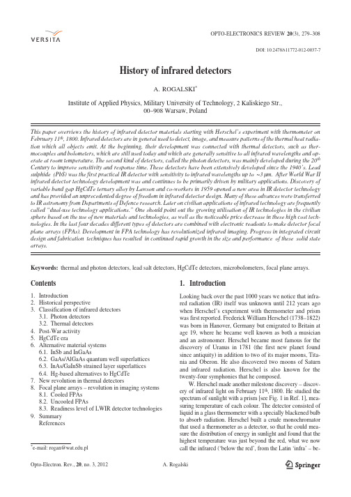
History of infrared detectorsA.ROGALSKI*Institute of Applied Physics, Military University of Technology, 2 Kaliskiego Str.,00–908 Warsaw, PolandThis paper overviews the history of infrared detector materials starting with Herschel’s experiment with thermometer on February11th,1800.Infrared detectors are in general used to detect,image,and measure patterns of the thermal heat radia−tion which all objects emit.At the beginning,their development was connected with thermal detectors,such as ther−mocouples and bolometers,which are still used today and which are generally sensitive to all infrared wavelengths and op−erate at room temperature.The second kind of detectors,called the photon detectors,was mainly developed during the20th Century to improve sensitivity and response time.These detectors have been extensively developed since the1940’s.Lead sulphide(PbS)was the first practical IR detector with sensitivity to infrared wavelengths up to~3μm.After World War II infrared detector technology development was and continues to be primarily driven by military applications.Discovery of variable band gap HgCdTe ternary alloy by Lawson and co−workers in1959opened a new area in IR detector technology and has provided an unprecedented degree of freedom in infrared detector design.Many of these advances were transferred to IR astronomy from Departments of Defence ter on civilian applications of infrared technology are frequently called“dual−use technology applications.”One should point out the growing utilisation of IR technologies in the civilian sphere based on the use of new materials and technologies,as well as the noticeable price decrease in these high cost tech−nologies.In the last four decades different types of detectors are combined with electronic readouts to make detector focal plane arrays(FPAs).Development in FPA technology has revolutionized infrared imaging.Progress in integrated circuit design and fabrication techniques has resulted in continued rapid growth in the size and performance of these solid state arrays.Keywords:thermal and photon detectors, lead salt detectors, HgCdTe detectors, microbolometers, focal plane arrays.Contents1.Introduction2.Historical perspective3.Classification of infrared detectors3.1.Photon detectors3.2.Thermal detectors4.Post−War activity5.HgCdTe era6.Alternative material systems6.1.InSb and InGaAs6.2.GaAs/AlGaAs quantum well superlattices6.3.InAs/GaInSb strained layer superlattices6.4.Hg−based alternatives to HgCdTe7.New revolution in thermal detectors8.Focal plane arrays – revolution in imaging systems8.1.Cooled FPAs8.2.Uncooled FPAs8.3.Readiness level of LWIR detector technologies9.SummaryReferences 1.IntroductionLooking back over the past1000years we notice that infra−red radiation(IR)itself was unknown until212years ago when Herschel’s experiment with thermometer and prism was first reported.Frederick William Herschel(1738–1822) was born in Hanover,Germany but emigrated to Britain at age19,where he became well known as both a musician and an astronomer.Herschel became most famous for the discovery of Uranus in1781(the first new planet found since antiquity)in addition to two of its major moons,Tita−nia and Oberon.He also discovered two moons of Saturn and infrared radiation.Herschel is also known for the twenty−four symphonies that he composed.W.Herschel made another milestone discovery–discov−ery of infrared light on February11th,1800.He studied the spectrum of sunlight with a prism[see Fig.1in Ref.1],mea−suring temperature of each colour.The detector consisted of liquid in a glass thermometer with a specially blackened bulb to absorb radiation.Herschel built a crude monochromator that used a thermometer as a detector,so that he could mea−sure the distribution of energy in sunlight and found that the highest temperature was just beyond the red,what we now call the infrared(‘below the red’,from the Latin‘infra’–be−OPTO−ELECTRONICS REVIEW20(3),279–308DOI: 10.2478/s11772−012−0037−7*e−mail: rogan@.pllow)–see Fig.1(b)[2].In April 1800he reported it to the Royal Society as dark heat (Ref.1,pp.288–290):Here the thermometer No.1rose 7degrees,in 10minu−tes,by an exposure to the full red coloured rays.I drew back the stand,till the centre of the ball of No.1was just at the vanishing of the red colour,so that half its ball was within,and half without,the visible rays of theAnd here the thermometerin 16minutes,degrees,when its centre was inch out of the raysof the sun.as had a rising of 9de−grees,and here the difference is almost too trifling to suppose,that latter situation of the thermometer was much beyond the maximum of the heating power;while,at the same time,the experiment sufficiently indi−cates,that the place inquired after need not be looked for at a greater distance.Making further experiments on what Herschel called the ‘calorific rays’that existed beyond the red part of the spec−trum,he found that they were reflected,refracted,absorbed and transmitted just like visible light [1,3,4].The early history of IR was reviewed about 50years ago in three well−known monographs [5–7].Many historical information can be also found in four papers published by Barr [3,4,8,9]and in more recently published monograph [10].Table 1summarises the historical development of infrared physics and technology [11,12].2.Historical perspectiveFor thirty years following Herschel’s discovery,very little progress was made beyond establishing that the infrared ra−diation obeyed the simplest laws of optics.Slow progress inthe study of infrared was caused by the lack of sensitive and accurate detectors –the experimenters were handicapped by the ordinary thermometer.However,towards the second de−cade of the 19th century,Thomas Johann Seebeck began to examine the junction behaviour of electrically conductive materials.In 1821he discovered that a small electric current will flow in a closed circuit of two dissimilar metallic con−ductors,when their junctions are kept at different tempera−tures [13].During that time,most physicists thought that ra−diant heat and light were different phenomena,and the dis−covery of Seebeck indirectly contributed to a revival of the debate on the nature of heat.Due to small output vol−tage of Seebeck’s junctions,some μV/K,the measurement of very small temperature differences were prevented.In 1829L.Nobili made the first thermocouple and improved electrical thermometer based on the thermoelectric effect discovered by Seebeck in 1826.Four years later,M.Melloni introduced the idea of connecting several bismuth−copper thermocouples in series,generating a higher and,therefore,measurable output voltage.It was at least 40times more sensitive than the best thermometer available and could de−tect the heat from a person at a distance of 30ft [8].The out−put voltage of such a thermopile structure linearly increases with the number of connected thermocouples.An example of thermopile’s prototype invented by Nobili is shown in Fig.2(a).It consists of twelve large bismuth and antimony elements.The elements were placed upright in a brass ring secured to an adjustable support,and were screened by a wooden disk with a 15−mm central aperture.Incomplete version of the Nobili−Melloni thermopile originally fitted with the brass cone−shaped tubes to collect ra−diant heat is shown in Fig.2(b).This instrument was much more sensi−tive than the thermometers previously used and became the most widely used detector of IR radiation for the next half century.The third member of the trio,Langley’s bolometer appea−red in 1880[7].Samuel Pierpont Langley (1834–1906)used two thin ribbons of platinum foil connected so as to form two arms of a Wheatstone bridge (see Fig.3)[15].This instrument enabled him to study solar irradiance far into its infrared region and to measure theintensityof solar radia−tion at various wavelengths [9,16,17].The bolometer’s sen−History of infrared detectorsFig.1.Herschel’s first experiment:A,B –the small stand,1,2,3–the thermometers upon it,C,D –the prism at the window,E –the spec−trum thrown upon the table,so as to bring the last quarter of an inch of the read colour upon the stand (after Ref.1).InsideSir FrederickWilliam Herschel (1738–1822)measures infrared light from the sun– artist’s impression (after Ref. 2).Fig.2.The Nobili−Meloni thermopiles:(a)thermopile’s prototype invented by Nobili (ca.1829),(b)incomplete version of the Nobili−−Melloni thermopile (ca.1831).Museo Galileo –Institute and Museum of the History of Science,Piazza dei Giudici 1,50122Florence, Italy (after Ref. 14).Table 1. Milestones in the development of infrared physics and technology (up−dated after Refs. 11 and 12)Year Event1800Discovery of the existence of thermal radiation in the invisible beyond the red by W. HERSCHEL1821Discovery of the thermoelectric effects using an antimony−copper pair by T.J. SEEBECK1830Thermal element for thermal radiation measurement by L. NOBILI1833Thermopile consisting of 10 in−line Sb−Bi thermal pairs by L. NOBILI and M. MELLONI1834Discovery of the PELTIER effect on a current−fed pair of two different conductors by J.C. PELTIER1835Formulation of the hypothesis that light and electromagnetic radiation are of the same nature by A.M. AMPERE1839Solar absorption spectrum of the atmosphere and the role of water vapour by M. MELLONI1840Discovery of the three atmospheric windows by J. HERSCHEL (son of W. HERSCHEL)1857Harmonization of the three thermoelectric effects (SEEBECK, PELTIER, THOMSON) by W. THOMSON (Lord KELVIN)1859Relationship between absorption and emission by G. KIRCHHOFF1864Theory of electromagnetic radiation by J.C. MAXWELL1873Discovery of photoconductive effect in selenium by W. SMITH1876Discovery of photovoltaic effect in selenium (photopiles) by W.G. ADAMS and A.E. DAY1879Empirical relationship between radiation intensity and temperature of a blackbody by J. STEFAN1880Study of absorption characteristics of the atmosphere through a Pt bolometer resistance by S.P. LANGLEY1883Study of transmission characteristics of IR−transparent materials by M. MELLONI1884Thermodynamic derivation of the STEFAN law by L. BOLTZMANN1887Observation of photoelectric effect in the ultraviolet by H. HERTZ1890J. ELSTER and H. GEITEL constructed a photoemissive detector consisted of an alkali−metal cathode1894, 1900Derivation of the wavelength relation of blackbody radiation by J.W. RAYEIGH and W. WIEN1900Discovery of quantum properties of light by M. PLANCK1903Temperature measurements of stars and planets using IR radiometry and spectrometry by W.W. COBLENTZ1905 A. EINSTEIN established the theory of photoelectricity1911R. ROSLING made the first television image tube on the principle of cathode ray tubes constructed by F. Braun in 18971914Application of bolometers for the remote exploration of people and aircrafts ( a man at 200 m and a plane at 1000 m)1917T.W. CASE developed the first infrared photoconductor from substance composed of thallium and sulphur1923W. SCHOTTKY established the theory of dry rectifiers1925V.K. ZWORYKIN made a television image tube (kinescope) then between 1925 and 1933, the first electronic camera with the aid of converter tube (iconoscope)1928Proposal of the idea of the electro−optical converter (including the multistage one) by G. HOLST, J.H. DE BOER, M.C. TEVES, and C.F. VEENEMANS1929L.R. KOHLER made a converter tube with a photocathode (Ag/O/Cs) sensitive in the near infrared1930IR direction finders based on PbS quantum detectors in the wavelength range 1.5–3.0 μm for military applications (GUDDEN, GÖRLICH and KUTSCHER), increased range in World War II to 30 km for ships and 7 km for tanks (3–5 μm)1934First IR image converter1939Development of the first IR display unit in the United States (Sniperscope, Snooperscope)1941R.S. OHL observed the photovoltaic effect shown by a p−n junction in a silicon1942G. EASTMAN (Kodak) offered the first film sensitive to the infrared1947Pneumatically acting, high−detectivity radiation detector by M.J.E. GOLAY1954First imaging cameras based on thermopiles (exposure time of 20 min per image) and on bolometers (4 min)1955Mass production start of IR seeker heads for IR guided rockets in the US (PbS and PbTe detectors, later InSb detectors for Sidewinder rockets)1957Discovery of HgCdTe ternary alloy as infrared detector material by W.D. LAWSON, S. NELSON, and A.S. YOUNG1961Discovery of extrinsic Ge:Hg and its application (linear array) in the first LWIR FLIR systems1965Mass production start of IR cameras for civil applications in Sweden (single−element sensors with optomechanical scanner: AGA Thermografiesystem 660)1970Discovery of charge−couple device (CCD) by W.S. BOYLE and G.E. SMITH1970Production start of IR sensor arrays (monolithic Si−arrays: R.A. SOREF 1968; IR−CCD: 1970; SCHOTTKY diode arrays: F.D.SHEPHERD and A.C. YANG 1973; IR−CMOS: 1980; SPRITE: T. ELIOTT 1981)1975Lunch of national programmes for making spatially high resolution observation systems in the infrared from multielement detectors integrated in a mini cooler (so−called first generation systems): common module (CM) in the United States, thermal imaging commonmodule (TICM) in Great Britain, syteme modulaire termique (SMT) in France1975First In bump hybrid infrared focal plane array1977Discovery of the broken−gap type−II InAs/GaSb superlattices by G.A. SAI−HALASZ, R. TSU, and L. ESAKI1980Development and production of second generation systems [cameras fitted with hybrid HgCdTe(InSb)/Si(readout) FPAs].First demonstration of two−colour back−to−back SWIR GaInAsP detector by J.C. CAMPBELL, A.G. DENTAI, T.P. LEE,and C.A. BURRUS1985Development and mass production of cameras fitted with Schottky diode FPAs (platinum silicide)1990Development and production of quantum well infrared photoconductor (QWIP) hybrid second generation systems1995Production start of IR cameras with uncooled FPAs (focal plane arrays; microbolometer−based and pyroelectric)2000Development and production of third generation infrared systemssitivity was much greater than that of contemporary thermo−piles which were little improved since their use by Melloni. Langley continued to develop his bolometer for the next20 years(400times more sensitive than his first efforts).His latest bolometer could detect the heat from a cow at a dis−tance of quarter of mile [9].From the above information results that at the beginning the development of the IR detectors was connected with ther−mal detectors.The first photon effect,photoconductive ef−fect,was discovered by Smith in1873when he experimented with selenium as an insulator for submarine cables[18].This discovery provided a fertile field of investigation for several decades,though most of the efforts were of doubtful quality. By1927,over1500articles and100patents were listed on photosensitive selenium[19].It should be mentioned that the literature of the early1900’s shows increasing interest in the application of infrared as solution to numerous problems[7].A special contribution of William Coblenz(1873–1962)to infrared radiometry and spectroscopy is marked by huge bib−liography containing hundreds of scientific publications, talks,and abstracts to his credit[20,21].In1915,W.Cob−lentz at the US National Bureau of Standards develops ther−mopile detectors,which he uses to measure the infrared radi−ation from110stars.However,the low sensitivity of early in−frared instruments prevented the detection of other near−IR sources.Work in infrared astronomy remained at a low level until breakthroughs in the development of new,sensitive infrared detectors were achieved in the late1950’s.The principle of photoemission was first demonstrated in1887when Hertz discovered that negatively charged par−ticles were emitted from a conductor if it was irradiated with ultraviolet[22].Further studies revealed that this effect could be produced with visible radiation using an alkali metal electrode [23].Rectifying properties of semiconductor−metal contact were discovered by Ferdinand Braun in1874[24],when he probed a naturally−occurring lead sulphide(galena)crystal with the point of a thin metal wire and noted that current flowed freely in one direction only.Next,Jagadis Chandra Bose demonstrated the use of galena−metal point contact to detect millimetre electromagnetic waves.In1901he filed a U.S patent for a point−contact semiconductor rectifier for detecting radio signals[25].This type of contact called cat’s whisker detector(sometimes also as crystal detector)played serious role in the initial phase of radio development.How−ever,this contact was not used in a radiation detector for the next several decades.Although crystal rectifiers allowed to fabricate simple radio sets,however,by the mid−1920s the predictable performance of vacuum−tubes replaced them in most radio applications.The period between World Wars I and II is marked by the development of photon detectors and image converters and by emergence of infrared spectroscopy as one of the key analytical techniques available to chemists.The image con−verter,developed on the eve of World War II,was of tre−mendous interest to the military because it enabled man to see in the dark.The first IR photoconductor was developed by Theodore W.Case in1917[26].He discovered that a substance com−posed of thallium and sulphur(Tl2S)exhibited photocon−ductivity.Supported by the US Army between1917and 1918,Case adapted these relatively unreliable detectors for use as sensors in an infrared signalling device[27].The pro−totype signalling system,consisting of a60−inch diameter searchlight as the source of radiation and a thallous sulphide detector at the focus of a24−inch diameter paraboloid mir−ror,sent messages18miles through what was described as ‘smoky atmosphere’in1917.However,instability of resis−tance in the presence of light or polarizing voltage,loss of responsivity due to over−exposure to light,high noise,slug−gish response and lack of reproducibility seemed to be inhe−rent weaknesses.Work was discontinued in1918;commu−nication by the detection of infrared radiation appeared dis−tinctly ter Case found that the addition of oxygen greatly enhanced the response [28].The idea of the electro−optical converter,including the multistage one,was proposed by Holst et al.in1928[29]. The first attempt to make the converter was not successful.A working tube consisted of a photocathode in close proxi−mity to a fluorescent screen was made by the authors in 1934 in Philips firm.In about1930,the appearance of the Cs−O−Ag photo−tube,with stable characteristics,to great extent discouraged further development of photoconductive cells until about 1940.The Cs−O−Ag photocathode(also called S−1)elabo−History of infrared detectorsFig.3.Longley’s bolometer(a)composed of two sets of thin plati−num strips(b),a Wheatstone bridge,a battery,and a galvanometer measuring electrical current (after Ref. 15 and 16).rated by Koller and Campbell[30]had a quantum efficiency two orders of magnitude above anything previously studied, and consequently a new era in photoemissive devices was inaugurated[31].In the same year,the Japanese scientists S. Asao and M.Suzuki reported a method for enhancing the sensitivity of silver in the S−1photocathode[32].Consisted of a layer of caesium on oxidized silver,S−1is sensitive with useful response in the near infrared,out to approxi−mately1.2μm,and the visible and ultraviolet region,down to0.3μm.Probably the most significant IR development in the United States during1930’s was the Radio Corporation of America(RCA)IR image tube.During World War II, near−IR(NIR)cathodes were coupled to visible phosphors to provide a NIR image converter.With the establishment of the National Defence Research Committee,the develop−ment of this tube was accelerated.In1942,the tube went into production as the RCA1P25image converter(see Fig.4).This was one of the tubes used during World War II as a part of the”Snooperscope”and”Sniperscope,”which were used for night observation with infrared sources of illumination.Since then various photocathodes have been developed including bialkali photocathodes for the visible region,multialkali photocathodes with high sensitivity ex−tending to the infrared region and alkali halide photocatho−des intended for ultraviolet detection.The early concepts of image intensification were not basically different from those today.However,the early devices suffered from two major deficiencies:poor photo−cathodes and poor ter development of both cathode and coupling technologies changed the image in−tensifier into much more useful device.The concept of image intensification by cascading stages was suggested independently by number of workers.In Great Britain,the work was directed toward proximity focused tubes,while in the United State and in Germany–to electrostatically focused tubes.A history of night vision imaging devices is given by Biberman and Sendall in monograph Electro−Opti−cal Imaging:System Performance and Modelling,SPIE Press,2000[10].The Biberman’s monograph describes the basic trends of infrared optoelectronics development in the USA,Great Britain,France,and Germany.Seven years later Ponomarenko and Filachev completed this monograph writ−ing the book Infrared Techniques and Electro−Optics in Russia:A History1946−2006,SPIE Press,about achieve−ments of IR techniques and electrooptics in the former USSR and Russia [33].In the early1930’s,interest in improved detectors began in Germany[27,34,35].In1933,Edgar W.Kutzscher at the University of Berlin,discovered that lead sulphide(from natural galena found in Sardinia)was photoconductive and had response to about3μm.B.Gudden at the University of Prague used evaporation techniques to develop sensitive PbS films.Work directed by Kutzscher,initially at the Uni−versity of Berlin and later at the Electroacustic Company in Kiel,dealt primarily with the chemical deposition approach to film formation.This work ultimately lead to the fabrica−tion of the most sensitive German detectors.These works were,of course,done under great secrecy and the results were not generally known until after1945.Lead sulphide photoconductors were brought to the manufacturing stage of development in Germany in about1943.Lead sulphide was the first practical infrared detector deployed in a variety of applications during the war.The most notable was the Kiel IV,an airborne IR system that had excellent range and which was produced at Carl Zeiss in Jena under the direction of Werner K. Weihe [6].In1941,Robert J.Cashman improved the technology of thallous sulphide detectors,which led to successful produc−tion[36,37].Cashman,after success with thallous sulphide detectors,concentrated his efforts on lead sulphide detec−tors,which were first produced in the United States at Northwestern University in1944.After World War II Cash−man found that other semiconductors of the lead salt family (PbSe and PbTe)showed promise as infrared detectors[38]. The early detector cells manufactured by Cashman are shown in Fig. 5.Fig.4.The original1P25image converter tube developed by the RCA(a).This device measures115×38mm overall and has7pins.It opera−tion is indicated by the schematic drawing (b).After1945,the wide−ranging German trajectory of research was essentially the direction continued in the USA, Great Britain and Soviet Union under military sponsorship after the war[27,39].Kutzscher’s facilities were captured by the Russians,thus providing the basis for early Soviet detector development.From1946,detector technology was rapidly disseminated to firms such as Mullard Ltd.in Southampton,UK,as part of war reparations,and some−times was accompanied by the valuable tacit knowledge of technical experts.E.W.Kutzscher,for example,was flown to Britain from Kiel after the war,and subsequently had an important influence on American developments when he joined Lockheed Aircraft Co.in Burbank,California as a research scientist.Although the fabrication methods developed for lead salt photoconductors was usually not completely under−stood,their properties are well established and reproducibi−lity could only be achieved after following well−tried reci−pes.Unlike most other semiconductor IR detectors,lead salt photoconductive materials are used in the form of polycrys−talline films approximately1μm thick and with individual crystallites ranging in size from approximately0.1–1.0μm. They are usually prepared by chemical deposition using empirical recipes,which generally yields better uniformity of response and more stable results than the evaporative methods.In order to obtain high−performance detectors, lead chalcogenide films need to be sensitized by oxidation. The oxidation may be carried out by using additives in the deposition bath,by post−deposition heat treatment in the presence of oxygen,or by chemical oxidation of the film. The effect of the oxidant is to introduce sensitizing centres and additional states into the bandgap and thereby increase the lifetime of the photoexcited holes in the p−type material.3.Classification of infrared detectorsObserving a history of the development of the IR detector technology after World War II,many materials have been investigated.A simple theorem,after Norton[40],can be stated:”All physical phenomena in the range of about0.1–1 eV will be proposed for IR detectors”.Among these effects are:thermoelectric power(thermocouples),change in elec−trical conductivity(bolometers),gas expansion(Golay cell), pyroelectricity(pyroelectric detectors),photon drag,Jose−phson effect(Josephson junctions,SQUIDs),internal emis−sion(PtSi Schottky barriers),fundamental absorption(in−trinsic photodetectors),impurity absorption(extrinsic pho−todetectors),low dimensional solids[superlattice(SL), quantum well(QW)and quantum dot(QD)detectors], different type of phase transitions, etc.Figure6gives approximate dates of significant develop−ment efforts for the materials mentioned.The years during World War II saw the origins of modern IR detector tech−nology.Recent success in applying infrared technology to remote sensing problems has been made possible by the successful development of high−performance infrared de−tectors over the last six decades.Photon IR technology com−bined with semiconductor material science,photolithogra−phy technology developed for integrated circuits,and the impetus of Cold War military preparedness have propelled extraordinary advances in IR capabilities within a short time period during the last century [41].The majority of optical detectors can be classified in two broad categories:photon detectors(also called quantum detectors) and thermal detectors.3.1.Photon detectorsIn photon detectors the radiation is absorbed within the material by interaction with electrons either bound to lattice atoms or to impurity atoms or with free electrons.The observed electrical output signal results from the changed electronic energy distribution.The photon detectors show a selective wavelength dependence of response per unit incident radiation power(see Fig.8).They exhibit both a good signal−to−noise performance and a very fast res−ponse.But to achieve this,the photon IR detectors require cryogenic cooling.This is necessary to prevent the thermalHistory of infrared detectorsFig.5.Cashman’s detector cells:(a)Tl2S cell(ca.1943):a grid of two intermeshing comb−line sets of conducting paths were first pro−vided and next the T2S was evaporated over the grid structure;(b) PbS cell(ca.1945)the PbS layer was evaporated on the wall of the tube on which electrical leads had been drawn with aquadag(afterRef. 38).。
乱花渐欲迷人眼 2007秋季DC新品特辑
乱花渐欲迷人眼 2007秋季DC新品特辑
佚名
【期刊名称】《数码》
【年(卷),期】2007(000)010
【摘要】2007年秋,注定是个DSLR混战,影友狂欢的时刻,除了老牌影像厂商佳能、尼康隆重推出各自的中、高端数码单反新品,博得影友无数眼球外,刚刚进入DSLR市场1年有余的新兴势力索尼也不遗余力,携中端数码单反产品α700
汹涌而来。
便携型消费级数码相机方面,索尼、佳能、尼康、奥林巴斯、柯达等DC厂商也都积极展开了新一轮的产品升级攻势。
一时之间,竟恍如身入百花丛中,颇有乱花渐欲这人眼之感。
如此这般,就让小编为大家理理脉络,看看究竟有哪些产品问世,哪些精品值得我们关注吧!
【总页数】6页(P98-103)
【正文语种】中文
【中图分类】TB852.1
【相关文献】
1.testo 327全新锅炉燃烧效率分析仪亮相德图2007年秋季新品发布 [J],
2.乱花渐欲迷人眼——Broadcast Asia 2007展会报道 [J], 马海龙
3.新加坡,HP,以娱乐的方式——2007HP全球战略暨秋季新品发布会 [J],
4.2007通信展新品特辑 [J],
5.为人生添彩,助商务腾飞——2007年佳能(中国)秋季打印机新品发布会在京召开 [J],
因版权原因,仅展示原文概要,查看原文内容请购买。
电源也玩半导体散热多彩ICE CUBE-550极冻电源
电源也玩半导体散热多彩ICE CUBE-550极冻电源
佚名
【期刊名称】《《微型计算机》》
【年(卷),期】2006(000)024
【摘要】最近多彩新推出了一款极冻电源,定位于多彩精品系列.额定功率达到了550W,双路+12V输出可以分别达到17A.并具备过压、欠压、过功率、过温度、短路等多重保护功能。
和其它电源不同的是,多彩极冻电源采用了一块半导体制冷片.是国内首款采用半导体制冷片进行散热的电源产品。
【总页数】1页(P14)
【正文语种】中文
【相关文献】
1.智能散热有一套——多彩320A电源简介 [J],
2.电源也玩半导体散热——多彩ICE CUBE-550极冻电源 [J], 雷军
3.香港理工大学获安森美半导体赞助勇夺国际电源设计挑战赛大奖:得奖作品采用安森美半导体节能开关电源模式电源控制芯片 [J],
4.用做板卡的精神做电源、散热器华硕电脑电源、散热器部门高层专访摘要 [J], MC[1];杨承翰[1];吴卓刚[1];陈列[1]
5.599元的550W电源极冻酷凌冰川GP-PS550BP电源 [J],
因版权原因,仅展示原文概要,查看原文内容请购买。
英伟达超算中心浸没式冷却液方案
英伟达超算中心浸没式冷却液方案一、引言随着科技的进步,超级计算机已经成为许多科学领域研究、工程模拟和数据处理的基础工具。
然而,随着计算机性能的提高,散热问题也变得愈发突出。
因此,设计一套高效可靠的冷却液方案变得至关重要。
本文将采用英伟达超算中心作为实际案例,详细介绍一种浸没式冷却液方案。
二、方案设计1.冷却液的选择冷却液是浸没式冷却系统的核心。
为了保证高效的散热效果,我们推荐选用液态冷却剂。
液态冷却剂的热导率较高,并且具有良好的散热性能。
同时,冷却液还需具备良好的绝缘性能,以保证设备的运行安全。
我们推荐选用高纯度无水醇类冷却液作为基础液体,并根据实际需求加入合适的添加剂,如界面活性剂和抗菌剂。
2.浸没式冷却系统的设计为了实现浸没式冷却效果,需在超级计算机的整个设备上方设计一层浸没式冷却池。
冷却池的材质应选用具有良好耐腐蚀性和绝缘性的材料,如陶瓷。
冷却池应具备良好的密封性能,确保冷却液不会泄漏。
在冷却池底部,设计一套循环冷却系统,将冷却池中的液体通过冷却装置循环使用,保持流动的冷却液始终保持较低的温度,从而实现设备的散热效果。
3.传感器与控制系统在浸没式冷却液方案中,传感器和控制系统是非常重要的一部分。
通过在冷却池中布置温度传感器,可以实时监测冷却液的温度情况,并将数据反馈给控制系统。
控制系统将根据温度情况,自动调节冷却液的循环速度和冷却设备的功率,使冷却液的温度保持在合适范围内。
同时,控制系统还需要具备报警功能,当冷却液温度异常时,及时发出警报,以避免过高温度对设备的损坏。
4.安全与环保考虑在浸没式冷却液方案中,安全性和环保性是非常重要的考虑因素。
首先,冷却液的选用应遵循环保原则,选择无毒、无害的冷却液。
其次,在冷却池和循环系统中,需设置过滤装置,保证冷却液中不会存在杂质和颗粒,以避免对设备的损害。
此外,在冷却系统中还需设置流量监测装置,当冷却液流动异常时,及时报警并停止运行,以避免进一步的损害。
Allied Precision Industries, Inc. 冰膜电泵模型7521、7621、
3. Some animals--particularily horses--may try to remove the deicer from the tank. To counteract this, you may wish to run the cord through PVC or galvanized tubing extending over the tank or use the API Deicer Safety Tether Model 23ST. Be sure to allow slack in the cord to compensate for varying water level.
- To test the unit: Place the de-icer in a freezer for 20 minutes to make sure that the thermostat is turned on. Locate a GFCI outlet (typically found in a bathroom in newer homes) and run some water into a bucket, sink, or bathtub near the outlet. Quickly remove the unit from the freezer, place it into the water, and plug the unit into the GFCI while taking care not to touch the water. If the unit trips the GFCI, it is defective and should be returned to the place of purchase. If it does not trip the GFCI, it is operating properly and is not leaking electricity to the water. However, there could be electricity entering the tank via the ground wire due to presence of voltage on the ground circuit in the electrical supply from the building. Many times, this voltage is coming directly from the electric utility company. For help with this problem, contact Allied Precision at (800) 627-6179 or (630) 365-0340.