Adaptive Checkpointing with Storage Management for Mobile Environments
nrf5 SDK 中文翻译(五)——寻向功能篇

[公司名称]nRF5 SDK 中文翻译——寻向功能篇[作者姓名]2022-4-29修订历史目录..目录 (1)第1章驱动支持列表..............................................................................错误!未定义书签。
第2章Clock 时钟 ..................................................................................错误!未定义书签。
2.1 简介.............................................................................................错误!未定义书签。
2.2 驱动配置.....................................................................................错误!未定义书签。
2.3 控制HFCLK...............................................................................错误!未定义书签。
2.4 控制LFCLK(仅在不带SoftDevice的情况下) ...................错误!未定义书签。
2.5 控制LFCLK的校准(不带软设备并使用RC作为时钟源) .......错误!未定义书签。
第3章COMP (比较器)...........................................................................错误!未定义书签。
3.1 简介.............................................................................................错误!未定义书签。
adaptec Adaptec 6系列和5Z系列 RAID控制卡的零维护缓存保护

零维护缓存保护简报降低数据中心运营成本,最大限度保护缓存数据产品要点低运营成本– 没有电池相关的安装、监控、维护、弃置或者更换成本停电情况下不会丢失数据– 取代锂电池零维护缓存保护– 无需监测电池充电情况– 更换电池过程中不需要关闭系统– 无限期地保护数据 -“在电池电量耗尽之前”不需要急于重启系统– 保存数据长达数年之久RAID缓存即时保护– 充电只需要几分钟时间,而不是几小时– 环境优化RAID性能环保– 无毒电池废弃处理– 配合Adaptec智能电源管理功能打造行业“最绿色”解决方案- 遵从简化的 IATA 规则完全集成在5Z系列RAID控制上并作为6系列的附件套件IDC预计,在四年时间内一步IT设备的运营成本将增长到原始采购成本的4倍。
Adaptec 6系列和5Z系列RAID控制卡采用了零维护缓存保护(Zero-Maintenance CacheProtection,ZMCP)功能,最大限度保护缓存数据,大幅削减成本并减少了复杂、杂乱和昂贵的锂电池对环境的影响,同时提高了缓存保护和缓存性能。
为什么你需要缓存保护随着用户持续关注针对快速增加的数据集进行的容量利用率优化,RAID 5和RAID 6在企业级存储系统中的运用继续增长着。
然而,除非启用了所有可用缓存,否则系统无法实现最佳性能。
不过,启用控制卡缓存之后,数据被保存在控制卡的内存中,并有可能在系统断电的情况下丢失。
防止这种情况发生的最常见保护措施就是使用一个直接安装在控制卡上的电池备份单元(BBU)来备份控制卡缓存。
这种电池是维护板载缓存数据,直到恢复对电池备份单元的供电。
电池备份单元的第二个使用方法就是配合Adaptec 6系列、5Z系列、5系列和2系列RAID控制卡产品系列所提供的Adaptec智能电源管理功能(Intelligent Power Management)。
为了让控制卡降低硬盘转速或者完全停转,硬盘中必须是没有任何I/O活动的。
微芯片Adaptec产品指南:信任存储解决方案说明书

Adaptec ® Product GuideTrusted Storage SolutionsData Center SolutionsThe Microchip name and logo, the Microchip logo, Adaptec and maxCrypto is a trademark are registered trademarks of Microchip Technology Incorporated in the U.S.A. and other countries. All other trademarks mentioned herein are property of their respective companies.© 2020, Microchip Technology Incorporated. All Rights Reserved. 1/20 DS00003375ASupportMicrochip is committed to supporting its customers in developing products faster and more efficiently. We maintain a worldwide network of field applica -tions engineers and technical support ready to provide product and system assistance. For more information, please visit :• Technical Support: /support • Evaluation samples of any Microchip device:/sample • Knowledge base and peer help:/forums• Sales and Global Distribution: /salesTrainingIf additional training interests you, Microchip offers several resources including in-depth technical training and reference material, self-paced tutorials and significant online resources.• Overview of Technical Training Resources: /training • MASTERs Conferences:/masters • Developer Help Website:/developerhelp • Technical Training Centers:/seminarsMicrochip Technology Inc. | 2355 W. Chandler Blvd. | Chandler AZ, 85224-6199Adaptec ® Product GuideEach New Product Family Has Unique, Differentiating FeaturesSmartRAID 3100The SmartRAID 3100 is optimized for Enterprise storage applications that require the highest level of data availability and data center applications that benefit from caching.• Adapters with up to 24 ports using 28 nm SAS/SATA-optimized silicon, offering the industry’s lowest power • Z ero Maintenance Cache Protection (ZMCP) with a cache size up to 4 GB with integrated cache backupcircuitry for optimal cost, thermal performance and operating efficiency • Board options without cache backup• Mixed mode enables drives to be independently configured as raw drives or as part of a logical volume • maxCache 4.0 included on 315x and 316x adapters• maxCrypto controller-based encryption on the 3162-8i/e adapterSmartHBA 2100The SmartHBA 2100 is optimized for Software-Defined Storage (SDS) applications that require hardware RAID for OS boot drives as well as entry-level RAID for SMBs.• The only basic hardware RAID solution offering a fully featured, high-performance Host Bus Adapter(HBA) for drives configured as raw drives, required for multi-path IO and SDS applications • RAID levels 0, 1, 10, 5• Industry’s only basic hardware RAID solution with more than 8 ports• Mixed mode enables drives to be independently configured as raw drives or as part of a logical volumeHBA 1100The HBA 1100 is optimized for SDS, cold storage, and raw high-performance connectivity.• Adapters with up to 24 ports using 28 nm SAS/SATA-optimized silicon, offering the industry’s lowestpower• Support for host-managed and host-aware Shingled Magnetic Recording (SMR) drives • Broad OS driver support, including inbox driver support • Performance of up to 1.7M IOPS Smart Storage Solutions OverviewCablesSmartRAIDSmartRAIDSmartHBASmartRAID 3100 RAID AdaptersAdaptec 12 Gbps SmartRAID 3100 adapters have an 8-lane PCIe ®Gen 3 host bus interface, a SmartROC 3100 processor, an MD2 low-profile form factor, and can be scaled to a maximum of 256 SAS/SATA devices*. The newest addition, the SmartRAID 3162-8i/e, provides the industry’s only data-at-rest controller-based encryption solution, maxCrypto. Supporting operating systems include include Microsoft Windows ®, Red Hat, SUSE, Fedora, Debian, Ubuntu, Sun Solaris, FreeBSD, VMware ESXi, open-source Linux ®drivers and inbox drivers.Series 8 RAID AdaptersAdaptec 12 Gbps RAID Adapters have an 8-lane PCIe Gen3 host bus interface,a 12 Gbps RoC processor, a MD2 low-profile form factor, and can be scaled to a maximum of 256 SAS/SATA devices*. Supporting operating systems include Microsoft Windows, Red Hat Linux, SUSE Linux, Fedora, Debian Linux, Ubuntu Linux,Sun Solaris, FreeBSD and VMware ESXi.SmartHBA and Host Bus Adapters (HBA)Adaptec 12 Gbps HBAs have an 8-lane PCIe Gen 3 host bus interface, a SmartIOC 2100 processor, an MD2 low-profile form factor, and can be scaled to a max -imum of 256 SAS/SATA devices*. In addition, the SmartHBA 2100 series uniquely combines the capabilities of a full-featured HBA, with those of a basic hardware RAID adapter. Supporting operating systems include Microsoft Windows, Red Hat, SuSE, CentOS, Ubuntu, VMware ESXi, FreeBSD, Solaris and Citrix Xen Server.SmartHBA 2100 Host Bus Adaptor Specifications4SAS-SBExternal CablesACK-E-HDmSAS-HDmSASACK-E-HDmSAS-mSASMake the Right Connection With Adaptec 12 Gbps and 6 Gbps SAS HD CablesAdaptec SmartRAID 3100, SmartHBA 2100, HBA 1100 and Series 8/8Q/8E RAID adapters are configured with mini-SAS HD connectors to allow for maximum performance and connectivity in a MD2 low-profile form factor. Pick the right cable for your internal or external storage solution.。
Entrust Adaptive Issuance Instant ID软件产品介绍说明书

Entrust Adaptive Issuance Instant ID SoftwareHIGHLIGHTSLaunch your ID card program with confidenceEntrust Adaptive Issuance Instant ID software is the ideal starting point for organizations that want to make their people and premises more secure. Built for a single-user environment, InstantID software delivers the core tools you need to easily design, print, and manage ID cards and credentials. This user-friendly software offers you a complete solution for issuing basic IDs. Plus, you can easily scale up to another, more feature-rich edition in the Instant ID software suite as your needs grow.KEY BENEFITSEase of use. Drag-and-drop features make the software intuitive and easyto use, allowing you to spend less time learning and more time creating new credentials.• B rowser-based applications do notrequire an internet connection.• P rovides administrators with anintuitive interface to build the rightworkflows and card design. Everyday users can automatically follow astandardized process to improveaccuracy.• T he Quick Start Wizard gets usersfrom initial login to print with minimal setup and configuration.Configure to meet your needs. Settings can be configured to allow everyday users the ability to capture the data they want, how they want, while ensuring only the proper information is captured. Use your existing data. Import data from CSV and ASCII files or integrate directly with Microsoft Access, SQL Server, or MySQL*.*Available with Instant ID Plus editionEntrust Adaptive Issuance at a glanceEntrust Adaptive Issuance Instant ID offers a basic card issuance edition that’s just right for you – now and into the future.Instant ID Express software includes:• B asic photo capture• Data import• Credential designer• D rag-and-drop workflowsfor a single-user environment• E mbedded database for record storage and retrieval Instant ID Plus software also includes:• S ignature capture• DSLR camera support• Report capabilities• Composite field support• SQL Server support• MySQL support• Microsoft Access support• Batch printingBuild a complete card-issuance solutionEntrust Adaptive Issuance Instant ID software works with Entrust printers, supplies, and global services to give you a complete ID-issuance solution that delivers exceptional results.TECHNICAL SPECIFICATIONS SYSTEM REQUIREMENTSOperating System: Microsoft Windows 7 / 8.1 / 10 Mobile Operating System: iOS, Android, Microsoft Surface Web Browser:Chrome, Internet Explorer v10or 11, EdgeMemory:4 GB (8 GB recommended)Hard Drive:1 GB of computer drive spaceDesktop or PC Screen Resolution:1360 x 768(minimum)INSTANT ID SOFTWARE STANDARD FEATURESCredential Design• F ront and back card design, pre-designed card templates• V ariable/Static text field, photograph field, variable/static graphic field, date field• Magnetic stripe, bar code and QR code Workflow• T ext field, static text field, static graphic field,date field, print count field• A uto-sequence field, check box field, list field• T ext field mask, field option – read only, hidden,mandatory, searchableDatabase & Data Import• I mport data from CSV, ASCII fileLanguage Support• E nglish, French, German, Japanese, JIS Kanji,Portuguese (Brazilian), Simplified Chinese,Spanish• L ocalization utility for other languagesPrinter Support• Instant ID integrates with non-Entrust devicesPhoto Capture• F ile input, TWAIN, DirectShow, web browserABOUT ENTRUST CORPORATIONEntrust secures a rapidly changing world by enabling trusted identities, payments,and data protection. Today more than ever, people demand seamless, secure experiences, whether they’re crossing borders, making a purchase, accessing e-government services, or logging into corporate networks. Entrust offers an unmatched breadth of digital security and credential issuance solutions at the very heart of all these interactions. With more than 2,500 colleagues, a network of global partners, and customers in over 150 countries, it’s no wonder the world’s most entrusted organizations trust us.For more information888.690.2424 +1 952 933 1223 ****************Entrust and the Hexagon logo are trademarks, registered trademarks, and/or service marks of Entrust Corporation in the U.S. and/or other countries. All other brand or product names are the property of their respective owners. Because we are continuously improving our products and services, Entrust Corporation Learn more atU.S. Toll-Free Phone: 888 690 2424 International Phone: +1 952 933 1223。
enableexternalizedcheckpoints替代方法 -回复

enableexternalizedcheckpoints替代方法-回复替代enableexternalizedcheckpoints 的方法引言:在大数据和分布式计算环境下,容错性和数据一致性是至关重要的。
为了实现这些目标,一种常用的技术是使用检查点机制,即将当前系统状态保存到可靠的存储介质中,以备系统故障时进行恢复。
在某些大规模分布式计算框架中,如Apache Flink,enableexternalizedcheckpoints是一种常用的配置选项,用于启用外部化检查点。
然而,有时候我们可能需要找到替代enableexternalizedcheckpoints 的方法,本文将逐步探讨几种替代方法。
一、checkpoint to local disk(将检查点保存在本地磁盘)先来看一种简单且常见的替代方法,即将检查点保存在本地磁盘。
这种方法的优点是简单直接,不需要额外的外部存储设备。
同时,保存在本地磁盘的检查点可以快速读取,无需网络传输。
然而,缺点也很明显,如果节点出现故障,本地磁盘上的检查点可能无法访问,导致系统恢复失败。
因此,这种方法适用于对数据一致性要求不高,且系统恢复时间要求较短的场景。
二、checkpoint to distributed file system(将检查点保存在分布式文件系统)另一种替代方法是将检查点保存在分布式文件系统中,如Hadoop HDFS 或Apache HBase。
这种方法可以解决本地磁盘故障带来的风险,因为分布式文件系统通常具有备份和容错机制。
同时,分布式文件系统具有高可扩展性和高性能的特点,可以适应大规模分布式计算。
然而,保存在分布式文件系统中的检查点需要通过网络传输,可能会引入一定的延迟。
此外,分布式文件系统的部署和维护可能会增加系统的复杂性和成本。
三、incremental checkpoints(增量检查点)增量检查点是一种优化技术,可以减少检查点的存储和传输成本。
Murata LQW03AW_00系列芯片电容器(芯片导纳)参考规格书说明书
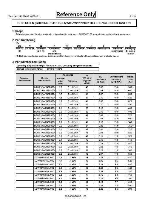
CHIP COILS (CHIP INDUCTORS) LQW03AW□□□□00□ REFERENCE SPECIFICATION1. ScopeThis reference specification applies to chip coils (chip inductors) LQW03AW_00 series for general electronic equipment.2. Part Numbering(Ex.)LQ W 03 A W 5N4 J 0 0 DProductID Structure Dimension(L × W)ApplicationandcharacteristicCategory Inductance Tolerance Performance ElectrodespecificationPackagingD: taping*B: bulk*B: Bulk packing is also available (taping condition: however, products without reels are put in plastic bags).3. Part Number and RatingOperating temperature range -55°C to +125°C (including self-generated heat)Storage temperature range -55°C to +125°CCustomer Part numberMurataPart numberInductance Q(900 MHz)(Typicalvalue)DCresistance(Ω max.)Self-resonantfrequency(GHz min.)Ratedcurrent(mA) Nominalvalue(nH)ToleranceLQW03AW1N0C00D1.0C:±0.2nH 48 0.03 19.0 900 LQW03AW1N1C00D1.1C:±0.2nH 41 0.06 19.0 660 LQW03AW1N7C00D1.7C:±0.2nH 41 0.07 19.0 600 LQW03AW1N8C00D1.8C:±0.2nH 37 0.10 19.0 520 LQW03AW1N9C00D1.9C:±0.2nH 41 0.08 19.0 620 LQW03AW2N0C00D2.0C:±0.2nH 42 0.10 19.0 490 LQW03AW2N1C00D2.1C:±0.2nH 35 0.16 19.0 400 LQW03AW2N2C00D2.2C:±0.2nH 33 0.16 19.0 400 LQW03AW2N7C00D2.7C:±0.2nH 46 0.06 15.0 720 LQW03AW2N8C00D2.8C:±0.2nH 44 0.08 14.0 600 LQW03AW2N9C00D2.9C:±0.2nH 41 0.10 13.0 540 LQW03AW3N0C00D3.0C:±0.2nH 34 0.22 14.0 350 LQW03AW3N1C00D3.1C:±0.2nH 48 0.07 12.0 720 LQW03AW3N2C00D3.2C:±0.2nH 48 0.08 10.0 580 LQW03AW3N3C00D3.3C:±0.2nH 47 0.11 11.0 520 LQW03AW3N4C00D3.4C:±0.2nH 43 0.15 11.0 440 LQW03AW3N5C00D3.5C:±0.2nH 43 0.15 12.0 440 LQW03AW3N6C00D3.6C:±0.2nH 36 0.23 11.0 340 LQW03AW3N7C00D3.7C:±0.2nH 38 0.23 11.0 340 LQW03AW3N9C00D3.9C:±0.2nH 48 0.07 11.0 650 LQW03AW4N3J00D4.3 J:±5% 45 0.12 11.0 480 LQW03AW4N7J00D4.7 J:±5% 45 0.09 9.5 620 LQW03AW5N1J00D5.1 J:±5% 45 0.14 9.5 480 LQW03AW5N4J00D5.4 J:±5% 46 0.21 9.5 420 LQW03AW5N6J00D5.6 J:±5% 37 0.33 8.3 330 LQW03AW5N8J00D5.8 J:±5% 47 0.16 8.8 460 LQW03AW6N2J00D6.2 J:±5% 39 0.22 9.9 360 LQW03AW6N8J00D6.8 J:±5% 42 0.18 7.7 460 LQW03AW7N5J00D7.5 J:±5% 41 0.24 7.5 400 LQW03AW8N2J00D8.2 J:±5% 40 0.26 8.5 290Customer Part numberMurataPart numberInductance Q(900 MHz)(Typicalvalue)DCresistance(Ω max.)Self-resonantfrequency(GHz min.)Ratedcurrent(mA)Nominalvalue(nH)ToleranceLQW03AW8N7J00D8.7J:±5% 39 0.42 7.5 290 LQW03AW9N1J00D9.1J:±5% 46 0.22 6.4 460 LQW03AW10NJ00D10.0J:±5% 37 0.46 7.2 250 LQW03AW11NJ00D11.0J:±5% 37 0.47 7.0 260 LQW03AW12NJ00D12.5J:±5% 39 0.54 6.0 280 LQW03AW13NJ00D13.0J:±5% 39 0.54 5.9 280 LQW03AW14NJ00D13.5J:±5% 37 0.53 6.0 240 LQW03AW15NJ00D15.5J:±5% 38 0.60 5.7 230 4. Testing ConditionsUnless otherwise specified Temperature: ordinary temperature (15°C to 35°C)Humidity: ordinary humidity [25% to 85% (RH)]In case of doubt Temperature: 20°C±2°CHumidity: 60% to 70% (RH)Atmospheric pressure: 86 kPa to 106 kPa5. Appearance and DimensionsUnit mass (typical value): 0.23 mg6. MarkingNo marking.7. Electrical PerformanceNo.ItemSpecificationTest method7.1 InductanceMeet chapter 3 ratings.Measuring equipment: Keysight E4991A or the equivalentMeasuring frequency: Inductance 250 MHz 1.0 nH to 3.9 nH 100 MHz 4.3 nH to 15.5 nH Measuring conditions:Measurement signal level: Approx. 0 dBm Measurement terminal distance: 0.3 mm Electrical length: 10.0 mmMeasuring fixture: Keysight 16197APosition the chip coil under test as shown in the measuring example below and connect it to the electrode by applying weight. Measurement example:Measuring method: see "Electrical performance: Measuring method for inductance/Q" in the chapter"16. Appendix".7.2 QMeet chapter 3 ratings.7.3 DC resistance Meet chapter 3 ratings. Measuring equipment: digital multimeter 7.4 Self-resonantfrequency Meet chapter 3 ratings.Measuring equipment: Keysight N5230A or theequivalent7.5 Rated currentProduct temperature rise: 20°C max.Apply the rated current specified in chapter 3.8. Mechanical PerformanceNo.ItemSpecificationTest method8.1 Bending testNo significant mechanical damage or no sign of electrode peeling off shall be observed. Test substrate: glass-epoxy substrate (100 mm × 40 mm × 0.8 mm) Pressurizing speed: 1 mm/sDeflection: 2 mm Holding time: 5 s8.2 VibrationAppearance shall have no significant mechanical damage.Oscillation frequency: 10 Hz to 55 Hz to 10 Hz, for approx. 1 minTotal amplitude: 1.5 mmTest time: 3 directions perpendicular to each other, 2 h for each direction (6 h in total)No.ItemSpecificationTest method8.3 Solderability90% or more of the outer electrode shall be covered with new solder seamlessly. Flux: immersed in ethanol solution [including anactivator with a chlorine conversion value of 0.06(wt)%]with a rosin content of 25(wt)% for 5 s to 10 s. Solder: Sn-3.0Ag-0.5Cu solderPre-heating: 150°C±10°C/60 s to 90 s Solder temperature: 240°C±5°C Immersion time: 4 s±1 s 8.4 Resistance tosoldering heatAppearance: No significant mechanical damage shall be observed.Inductance change rate: within ±5%Flux: immersed in ethanol solution [including anactivator with a chlorine conversion value of 0.06(wt)%] with a rosin content of 25(wt)% for 5 s to 10 s. Solder: Sn-3.0Ag-0.5Cu solderPre-heating: 150°C±10°C/60 s to 90 s Solder temperature: 270°C±5°C Immersion time: 5 s±1 sPost-treatment: left at a room condition for 24 h±2 h9. Environmental PerformanceThe product is soldered on a substrate for test. No. Item Specification Test method9.1 Heat resistanceAppearance: No significant mechanicaldamage shall be observed.Inductance change rate: within ±5%Q change rate: within ±20%Temperature: 125°C±2°CTest time: 1000 h (+48 h, -0 h)Post-treatment: left at a room condition for 24 h±2 h 9.2 Cold resistanceAppearance: No significant mechanical damage shall be observed.Inductance change rate: within ±5% Q change rate: within ±20%Temperature: -55°C±2°CTest time: 1000 h (+48 h, -0 h)Post-treatment: left at a room condition for 24 h±2 h9.3 HumidityAppearance: No significant mechanical damage shall be observed.Inductance change rate: within ±5% Q change rate: within ±20%Temperature: 70°C±2°CHumidity: 90% (RH) to 95% (RH) Test time: 1000 h (+48 h, -0 h)Post-treatment: left at a room condition for 24 h±2 h 9.4 Temperature cycle Appearance: No significant mechanicaldamage shall be observed.Inductance change rate: within ±5% Q change rate: within ±20%Single cycle conditions:Step 1: -55°C±2°C/30 min±3 minStep 2: ordinary temperature/10 min to 15 min Step 3: +125°C±2°C/30 min±3 minStep 4: ordinary temperature/10 min to 15 min Number of testing: 10 cyclesPost-treatment: left at a room condition for 24 h±2 h10. Specification of Packaging10.1 Appearance and dimensions of tape (8 mm width/paper tape)A (0.52)B (0.65) t 0.75 max.(in mm)10.2 Taping specificationsPacking quantity (Standard quantity) 10000 pcs/reelPacking method The products are placed in embossed cavities of a base tape and sealed by a cover tape.Feed hole position The feed holes on the base tape are on the right side when the cover tape is pulled toward the user. JointThe base tape and the cover tape are seamless.Number of missing productsNumber of missing products within 0.025% of the number per reel or 1 pc., whichever is greater, and are not continuous. The specified quantity per reel is kept.10.3 Break down force of tapeBreak down force of cover tape5 N min.10.4 Peeling off force of cover tapeSpeed of peeling off 300 mm/minPeeling off force0.1 N to 0.6 N (The lower limit is for typical value.)10.5 Dimensions of leader section, trailer section and reelA vacant section is provided in the leader (start) section and trailer (end) section of the tape for the product. The leader section is further provided with an area consisting only of the cover tape (or top tape). (See the diagram below.)10.6 Marking for reelCustomer part number, Murata part number, inspection number (*1), RoHS marking (*2), quantity, etc. *1 Expression of inspection No.: □□ ○○○○(1) (2) (3)(1) Factory code(2) Date First digit: year/last digit of yearSecond digit: month/Jan. to Sep.→1 to 9, Oct. to Dec.→O, N, D Third, Fourth digit: day (3) Serial No.*2 Expression of RoHS marking: ROHS- Y ( ) (1) (2)(1) RoHS regulation conformity(2) Murata classification number10.7 Marking on outer box (corrugated box)Customer name, purchasing order number, customer part number, Murata part number, RoHS marking (*2), quantity, etc.FCover tapetape165°to 180゜10.8 Specification of outer boxDimensions of outer box(mm) Standard reel quantity in outer box (reel)WDH186 186 935* Above outer box size is typical. It depends on a quantity of an order.11. Caution11.1 Restricted applicationsPlease contact us before using our products for the applications listed below which require especially high reliability for the prevention of defects which might directly cause damage to the third party's life, body or property. (1) Aircraft equipment (2) Aerospace equipment (3) Undersea equipment (4) Power plant controlequipment(5) Medical equipment (6) Transportation equipment (vehicles, trains, ships, etc.) (7) Traffic signal equipment (8) Disaster/crimeprevention equipment(9) Data-processing equipment (10) Applications of similar complexity and/or reliability requirements to the applications listed in the above11.2 Precautions on ratingAvoid using in exceeded the rated temperature range, rated voltage, or rated current.Usage when the ratings are exceeded could lead to wire breakage, burning, or other serious fault.11.3 Inrush currentIf an inrush current (or pulse current or rush current) that significantly exceeds the rated current is applied to the product, overheating could occur, resulting in wire breakage, burning, or other serious fault.11.4 Corrosive gasPlease refrain from use since contact with environments with corrosive gases (sulfur gas [hydrogen sulfide, sulfur dioxide, etc.], chlorine, ammonia, etc.) or oils (cutting oil, silicone oil, etc.) that have come into contact with the previously stated corrosive gas environment will result in deterioration of product quality or an open from deterioration due to corrosion of product electrode, etc. We will not bear any responsibility for use under these environments.12. Precautions for UseThis product is for use only with reflow soldering. It is designed to be mounted by soldering. If you want to use other mounting method, for example, using a conductive adhesive, please consult us beforehand.Also, if repeatedly subjected to temperature cycles or other thermal stress, due to the difference in the coefficient of thermal expansion with the mounting substrate, the solder (solder fillet part) in the mounting part may crack.The occurrence of cracks due to thermal stress is affected by the size of the land where mounted, the solder volume, and the heat dissipation of the mounting substrate. Carefully design it when a large change in ambient temperature is assumed.12.1 Land dimensionsThe following diagram shows the recommended land dimensions for reflow soldering.The land dimensions are designed in consideration of electrical characteristics and mountability. Use of other landdimensions may preclude achievement of performance. In some cases, it may result in poor solderability, including positional shift. If you use other land pattern, consider it adequately.a 0.23b 0.65c 0.4(in mm)WDLabelH12.2 Flux and solder usedFlux• Use a rosin-based flux that includes an activator with a chlorine conversion value of 0.06(wt)% to 0.1(wt)%. • Do not use a highly acidic flux with a halide content exceeding 0.2(wt)% (chlorine conversion value). • Do not use a water-soluble flux.Solder• Use Sn-3.0Ag-0.5Cu solder.• Standard thickness of solder paste: 80 μm to 100 μmIf you want to use a flux other than the above, please consult our technical department.12.3 Soldering conditions (reflow)• Pre-heating should be in such a way that the temperature difference between solder and product surface is limited to 150°C max.Cooling into solvent after soldering also should be in such a way that the temperature difference is limited to 100°C max. Insufficient pre-heating may cause cracks on the product, resulting in the deterioration of product quality. • Standard soldering profile and the limit soldering profile is as follows.The excessive limit soldering conditions may cause leaching of the electrode and/or resulting in the deterioration of product quality.Standard profile Limit profilePre-heating 150°C to 180°C/90 s±30 s 150°C to 180°C/90 s±30 s HeatingAbove 220°C/30 s to 60 sAbove 230°C/60 s max.Peak temperature 245°C±3°C 260°C/10 s Number of reflow cycles2 times2 times12.4 Reworking with soldering ironDo not perform reworking with a soldering iron on this product.12.5 Solder volumeSolder shall be used not to increase the volume too much.An increased solder volume increases mechanical stress on the product. Exceeding solder volume may cause the failure of mechanical or electrical performance.Limit ProfileStandard Profile90s±30s230℃260℃245℃±3℃220℃30s~60s60s max.180150Temp.(s)(℃)Time.12.6 Product's locationThe following shall be considered when designing and laying out PCBs.(1) PCB shall be designed so that products are not subject to mechanical stress due to warping the board. [Products direction]Products shall be located in the sideways direction (length: a < b) to the mechanical stress.(2) Components location on PCB separationIt is effective to implement the following measures, to reduce stress in separating the board.It is best to implement all of the following three measures; however, implement as many measures as possible to reduce stress.Contents of measures Stress level(1) Turn the mounting direction of the component parallel to theboard separation surface.A > D *1 (2) Add slits in the board separation part.A >B (3) Keep the mounting position of the component away from the board separation surface.A > C*1 A > D is valid when stress is added vertically to the perforation as with hand separation. If a cutting disc is used, stress will be diagonal to the PCB, therefore A > D is invalid.(3) Mounting components near screw holesWhen a component is mounted near a screw hole, it may be affected by the board deflection that occurs during the tightening of the screw.Mount the component in a position as far away from the screw holes as possible.12.7 Handling of substrateAfter mounting products on a substrate, do not apply any stress to the product caused by bending or twisting to the substrate when cropping the substrate, inserting and removing a connector from the substrate or tightening screw to the substrate. Excessive mechanical stress may cause cracking in the product.Bending Twisting〈Poor example 〉〈Good example〉ba12.8 CleaningThe product shall be cleaned under the following conditions.(1) The cleaning temperature shall be 60°C max. If isopropyl alcohol (IPA) is used, the cleaning temperature shall be 40°Cmax.(2) Perform ultrasonic cleaning under the following conditions. Exercise caution to prevent resonance phenomenon inmounted products and the PCB.Item RequirementPower 20 W/L max.Time 5 min max.Frequency 28 kHz to 40 kHz(3) CleanerAlcohol-based cleaner: IPAAqueous agent: PINE ALPHA ST-100S(4) There shall be no residual flux or residual cleaner. When using aqueous agent, rinse the product with deionized wateradequately and completely dry it so that no cleaner is left.* For other cleaning, consult our technical department.12.9 Storage and transportationStorage period Use the product within 12 months after delivery.If you do not use the product for more than 12 months, check solderability before using it.Storage conditions • The products shall be stored in a room not subject to rapid changes in temperature and humidity.The recommended temperature range is -10°C to +40°C. The recommended relative humidityrange is 15% to 85%.Keeping the product in corrosive gases, such as sulfur, chlorine gas or acid, oxidizes theelectrode, resulting in poor solderability or corrosion of the coil wire of the product.• Do not keep products in bulk packaging. Doing so may cause collision between the products orbetween the products and other products, resulting in core chipping or wire breakage.• Do not place the products directly on the floor; they should be placed on a palette so that they arenot affected by humidity or dust.• Avoid keeping the products in a place exposed to direct sunlight, heat or vibration.Transportation Excessive vibration and impact reduces the reliability of the products. Exercise caution whenhandling the products.12.10 Resin coatingThe inductance value may change due to high cure-stress of resin to be used for coating/molding products.A wire breakage issue may occur by mechanical stress caused by the resin, amount/cured shape of resin, or operatingcondition etc. Some resin contains some impurities or chloride possible to generate chlorine by hydrolysis under some operating condition may cause corrosion of wire of coil, leading to wire breakage.So, please pay your careful attention when you select resin in case of coating/molding the products with the resin.Prior to use the coating resin, please make sure no reliability issue is observed by evaluating products mounted on your board.12.11 Handling of product• Sharp material such as a pair of tweezers or other material such as bristles of cleaning brush, shall not be touched to the winding portion to prevent the breaking of wire.• Mechanical shock should not be applied to the products mounted on the board to prevent the breaking of the core.12.12 Handling with mounting equipment• With some types of mounting equipment, a support pin pushes up the product from the bottom of the base (paper) tape when the product is sucked with the pick-up nozzle.When using this type of equipment, detach the support pin to prevent the breaking of wire on the product.• In some cases, the laser recognition function of the mounting equipment may not recognize this product correctly.Please contact us when using laser recognition. (There is no problem with the permeation and reflection type.)13. Note(1) Please make sure that your product has been evaluated in view of your specifications with our product being mounted toyour product.(2) You are requested not to use our product deviating from the reference specifications.(3) The contents of this reference specification are subject to change without advance notice. Please approve our productspecifications or transact the approval sheet for product specifications before ordering.14. AppendixElectrical performance: Measuring method for inductance/Q (Q measurement is applicable only when the Q value is included in the rating table.)Perform measurement using the method described below. (Perform correction for the error deriving from the measuring terminal.)(1) Residual elements and stray elements of the measuring terminal can be expressed by the F parameter for the 2-poleterminal as shown in the figure below.(2) The product's impedance value (Zx) and measured impedance value (Zm) can be expressed as shown below, by usingthe respective current and voltage for input/output.Zm=V1I1Zx=V2I2(3) Thus, the relationship between the product's impedance value (Zx) and measured impedance value (Zm) is as follows.Zx=αZm-β1-ZmΓHere,α=D/A=1β=B/D=Zsm - (1 - Yom Zsm) ZssΓ=C/A=YomZsm: measured impedance of short chipZss: residual impedance of short chip (0.480 nH)Yom: measured admittance when measuring terminal is open (4) Calculate inductance Lx and Qx using the equations shown below.Lx=Im (Zx)2πfLx: inductance of chip coilQx: Q of chip coilf: measuring frequencyQx=Im (Zx) Re (Zx)。
超低功耗微型超声时间差测距传感器CH101说明书
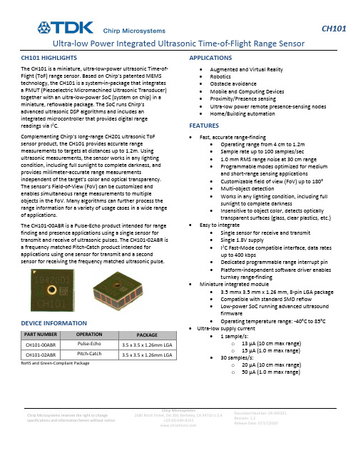
CH101 Ultra-low Power Integrated Ultrasonic Time-of-Flight Range SensorChirp Microsystems reserves the right to change specifications and information herein without notice.Chirp Microsystems2560 Ninth Street, Ste 200, Berkeley, CA 94710 U.S.A+1(510) 640–8155Document Number: DS-000331Revision: 1.2Release Date: 07/17/2020CH101 HIGHLIGHTSThe CH101 is a miniature, ultra-low-power ultrasonic Time-of-Flight (ToF) range sensor. Based on Chirp’s patented MEMS technology, the CH101 is a system-in-package that integrates a PMUT (Piezoelectric Micromachined Ultrasonic Transducer) together with an ultra-low-power SoC (system on chip) in a miniature, reflowable package. The SoC runs Chirp’s advanced ultrasonic DSP algorithms and includes an integrated microcontroller that provides digital range readings via I2C.Complementing Chirp’s long-range CH201 ultrasonic ToF sensor product, the CH101 provides accurate range measurements to targets at distances up to 1.2m. Using ultrasonic measurements, the sensor works in any lighting condition, including full sunlight to complete darkness, and provides millimeter-accurate range measurements independent of the target’s color and optical transparency. The sensor’s Field-of-View (FoV) can be customized and enables simultaneous range measurements to multiple objects in the FoV. Many algorithms can further process the range information for a variety of usage cases in a wide range of applications.The CH101-00ABR is a Pulse-Echo product intended for range finding and presence applications using a single sensor for transmit and receive of ultrasonic pulses. The CH101-02ABR is a frequency matched Pitch-Catch product intended for applications using one sensor for transmit and a second sensor for receiving the frequency matched ultrasonic pulse.DEVICE INFORMATIONPART NUMBER OPERATION PACKAGECH101-00ABR Pulse-Echo 3.5 x 3.5 x 1.26mm LGA CH101-02ABR Pitch-Catch 3.5 x 3.5 x 1.26mm LGA RoHS and Green-Compliant Package APPLICATIONS•Augmented and Virtual Reality•Robotics•Obstacle avoidance•Mobile and Computing Devices•Proximity/Presence sensing•Ultra-low power remote presence-sensing nodes •Home/Building automation FEATURES•Fast, accurate range-finding•Operating range from 4 cm to 1.2m•Sample rate up to 100 samples/sec• 1.0 mm RMS range noise at 30 cm range•Programmable modes optimized for medium and short-range sensing applications•Customizable field of view (FoV) up to 180°•Multi-object detection•Works in any lighting condition, including full sunlight to complete darkness•Insensitive to object color, detects opticallytransparent surfaces (glass, clear plastics, etc.) •Easy to integrate•Single sensor for receive and transmit•Single 1.8V supply•I2C Fast-Mode compatible interface, data rates up to 400 kbps•Dedicated programmable range interrupt pin•Platform-independent software driver enables turnkey range-finding•Miniature integrated module• 3.5 mmx 3.5 mm x 1.26 mm, 8-pin LGA package•Compatible with standard SMD reflow•Low-power SoC running advanced ultrasound firmware•Operating temperature range: -40°C to 85°C •Ultra-low supply current• 1 sample/s:o13 µA (10 cm max range)o15 µA (1.0 m max range)•30 samples/s:o20 µA (10 cm max range)o50 µA (1.0 m max range)Table of ContentsCH101 Highlights (1)Device Information (1)Applications (1)Features (1)Simplified Block Diagram (3)Absolute Maximum Ratings (4)Package Information (5)8-Pin LGA (5)Pin Configuration (5)Pin Descriptions (6)Package Dimensions (6)Electrical Characteristics (7)Electrical Characteristics (Cont’d) (8)Typical Operating Characteristics (9)Detailed Description (10)Theory of Operation (10)Device Configuration (10)Applications (11)Chirp CH101 Driver (11)Object Detection (11)Interfacing to the CH101 Ultrasonic Sensor (11)Device Modes of Operation: (12)Layout Recommendations: (13)PCB Reflow Recommendations: (14)Use of Level Shifters (14)Typical Operating Circuits (15)Ordering Information (16)Part Number Designation (16)Package Marking (17)Tape & Reel Specification (17)Shipping Label (17)Revision History (19)SIMPLIFIED BLOCK DIAGRAMFigure 1. Simplified Block DiagramABSOLUTE MAXIMUM RATINGSPARAMETER MIN. TYP. MAX. UNIT AVDD to VSS -0.3 2.2 V VDD to VSS -0.3 2.2 V SDA, SCL, PROG, RST_N to VSS -0.3 2.2 V Electrostatic Discharge (ESD)Human Body Model (HBM)(1)Charge Device Model (CDM)(2)-2-5002500kVV Latchup -100 100 mA Temperature, Operating -40 85 °C Relative Humidity, Storage 90 %RH Continuous Input Current (Any Pin) -20 20 mA Soldering Temperature (reflow) 260 °CTable 1. Absolute Maximum RatingsNotes:1.HBM Tests conducted in compliance with ANSI/ESDA/JEDEC JS-001-2014 Or JESD22-A114E2.CDM Tests conducted in compliance with JESD22-C101PACKAGE INFORMATION8-PIN LGADESCRIPTION DOCUMENT NUMBER CH101 Mechanical Integration Guide AN-000158CH101 and CH201 Ultrasonic Transceiver Handling andAssembly Guidelines AN-000159Table 2. 8-Pin LGAPIN CONFIGURATIONTop ViewFigure 2. Pin Configuration (Top View)PIN DESCRIPTIONSPIN NAME DESCRIPTION1 INT Interrupt output. Can be switched to input for triggering and calibration functions2 SCL SCL Input. I2C clock input. This pin must be pulled up externally.3 SDA SDA Input/Output. I2C data I/O. This pin must be pulled up externally.4 PROG Program Enable. Cannot be floating.5 VSS Power return.6 VDD Digital Logic Supply. Connect to externally regulated 1.8V supply. Suggest commonconnection to AVDD. If not connected locally to AVDD, b ypass with a 0.1μF capacitor asclose as possible to VDD I/O pad.7 AVDD Analog Power Supply. Connect to externally re gulated supply. Bypass with a 0.1μFcapacitor as close as possible to AVDD I/O pad.8 RESET_N Active-low reset. Cannot be floating.Table 3. Pin DescriptionsPACKAGE DIMENSIONSFigure 3. Package DimensionsELECTRICAL CHARACTERISTICSAVDD = VDD = 1.8VDC, VSS = 0V, T A = +25°C, min/max are from T A = -40°C to +85°C, unless otherwise specified.PARAMETER SYMBOL CONDITIONS MIN TYP MAX UNITSPOWER SUPPLYAnalog Power Supply AVDD 1.62 1.8 1.98 V Digital Power Supply VDD 1.62 1.8 1.98 VULTRASONIC TRANSMIT CHANNELOperating Frequency 175 kHzTXRX OPERATION (GPR FIRMWARE USED UNLESS OTHERWISE SPECIFIED)Maximum Range Max Range Wall Target58 mm Diameter Post1.2(1)0.7mm Minimum Range Min Range Short-Range F/W used 4(2)cm Measuring Rate (Sample/sec) SR 100 S/s Field of View FoV Configurable up to 180º deg Current Consumption (AVDD +VDD) I SSR=1S/s, Range=10 cmSR=1S/s, Range=1.0mSR=30S/s, Range=10 cmSR=30S/s, Range=1.0m13152050μAμAμAμA Range Noise N R Target range = 30 cm 1.0 mm, rms Measurement Time 1m max range 18 ms Programming Time 60 msTable 4. Electrical CharacteristicsNotes:1.Tested with a stationary target.2.For non-stationary objects. While objects closer than 4cm can be detected, the range measurement is not ensured.ELECTRICAL CHARACTERISTICS (CONT’D)AVDD = VDD = 1.8VDC, VSS = 0V, T A = +25°C, unless otherwise specified.PARAMETERSYMBOL CONDITIONS MINTYP MAX UNITS DIGITAL I/O CHARACTERISTICS Output Low Voltage V OL SDA, INT,0.4 V Output High Voltage V OH INT 0.9*V VDD V I 2C Input Voltage Low V IL_I2C SDA, SCL 0.3*V VDDV I 2C Input Voltage High V IH_I2C SDA, SCL 0.7*V VDD V Pin Leakage Current I L SDA,SCL, INT(Inactive), T A =25°C±1μA DIGITAL/I 2C TIMING CHARACTERISTICSSCL Clock Frequencyf SCLI 2C Fast Mode400kHzTable 5. Electrical Characteristics (Cont’d)TYPICAL OPERATING CHARACTERISTICSAVDD = VDD = 1.8VDC, VSS = 0V, T A = +25°C, unless otherwise specified.Typical Beam Pattern – MOD_CH101-03-01 Omnidirectional FoV module(Measured with a 1m2 flat plate target at a 30 cm range)Figure 4. Beam pattern measurements of CH101 moduleDETAILED DESCRIPTIONTHEORY OF OPERATIONThe CH101 is an autonomous, digital output ultrasonic rangefinder. The Simplified Block Diagram, previously shown, details the main components at the package-level. Inside the package are a piezoelectric micro-machined ultrasonic transducer (PMUT) and system-on-chip (SoC). The SoC controls the PMUT to produce pulses of ultrasound that reflect off targets in the sensor’s Field of View (FoV). The reflections are received by the same PMUT after a short time delay, amplified by sensitive electronics, digitized, and further processed to produce the range to the primary target. Many algorithms can further process the range information for a variety of usage cases in a wide range of applications.The time it takes the ultrasound pulse to propagate from the PMUT to the target and back is called the time-of-flight (ToF). The distance to the target is found by multiplying the time-of-flight by the speed of sound and dividing by two (to account for the round-trip). The speed of sound in air is approximately 343 m/s. The speed of sound is not a constant but is generally stable enough to give measurement accuracies within a few percent error.DEVICE CONFIGURATIONA CH101 program file must be loaded into the on-chip memory at initial power-on. The program, or firmware, is loaded through a special I2C interface. Chirp provides a default general-purpose rangefinder (GPR) firmware that is suitable for a wide range of applications. This firmware enables autonomous range finding operation of the CH101. It also supports hardware-triggering of the CH101 for applications requiring multiple transceivers. Program files can also be tailored to the customer’s application. Contact Chirp for more information.CH101 has several features that allow for low power operation. An ultra-low-power, on-chip real-time clock (RTC) sets the sample rate and provides the reference for the time-of-flight measurement. The host processor does not need to provide any stimulus to the CH101 during normal operation, allowing the host processor to be shut down into its lowest power mode until the CH101 generates a wake-up interrupt. There is also a general-purpose input/output (INT) pin that is optimized to be used as a system wake-up source. The interrupt pin can be configured to trigger on motion or proximity.APPLICATIONSCHIRP CH101 DRIVERChirp provides a compiler and microcontroller-independent C driver for the CH101 which greatly simplifies integration. The CH101 driver implements high-level control of one or more CH101s attached to one or more I2C ports on the host processor. The CH101 driver allows the user to program, configure, trigger, and readout data from the CH101 through use of C function calls without direct interaction with the CH101 I2C registers. The CH101 driver only requires the customer to implement an I/O layer which communicates with the host processor’s I2C hardware and GPIO hardware. Chirp highly recommends that all designs use the CH101 driver.OBJECT DETECTIONDetecting the presence of objects or people can be optimized via software, by setting the sensor’s full-scale range (FSR), and via hardware, using an acoustic housing to narrow or widen the sensor’s field-of-view. The former means that the user may set the maximum distance at which the sensor will detect an object. FSR values refer to the one-way distance to a detected object.In practice, the FSR setting controls the amount of time that the sensor spends in the listening (receiving) period during a measurement cycle. Therefore, the FSR setting affects the time required to complete a measurement. Longer full-scale range values will require more time for a measurement to complete.Ultrasonic signal processing using the CH101’s General Purpose Rangefinder (GPR) Firmware will detect echoes that bounce off the first target in the Field-of-View. The size, position, and material composition of the target will affect the maximum range at which the sensor can detect the target. Large targets, such as walls, are much easier to detect than smaller targets. Thus, the associated operating range for smaller targets will be shorter. The range to detect people will be affected by a variety of factors such as a person’s size, clothing, orientation to the sensor and the sensor’s field-of-view. In general, given these factors, people can be detected at a maximum distance of 0.7m from the CH101 sensor.For additional guidance on the detection of people/objects using the NEMA standard, AN-000214 Presence Detection Application Note discusses the analysis of presence detection using the Long-Range CH201 Ultrasonic sensor.INTERFACING TO THE CH101 ULTRASONIC SENSORThe CH101 communicates with a host processor over the 2-wire I2C protocol. The CH101 operates as an I2C slave and responds to commands issued by the I2C master.The CH101 contains two separate I2C interfaces, running on two separate slave addresses. The first is for loading firmware into the on-chip program memory, and the second is for in-application communication with the CH101. The 7-bit programming address is0x45, and the 7-bit application address default is 0x29. The application address can be reprogrammed to any valid 7-bit I2C address. The CH101 uses clock stretching to allow for enough time to respond to the I2C master. The CH101 clock stretches before the acknowledge (ACK) bit on both transmit and receive. For example, when the CH101 transmits, it will hold SCL low after it transmits the 8th bit from the current byte while it loads the next byte into its internal transmit buffer. When the next byte is ready, it releases the SCL line, reads the master’s ACK bit, and proceeds accordingly. When the CH101 is receiving, it holds the SCL line low after it receives the 8th bit in a byte. The CH101 then chooses whether to ACK or NACK depending on the received data and releases the SCL line.The figure below shows an overview of the I2C slave interface. In the diagram, ‘S’ indicates I2C start, ‘R/W’ is the read/write bit, ‘Sr’ is a repeated start, ‘A’ is acknowledge, and ‘P’ is the stop condition. Grey boxes indicate the I2C master actions; white boxes indicate the I2C slave actions.Figure 5. CH101 I2C Slave Interface DiagramDEVICE MODES OF OPERATION:FREE-RUNNING MODEIn the free-running measurement mode, the CH101 runs autonomously at a user specified sample rate. In this mode, the INT pin is configured as an output. The CH101 pulses the INT pin high when a new range sample is available. At this point, the host processor may read the sample data from the CH101 over the I2C interface.HARDWARE-TRIGGERED MODEIn the hardware triggered mode, the INT pin is used bi-directionally. The CH101 remains in an idle condition until triggered by pulsing the INT pin. The measurement will start with deterministic latency relative to the rising edge on INT. This mode is most useful for synchronizing several CH101 transceivers. The host controller can use the individual INT pins of several transceivers to coordinate the exact timing.CH101 BEAM PATTERNSThe acoustic Field of View is easily customizable for the CH101 and is achieved by adding an acoustic housing to the transceiver that is profiled to realize the desired beam pattern. Symmetric, asymmetric, and omnidirectional (180° FoV) beam patterns are realizable. An example beam pattern is shown in the Typical Operating Characteristics section of this document and several acoustic housing designs for various FoV’s are available from Chirp.LAYOUT RECOMMENDATIONS:RECOMMENDED PCB FOOTPRINTDimensions in mmFigure 6. Recommended PCB FootprintPCB REFLOW RECOMMENDATIONS:See App Note AN-000159, CH101 and CH201 Ultrasonic Transceiver Handling and Assembly Guidelines.USE OF LEVEL SHIFTERSWhile the use of autosense level shifters for all the digital I/O signal signals is acceptable, special handling of the INT line while using a level shifter is required to ensure proper resetting of this line. As the circuit stage is neither a push-pull nor open-drain configuration (see representative circuit below), it is recommended that level shifter with a manual direction control line be used. The TI SN74LVC2T45 Bus Transceiver is a recommended device for level shifting of the INT signal line.Figure 7. INT Line I/O Circuit StageTYPICAL OPERATING CIRCUITSFigure 8. Single Transceiver OperationFigure 9. Multi- Transceiver OperationORDERING INFORMATIONPART NUMBER DESIGNATIONFigure 10. Part Number DesignationThis datasheet specifies the following part numbersPART NUMBER OPERATION PACKAGE BODY QUANTITY PACKAGING CH101-00ABR Pulse-Echo 3.5 mm x 3.5 mm x 1.26 mmLGA-8L 1,000 7” Tape and ReelCH101-02ABR Pitch-Catch 3.5 mm x 3.5 mm x 1.26 mmLGA-8L 1,000 7” Tape and ReelTable 6. Part Number DesignationCH101-xxABxProduct FamilyProduct Variant Shipping CarrierR = Tape & Reel 00AB = Pulse-Echo Product Variant02AB = Pitch-Catch Product VariantCH101 = Ultrasonic ToF SensorPACKAGE MARKINGFigure 11. Package MarkingTAPE & REEL SPECIFICATIONFigure 12. Tape & Reel SpecificationSHIPPING LABELA Shipping Label will be attached to the reel, bag and box. The information provided on the label is as follows:•Device: This is the full part number•Lot Number: Chirp manufacturing lot number•Date Code: Date the lot was sealed in the moisture proof bag•Quantity: Number of components on the reel•2D Barcode: Contains Lot No., quantity and reel/bag/box numberDimensions in mmDEVICE: CH101-XXXXX-XLOT NO: XXXXXXXXDATE CODE: XXXXQTY: XXXXFigure 13. Shipping LabelREVISION HISTORY09/30/19 1.0 Initial Release10/22/19 1.1 Changed CH-101 to CH101. Updated figure 7 to current markings.07/17/20 1.2 Format Update. Incorporated “Maximum Ratings Table” and “Use of LevelShifters” section.This information furnished by Chirp Microsystems, Inc. (“Chirp Microsystems”) is believed to be accurate and reliable. However, no responsibility is assumed by Chirp Microsystems for its use, or for any infringements of patents or other rights of third parties that may result from its use. Specifications are subject to change without notice. Chirp Microsystems reserves the right to make changes to this product, including its circuits and software, in order to improve its design and/or performance, without prior notice. Chirp Microsystems makes no warranties, neither expressed nor implied, regarding the information and specifications contained in this document. Chirp Microsystems assumes no responsibility for any claims or damages arising from information contained in this document, or from the use of products and services detailed therein. This includes, but is not limited to, claims or damages based on the infringement of patents, copyrights, mask work and/or other intellectual property rights.Certain intellectual property owned by Chirp Microsystems and described in this document is patent protected. No license is granted by implication or otherwise under any patent or patent rights of Chirp Microsystems. This publication supersedes and replaces all information previously supplied. Trademarks that are registered trademarks are the property of their respective companies. Chirp Microsystems sensors should not be used or sold in the development, storage, production or utilization of any conventional or mass-destructive weapons or for any other weapons or life threatening applications, as well as in any other life critical applications such as medical equipment, transportation, aerospace and nuclear instruments, undersea equipment, power plant equipment, disaster prevention and crime prevention equipment.©2020 Chirp Microsystems. All rights reserved. Chirp Microsystems and the Chirp Microsystems logo are trademarks of Chirp Microsystems, Inc. The TDK logo is a trademark of TDK Corporation. Other company and product names may be trademarks of the respective companies with which they are associated.©2020 Chirp Microsystems. All rights reserved.。
ADAPTIVE WRITE ACKNOWLEDGMENT FOR STORAGE DEVICES

专利名称:ADAPTIVE WRITE ACKNOWLEDGMENT FORSTORAGE DEVICES发明人:Bishwajit DUTTA,Sanjeev N. TRIKA,Anand S.RAMALINGAM,Pallav H. GALA申请号:US16855139申请日:20200422公开号:US20200249980A1公开日:20200806专利内容由知识产权出版社提供专利附图:摘要:Examples include techniques for managing high priority (HP) and low priority (LP) write transaction requests by a storage device. An embodiment includes receiving, ata storage controller for a storage device, a write transaction request from a requestor to write data to one or more memory devices in the storage device. When the write transaction request is for a high priority (HP) write, coalescing the write data into a transaction buffer in a memory of the storage device, sending an acknowledgment for the write transaction request to the requestor, and writing the write data into the one or more memory devices. When the write transaction request is for a low priority (LP) write, writing the write data into the one or more memory devices, and then sending an acknowledgment for the write transaction request to the requestor.申请人:Intel Corporation地址:Santa Clara CA US国籍:US更多信息请下载全文后查看。
- 1、下载文档前请自行甄别文档内容的完整性,平台不提供额外的编辑、内容补充、找答案等附加服务。
- 2、"仅部分预览"的文档,不可在线预览部分如存在完整性等问题,可反馈申请退款(可完整预览的文档不适用该条件!)。
- 3、如文档侵犯您的权益,请联系客服反馈,我们会尽快为您处理(人工客服工作时间:9:00-18:30)。
This paper describes a leasing mechanism to manage storage for checkpoints. Before checkpointing, each process negotiates with a storage manager to determine the size and duration of the lease. Once the lease is agreed upon, a process can use the allocated storage for checkpoints. Storage space is returned to the manager when the lease expires. The process is allowed to request renewal of the lease before expiration. The storage manager may accept or decline the request based on management protocols. The leasing mechanism not only manages stable storage effectively but also prevents storage retention by failed processes. A coordinated checkpointing protocol integrated with the leasing management is also described in this paper. The checkpointing protocol uses time for coordination to reduce communication
1
checkpointing is integrated with leasing to reduce the number of messages for establishing consistent global states. The checkpointing mechanism makes use of a three-level storage hierarchy to improve checkpointing performance.
Adaptive Checkpointing with Storage Management for Mobile Environments
Kuo-Feng Ssu University of Illinois, Urbana
Bin Yao Purdue University, West Lafayette
2
1 INTRODUCTION
Wireless networking [1] is an enabling technology for mobile computing. Wireless signals are subject to dispersion and interference, and thus wireless communication is inherently susceptible to data loss and disconnection. The challenges to dependable mobile computing include but are not limited to varying communication bandwidths, high failure rates, frequent disconnections, heterogeneous networks, security risks, limited battery power, and host mobility [2–4]. It is not appropriate to directly apply many of the checkpointing and recovery protocols [5–11] designed for fixed network distributed systems to mobile environments.
W. Kent Fuchs, Fellow IEEE Purdue University, West Lafayette
Nuno Ferreira Neves University of Lisbon, Lisbon
Key Words – Mobile recovery, Storage management, Checkpointing, Recovery. Summary & Conclusions – The limited stable storage available in mobile computing environments can make traditional checkpointing and message logging unsuitable. Since storage on a mobile host is not considered stable, most protocols designed for these environments save the checkpoints on base stations. Previous approaches have assumed that the base station always has sufficient disk space for storing checkpoints. If there is not enough storage available, checkpoints may need to be aborted. This paper describes an adaptive protocol that manages storage for base stations. The protocol integrates leasing storage management with a time-based coordinated checkpointing mechanism. The leasing enables storage managers to effectively control disk space. Leasing prevents hanged processes from indefinitely retaining storage and, in addition, garbage collection is simple. Time-based
3Leabharlann overhead. The protocol also dynamically adjusts the locations used to store checkpoints in order to reduce transmission overhead.
Our experiments were implemented and evaluated in a specific wireless mobile network. The experimental results show that the adaptive checkpointing protocol achieved better performance through hierarchical checkpoint arrangements. Four negotiation protocols with the leasing mechanism were also evaluated. The results demonstrate that the adaptive protocol effectively managed the desired storage allocation for base stations utilizing the four negotiation protocols.
Performance was evaluated by both implementation experiments and simulations. The results show that the adaptive protocol reduces checkpointing overhead and the leasing mechanism maintains the desired storage assignment for base stations.