HE1160电量指示芯片规格书赫尔半导体HEERMICR
HE9193_V1.1中文规格书赫尔半导体HEERMICR

概述HE 9193系列是高纹波抑制率、低功耗、低压差,具有过流和短路保护的CMOS 降压型电压稳压器。
这些器件具有很低的静态偏置电流(70μA Typ.),它们能在输入、输出电压差极小的情况下提300mA 的输出电流,并且仍能保持良好的调整率。
由于输入输出间的电压差很小和静态偏置电流很小,这些器件特别适用于希望延长有用电池寿命的电池供电类产品,如计算机、消费类产品和工业设备等。
特点◆输出范围:1.2V-3.6V ◆300mA 输出电流◆高电源抑制比:70分贝1千赫◆极低的静态偏置电流: 70uA (典型) ◆在关机模式下小于1μA ◆交界处的温度运作为-40°C 至+85°C应用范围◆CDMA / GSM 移动电话◆PDAs/MP3◆WLAN 和蓝牙设备 ◆无绳电话 ◆电池供电系统HE 9193采用SOT-23-5L 、SOT-23-3L 封装典型应用INPUT选型指南HE 9193 X XX XX X 公司标志产品型号版本号输出电压指封装形式L5指SOT-23-5L 如:如:L3指SOT-23-3L 12指1.2V 15指1.5V 18指1.8V 25指2.5V 28指2.8V 30指3.0V 33指3.3V 脚位形状36指3.6V300mA Low Power LDO管脚分布图GNDVINCESOT-23-5L GNDVOUTVDD SOT-23-3L 丝印说明管脚描述300mA Low Power LDO极限参数封装耗散等级结构框图(Vin=Vout+1V,Cin=1uF~10uF,Cout=1uF~10uF,Ta=25℃。
除特别指定)1、OUT2、V OUT (E) :有效输出电压( 即当I OUT保持一定数值,V IN = (V OUT (T)+1.0V)时的输出电压。
3、V dif:V IN1–V OUT(E)’V IN1:逐渐减小输入电压,当输出电压降为V OUT (E)98%时的输入电压。
HE4056E_V2.0中文规格书赫尔半导体HEERMICR

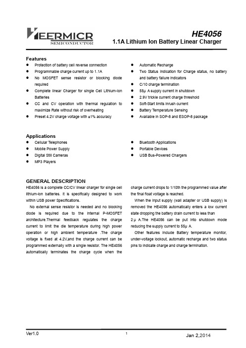
HE4056E_V2.0中文规格书赫尔半导体HEERMICR产品概述HE4056E 是一款完善的单节锂离子电池采用恒流/恒压线性充电电源管理芯片。
专门设计适用于USB 的供电规格。
得益于内部的P-MOSFET 架构,在应用上不需要外部检测电阻。
在大功率运行或高环境温度时,热反馈可以自动调节充电电流以降低芯片温度。
充电电压被限定在4.2V ,充电电流通过外部电阻调节,最大可充1.1A 的充电电流。
在达到目标充电电压后,当充电电流降低到设定值的1/10时,就会自动结束充电过程。
当输入端(交流适配器或USB 电源)拔掉后,自动进入低电流状态,电池漏电流将降到2uA 以下。
还可被设置于停机工作状态,使电源供电电流降到55uA 。
还具备其余特性包括:电池温度检测,充电电流监测,输入欠压闭锁,自动重新充电和充电及充电已满的指示。
功能特性可编程充电电流可达1.1A.实现对单节锂离子电池的完全线性充电管理恒流/恒压充电并具有可在无过热危险的情况下实现充电速率最大化的热调节功能U SB 接口管理单片锂离子电池?预设充电电压为4.2V ?充电电流输出监控?充电状态指示标志?自动重新充电1/10充电电流终止待机模式下的供电电流为55uA ? 2.9V 涓流充电阈值电压?软启动限制了浪涌电流?采用ESOP-8封装应用领域手机,MP3,PDA ?蓝牙应用?USB 接口充电器HE4056E HE4056E HE4056E HE4056E HE4056E HE4056E 1.1A Lithium Ion Battery Linear Charger管脚分布管脚定义HE4056E1.1A Lithium Ion Battery L i near Cha r ger内部框图典型应用电路绝对最大值范围电性参数(V CC =5.0V ,Ta=25℃,除非另有说明)±2-2101 HE4056E1.1A Lithium Ion Battery Linear Charger功能描述HE4056E 是一款完善的单节锂离子电池恒流/恒压线形充电电源管理芯片。
HE63XXM_V1.1中文规格书赫尔半导体HEERMICR

HE63XXM 系列是使用 CMOS 技术开发的低压差,高精度输出电压,超低功耗电流的正电压型电压稳压电路。
由于内置有低通态电阻晶体管,因而输入输出压差低。
同时具有高输入电压承受能力,最高工作电压可达 18V,适合需要较高耐压的应用电路。
■特性:·输出电压精度高。
·输入输出压差低。
·超低功耗电流。
·低输出电压温漂·高输入耐压。
·输出短路保护精度 ±2%典型值 Iout=1mA 6mV 典型值2.0uA典型值 50 PPm /℃升至 18V 保持输出稳压 短路电流小于 50 mA■用途:·使用电池供电设备的稳压电源·通信设备的稳压电源·家电玩具的稳压电源·移动电话用的稳压电源·便携式医用仪器稳压电源■产品目录HE63①②③④⑤HE63XXM 低压差线性稳压器250mA Low Power LDO注: 在希望使用上述输出电压档以外的产品,客户可要求定制,输出电压范围1.5V~12V ,每0.1V 进行细分。
封装型式和管脚绝对最大额定值:(除特殊注明以外:Ta=25℃) 项目记号绝对最大额定值单位输入电压V IN 18 V 输出电压V OUT V ss -0.3~ V IN +0.3 容许功耗P DSOT_89 500 Mw 工作周围温度范围T opr -40~+85 ℃保存周围温度范围T stg -40~+125注意 绝对最大额定值是指无论在任何条件下都不能超过的额定值。
万一超过此额定值,有可能造成产品劣化等物理性损伤。
■电气属性:HE63XXM 系列(HE6318,输出电压+1.8V )(除特殊注明以外:Ta=25℃)项目记号条件最小值典型值最大值单位测定电路输出电压V OUT V IN =3. 8V ,I OUT =10mA1.7641.8 1.836 V 1 输出电流*1 I OUT V IN= 3.8V 250 mA 3 输入输出压差*2 V drop I OUT =10 mA 120 mV 1输入稳定度△V OUT1 △V IN ·V OUT 2.5V ≤V IN ≤15V I OUT =1mA 0.05 0.2 %/V 负载稳定度△V OUT2 V IN =3.8V1.0mA ≤I OUT ≤150mA 45 90 mV 输出电压温度系数△V OUT △Ta ·V OUTV IN =3.8V ,I OUT =1mA -40℃≤Ta ≤85℃ ±50 ±100 Ppm/℃消耗电流I SS1 V IN =15V 无负载1.22.5 uA 2输入电压VIN -- 18 V 输出短路电流IlimV out=0V1550mAHE63XXM 低压差线性稳压器250mA Low Power LDOSOT_23 200HE63XX M 系列(HE6325,输出电压+2.5V )(除特殊注明以外:Ta=25℃)项目记号条件最小值典型值最大值单位测定电路输出电压V OUT V IN = 4.5V ,I OUT =50mA2.4502.5 2.550 V 1 输出电流*1 I OUT V IN= 4.5V 250 mA 3 输入输出压差*2 V drop I OUT =1 mA I OUT =50 mA 5 150 mV 1输入稳定度△V OUT1 △V IN ·V OUT 3.5V ≤V IN ≤15V I OUT =1mA 0.05 0.2 %/V 负载稳定度△V OUT2 V IN =4.5V1.0mA ≤I OUT ≤250mA 45 90 mV 输出电压温度系数△V OUT △Ta ·V OUTV IN =4.5V ,I OUT =10mA -40℃≤Ta ≤85℃ ±50 ±100 Ppm/℃消耗电流I SS1 V IN =15V 无负载1.22.5 uA 2输入电压VIN -- 18 V 输出短路电流IlimV out=0V1550mAHE63XX M 系列(HE6328,输出电压+2.8V )(除特殊注明以外:Ta=25℃)项目记号条件最小值典型值最大值单位测定电路输出电压V OUT V IN = 4.8V ,I OUT =50mA2.7442.8 2.856 V 1 输出电流*1 I OUT V IN= 5V 250 mA 3 输入输出压差*2 V drop I OUT =1 mA I OUT =50 mA 5 120 mV 1输入稳定度△V OUT1 △V IN ·V OUT 4.8V ≤V IN ≤15V I OUT =1mA 0.05 0.2 %/V 负载稳定度△V OUT2 V IN =4.8V1.0mA ≤I OUT ≤300mA 60 100 mV 输出电压温度系数△V OUT △Ta ·V OUTV IN =4.8V ,I OUT =10mA -40℃≤Ta ≤85℃ ±50 ±100 Ppm/℃消耗电流I SS1 V IN =15V 无负载1.22.5 uA 2输入电压VIN -- 18 V 输出短路电流IlimV out=0V1550mAHE63XX M 系列(HE6330,输出电压+3.0V )(除特殊注明以外:Ta=25℃)项目记号条件最小值典型值最大值单位测定电路输出电压V OUT V IN = 5V ,I OUT =10mA2.9403.0 3.060 V 1 输出电流*1 I OUT V IN= 5V 250 mA 3 输入输出压差*2 V drop I OUT =1 mA I OUT =100 mA 5 250 - mV 1输入稳定度△V OUT1 △V IN ·V OUT 4V ≤V IN ≤15V I OUT =1mA 0.05 0.2 %/V 负载稳定度△V OUT2 V IN =5V1.0mA ≤I OUT ≤300mA 60 100 mV 输出电压温度系数△V OUT △Ta ·V OUTV IN =5V ,I OUT =10mA -40℃≤Ta ≤85℃ ±50 ±100 Ppm/℃消耗电流I SS1 V IN =15V 无负载1.22.5 uA 2输入电压VIN -- 18 V 输出短路电流IlimV out=0V1550mAHE63XXM 低压差线性稳压器250mA Low Power LDOHE63XX M 系列(HE6333,输出电压+3.3V )(除特殊注明以外:Ta=25℃)项目记号条件最小值典型值最大值单位测定电路输出电压V OUT V IN = 5.3V ,I OUT =10mA3.2343.3 3.366 V 1 输出电流*1 I OUT V IN= 5.3V 250 mA 3 输入输出压差*2 V drop I OUT =1 mA I OUT =100 mA 5 220 mV 1输入稳定度△V OUT1 △V IN ·V OUT 4.3V ≤V IN ≤15V I OUT =1mA 0.05 0.2 %/V 负载稳定度△V OUT2 V IN =5.3V1.0mA ≤I OUT ≤300mA 60 100 mV 输出电压温度系数△V OUT △Ta ·V OUTV IN =5.3V ,I OUT =10mA -40℃≤Ta ≤85℃ ±50 ±100 Ppm/℃消耗电流I SS1 V IN =15V 无负载1.22.5 uA 2输入电压VIN -- 18 V 输出短路电流IlimV out=0V1550mAHE63XX M 系列(HE6336,输出电压+3.6V )(除特殊注明以外:Ta=25℃)项目记号条件最小值典型值最大值单位测定电路输出电压V OUT V IN = 5.6V ,I OUT =10mA3.5283.6 3.672 V 1 输出电流*1 I OUT V IN= 5.6V 250 mA 3 输入输出压差*2 V drop I OUT =1 mA I OUT =100mA 5 200 mV 1输入稳定度△V OUT1 △V IN ·V OUT 4.6V ≤V IN ≤15V I OUT =1mA 0.05 0.2 %/V 负载稳定度△V OUT2 V IN =5.6V1.0mA ≤I OUT ≤300mA 60 100 mV 输出电压温度系数△V OUT △Ta ·V OUTV IN =5.6V ,I OUT =10mA -40℃≤Ta ≤85℃ ±50 ±100 Ppm/℃消耗电流I SS1 V IN =15V 无负载1.22.5 uA 2输入电压VIN -- 18 V 输出短路电流IlimV out=0V1550mAHE63XX M 系列(HE6344,输出电压+4.4V )(除特殊注明以外:Ta=25℃)项目记号条件最小值典型值最大值单位测定电路输出电压V OUT V IN = 6.4V ,I OUT =10mA4.3124.4 4.488 V 1 输出电流*1 I OUT V IN= 6.4V 250 mA 3 输入输出压差*2 V drop I OUT =1 mA I OUT =100mA 5 180 - mV 1输入稳定度△V OUT1 △V IN ·V OUT 5.4V ≤V IN ≤15V I OUT =1mA 0.05 0.2 %/V 负载稳定度△V OUT2 V IN =6.4V1.0mA ≤I OUT ≤300mA 60 100 mV 输出电压温度系数△V OUT △Ta ·V OUTV IN =6.4V ,I OUT =10mA -40℃≤Ta ≤85℃ ±50 ±100 Ppm/℃消耗电流I SS1 V IN =15V 无负载1.22.5 uA 2输入电压VIN -- 18 V 输出短路电流IlimV out=0V1550mAHE63XX M 系列(HE6350,输出电压+5.0V )(除特殊注明以外:Ta=25℃)项目记号条件最小值典型值最大值单位测定电路输出电压V OUT V IN = 7V ,I OUT =10mA4.9105.0 5.100 V 1 输出电流*1 I OUT V IN= 7V 250 mA 3 输入输出压差*2 V drop I OUT =1 mA I OUT =100 mA 5 180 mV 1输入稳定度△V OUT1 △V IN ·V OUT 6V ≤V IN ≤15V I OUT =1mA 0.05 0.2 %/V 负载稳定度△V OUT2 V IN =7V1.0mA ≤I OUT ≤300mA 60 100 mV 输出电压温度系数△V OUT △Ta ·V OUTV IN =7V ,I OUT =10mA -40℃≤Ta ≤85℃ ±50 ±100 Ppm/℃消耗电流I SS1 V IN =15V 无负载1.22.5 uA 2输入电压VIN -- 18 V 输出短路电流IlimV out=0V1550mA*⒈缓慢增加输出电流,当输出电压为小于V OUT 的98%时的输出电流值 *⒉V drop =V IN1-(V OUT (E )×0.98V )V OUT (E ):V IN =V OUT +2V ,I OUT =1 mA 时的输出电压值V IN1:缓慢下降输出电压,当输出电压降为V OUT (E )的98%时的输入电压■测定电路1.2.■标准电路:注意 上述连接图以及参数并不作为保证电路工作的依据。
SH366006 标准版用户手册_V1.0
HE4054B_V1.0中文规格书赫尔半导体HEERMICR
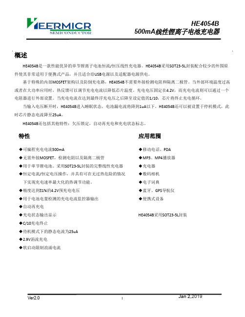
概述HE4054B是一款性能优异的单节锂离子电池恒流/恒压线性充电器。
HE4054B采用SOT23-5L封装配合较少的外围原件使其非常适用于便携式产品,并且适合给USB电源以及适配器电源供电。
基于特殊的内部MOSFET架构以及防倒充电路,HE4054B不需要外接检测电阻和隔离二极管。
当外部环境温度过高或者在大功率应用时,热反馈可以调节充电电流以降低芯片温度。
充电电压固定在4.2V,而充电电流则可以通过一个电阻器进行外部设置。
当充电电流在达到最终浮充电压之后降至设定值的1/10,芯片将终止充电循环。
当输入电压断开时,HE4054B进入睡眠状态,电池漏电流将降到1uA以下。
HE4054B还可以被设置于停机模式,此时芯片静态电流降至25uA。
HE4054B还包括其他特性:欠压锁定,自动再充电和充电状态标志。
特性◆可编程充电电流500mA◆无需外接MOSFET,检测电阻以及隔离二极管◆用于单节锂电池、采用SOT23-5L封装的完整线性充电器◆恒定电流/恒定电压操作,并具有可在无过热危险的情况下实现充电速率最大化的热调节功能。
◆精度达到±1%的4.2V预充电电压◆用于电池电量检测的充电电流监控器输出◆自动再充电◆充电状态输出显示◆C/10充电终止◆待机模式下的静态电流为25uA◆2.9V涓流充电◆软启动限制浪涌电流应用范围◆移动电话、PDA◆MP3、MP4播放器◆充电器◆数码相机◆电子词典◆蓝牙、GPS导航仪◆便携式设备HE4054B采用SOT23-5L封装典型应用打标说明及管脚分布SOT23-5L管脚图丝印字符丝印字符说明左示意图LTH7芯片代码 Y 年号 W 周号 XXXX生产批号管脚描述LTH7YWXXXX最大额定值(注)ESD与Latch-up等级结构框图(如果没有特殊说明,环境温度= 25︒C,输入电压=5V)注释(1): 这时处于充电状态,I CC= I VCC- I BAT(2): 这里C/10终止电流门限指的是终止电流与恒流充电电流的比值使用说明HE4054B是一款专门为锂离子电池设计的线性充电器,利用芯片内部的功率MOSFET对电池进行恒流/恒压充电。
HE3050F V1.1_CN规格书赫尔半导体HEERMICR
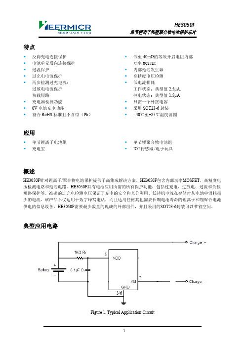
特点•反向充电连接保护•电池单元反向连接保护•过温保护•过充电电流保护•两步检测过充电流:过放电电流保护负载短路•充电器检测功能•0V 电池充电功能•符合RoHS 标准且不含铅(Pb )•低至40mΩ的等效开启电阻内部功率MOSFET •内部延迟发生器•高精度电压检测•低电流损耗工作状态:典型值2.5µA.掉电状态:典型值1.5µA •只需一个外接电容•采用SOT23-6封装•-40℃至+85℃温度范围应用•单节锂离子电池组•充电宝•单节锂聚合物电池组•IOT 传感器/电子玩具概述HE 3050F 针对锂离子/聚合物电池保护提供了高集成解决方案。
HE 3050F 包含内部功率MOSFET ,高精度电压检测电路和延迟电路。
HE 3050F 具有电池应用所需的所有保护功能,包括过充电、过放电、过流和负载短路保护等。
准确的过充电检测电压保证了充电的安全和充分利用。
低待机电流在存储时从电池中消耗很少的电流。
该产品不仅适用于数字蜂窝电话,而且适用任何其他需要长期电池寿命的锂离子和锂聚合电池供电的信息设备。
HE 3050F 需要最少数量的现成的外部组件,并且采用的SOT23-6封装可以节省空间。
典型应用电路Figure 1.Typical Application Circuit523/6HE 3050F单节锂离子和锂聚合物电池保护芯片引脚描述管脚设置Figure 2.Pin Configuration引脚描述引脚名称功能1NC NC2VM连接电池组的负极。
内部FET 开关将这个端口连接到GND 3/6GND 接地引脚5VDD 电源引脚4NCNC印章说明标记描述封装最小包装3代表过放电流值;50代表导通内阻;F 代表SOT-23封装;B 代表过充电压;9代表生产年份;A 代表生产周数SOT23-63000PCS订购须知型号HE 3050F-AHE 3050F-BHE3050F-CHE 3050F-D过充电压 4.250V 4.300V 4.425V 4.475V 丝印图350FA350FB350FC350FD-6HE 3050F单节锂离子和锂聚合物电池保护芯片绝对最大额定值(1)(2)VDD输入电压…………….........…...-0.3V to6V 工作温度范围……………….…...-40°C to+85°C 铅温度(钎焊,10s)…………………..+300°C θJA…….………………….…………........250°C/W θJC……….……...……………...…..........130°C/W VM输入电压…..…………………......…...-6V to10V存储温度范围.....................................-55°C to150°C 结温...........................................................+125°C ESD(Human Body Made)HMB............................2KV ESD(Machine Made)MM (200V)备注1:超过这些额定值可能会损坏器件。
HE4056B电源管理芯片充电管理赫尔微半导体
HE40561.1A Lithium Ion Battery Linear ChargerFeatures●Protection of battery cell reverse connection●Programmable charge current up to 1.1A●No MOSFET sense resistor or blocking dioderequired●Complete linear Charger for single Cell Lithium-IonBatteries●CC and CV operation with thermal regulation tomaximize Rate without risk of overheating●Preset 4.2V charge voltage with ±1% accuracy ●Automatic Recharge●Two Status Indication for Charge status, no batteryand battery failure indicators●C/10 charge termination●55μA supply current in shutdown● 2.9V trickle current charge threshold●Soft-Start limits inrush current●Battery Temperature Sensing●Available in SOP-8 and ESOP-8 packageApplications●Cellular Telephones ●Mobile Power Supply ●Digital Still Cameras ●MP3 Players ●Bluetooth Applications●Portable Devices●USB Bus-Powered ChargersGENERAL DESCRIPTIONHE4056 is a complete CC/CV linear charger for single cell lithium-ion batteries. it is specifically designed to work within USB power Specifications.No external sense resistor is needed and no blocking diode is required due to the internal P-MOSFET architecture.Thermal feedback regulates the charge current to limit the die temperature during high power operation or high ambient temperature .The charge voltage is fixed at 4.2V,and the charge current can be programmed externally with a single resistor. The HE4056 automatically terminates the charge cycle when the charge current drops to 1/10th the programmed value after the final float voltage is reached.When the input supply (wall adapter or USB supply) is removed the HE4056 automatically enters a low current state dropping the battery drain current to less than2μ A.The HE4056 can be put into shutdown mode reducing the supply current to 55μA.Other features include Battery temperature monitor, under-voltage lockout, automatic recharge and two status pins to indicate charge and charge termination.1.1A Lithium Ion Battery Linear Charger Pin Configuration1.1A Lithium Ion Battery Linear ChargerAbsolute Maximum Ratings1.1A Lithium Ion Battery Linear ChargerCaution: The absolute maximum ratings are rated values exceeding which the product could suffer physical damage. These values must therefore not be exceeded under any conditions.1.1A Lithium Ion Battery Linear ChargerNote: The ●denotes specifications which apply over the full operating temperature rang, otherwise specifications are at TA=25℃,VCC=5V,unless otherwise specified.Description of the PrincipleThe HE4056 is a complete CC/CV linear charger for single cell lithium-ion batteries. CC/CV to charger batter by internal MOSFET .It can deliver up to 1.1A of charge current .No blocking diode or external current sense resistor is required. HE4056 include two Open-Drain charge status Pins: Charge status indicator CHRG and battery failure status output STDBY.The internal thermal regulation circuit reduces the programmed charge current if the die temperature attempts to rise1.1A Lithium Ion Battery Linear Chargerabove a preset value of approximately 145℃. This feature protects the HE4056 from excessive temperature, and allows the user to push the limits of the power handling capability of a given circuit board without risk of damaging the HE4056 or the external components. Another benefit of adopting thermal regulation is that charge current can be set according to typical, not worst-case, ambient temperatures for a given application with the assurance that the charger will automatically reduce the current in worst-case conditions.The charge cycle begins when the voltage at the VCC pin rises above the UVLO level, a current set resistor is connected from the PROG pin to ground, and the CE pin is pulled above the chip enable threshold.The CHRG pin outputs a logic low to indicate that the charge cycle is on going. At the beginning of the charge cycle, if the battery voltage is below 2.9V, the charge is in precharge mode to bring the cell voltage up to a safe level for charging. The charger goes into the fast charge CC mode once the voltage on the BAT pin rises above 2.9 V. In CC mode, the charge current is set by RPROG. When the battery approaches the regulation voltage 4.2V, the charge current begins to decrease as the HE4056 enters the CV mode. When the current drops to charge termination threshold, the charge cycle is terminated, and CHRG pin assumes a high impedance state to indicate that the charge cycle is terminated and STDBY pin is pulled low.The charge termination threshold is 10% of the current in CC mode. To restart the charge cycle, remove the input voltage and reapply it, or momentarily force CE pin to 0V. The charge cycle can also be automatically restarted if the BAT pin voltage falls below the recharge threshold. The on-chip reference voltage, error amplifier and the resistor divider provide regulation voltage with 1% accuracy which can meet the requirement of lithium-ion and lithium polymer batteries. When the input voltage is not present, or input voltage is below VBAT, the charger goes into a sleep mode, dropping battery drain current to less than 3μA. This greatly reduces the current drain on the battery and increases the standby time. The charger can be shutdown by forcing the CE pin to GND.The charging profile is shown in the following figure:1.1A Lithium Ion Battery Linear ChargerThe charge current is programmed using a single resistor from the PROG pin to ground. The program resistor and the charge current are calculated using the following equations.BATPROG I R 1450; In application, according the charge current to determine RPROG ,the relation between RPROG and charge current can reference the following chart:Charge TerminationA charge cycle is terminated when the charge current falls to 1/10th the programmed value after the final float voltage is reached. This condition is detected by using an internal filtered comparator to monitor the PROG pin. When the PROG pin voltage falls below 100mV for longer than tTEMP (typically 1.8mS), Charging is terminated. The charge current is latched off and the HE4056 enters standby mode, where the input supply current drops to 55μA ( Note:C/10 termination is disabled in trickle charging and thermal limiting modes).When charging, transient loads on the BAT pin can cause the PROG pin to fall below 100mV for short periods of timebefore the DC charge current has dropped to 1/10th the programmed value. The 1.8mS filter time (tTEMP) on the termination comparator ensures that transient loads of this nature do not result in premature charge cycle termination. Once the average charge current drops below 1/10th the programmed value, the HE4056 terminated the charge cycle and ceases to provide any current through the BAT pin. In this state all loads on the BAT pin must be supplied by the battery. The HE4056 constantly monitors the BAT pin voltage in standby mode. If this voltage drops below the 4.10V recharge threshold (VRECHRG ),another charge cycle begins and current is once again supplied to the battery. To manually restart a charge cycle when in standby mode, the input voltage must be removed and reapplied or the charger must be shut down and restarted using the PROG pin. Figure 1 shows the state diagram of a typical charge cycle1.1A Lithium Ion Battery Linear ChargerThermal limiting1.1A Lithium Ion Battery Linear ChargerAn internal thermal feedback loop reduces the programmed charge current if the die temperature attempts to rise above a preset value of approximately 145℃ . The feature protects the HE4056 from excessive temperature and allows the user to push the limits of the power handling capability of a given circuit board without risk of damaging the HE4056. The charge current can be set according to typical (not worst-case) ambient temperature with the assurance that the charger will automatically reduce the current in worst-case conditions.To prevent the damage caused by the very high or very low temperature done to the battery pack, the HE4056 continuously senses battery pack temperature by measuring the voltage at TEMP pin determined by the voltage divider circuit and the battery ’s internal NTC thermistor as shown in Figure 1.The HE4056 compares the voltage at TEMP pin (VTEMP) against its internal VLOW and VHIGH thresholds to determine if charging is allowed. In HE4056, VLOW is fixed at (45%×Vcc), while VHIGH is fixed at (80%×Vcc). If VTEMP<VLOW or VTEMP>VHIGH , it indicates that the battery temperature is too high or too low and the charge cycle is suspended. When VTEMP is between VLOW and VHIGH , charge cycle resumes. The battery temperature sense function can be disabled by connecting TEMP pin to GND.Under Voltage lockout (UVLO)An internal under voltage lockout circuit monitors the input voltage and keeps the charger in shutdown mode until VCC rises above the under voltage lockout threshold . If the UVLO comparator is tripped, the charger will not come out of shutdown mode until VCC rises 140mV above the battery voltage.Auto restartOnce charge is been terminated, HE4056 immediately use a 1.8ms filter time ( tRECHARGE )on the termination comparator to constant monitor the voltage on BAT pin. If this voltage drops below the 4.1V recharge threshold (about between 80% and 90% of VCC), another charge cycle begins. This ensured the battery maintained (or approach) to a charge full status andavoid the requirement of restarting the periodic charging cycle. In the recharge cycle, CHRG pin enters a pulled down status.Stability ConsiderationsIn CC mode, the PROG pin is in the feedback loop, not the battery. The CC mode stability is affected by the impedance at the PROG pin. With no additional capacitance on the PROG pin, the charger is stable with program resistor values as high as 20K. However, additional capacitance on this node reduces the maximum allowed program resistor. Therefore, if IPROG pin is loaded with a capacitance C, the following equation should be used to calculate the maximum resistance value for RPROG : PROGPROGC R ⨯⨯≤51021πAs user, may think charge current is important, not instantaneous current. For example, to run a low current mode switch power which parallel connected with battery, the average current from BAT pin usually importance to instantaneous current. In this case, In order to measure average charge current or isolate capacitive load from IPROG pin, a simple RC filter can be used on PROG pin as shown in Figure 2. In order to ensure the stability add a 10K resistor between PROG pin and filter capacitor.1.1A Lithium Ion Battery Linear ChargerFig.2 Isolating with capacitive load on PROG PinPower DissipationThe conditions that cause the HE4056 to reduce charge current through thermal feedback can be approximated by considering the power dissipated in the IC. Nearly all of this power dissipation is generated by the internal MOSFET-this is calculated to be approximately:BAT BAT CC D I V V P ⨯-=)(The approximate ambient temperature at which the thermal feedback begins to protect the ICis:JA D A P C T θ⨯-︒=145;So:JABAT BAT CC A I V V C T θ⨯⨯--︒=)(145For example: The HE4056 with 5V supply voltage through programmable provides full limiting current 850mA to a charge lithium-ion battery with 3.85V voltage. If JA is 100℃/W ( reference to PCB layout considerations), When HE4056 begins to decrease the charge current, the ambient temperature about:CT A ︒=⨯⨯--=25.4710085.0)85.35(145HE4056 can work in the condition of the temperature is above 47.25℃, but the charge current will pull down to below 850mA. In a fixed ambient temperature, the charge current is calculated to be approximately :JABAT CC ABAT)V (V T C I θ⨯--=︒145Just as Description of the Principle part talks about so, the current on PROG pin will reduce in proportion to the reduced charge current through thermal feedback. In HE4056 design applications don ’t need to considerate the worst case of thermal condition, this point is importance, because if the junction temperature up to 145℃ ,HE4056 will auto reduce the power dissipation.Thermal ConsiderationsBecause of the small size of the thin SOP-8 or ESOP-8 package, it is important to use a good thermal PC board layout to maximize the available charge current. The PC board copper is the heat sink. The footprint copper pads should be as wide as possible and expand out to larger copper areas to spread and dissipate the heat to the surrounding ambient. Other heat sources on the board, not related to the charger, must also be considered when designing a PC board layout because they will affect overall temperature rise and the maximum charge current.VCC bypass capacitorMany types of capacitors can be used for input bypassing, however, caution must be exercised when using multilayer ceramic capacitors. Because of the self-resonant and high Q characteristics of some types of ceramic capacitors, high voltage transients can be generated under some start-up conditions, such as connecting the charger input to a live powerHE40561.1A Lithium Ion Battery Linear Chargersource. Adding a 1.5Ω resistor in series with a ceramic capacitor will minimize start-up voltage transients.Charging Current Soft StartHE4056 includes a soft start circuit which used to maximize to reduce the surge current in the begging of charge cycle. When restart a new charge cycle, the charging current ramps up from 0 to the full charging current within 20μs. In the start process it can maximize to reduce the action which caused by surge current load.Board Layout ConsiderationsRPROG at PROG pin should be as close to HE4056 as possible, also the parasitic capacitance at PROG pin should be kept as small as possible.The capacitance at VCC pin and BAT pin should be as close to HE4056 as possible.During charging, HE4056’s temperature may be high, the NTC thermistor should be placed far enough to HE4056 so that the thermistor can reflect the battery ’s temperature correctly.It is very important to use a good thermal PC board layout to maximize charging current. The thermal path for the heat generated by the IC is from the die to the copper lead frame through the package lead (especially the ground lead) to the PC board copper, the PC board copper is the heat sink. The footprint copper pads should be as wide as possible and expand out to larger copper areas to spread and dissipate the heat to the surrounding ambient. Feed through vias to inner or backside copper layers are also useful in improving the overall thermal performance of the charger. Other heat sources on the board, not related to the charger, must also be considered when designing a PC board layout because they will affect overall temperature rise and the maximum charge current.The ability to deliver maximum charge current under all conditions require that the exposed metal pad on the back side of the HE4056 package be soldered to the PC board ground. Failure to make the thermal contact between the exposed pad on the backside of the package and the copper board will result in larger thermal resistance.Add thermal regulation currentIt will effective to decrease the power dissipation through reduce the voltage of both ends of the inner MOSFET. In the thermal regulation, this action of transporting current to battery will raise. One of the measure is through an external component(as a resistor or diode) to consume some power dissipation.For example: The HE4056 with 5V supply voltage through programmable provides full limiting current 1000mA to a charge lithium-ion battery with 3.8V voltage. If JA is 120℃/W, so that at 25℃ ambient temperature, the charge current is calculated to be approximately :JABAT CC BAT CC BAT)V R I V CC I θ⨯-⨯--=︒︒(25145In order to increase the thermal regulation charge current, can decrease the power dissipation of the IC through reducing the voltage (as show fig.3) of both two ends of the resistor which connecting in series with a 5V AC adapter.With square equation to calculate I BAT :CCJAA CC BAT CC BAT CC BAT R T C R V V V V I 2)145(4)(2θ-︒⨯----=If RCC=0.25Ω, VCC=5V, VBAT=3.75V, TA=25℃ and JA =120℃/W, we can calculate the thermal regulation charge current: IBAT =1080mA. It means that in this structure it can output 1000mA full limiting charge current at more high ambient temperature environment.Although it can transport more energy and reduce the charge time in this application, but actually spread charge time, if1.1A Lithium Ion Battery Linear ChargerHE4056 stay in under-voltage state, when VCC becomes too low in voltage mode. Fig.4 shows how the voltage reduced with increase RCC value in this circuit. This technique will act the best function when in order to maintain the minimize thedimension of the components and avoid voltage decreased to minimize RCC .USB and Wall Adapter PowerHE4056 allows charging from a USB port, a wall adapter can also be used to charge Li-Ion/Li-polymer batteries. Figure 5 shows an example of how to combine wall adapter and USB power inputs. A P-channel MOSFET, Q1, is used to prevent back conducting into the USB port when a wall adapter is present and Schottky diode, D1, is used to prevent USB power loss through the 1K Ω pull-down resistor.Generally, AC adaptor is able to provide bigger much current than the value of specific current limiting which is 500mA for USB port. So can rise charge current to 600mA with using a N-MOSFET (Q1) and an additional set resistor value as highas 10K.HE40561.1A Lithium Ion Battery Linear ChargerHE4056 has two open-drain status indicator output CHRG and STDBY .CHRG is pull-down when the HE4056 in a charge cycle. In other status CHRG in high impedance,CHRG and are all in high impedance when the battery out of the normal temperature.Represent in failure state, when TEMP pin in typical connecting, or the charger with no battery: red LED and green LED all don ’t light. The battery temperature sense function is disabled by connecting TEMP pin to GND. If battery is not connected to charger,CHRG pin outputs a PWM level to indicate no battery. If BAT pin connects a 10μF capacitor, the frequency of CHRG flicker about 1-4S, If not use status indicator should set status indicator output connected to GND.The values of R1 and R2 in the application circuit can be determined according to the assumed temperature monitor range and thermistor ’s values. The Follows is an example: Assume temperature monitor range is TL ~TH ,(TL <TH);the thermistor in battery has negative temperature coefficient (NTC ),RTL is thermistor ’s resistance at TL , RTH is the resistance atTH ,so RTL >RTH ,then at temperature TL, the voltage at TEMP pin is:INTHTHTEMPH V R R R R R V ⨯+=////212At temperature TH, the voltage at TEMP pin is:INTLTLTEMPL V R R R R R V ⨯+=////212We know VTEMPL =VHIGH =K2×Vcc (K2=0.8);VTEMPH =VLOW =K1×Vcc (K1=0.45) Then we can have :12121)()(K K R R K K R R R TH TL TH TL ⨯--⨯=;)()()(212211121K K K R K K K R K K R R R TH TL TH TL ⨯--⨯--⨯=Likewise, for positive temperature coefficient thermistor in battery, we have RTH >RTL and we can calculate:12121)()(K K R R K K R R R TL TH TH TL ⨯--⨯=;)()()(212211121K K K R K K K R K K R R R TL TH TH TL ⨯--⨯--⨯=We can conclude that temperature monitor range is independent of power supply voltage VCC and it only depends on R1, R2, RTL and RTH: The values of RTH and RTL can be found in related battery handbook or deduced from testing data. In actual application, if only one terminal temperature is concerned (normally protecting overheating), there is no need to use R2 but R1. It becomes very simple to calculate R1 in this case.Block Diagram1.1A Lithium Ion Battery Linear Charger1.1A Lithium Ion Battery Linear ChargerC210uF1.1A Lithium Ion Battery Linear ChargerPackaging Information:SOP8 PACKAGE OUTLINE DIMENSIONS。
HE-480C 半导体清洁过程中的导电度计说明书

Mass
Approx. 400g
Conforming standards
CE Marking, FCC Part15
Compatible sensor
ESH –series conductivity GC sensor, cell constant : 0.1/cm
(Sensor)
Model
ESH-01-L-GC5 ESH-01-L-GC6
For Semiconductor Cleaning Processes
Conductivity Meter Low Concentration Type
HE-480C
Perfect for Chemical Solution Measurement and Recycle of Pure Water in Semiconductor Wet Processes
Measurement method
2-electrode method
Sensor input
1-channel
Cell constant
Approx. 0.1/cm
Temperature sensor specifications Platinum resistance 1000Њ/0ˆ
Mnction
Conductivity : Based on the specified compensation coefficient for the cell constant
(parameter input)
Temperature : Calibrated by comparing with the reference thermometer
Power supply
- 1、下载文档前请自行甄别文档内容的完整性,平台不提供额外的编辑、内容补充、找答案等附加服务。
- 2、"仅部分预览"的文档,不可在线预览部分如存在完整性等问题,可反馈申请退款(可完整预览的文档不适用该条件!)。
- 3、如文档侵犯您的权益,请联系客服反馈,我们会尽快为您处理(人工客服工作时间:9:00-18:30)。
■ 产品概述
HE1160 是一款单节锂电池电量指示芯片,该芯片采用 CMOS 工艺实现,体积小,便于便携式产品安装。
HE1160 内置比较器和反馈回路,实现4 个电压点的检 测。 通过内部修调技术,可以保证电压检测精度达到 ±1%。输出采用OPENDRAIN 结构,便于客户使用IO 口 或者 LED 指示。
2
■ 典型应用电路
■ 电学特性参数
参数 输入电压 静态工作电流 VD4 上升沿检测点 VD4 下降沿检测点 VD3 上升沿检测点 VD3 下降沿检测点 VD2 上升沿检测点 VD2 下降沿检测点 VD1 上升沿检测点 VD1 下降沿检测点 VDX 端口源电流
■ 电量示意表
S1
330
1uF
vdd D1 D2 D3
最低 典型 最高 Unit
2
6.5
V
5
8
10
uA
- 3.87
-
-
3.8
-
3.7
-
- 3.64
-
V
- 3.55
-
- 3.50
-
-
3.4
-
-
3.1ห้องสมุดไป่ตู้
-
5
mA
电压范围(上升)(V) 3.87-4.2 3.7-3.87 3.55-3.7 3.4-3.55 3.4 以下
VD1 VD2 VD3 VD4 亮亮亮亮 亮亮亮灭 亮亮灭灭 亮灭灭灭 灭灭灭灭
GND
功能框图
■ 绝对最大额定值
参数
标号
最大额定值
单位
输入电压
Vcc
VSS-0.3~VSS+7
V
D1-D4 耐压
VD1-VD4
VSS-0.3~Vcc+0.3
V
D1-D4 输出电流
ID1-ID4
30
mA
注意: 绝对最大额定值是指在任何条件下都不能超过的额定值。万一超过此额定值,有可能造成产品劣化等物理性损伤。
■ 产品特点
超低功耗:<10uA 内置 4 路比较器,实现 4 个电压点检测 内部比较器具有合理的迟滞,便于做充放电指示。 高精度:±2%
■ 用途
移动电源
LED 手电 便携式电子设备
■ 封装
SOT23-6L
D1 D2 D3
6
5
4
1
2
3
VDD GND D4
■ 引脚功能
VDD(引脚 1):电源 GND(引脚 2):接地端 D1-D4(引脚 3-6):LED1-LED4 输出指示,D1 为低压端指示,D4 为高压端指示!
3
■ 封装尺寸
SOT23-6L
HE1160
4
gnd D4
HE1160
标号 Vcc ISS VD4R VD4D VD3R VD3D VD2R VD2D VD1R VD1D IDX
条件
VCC=4.5V VCC 上升 VCC 下降 VCC 上升 VCC 下降 VCC 上升 VCC 下降 VCC 上升 VCC 下降 VDD-VDX=0.3V
(Ta=25℃,除非特殊指定)
■ 打印信息
D1 D2 D3
6
5
4
1
2
VDD GND
① 工艺编号
打印符号 A
另注:生产品批号按公司内部固定进行。
3 D4
描述 01A
1
■ 订购信息
HE1160 ①② 标号 ①
②
HE1160
描述 封装类型
器件方向
标记
描述
M
SOT23-6L
R
正面
L
反面
■ 功能框图
VDD
D4 D3 D2 D1 1.2V