Allegro16.5教程 实用学习笔记
Cadenceallegro16.5使用技巧问题总结

Cadenceallegro16.5使用技巧问题总结1.ALLEGRO 自动布线后,为直角调整成45度角走线:Route-Gloss-Parameters-Convert corner to arc。
2.ALLEGRO系统菜单字体太小修改:Setup-User Preferences Editor-Ui-Fonts-fontsize中Value改大点,默认12改为14就差不多了。
3.隐藏覆铜:Setup-User Preferences Editor-Display-shape_fill-no_shape_fill打钩。
覆铜设置Shape-Global Dynamic Parameters.动态填充方式:Smooth、Rough、Disable ,Smooth完全显示避让效果,Rough:铜皮避让显示不完全, Disabled:不显示铜皮避让效果。
覆铜时可以先采用后两种,可以加快布线及DRC检查的速度,但是出Artwork时,通过Update to Smooth转换成过来。
动态铜皮的避让间距Clearances-Thru pin-Oversize value加10mil其他默认。
合并两块铜皮:Shape-Merge Shapes然后分别点击这两块铜皮。
4.添加测试点:Manufacture-Testprep-Automatic进行设置。
5.allegro布线完成后,对一些要进行修改调整Route-Slide,有三种模式可以选择。
6.撤销已经放置好的元件,框选元件右键Unplace component。
7. 在摆放元件时为方便需要关闭飞线:Display–Blank Rats–All 。
8.查找某一元件,Find对话框-Find By Name-Symbol(or Pin)-name输入元件名,Enter.9.约束规则设定:Setup-Constraints-Constraint Manager进行设置。
CadenceAllegro16.5培训教程
CadenceAllegro16.5培训教程Cadence Allegro 16.5培训教程引言Cadence Allegro 16.5是一款功能强大的电子设计自动化工具,广泛应用于电子设计领域。
本文档旨在提供有关Cadence Allegro 16.5培训教程的详细信息,帮助初学者快速上手使用该工具。
第一部分:介绍1.1 Cadence Allegro 16.5概述Cadence Allegro是一款专业的PCB设计工具,提供从原理图设计到布局绘制和印制板制造的全面工作流程。
它具有强大的功能和灵活的工作环境,能够满足各类电子产品的设计需求。
1.2 Cadence Allegro 16.5的优点- 强大的功能:Cadence Allegro 16.5提供了丰富的设计工具,包括原理图绘制、版图设计、信号完整性分析等,能够满足复杂电路设计的需求。
-多种设计约束:Cadence Allegro 16.5支持多种设计约束设置,如电气约束、尺寸约束、信号完整性约束等,保证设计的可靠性和稳定性。
- 高度集成:Cadence Allegro 16.5与其他Cadence软件工具的无缝集成,如OrCAD、Allegro PCB SI等,方便设计师实现整个设计流程的协同工作。
- 内置验证机制:Cadence Allegro 16.5提供了强大的验证工具,如设计规则检查、布局识别检查等,帮助设计师快速发现和解决问题。
- 全面的制造支持:Cadence Allegro 16.5支持从布局到印制板制造的全面工作流程,包括设计生成、工艺规划、生产输出等,保证设计的可制造性和可靠性。
第二部分:基础知识2.1 Cadence Allegro 16.5界面介绍Cadence Allegro 16.5的界面由主窗口、菜单栏、工具栏、设计文件预览等组成。
本节介绍各个组件的功能和使用方法。
2.2 常用命令本节介绍Cadence Allegro 16.5中一些常用命令的使用方法,如绘制元件、连接电路、设置约束等。
allegro16.5中文学习教程

- EDA中国
图 1.2 Pad Designer Layers 界面
如果制作的是表贴元件的焊盘将Single layer mode 复选框勾上。需要填写的参数有: BEGINLAYER 层的Regular Pad;SOLDEMASK_TOP 层的Regular Pad;PASTEMASK_TOP 层的Regular Pad 。如图 1.3 所示。
Allegro 16.5中文教材
目录
第1 章 焊盘制作.........................................................................................................1
1.1 用Pad Designer 制作焊盘........................................................................................... 1 1.2 制作圆形热风焊盘....................................................................................................... 6
电话:021-54311536
元件焊盘设置
国 如果是通孔焊盘,需要填写的参数有:
BEGINLAYER 层的Regular Pad,Thermal Relief,Anti Pad;
4.3.1手工拉线.........................................................................................................56
Allegro16.5原理图与PCB新功能介绍
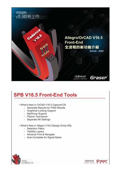
Allegro/OrCAD V16.5Front-EndБ߹۞າΑਕ̬Graser -AddiSPB V16.5 Front-End Tools•What’s New in OrCAD V16.5 Capture/CIS-Generate Reports for FIND Results-Graphical Locking Support-NetGroup Support-PSpice Test-bench-Separate INI Settings•What’s New in Allegro V16.5 Design Entry-HDL-Selection Filters-Visibility Layers-Advance Find & Navigate-Auto-Complete for Signal Name-Generate Reports for FIND Results : Part Search•After you executethe Find commandon a design, youcan generate areport (CSV orHTML) for theresults from thecommand. What’s New in OrCAD V16.5 Capture/CIS-Generate Reports for FIND Results : Net Search-Graphical Locking Support•Lock / Unlock Components from any graphical move–By selection–By page–By designWhat’s New in OrCAD V16.5 Capture/CIS-NetGroup SupportGROUPA[0..31]GROUPA.A[0..7]GROUPA.B[0..7]GROUPA.C[0..7]GROUPA.D[0..7]GROUPA[0..31]NetGroup-PSpice Test-bench•Ability to generate test-benchdesign and inherit simulationprofile from master•Ability to activate portion of test-bench by–Selection in Master–Selection in Project–Selection in Test-bench•Ability to auto-identify floating nets•SVS for updating Master withchanges in TBWhat’s New in OrCAD V16.5 Capture/CIS -PSpice Test-bench•Extract a portion of design into new design for simulation•ECO between Master and Test-bench design-Separate INI Settings•While the Capture INI settings are always dynamic, the CIS settings are more or less static and usually do not change after the initial CIS database related setup.•To allow change in Capture INI settings without affecting CIS settings•16.5 now retains the CIS INI settings in a separate back-up file.These settings are then restored during re-initialization of Capture INIWhat’s New in Allegro V16.5 Design Entry-HDL -Selection Filters-Visibility LayersWhat’s New in Allegro V16.5 Design Entry-HDL -Advance Find & Navigate•Define Objects for Search–Components, Nets, Properties, Notes, Images,Pins, Plumbing Bodies–Current Page, Design or Current–Search String stored for reuse–Wildcard Support•Selection area on Schematic–Search Method•Docking Window–Windows Standard Columns to show information–Filter results–Double click on object to navigate to it–Copy the display data and paste in ExcelAuto-Complete for Signal NameGraser -JonathanAllegro/OrCAD V16.5Back-EndБ߹۞າΑਕ̬TopicUser Interface¾Status Bar Updates¾Highlighting with Stipples ¾3-D Viewer Update ¾Color View UpdateUsability Enhancements¾Group Route Via Patterns ¾Differential Pair Phase Tuning ¾Tapered Traces ¾Snake Breakout¾Stacked Via Enhancements ¾HDI –Tangent Via Update ¾Max Neck Length DRC Update ¾Associative Dimensioning ¾Allegro PDF PublisherTopicDFM¾DFA Enhancement¾Backdrill Enhancement¾New Short Detection ReportIDX FlowEmbedded Component Design¾Overview¾Front to Back Flow¾Setup & Methodology¾Placement Applications¾Class-Subclass Support¾Global Parameters¾Design Constraints¾Substrate Cavities¾Manufacturing Output¾ReportsTopicSI¾App Mode¾Setup and Audit¾Source Synchronous Analysis Enhancements¾PDN Analysis Abilities¾IR Drop Current Path Display¾3D VisualizationUser InterfaceStatus Bar Updates¾Functional responses for¾Class-subclass¾App modes¾Super filter¾Number of selected objects User InterfaceStatus Bar Updates¾Pick Dialog¾Support Zoom-Center in App ModeOLD Version16.5 VersionHighlighting with Stipples¾Color Dialog is enhanced tosupport 15 stipple patternsAssign color optionsHighlight optionsUser InterfaceHighlighting with Stipples¾Highlighting of FixedNets/Components¾Differentiation of Keepout areasConstraint Manager¾Color swatches adjacent to nets with color overridesUser Interface3-D Viewer Update¾Synchronize with layer visibility changes made in the design canvas ¾This mode is enabled by default.¾In previous releases, the 3-D Viewer would have to be closed and then re-opened upon any visibility changes.Color View Update¾Preserve Flip State Option added¾Saved color files sorted alphabeticallyOLD Version16.5 Version Usability EnhancementsGroup Route Via Patterns¾Available when using¾Interactive Group Route¾Multiline Router¾Options leveraged from Specctra¾Via pattern options¾PerpendicularUsability Enhancements Group Route Via Patterns¾Via pattern options¾Stagger¾Via pattern options¾Diagonal Left¾Diagonal RightUsability Enhancements Group Route Via Patterns¾Via pattern options¾In Taper¾Out Taper¾New Phase Tune CommandUsability Enhancements Differential Pair Phase Tuning¾Parameter options include:¾Bump width and height¾Line or Arc¾Parameter options include:¾Bump width and height¾Line or ArcUsability Enhancements Tapered Traces¾New dynamic fillet option¾Shape based fillet designed to “taper”line width changes along a clineTapered Traces¾Set option in gloss parameter form¾Fillet and Tapered TraceUsability Enhancements Snake Breakout¾Designed for Hex Pattern BGABreakout¾Diff Pair and single route¾User Preference Variable¾Made available in 16.3Stacked Via Enhancements¾B/B Via Label¾New color option to differentiate stacked vias from single B/B via¾Copy/Move Stacked Vias¾Command support for maintaining complete stackUsability EnhancementsHDI –Tangent Via Update¾New option to run on selected clinesOLD Version16.5 VersionMax Neck Length DRC update¾Check will transform segment from based to cumulativeUsability Enhancements Associative Dimensioning¾Dimension lines/text dynamically update when associated objects are moved¾Eliminate the need to “re-dimension”when changes are madeOLD Version16.5 Version¾Dimension lines/text dynamically update when associated objects are moved¾Eliminate the need to “re-dimension”when changes are madeUsability Enhancements Associative Dimensioning¾Dimension lines/text dynamically update when associated objects are moved¾Eliminate the need to “re-dimension”when changes are made¾New Dimension Edit Environment¾New ones introduced¾Align, z-copy, instance parametersUsability EnhancementsAllegro PDF Publisher (option)NonͲfilledComponent RefdesComponent OutlineBoard OutlineFilled¾PDF Output driven by Artwork film records¾Existing color settingsUsability Enhancements Allegro PDF Publisher (option)¾Exported Data¾Components¾Component Refdes( with pin numbers)¾Component Properties¾Nets¾Net Name¾Net Properties¾Test pointsUsability Enhancements Allegro PDF Publisher (option)¾Zoom to SelectionDFA Enhancement¾DFA Table to support 4th spacing entry¾“End to Side”¾New syntax –S:S;E:E;S-E;E-S¾In the example below, A and B must be different spacing values¾Usability improvement¾Easier to place component to minimum spacing (dfa pause = 3)Design for ManufacturabilityDFA Enhancement¾DFA Table to support 4th spacing entry¾“End to Side”¾New syntax –S:S;E:E;S-E;E-S¾In the example below, A and B must be different spacing values¾Usability improvement¾Easier to place component to minimum spacing (dfa pause = 3)Backdrill Enhancement¾Any Layer Backdrilling¾Required on Type I HDI Designs where backdrilling of “Core”vias is required¾Currently backdrilling is permitted from only the top & bottom sides of the PCBDesign for Manufacturability New Short Detection Report¾Status dialog now indicates “NetShorting Errors”¾Net Short report also added tostandard report listECAD/MCAD EDMD 1.2 (IDX)¾EDMD Schema v1.2¾Same features as IDF3.0 w/o Panelization¾Standards managed by ProStep consortium ¾Incremental Format¾Baseline¾Incremental change of baseline¾Collaboration¾Accept, reject, suggest changes¾View change before action¾Add comments about changes¾Corporate Partnership¾Cadence/PTCIDX FlowInitial baseline,Incremental modificationsFinal baseline synchronizationInitial baseline,Incremental modificationsFinal baseline synchronizationIDX FlowInitial baseline,Incremental modificationsFinal baseline synchronizationOverview¾Both Active and Passive components can be embedded ¾Passives¾0402 & 0201¾Resistors 10 to 10Meg Ohm¾Caps up to 100 nF¾Height 4 to 13 mils (100-350um)¾Actives¾Ultrathin (4 to 6 mils)¾ESD protection diodes¾Dies (30-50 IO)Embedded Component Design Setup & Methodology¾Embedded Layer Setup¾Define legal layer(s) to embeddedcomponents on¾Controls direction of component¾Body Up¾Body Down¾Permit layers to be “Protruding”¾Components extend in adjacentlayers¾Define Methodology¾Direct Attach¾Indirect AttachPlacement Applications¾Interactive Placement¾RMB support to drop componentto internal layer(s)¾Pre-selection support¾Hover over component thenuse RMB context sensitivemenu to change layer¾Embedded labels¾Options form support forEmbedded Required andOptionalEmbedded Component Design Placement Applications¾Quickplace Application¾Use to quickly placeembedded components totheir destination layer¾Reduce dependency onmanually droppingcomponents to internal layer¾Enhanced to filter componentswith embedded property¾Board Layer pull downsupports embedded layersConstraint ManagerEmbedded_Placement properties can be applied in CM “Properties”Domain Layer, Status and Attach are read-only fieldsEmbedded Component Design Placement Applications¾DFA Support¾Top side table valuesare used to drivecomponent tocomponent clearancePlacement Applications¾Placement Replication¾Supports embeddedcomponents as part ofreplicated circuitryEmbedded compsEmbedded Component Design Class-Subclass Support¾Enabling the “Body up/down”triggers the relevantdatabase infrastructuresupport¾New Embedded GeometryClass¾Placebounds¾Pastemask¾Assembly¾DisplayGlobal Parameters¾Package Height Buffer¾Define a clearance or buffer whencalculating component heightviolations in a substrate¾Minimum Cavity Gap for Merge¾Define the minimum spacingbetween the edges of a cavity beforea merger takes place¾Placebound to via keepout expansion¾Create a via keepout area based onthe Placebound geometry¾Package to Cavity spacing¾Define the clearance from the edgeof the placebound shape to the cavityoutlineEmbedded Component Design Global Parameters¾Via Connect Height¾Define a height constant for the gapbetween the conductor layer andcomponent pin suspended in thedielectric area¾Default Via Connect Padstack¾Use to define connect point ofcomponent. Typically a single layermicro via.¾Cavity to Route Keepout Expansion¾Become available when a layer is setto “Protruding Allowed”. While thecavity has inherent route keepoutbehavior, it may be desirable toextend the keepout area beyond thecavity profileConstraints¾Package to Cavity¾Define the clearance betweenthe symbol’s place-boundshape to edge of cavity¾Package Height to Layer¾Enable to detect symbolheight violations in dielectricspace¾Integrated Spacing DRCs¾Basic metal to metal¾Embedded SMD pin to viashown in figureEmbedded Component Design Substrate Cavities¾Closed Cavity¾The space around the embedded component in the dielectric between two etch layers. The XY dimensions of the cavity aredriven by the size of the component. In most applications, the cavitywill be between two adjacent layers; however, multilayer cavities issupported.¾Open Cavity¾A blind hole in the substrate in which components are placed. This hole is open to one of the external substrate surfaces and may beseveral layers deep. The cavity may have progressively smallerlengths and widths from the external surface to the depth of thecavity.Manufacturing Output¾Cross Section Chart¾New in 16.5¾Menu Path: Manufacturing–Cross Section Chart¾Drill Legend¾Support of Cavities¾Start:Stop Layer¾Qty of comps¾Artwork Film Records¾ODB++ ver9.1Embedded Component Design Reports¾New Reports¾Embedded Component¾Embedded Cavity¾Updates to Existing Reports¾Component¾Placed Component¾Summary Drawing¾Design Rule ChecksSI App Mode¾Improved integration for board levelsimulation¾Available and Launched like other App Modes ¾No need to switch editors¾Super Command for SI related tasks and includes:Highlight on hover Context sensitive RMB menusSI Setup and Audit¾New commands to replace existing¾Both are Wizard based¾Addresses issues with currenterror / warning pop-ups¾New menu location (Setup)¾Both offer Category & Net selectionSource Synchronous Analysis Enhancements ¾Multi Strobe Support¾(aka Address topology)¾Timing Margin Calculation¾Updated Bus Simulation Report¾Added flexibility for derating tablesPDN Analysis Abilities¾Static IR Drop Analysis¾Voltage drop distribution¾Current distribution¾Current density distribution¾Temperature distribution¾PI Plane Analysis¾Design guide¾Pre-route analysis¾PI Network Analysis¾Post-route verificationIR Drop Current Path Display¾Showing current flowing direction with arrows¾Canvas selection reveals current value in Options paneIR Drop Current Density Display ¾Easy to find “hot spots”¾Current direction shown as well3D Visualization ¾Stretch Item¾Env var: PDNS_3DVIEWER ¾Ability to display¾Impedance (FD)¾Voltage Ripple (TD)¾Current Density (TD)¾Temperature Rise(TD)¾Binary file created (.emv)¾Threshold plane display¾Worse case display¾Layer-based display63。
2-Cadence_Allegro_16.5_PCB操作说明

一、A llegro软件介绍1、启动软件2、软件界面介绍3、工作界面介绍4、命令窗口介绍命令窗口显示所有操作状态以及说明,有时操作无反应,可在命令窗口中查看原因。
也可以在命令窗口输入指令,指令格式(空格做间隔符)如下:定点坐标:x 横坐标纵坐标横向偏移:ix 横向偏移值纵向偏移:iy 纵向偏移值5、Find选择栏介绍Find控制面板用于筛选PCB设计中可选择的元素/对象(Design Object Find Filter)和快速查找元素/对象(Find by Name)。
6、Visibility选择栏介绍控制布线层以及每层中元素/对象的显示。
在设置时可以整体设置,也可以单独设置。
7、Options选择栏介绍这功能是体现Allegro控制操作方便性,用户不用去记忆每个命令的相关参数在哪设置,执行具体命令后Option的相关参数就显示当前命令有关的设置。
二、库路径设置首先将库路径加载进来,导入网表之后,布局时直接调用器件PCB封装进行布局布线。
Setup->User Preferences1、devpath、psmpath对应的库文件在package文件中;2、padpath对应的库文件在pad文件夹中。
三、环境设置1、格点设置:格点的大小确定器件移动每一步的距离。
格点设置小,器件移动更自由。
格点设置大,器件更易自动按格点对齐。
布局阶段,格点可设置大一点,当布局较密集时,格点需设置小点。
Setup->Grids2、页面设置:设置单位制、精度、设计图面的大小、原点坐标Setup->Design Parameters->Design四、导入DXFDXF图中给出了板框图形、板面固定器件的位置、板面禁布区域、板面限高区域,布局之前一定要导入板面DXF图。
File->Import->DXF1、选择DXF所在路径;2、DXF是mm制单位时,此处选择mm,DXF图为mil制,此处选择mil,一般为mm制;3、一般三个选项均选上;4、点一下,再点取消;5、给DXF图在PCB文件中分配所在层a)选中DXF中的所有图层b)设置DXF所在层为BOARDGEOMETRYc)建立新子层d)给新子层取名字,一般为dxf_top、dxf_bot,名字最好能直观。
(精品)Cadence_Allegro_16.5_PCB教程
• 学习要点:
• •
A在llAegllreogL的roe符PsC号Bs介Doe绍snig4ner中创元建件元件封封装装符制号作
种类
注释
Package Symbol(*.psm)
元件封装符号(如,dip14,soic14,R0603,C0805等等。)
Mechanical Symbol(*.bsm)
寸单位和通孔类焊盘的钻孔参数; Layers标签用于设置焊盘各层的信息。
使用Pad Designer创建焊盘
设置钻孔参数
• 设置焊盘各层时,首先鼠标选择需要设置的层,然后在下方设置该层焊盘的形 状和尺寸。
使用Pad Designer创建焊盘
设置焊盘类型 焊盘浏览
定义焊盘形状和尺寸
使用Pad Designer创建焊盘
Mechanical symbol (.bsm)
format symbol
(.osm)
Shape symbol Flash symbol (.ssm)
(.fsm)
Padstacks
元件封装
Assembly Outline
Silk Ref
Assy Ref (mandatory) Device Type
Add->3pt Arc
Add->Line
定义封装边界
• 选择“Add->Line(rectangle)->Package Boundary”定义封装边界
添加元件标识
• 选择“Layout->Lables->RefDes”添加丝印层和装配层的标识。除此之外,还可 以添加device、value、Tolerance等文字信息。
.fsm
加载热风焊盘的库路径
ADSPCB板图仿真学习笔记(过孔设定差分仿真差分眼图仿真等)

ADS PCB 板图仿真学习笔记方法一:1.打开Cadence:Allegro PCB Designer 16.5,载入需要的PCB文件。
1.1File----->Change Editor,在弹出窗口选择Allegro PCB DesignXL(Legacy),选中Analog/RF,点击确定。
1.2Setup----->Cross-section 设置叠层厚度,介电常数等信息。
1.31.3.1RF-PCB----->IFF Interface----->Export,在弹出窗口选择Export Selection,然后点击PCB上需要导出仿真的线段等,点击OK.(也可以选择Export All等其它选项,根据需要选择)。
1.3.2在弹出窗口:RF IFF Export,选择文件存放的路径,然后点击layer map。
1.3.3在出现的窗口选择转换到ADS对应的层(我习惯4层板依次放在PC1~PC4),点击OK。
1.3.4回到RF IFF Export窗口,点击OK,生成文件。
在产生的报告中,Types of viasexported 后给出了过孔输出对应的层。
2打开ADS 20092.1新建一个PCB(可在Option----->Preferences 弹出窗口中选择layout units 设定layout 单位,也可以在layout 界面单机右键,选择Preferences。
另单击右键选择Grid Spaction 可设置栅格大小;选择Measure可用来测量长度)2.2File----->Export 在弹出的Export窗口中,File Type选择IFF;Destination file选择刚才生成的layout.IFF文件(备注:文件夹命名不能有空格等非法字符)。
2.3Momentum----->Substrate----->open 选择刚才生成的xxxx.slm文件,载入叠层设置。
allegro 16.5作电源分割笔记
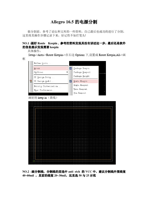
Allegro 16.5的电源分割
做分割前,参考了论坛和文库的一些资料,自己最后也成功的进行了分割,这里将其操作步骤记录下来,好记性不如烂笔头!
NO.1 :画好Route Keepin , 参考的资料发现其没有讲述这一步,最后还是软件的信息提示发现需要keepin
具体操作:
Setup->Area->Route Keepin->在右边Options下,设置成Route Keepin,All->画框
画好的keep in(黄线)
NO.2 :画分割线,分割线的层选中anti etch 的VCC中,建议分割线外围线宽40~60mil ,里面的线宽20~30mil,这里选50与25示范
Add line 开始画分割线
NO.3 :设置分割参数和创建区域Edit -> split plane -> parameters
一般默认solid就可以了
接下来在在Edit -> split plane ->creat,创建区域
接下来在软件的引导下将划分的铜块的网络assign ,注意完成后检查有没有之前漏掉或者过孔过多导致有的过孔没被连接上的情况,下图是执行create后弹出的引导,因为没有网络所以我的dummy net
NO.4 : 所有电源网络assign net 完成后,检查分割是否完整。
- 1、下载文档前请自行甄别文档内容的完整性,平台不提供额外的编辑、内容补充、找答案等附加服务。
- 2、"仅部分预览"的文档,不可在线预览部分如存在完整性等问题,可反馈申请退款(可完整预览的文档不适用该条件!)。
- 3、如文档侵犯您的权益,请联系客服反馈,我们会尽快为您处理(人工客服工作时间:9:00-18:30)。
目录
一、常用操作 (3)
1、Extents选项无法改小 (3)
2、没有自己的Pad (3)
3、命令放入焊盘 (3)
4、命令坐标、增量 (4)
5、表贴元件几个Class、Subclass (4)
6、Create Symbol (4)
7、倒角 (4)
8、设置Keepin (4)
9、设置圆滑连线 (5)
10 z-copy命令 (5)
11 放置元件到Bottm (5)
12 设置带端接的等长line (6)
13 设置差分对 (6)
14 群组走线 (6)
15 区域特殊规则设置 (7)
16 Application Mode切换方便布件走线 (8)
17 对齐摆放元件 (9)
18 光绘层信息 (9)
19 Gerber 钻孔 (10)
20 导出坐标信息 (13)
21 Dimension信息 (13)
二笔记 (15)
2.1导线自感估算 (15)
2.2 PCB板基本外框 (15)
三常见错误解决办法 (16)
3.1 No product licenses found... .. (16)
一、常用操作
1、Extents选项无法改小
Extents选项无法改小时,逐步改小,
如500,400,300.100.50.10.6…可修改
成功。
2、没有自己的Pad
自己画的Pad文件目录没有被识别,放到
原Pad同一目录。
3、命令放入焊
盘
x 0 0回车
格式:x空格0 空格
0 空格
4、命令坐标、增量
x 0 0 表示坐标(0,0)
ix 1.8 表示坐标x方向增量1.8
iy 2 表示坐标y方向增量2。
可用来制定坐标放置元件、制定坐标或增量画线。
5、表贴元件几个Class、Subclass
Stack-Up: Top、Soldermask_Top、Pastemask_Top
Package Geometry: Assembly_Top、Place_Bound_Top、Silkscreen_Top。
6、Create Symbol
Create Symbol 才可以保存成.ssm 文件。
Ssm文件加载到Pad Designer制作焊盘。
制作成ssm后Pad Designer中没有该焊盘需设置Setup User Preferences Editor Paths Library padpath 双击添加ssm文件路径。
7、倒角
Manufacture 》Drafting 》Fillet 弧角,Chamfer 45度角。
依次单击要倒角的两个临边。
使PCB边框直角变为弧角或45度角。
防止划伤其他物品。
8、设置Keepin
Setup 》Area 》Keepin
9、设置圆滑连线
Setup àDesign Parametre Editor àDisplay àConnect Line Endcaps (Allegro PCB 16.5)
Setuo àDrawing Option àDisplay (Allegro PCB 16.2)
10 z-copy命令
用于复制shape到相同或不同的层,支持缩放一定尺寸。
11 放置元件到Bottm
放置或修改Mirro既可以,镜像后即放置到底层。
12 设置带端接的等长line
13 设置差分对
13.1 创建差分对
Electrical à Routing à Wiring 右键选中两个网络后Create Differential Pair。
13.2 设置差分对
Electrical à Routing à Differential Pair。
设置Coupling Parameters
14 群组走线
Add Connection状态下,右键Temp Group –> 逐个单击要群组走线的网络
–>Done -> 移动开始群组走线。
当群组走线时需要单独处理某一条线时,右键单击Single Trace Mode,取消勾选后恢复群组走线。
15 区域特殊规则设置
打开Constraints
建立Region
创建shape Constrain Region、all、rgn1(刚才创建的名字),然后绘制特殊规则区域并关联。
16 Application Mode切换方便布件走线
Allegro 16.5的SetupàApplication Mode中General Edit、Placement Edit、Etch Edit 三种模式分别适用于
普通编辑:几乎所有编辑的操作都是先选择命令在执行对应的动作;
布件编辑:适合摆放元件,方便对齐移动的操作,使操作简单化;
布线编辑:适合布线,布线命令得到简化,方便布线。
17 对齐摆放元件
该命令需要理解上一命令,在Placement Edit模式中,选中要对齐的同一类元件后,在对齐的基准元件上右键àAlign Components。
完成选中元件向选中元件(基准元件)的对齐操作。
18 光绘层信息
Adt/adb装配层
信号层
钻孔层
丝印层
阻焊层
助焊层,也叫钢网信息
19 Gerber 钻孔一般默认即是。
20 导出坐标信息
21 Dimension信息
Allegro支持自动标注尺寸、角度等信息
点击“Dimension Edit”右键选择Linear dimension 或者Angular dimension点击要标注的位置完成距离、角度的标注信息。
或者直接在菜单中找到该菜单
删除Dimension 必须用专用的删除命令,进入Dimension Environment后,右键Delete Dimension。
点击要删除的Dimension。
二笔记
2.1导线自感估算
单位长度导线的自感约为25nH/inch。
例如:0.1inch的导线接头的自感约为2.5nH。
圆形线圈的回路自感近似为:
Lself=32*R* ln(4R/D) nH
Lself表示自感,单位nH;
R表示线圈半径,单位inch;
D表示导线直径,单位inch
例如,由10mil厚的导线绕成半径0.5inch的圆形线圈,则他的回路电感约为85nH。
2.2 PCB板基本外框
PCB板基本外框包含:Route Keepin all(shape),Place Keepin all(shape),Board Geomety/Outline(Line)
三常见错误解决办法
3.1 No product licenses found…
启动时提示:No product licenses found,e-help for list of list of licenses
原因:Serviice 未能有效加载Licence启动。
解决办法:在电脑开始菜单中的程序里找到cadence文件夹,点开再点开License Manager,运行License servers configuration Unilily,弹出的对话框中点browes...指向第7步拷贝到桌面上的license.lic,打开它(open)再点下一步(next),将Host Name项中主机名改成你的电脑系统里的主机名(完整的计算机名称),然后点下一步按界面提示直到完成第7步.。