电路分析第二章习题答案
数字集成电路分析与设计 第二章答案

CHAPTER 2P2.1. a) The solution for the NMOS case is based on Example 2.4: The equation for V T0 is: 02BT FB F OXQ V V C φ=-- Calculate each individual component.1710()1362OX 077200611196310ln 0.026ln 0.44 V 1.4100.440.550.99 V 4 3.510 F/cm1.610 F/cm 310310/0.188 V 1.610610 1.6100.1.610i FpA GC Fp G gate OXB B OX OX OX n kT q NC Q Q C cmC Q C φφφφεε-------⨯==-=-⨯=-=--=-==⨯=⨯⨯=⨯==⨯⨯⨯⨯==⨯TO 06 V V 0.99(0.88)(0.188)0.0600.018 V=------=+ For the PMOS device:1710()77200611196TO 310ln 0.026ln 0.44 V 1.4100.440.550.99 V 310310/0.188 V1.610610 1.6100.06 V 1.610V 0.99(0.88)(0.188)0.0600.138 D Fn i GC Fn G gate B B OX OX OX N kT q n Q Q C cmC Q C φφφφ-----⨯===⨯=-=+=+⨯=⨯==⨯⨯⨯⨯==⨯=---=-Vb) The magnitude of V T0 would be higher. Since the device is PMOS this means that V T0 islowered. Since the only thing that’s been changed is the doping of the gate, only G φ changes. The new V T0 then becomes:00.110.880.1880.6 1.24V T V =----=-c) Since V T0 will be adjusted with implanted charge (Q I ):60.40.0180.382(1.610)(0.382)IOXIOXI Q C Q V C Q V -=-==⨯To calculate the threshold implant level N I :I I I I qN Q Q N q==For the NMOS device from part(a):6122190.610 3.8210/1.610I I Q N ions cm q --⨯=-=-=⨯⨯ (p-type) For the PMOS device from part(a):612219(1.610)(0.40.138)2.6210/1.610I I Q N ions cm q --⨯-=-=-=⨯⨯ (n-type) For the PMOS device from part(b):612219(1.610)(1.240.4)8.410/1.610I I Q N ions cm q --⨯-=-=-=⨯⨯ (p-type)d) The advantage of having the gate doping be n + for NMOS and p + for PMOS could be seen from analysis above. Doping the gates in such a way leads to devices with lower threshold voltages, but enables the implant adjustment with the same kind of impurities that used in the bulk (p-type for NMOS and n-type for PMOS). If we were to use the same kind of doping in gate as in the body (i.e. n + for PMOS and p + for NMOS) that would lead to higher un-implanted threshold voltages. Adjusting them to the required lower threshold voltage would necessitate implantation of the impurities of the opposite type near the oxide-Si interface. This is not desirable. Also, the doping of the poly gate can be carried out at the same time as the source and drain and therefore does not require an extra step.P2.2. First, convert ox t to units of cm:810100cm222210cm 10ox t -=⨯=ÅÅNow, using the mobility equation:()()20 1.8568130/V70cm0.8114102210pep nGS T ox cm V s V V t μμθ--==≈⎛⎫⎛⎫-+ ⎪⎪+ ⎪⎝⎭⎝⎭P2.3. a) For each transistor, derive the region of operation. In our case, for 0V,0.4V GS V =, thetransistor is in the cutoff region and there is no current. For 0.8V,1.2V GS V =, firstcalculate the saturation voltage Dsat V using:()GS T C DSAT GS T C V V E L V V V E L-=-+For our transistors, this would be:Next, we derive the IV characteristics using the linear and saturation current equations,we get the graphs shown below.IV Characteristic of NMOS01020304050607000.20.40.60.811.2Volts (V)C u r r e n t (u A )IV Characteristic of PMOSVolts (V)C u r r e n t (u A )To plot DS I vs. GS V , first identify the region of operation of the transistor. For GS T V V <, the transistor is in the cutoff region, and there is negligible current. For GS T V V > and GS DS V V ≤, the transistor is in the saturation region and saturation current expression should be used. The graphis shown below. Clearly, it is closer to the linear model.Ids vs. Vgs of NMOS010********607000.20.40.60.811.21.4Vgs (V)I d s (V )P2.4. For each transistor, first determine if the transistor is in cutoff by checking to see if V GS isless than or greater than V T . V T may have to be recalculated if the source of the transistor isn’t grounded. If V GS is less than V T , then it is in cutoff, otherwise, it is in either triode or saturation.To determine if it is in the triode saturation region, check to see if V DS is less than or greater than V DSAT . If V DS is less than V DSAT , then it is in triode, otherwise, it is in saturation. a. Cutoff00.200.2V0.4V GS G S T T GS TV V V V V V V =-=-===∴<b. Cutoff01.2 1.20V0.4V GS G S T T GS TV V V V V V V =-=-===∴<c. Linear01.20 1.2V0.4V GS G S T T GS TV V V V V V V =-=-===∴>The transistor is not in the cutoff region.()()()()()()1.20.460.20.48V 1.20.460.20.2V GS T C DSATGS T C DS DS DSATV V E L V V V E L V V V --===-+-+=∴<d. Saturation: In this case, because D G V V > the transistor is in the saturation region. To see this, recognize that in a long-channel transistor if D G V V >, the transistor is in saturation. Since the saturation drain voltage Dsat V is smaller in a velocity-saturated transistor than in a long-channel transistor, if the long-channel saturation region equation produces a saturated transistor, than the velocity-saturated saturation region equation will also.P2.5. In both cases, the first step it to calculate the maximum value of X V given G V . If thevoltage at the drain is higher than this maximum value, then ,max X X V V =, otherwise,X D V V =. The maximum value of X V is G T V V - but 0T T V V ≠ because of body effect andwe consider its effect.(),max 0001.20.40.988X G T G T G T G T V V V V V V V V V γγγγ=-=-+=--=--+=--=-There are two ways to calculate this, either through iteration or through substitution. Iteration:For the iteration method, we need a starting value for V X,max . A good starting value would be 0 1.20.40.8V G T V V -=-=. We plug this value on the RHS of the equation, calculate a new V X,max and repeat until we reach a satisfactory converged value.Old Vx,max New Vx,max 0.800 0.728 0.728 0.734 0.734 0.734In this, only three iterations are needed to reach 0.734V. Substitution:The term makes things a bit tricky, we get around this by making the following substitution:2,max 2,max 0.880.88X X x V V x =+∴=-Therefore:,max 220.9880.880.98800.2 1.87X V x x x =--=-=+-2,max 1.27, 1.470.880.733,1.28X x V x ===-=-= We use the first value since second value is above V DD . a. Since ,max D X V V >, ,max 0.733V X X V V ==. b. Since ,max D X V V <, ,max 0.6V X X V V ==. P2.6.a. Initially, when 0V in V =, the transistor is in the cutoff region and 0V X V =. Thisvalue is constant until V in exceeds V t 0. From then, X in T V V V =- and body effect must be taken into account. This trend continues until 0.7V X D V V ==, and the value of V inat that point must be calculated. From then on, 0.7V X D V V ==. To plot V X in the second region, we first derive an expression for V X vs. V in.(),max 0000.40.212X G T G T in T in T in in V V V V V V V V V V V γγγγ=-=-+=---=--=--=--Substituting:2,max2,max 0.880.88X X x V V x =+∴=-Therefore:,max 220.2120.880.21200.20.66X in in in V V x V x x V =---=--=+--220.880.88XxV x====-=-⎝⎭Since this is a quadratic function, there will be two graphs of V X. Only one of thesegraphs intersects with V X in the first region. In this case, plug 0.4inV= and see which one gives 0V. In our case, it would be the ‘+’ version of the quadratic.To see where region 3 begins, we simply isolate V in:()()()22220.880.2 2.710.2 2.71440.2 2.711.16V4XinVV=-⎝⎭-+-==+-==The final graph is shown in Figure 错误!未找到引用源。
电路分析第二章练习题答案
电路分析第二章练习题答案电路分析是电气工程专业的一门基础课程,通过学习电路分析,可以帮助我们理解和解决电路中的各种问题。
在电路分析的学习过程中,练习题是非常重要的一环,通过解答练习题,可以巩固所学的知识,提高解决问题的能力。
本文将给出电路分析第二章练习题的答案,希望对大家的学习有所帮助。
第一题:根据题目给出的电路图,我们可以看到有一个电阻R1和一个电源V1。
根据欧姆定律,电流I1等于电压V1除以电阻R1,即I1=V1/R1。
第二题:根据题目给出的电路图,我们可以看到有一个电阻R2和一个电源V2。
根据欧姆定律,电流I2等于电压V2除以电阻R2,即I2=V2/R2。
第三题:根据题目给出的电路图,我们可以看到有一个电源V3和两个电阻R3和R4。
根据欧姆定律,电流I3等于电压V3除以电阻R3,即I3=V3/R3。
同样地,电流I4等于电压V3除以电阻R4,即I4=V3/R4。
第四题:根据题目给出的电路图,我们可以看到有一个电源V4和两个电阻R5和R6。
根据欧姆定律,电流I5等于电压V4除以电阻R5,即I5=V4/R5。
同样地,电流I6等于电压V4除以电阻R6,即I6=V4/R6。
第五题:根据题目给出的电路图,我们可以看到有一个电源V5和三个电阻R7、R8和R9。
根据欧姆定律,电流I7等于电压V5除以电阻R7,即I7=V5/R7。
同样地,电流I8等于电压V5除以电阻R8,即I8=V5/R8。
还有电流I9等于电压V5除以电阻R9,即I9=V5/R9。
通过以上的练习题,我们可以看到电路分析中的一些基本概念和计算方法。
在解答这些练习题的过程中,我们需要熟练掌握欧姆定律和串并联电路的计算方法。
同时,我们也需要注意电流的方向和电压的极性,以确保计算的准确性。
电路分析是一门需要理论和实践相结合的学科,通过解答练习题,我们可以将理论知识与实际问题相结合,提高解决问题的能力。
在学习电路分析的过程中,我们还可以借助电路模拟软件进行实验,以加深对电路的理解。
电路原理习题答案第二章电阻电路的等效变换练习
第二章电阻电路的等效变换等效变换”在电路理论中是很重要的概念,电路等效变换的方法是电路问题分析中经常使用的方法。
所谓两个电路是互为等效的,是指(1)两个结构参数不同的电路再端子上有相同的电压、电流关系,因而可以互代换的部分)中的电压、电流和功率。
相代换;(2)代换的效果是不改变外电路(或电路中未由此得出电路等效变换的条件是相互代换的两部分电路具有相同的伏安特性。
等效的对象是外接电路(或电路未变化部分)中的电压、电流和功率。
等效变换的目的是简化电路,方便地求出需要求的结果。
深刻地理解“等效变换” 的思想,熟练掌握“等效变换”的方法在电路分析中是重要的。
2-1 电路如图所示,已知。
若:(1);(2);(3)。
试求以上3 种情况下电压和电流。
解:(1)和为并联,其等效电阻,则总电流分流有2)当,有3),有2-2 电路如图所示,其中电阻、电压源和电流源均为已知,且为正值。
求:(1)电压和电流;(2)若电阻增大,对哪些元件的电压、电流有影响?影响如何?解:(1)对于和来说,其余部分的电路可以用电流源等效代换,如题解图(a)所示。
因此有2)由于和电流源串接支路对其余电路来说可以等效为个电流源,如题解图(b)所示。
因此当增大,对及的电流和端电压都没有影响。
但增大,上的电压增大,将影响电流源两端的电压,因为显然随的增大而增大。
注:任意电路元件与理想电流源串联,均可将其等效为理想电压源,如本题中题解图(a)和(b)o但应该注意等效是对外部电路的等效。
图(a)和图b) 中电流源两端的电压就不等于原电路中电流源两端的电压。
同时,任意电路元件与理想电压源并联,均可将其等效为理想电压源,如本题中对而言,其余部分可以等效为,如题图(c)所示。
但等效是对外部电路(如)的等效,而图(c)中上的电流则不等于原电路的电流。
2-3 电路如图所示。
(1)求;(2)当时,可近似为,此时引起的相对误差为当为的100倍、10 倍时,分别计算此相对误差。
电路分析基础 上海交通大学出版社 习题答案第二章汇总
2.1 解:对节点列KCL 方程,得① 01=i② 032=+i i③ 0643=++i i i④ 6521i i i i =++⑤ 054=+i i对封闭面列KCL 方程,得②③④节点构成的闭合面:0541=++i i i③④⑤节点构成的闭合面:0321=++i i i②③④⑤节点构成的闭合面:01=i2.2 解:00543164218975645632432631521=+++=+-+=-+-=-+-=-++-=++-=++=++u u u u u u u u u u u u u u u u u u u u u u u u u u u2.3 解:对a 节点列KCL 方程,得A I I I I 123221441=-=-=+=对回路1列KVL 方程,得AI I I I I 45018212125062121255154==+++=+++ 对b 、c 、d 、节点列KCL 方程,得AI I I I I I A I I I I I I AI I I I I I 2)3(1143341623263512125546654=---=-==+-=-=-==+-=-=-=+=对回路2列KVL 方程,可求得UV U I I I U 242611236)3(4123646463=⨯-⨯++-⨯=++=+2.4 解:KCL :00521654431=-+-=++-=+-I I I I I I I I IKVL :23143205652643541=-+=++=--I I I I I I I I I2.5 解:利用支路电流法,对电路列出KCL 、KVL 方程,有 KCL :5644326210i i i i i i i i i =++==++KVL :333554411333222244666i R u i R i R i R u i R i R i R i R u i R s s s +=+=+++=+代入已知条件,解得:A i 956.05-=2.6 解:利用支路电流法,对电路列出KCL 、KVL 方程,有KCL : c b e I I I +=KVL :c c e e c ee b be b b b I R U I R U I R I R I R U ++=++=其中 b c I I β=代入已知条件,解方程得:AI A I AI e c b 3351016.11013.11027.2---⨯=⨯=⨯=2.7 解:假设网孔电流的参考方向如下图所示。
工程电路分析第八版第二章答案
Engineering Circuit Analysis
8th Edition
Chapter Two Exercise Solutions
16.
q = i.t = (10-9 A)(60 s) = 60 nC
Copyright ©2012 The McGraw-Hill Companies. Permission required for reproduction or display. All rights reserved.
Chapter Two Exercise Solutions
7.
(a) P = 550 mJ/ 15 ns = 36.67 MW (b) Pavg = (550 mJ/pulse)(100 pulses/s) = 55 J/s = 55 W
Copyright ©2012 The McGraw-Hill Companies. Permission required for reproduction or display. All rights reserved.
Copyright ©2012 The McGraw-Hill Companies. Permission required for reproduction or display. All rights reserved.
Engineering Circuit Analysis
8th Edition
Engineering Circuit Analysis
8th Edition
Chapter Two Exercise Solutions
17.
(a) # electrons = -1013 C/(-1.602×10-19 C/electron) = 6.242×1031 electrons
电工电子学第二章习题答案(2)
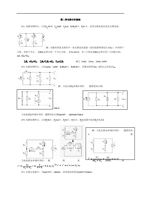
第二章电路分析基础2-1 电路如图所示,已知US1=24V,US2=16V,IS=1A,R1=R2=8Ω,R3=4Ω。
试用支路电流法求各支路电流。
解:该题有四条支路其中一条支路是恒流源(设恒流源两端电压为U IS),应列四个方程。
有两个节点,按KCL定理可列一个节点方程: I1+I2 =I S+I3有三个网孔按KVL定理可列三个回路方程:I1R1 =U S1+U ISI2R2 =U S2+U IS I2R2+I3R3 =U S2 U IS=I3R3 解之 I1=2A I2=1A I3=2A U S=8V2-2 电路如图所示。
已知I S=2A,U S=6V,R1=R2=3Ω,R3=R4=6Ω,用叠加原理求a、b两点之间电压U ab。
解:当电压源U S单独作用时,题图变如右图:Uab1=当电流源I S单独作用时,题图变如右图Uab2=3V Uab=Uab1+Uab2=2-3 电路如图所示。
已知R1=6Ω,R2=12Ω,R3=8Ω,R4=4Ω,R5=1电路中流经R3的电流I当电流源I S单独作用时,题图变如右图)(13844434AIRRRI=⨯+=+=''I=)(211AII=+=''+'2-4 在图示电路中,当U S=24V时,Uab=8v. 试用叠加原理求U S=0时的UabIs。
解:当电压源U S单独作用时,题图变如右图)(1841243ARRUI S=+=+='解:以知U S=24V时,Uab=8v.当U S、、I S1、I S2、单独作用时题图分别变作变作下图1、图2、图3由图1可得:Uab1=)(64244VRRUS-=-=⨯;由图2可得:Uab2=)(212411VRIRRISS=⨯;由图3可得:Uab3=)(41422VRIRISS=⨯;UabIs=Uab2+Uab3=8+6=14(V)2-5 用电源等效变换法求图示电路中6Ω电阻中的电流I。
电工学-第二章习题答案
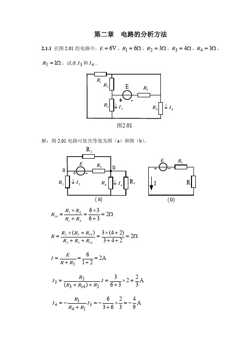
第二章 电路的分析方法2.1.1 在图2.01的电路中,V 6=E ,Ω=61R ,Ω=32R ,Ω=43R ,Ω=34R ,Ω=15R 。
试求3I 和4I 。
4I ↓图2.01解:图2.01电路可依次等效为图(a )和图(b )。
R 3R 1R(b)Ω=+×=+×=23636414114R R R R R Ω=+++×=+++×=2243)24(3)(14321432R R R R R R R A 22165=+=+=R R E IA 322363)(214323=×+=++=I R R R R IA 943263631414−=×+−=+−=I R R R I2.3.3 计算图2.12中的电流3I 。
Ω=1R A2S =图2.12解:根据电压源与电流源的等效变换,图2.12所示电路可依次等效为图(a )和图(b ),由图(b )可求得A 2.15.023=+=I由图(a )可求得:A 6.02.121213=×==I IΩ=1R V22=Ω=14R(b)Ω=12R2.6.1 在图2.19中,(1)当将开关S 合在a 点时,求电流1I ,2I 和3I ;(2)当将开关S 合在b 点时,利用(1)的结果,用叠加定理计算电流321,I I I 和 。
I图2.19I (a)I (b)解:(1)当将开关S 合在a 点时,图2.19所示电路即为图(a ),用支路电流法可得:=+=+=+12042130423231321I I I I I I I 解得:===A 25A 10A 15321I I I(2)开关S 合在b 点时,利用叠加原理图2.19所示电路可等效为图(a )和图(b ),其中图(a )电路中130V 和120V 两个电压源共同作用时所产生的电流已在(1)中求得,即:A 151=,I A 102=,I A 253=,I由图3(b )可求得:A 642422202=+×+=,,I A 464241−=×+−=,,IA26422=×+=则:A 11415111=−=+=,,,I I IA 16610,222=+=+=,,I I IA 27225333=+=+=,,,I I I2.6.2 电路如图2.20(a )所示,V 10ab ,,V 124321=====U R R R R E 。
电路分析试题及答案(第二章)
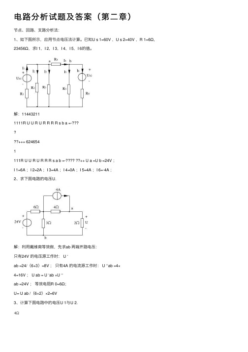
电路分析试题及答案(第⼆章)节点、回路、⽀路分析法:1、如下图所⽰,应⽤节点电压法计算。
已知U s 1=60V ,U s 2=40V ,R 1=6Ω, 23456Ω,求I 1,I 2,I 3,I 4,I 5,I 6的值。
解:114432111111R U U R U R R R R s b a =-+++ 6246541111R U U R U R R R s a b =-???? ??++ U a =U b =24V ;I 1=6A ;I 2=2A ;I 3=4A ;I 4=0A ;I 5=4A ;I 6=-4A ;2、求下图电路的电压U.解:利⽤戴维南等效做,先求ab 两端开路电压:只有24V 的电压源⼯作时: U ‘ab =24/(6+3)=8V ;只有4A 的电流源⼯作时: U ‘‘ab =4×4=16V ; U ab = U ‘ab +U ‘‘ab =24V ;等效电阻R 0=6Ω;U= U ab /(6+2)×2=6V3、计算下图电路中的电压U 1与U 2.解:U 1=8×[4+(6//3)]/[18+4+(6//3)] ×18=36V; U 2=8×18/[18×4+(6//3)] ×3=12V .4、已知下图电路的回路⽅程为2I 1+I 2=4V 和4I 2=8V ,式中各电流的单位为安培。
求:(1)各元件的参数;(2)各电压源供出的功率;(3)改变U和U 的值,使各电阻的功率增加⼀倍。
解:(1)1+ R 3)I 1+R 3I 2+k U 1=Us 1 1+ R 3-k R 1)I 1+R 3I 2 =Us 1-k Us 1R 3I 1 + (R 2+ R 3)I 2+k U 1=Us 2U 1=Us 1- R 1I 1 3-k R 1) I 1+ (R 2+ R 3)I 2+k U 1=Us 2-k Us 1R 1=2Ω, R 2=3Ω, R 3=1Ω, Us 1=8V , Us 1=12V , k =0.5 (2)求解⽅程式,得到:I 1=1A, I 2=2A ,计算各电源功率:Us 1:P 1= Us 1 I 1=8W ; (发出) Us 2:P 2= Us 2 I 2=24W ;(发出) Ucs :Pcs= Ucs (I 1+I 2)=9W ;(吸收)(3)各电源增加2倍,则各电阻上的电流相应增加2倍,即可实现⽬的。
- 1、下载文档前请自行甄别文档内容的完整性,平台不提供额外的编辑、内容补充、找答案等附加服务。
- 2、"仅部分预览"的文档,不可在线预览部分如存在完整性等问题,可反馈申请退款(可完整预览的文档不适用该条件!)。
- 3、如文档侵犯您的权益,请联系客服反馈,我们会尽快为您处理(人工客服工作时间:9:00-18:30)。
K
解)
(6A
=
闭合时: 总电阻Ω
=
+
⨯
+
=4
6
3
6
3
2
R
)
(5.7
4
30
30
1
A
R
I=
=
=
此时电流表的读数为:)
(5
5.7
3
2
6
3
6
1
A
I
I=
⨯
=
+
=
2-2 题2-2图示电路,当电阻R2=∞时,电压表12V;当R2=10Ω时,解:当∞
=
2
R时可知电压表读数即是电源电压
S
U.
.
12V
U
S
=
∴
当Ω
=10
2
R时,电压表读数:4
12
10
10
1
2
1
2=
⨯
+
=
+
=
R
U
R
R
R
u
S
(V)
Ω
=
∴20
1
R
2-3 题2-3图示电路。
求开关K打开和闭合情况下的输入电阻R i。
解:K )(18.60//(10Ω+=∴i R
K
)(8//30//(10Ω==∴i R
2-4 求题2-3图示电路的等效电阻R ab 、R cd 。
解:电路图可变为:
)
(1548
82.2148
82.2148//82.21)4040//10//(80//30)
(08.1782.294082
.294082.29//40)80//3040//10//(40)(4020
800)(8010800)
(4020
800
20201020202010123123Ω=+⨯==+=Ω=+⨯==+=Ω==Ω==Ω==⨯+⨯+⨯=cd
ab R R R R R 2-5 求题2-5图示电路的等效电阻 R ab 。
题2-59Ω
Ω
Ω
解:(a)图等效为:
5k Ω
4k Ω 4k Ω
8k Ω
a
b
5k Ω
2k Ω
8k Ω
a
b
)(73.315
56
8787)25//(8Ω==+⨯=+=∴ab R (b)图等效为:
5Ω
5Ω
15Ω a
b
3Ω
)(96325
150
3101510153)55//(153Ω=+=+=+⨯+=++=∴ab R
(c)图等效为:
b
a
9Ω
10Ω
5Ω
2Ω 4Ω
8Ω
注意到54210⨯=⨯,电桥平衡,故电路中9
电阻可断去
)(67.127
147
148)25//()410(8Ω=+⨯+=+++=∴ab R
(d)图等效为:
b
a
54Ω
14Ω R 12
R 23
R 31
)
(3618
648
1818981818912Ω==⨯+⨯+⨯=
R
)
(2272//)36//1436//54()
(722)(3612311223Ω=+=Ω==Ω==ab R R R R R
2-6 题2-6图示电路中各电阻的阻值相等,均为R ,求等效R ab .
(b)
(a)
解:e 、f 、g 电位点,所以 (a)图等效为:
)]//()(//[)(R R R R R R R R R R R ab +++++++=
R R R R R R R 4
5310//
2]
4//22//[2==+=
(b)图等效为:
])//()(//[)//()(R R R R R R R R R R R ab ++++++=
R
R
R R R R R R R R 75.0433//)
2//22//(2//22
===+=
2-7 化简题2-7图示各电路.
2
4
5V
102
8-
836-
解: (注:与电流源串联的元件略去,与电压源并联的元件略去)
(a)图等效为:
234-
(b)图等效为:
1
5
-
(d)图等效为:
7
6
-
(e)图等效为:
8
72
- (f)图等效为:
22
6V
-
2-8 用电源等效变换法求题2-8图示电路中负载R L 上的电压U .
+ -
14-
2
解:电路等效为:
+ -
7
U
+ -
5
5
-
U
+ -
1
5
-
U
+ -
5
+ -
1
3
+ -
U
+ -
2.5
)(3
10
5.725.22V U =⨯+=
2-9 题2-9图示电路.用电源等效变换法求电流i .
3
解:
3
1A
1A 55-
)(4
1
2051055105A i -=-=++-=
∴
2-10 若题2-10图示电路中电流i 为1.5A,问电阻R 的值是多少?
i
4Ω
6V
+ -
题2-10图
3Ω
R
2A
3A
解:流过R 的电流为i R =i -2=1.5-2= -0.5(A ),再利用电源等效变换,原电路等效为:
2A
4Ω
12A
13A
3Ω
R
i R
11A
i ’
4Ω//3Ω
i R
R
其中3
//4
=
Ω712,i ’=-1+0.5= -0.5(A ),)(7
12
Ω=∴R 2-11 化简题2-11图示电路.
i 0
(b)
4Ω
R 1
(a)
12
-
3Ω
2Ω
6Ω
0.5i 0
u S
-
+ u x -
R 2 gu x
b
a
b
a
题2-11图
解:(a)图等效为:
i 0
4Ω
3Ω 2Ω
6Ω
0.5i 0
b
a
4
b
a
4
8
-
2
a
8-
4
b
a
2
b
a
2
2
4-i
a
b
2 a
b
-1
1 a
b
(b)图:设端口电流为i ,则01=++i gu R u x x i gR R u x 1
1
1+-=∴ 原电路变为:
a
a
1
1
12111)1(gR R gR gR R +=
+-+
2-12 求题2-12图示电路中电流源和电压源提供的功率分别是多少?
2
Ω
解:电流源发出功率为)(20102w P =⨯=
原图可变为:
Ω
Ω
2A
2.21Ω
2A
)
(21.221.11)9
14
1142//(9141)2//76//221//(7//21)
(7),(2
21
),(73323233231312Ω=+=++=++=∴Ω=Ω=Ω=⨯+⨯+⨯=
总R R R R
)(32.452
w R U P ==∴总
总
∴电压源发出的功率P =45.32-20=25.32(w ) 2-13 求题2-13图示电路a 、b 端的等效电阻R ab .
Ω
解:原电路等效为:
1Ω
Ω
0.5Ω
Ω
)(35.220
47
)67//
21(2
Ω==+=∴ab R。