
AS1117-BQFT;中文规格书,Datasheet资料
The AS1117 is ideal for seven-segment or dot matrix user interface displays of mobile applications, set-top boxes, VCRs, DVD-players, washing machines, micro wave ovens, refrigerators and other white good or personal electronic applications.
Keyscan Input. Keyscan lines for key readback. Can be used for self-adressing. Reset Input. Pull this pin to low to resest all registers (set to default values) and to put the device into shutdown. Connect this pin via a pull-up resistor to VDD for normal operation. Set Segment Current. Connect to VDD or a reference voltage through RSET to set the peak segment current (see Selecting RSET Resistor Value and Using External Drivers on page 19). Serial-Clock Input. 3.4MHz maximum rate.
Stresses beyond those listed in Table 3 may cause permanent damage to the device. These are stress ratings only, and functional operation of the device at these or any other conditions beyond those indicated in Section 6 Electrical Characteristics on page 4 is not implied. Exposure to absolute maximum rating conditions for extended periods may affect device reliability.
Figure 1. AS1117 - Typical Application Diagram
VDD 2.7V to 5.5V
9.53kΩ
VDD
DIG0 to
DIG7
8
ISET
SEGA-DP
KEY0-7
8
SDA SCL µ1117
KEY
GND
/LED-Driver-ICs/AS1117 /
30.5
-40
+85
-55
150
kV
mA ºC/W
ºC ºC
Norm: MIL 833 E method 3015
EIA/JESD78 on PCB
Package Body Temperature
+260
The reflow peak soldering temperature (body temperature) specified is in accordance with IPC/ JEDEC J-STD-020D “Moisture/ ºC Reflow Sensitivity Classification for Non-Hermetic Solid State Surface
Table 2. Pin Descriptions
Pin Name SDA
DIG0:DIG7
GND KEY
RESETN
ISET
SCL IRQ SEGA:SEGG, SEGDP VDD
Pin Number 22
1, 2, 4, 5, 6, 7, 23, 24 3 8
9
10
11 21 12-15, 17-20
16
Exposed Pad
Description Serial-Data I/O. Open drain digital I/O I²C data pin. Digit Drive Lines. Eight digit drive lines that sink current from the display common cathode. Keyscan detection optional, but must be polled by the µProzessor. Ground.
Revision 1.00
1 - 23
AS1117
Datasheet - Pinout
4 Pinout
Pin Assignments
Figure 2. Pin Assignments (Top View)
DIG1 DIG0 SDA IRQ SEGD SEGDP
24 23 22 21 20 19
DIG2 1
500
mA
100
mA
Humidity
5
85
%
Non-condensing
ESD
Digital outputs All other pins
Latch-Up Immunity
Thermal Resistance ΘJA
Ambient Temperature
Storage Temperature
1
±100
Table 3. Absolute Maximum Ratings
Parameter
Min
Max Units
Notes
Input Voltage Range
VDD to GND All other pins to GND
-0.3
7
V
-0.3
7 or VDD + 0.3
V
Current
DIG0:DIG7 Sink Current SEGA:SEGG, SEGDP
Interupt Request Output. Open drain pin. Seven Segment and Decimal Point Drive Lines. 8 seven-segment drives and decimal point drive that source current to the display. Positive Supply Voltage. Connect to +2.7V to +5.5V supply. Bypass this pin to GND with a 0.1µF capacitor to avoid power supply ripple. Exposed Pad. This pin also functions as a heat sink. Solder it to a large pad or to the circuit-board ground plane to maximize power dissipation.
/LED-Driver-ICs/AS1117 /
Revision 1.00
2 - 23
AS1117
Datasheet - Absolute Maximum Ratings
5 Absolute Maximum Ratings
- Global or Individual Error Detection ! Hexadecimal- or BCD-Code for 7-Segment Displays ! 200nA Low-Power Shutdown Current (typ; data
retained) ! Digital and Analog Brightness Control ! Display Blanked on Power-Up ! Drive Common-Cathode LED Displays ! Supply Voltage Range: 2.7V to 5.5V ! Software and Hardware Reset ! Up to 4 devices cascadable ! Optional External Clock ! Package: TQFN(4x4)-24
18 SEG E
DIG3 2
17 SEGC
GND 3 DIG4 4
AS1117
16 VDD 15 SEGG
DIG5 5 DIG6 6
Exposed Pad
14 SEGB 13 SEGF
7 8 9 10 11 12
DIG7 KEY RESETN ISET SCL SEGA
Pin Descriptions
The devices include an integrated BCD code-B/HEX decoder, multiplex scan circuitry, segment and display drivers, and a 64-bit memory. Internal memory stores the shift register settings, eliminating the need for continuous device reprogramming.
Datasheet
AS1117
64 LED Driver for Mobile Applications with Error Detection
1 General Description
The AS1117 is a compact LED driver for 64 single LEDs or 8 digits of 7-segments. The devices can be programmed via an I²C compatible 2-wire interface. Every segment can be individually addressed and updated separately. Only one external resistor (RSET) is required to set the current. LED brightness can be controlled by analog or digital means.
1117中文资料
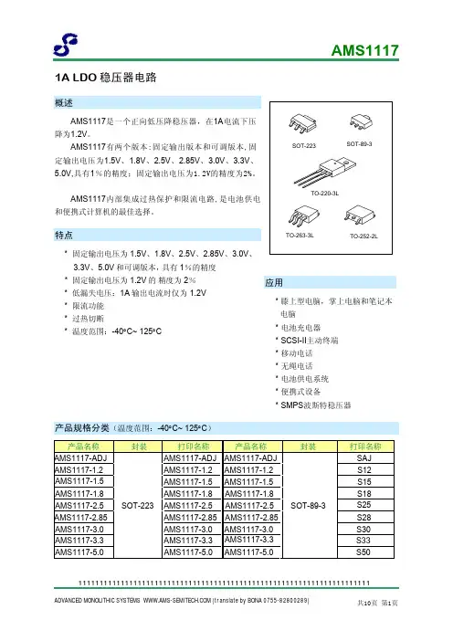
管脚名称 GND/ADJ
VOUT VIN
I/O
--/O 地/ADJ。
O
输出电压。
I
输入工作电压。
功能
1111111111111111111111111111111111111111111111111111111111111111111111111111111111
ADVANCED MONOLITHIC SYSTEMS (translate by BONA 0755-82800289)
封装 TO-252-2L TO-263-3L
打印名称
AMS1117-ADJ AMS1117-1.2 AMS1117-1.5 AMS1117-1.8 AMS1117-2.5 AMS1117-2.85 AMS1117-3.0 AMS1117-3.3 AMS1117-5.0 AMS1117-2.85 AMS1117-3.0 AMS1117-3.3 AMS1117-5.0
AMS1117-1.5, IOUT=10mΑ, VIN=3.5V ,TJ=25°C 10mA≤IOUT≤1A, 3.0V≤VIN≤10V
1.176 1.2 1.224 V 1.152 1.2 1.248
1.485 1.500 1.515 V 1.470 1.500 1.530
VOUT AMS1117-1.8,
V
0≤IOUT≤1A, 4.25V≤VIN ≤10V
2.790 2.850 2.910
0≤IOUT≤500mA, VIN =4.10V
2.790 2.850 2.910
AMS1117-3.0,
IOUT=10mA, VIN=4.5V,TJ=25°C , 2.970 3.000 3.030 V
VOUT 0≤IOUT≤1A, 4.4V≤VIN≤10V
AS5013-IQFT-1000;中文规格书,Datasheet资料

2 Key Features
2.7V to 3.6V operating voltage Down to 1.7V peripheral supply voltage Two operating modes:
- Idle mode - Low power mode
Less than 3µA current consumption in Idle mode Low power mode with selectable readout rate Two interrupt modes
Datashee t
AS5013
Low Power Integrated Hall IC for Human Interface Applications
1 General Description
The AS5013 is a complete Hall Sensor IC for smart navigation key applications to meet the low power requirements and host SW integration challenges for products such as cell phones and smart handheld devices. Due to the on chip processing engine, system designers are not tasked with integrating complex SW algorithms on their host processor thus leading to rapid development cycles. The AS5013 single-chip IC includes 5 integrated Hall sensing elements for detecting up to ±2mm lateral displacement, high resolution ADC, XY coordinate and motion detection engine combined with a smart power management controller. The X and Y positions coordinates and magnetic field information for each Hall sensor element is transmitted over a 2-wire I²C compliant interface to the host processor. The AS5013 is available in a small 16-pin 4x4x0.55mm QFN package and specified over an operating temperature of -20ºC to +80ºC.
AMS1117 DATASHEET原厂规格书

1A Adjustable/Fixed Low Dropout Linear Regulator- Low dropout voltage- Load regulation: 0.2% typical - Optimized for Low V oltage - On-chip thermal limiting- Standard SOT-223 and TO-252 packages- Three-terminal adjustable or fixed low dropout 1.2V ,1.5V ,1.8V , 2.5V , 2.85V , 3.3V , 5V . Regulators- Active SCSI terminators- High efficiency linear regulators- Post regulators for switching supplies - Battery chargers- 12V to 5V linear regulators - M otherboard clock suppliesThe AMS 1117-ADJ and AMS 1117-1.2,-1.5,-1.8,-2.5,-2.85, -3.3 and-5 are low dropout three-terminal regulators with 1A output current capability. These devices have been optimized for low voltage where transient response and minimum input voltage are critical. The 2.85V version is designed specifically to be used in Active Terminators for SCSI bus.On-chip thermal limiting provides protection against any combination of overload and ambient temperatures that would create excessive junction temperatures.Unlike PNP type regulators where up to 10% of the output current is wasted as quiescent current, the quiescent cur-rent of the AMS 1117 flows into the load, increasing effi-ciency.The AMS 1117 series regulators are available in the indus-try-standard SOT-223 and TO-252 power packages.Key FeaturesApplicationsGeneral DescriptionTypical ApplicationNotice: The distance between V out pin and Capacitor should not exceed 4cm for excellent performanceFigure 1. Typical Applications of AMS 11171A Adjustable/Fixed Low Dropout Linear RegulatorPin Assignments*With package soldered to 0.5 square inch copper area over backside ground plane or internal power plane, ΘJA can vary from 30°C/W to more than 50°C/W. Other mounting techniques may provide better thermal resistance than 30°C/W.Absolute Maximum RatingsFigure 2. Pin Assignments of AMS 1117ParameterMin.Max.UnitV IN 18 V(V IN – V OUT ) * I OUTSee Figure 3Operating Junction Temperature Range -20 125°C Storage Temperature Range-65150°C Lead Temperature (Soldering, 10 sec.) 300°C1A Adjustable/Fixed Low Dropout Linear RegulatorTypicals and limits appearing in normal type apply for T J =25℃.Limits appearing in Boldface type apply over the entire junction temperature for operation, -20℃to 125℃.Electrical CharacteristicBlock DiagramThermal LimitCurrent LimitV OUTV INSubstrateGND (fixed output) ADJ. (adjustable output)Figure 3. Block Diagram of AMS 1117SymbolParameterConditionsMin (Note 2) Typ (Note 1) Max(Note 2)UnitsV REFReference VoltageAMS 11171.5V<=(V IN -V OUT )<=7V,10mA<=I OUT <=1A1.225 1.250 1.275 VV OUT OutputVoltage 10mA<=I OUT <=1AI OUT = 10mA, V IN = 3.2V AMS 1117-1.2 ,2.7V<= V IN <=8.2V 1.176 1.152 1.200 1.200 1.224 1.248 V AMS 1117-1.5 ,3.0V<= V IN <=8.5V1.4701.5001.530VAMS 1117-1.8 ,3.3V<= V IN <=8.8V 1.764 1.800 1.836 VAMS 1117-2.5 ,4V<= V IN <= 9.5V 2.450 2.500 2.550 V AMS 1117-2.85 , 4.35V <= V IN <= 9.85V 2.793 2.850 2.907 V AMS 1117-3.3 , 4.8V<= V IN <=10.3V 3.234 3.300 3.366 V AMS 1117-5.0,6.5V<=V IN <= 12V4.9005.0005.100V1A Adjustable/Fixed Low Dropout Linear RegulatorTypicals and limits appearing in normal type apply for T J =25℃.Limits appearing in Boldface type apply over the entire junction temperature for operation, -20℃ to 125℃.Electrical Characteristic(Continued)SymbolParameter ConditionsMin (Note 2)Typ (Note 1) Max (Note 2) Units △V OUTLine Regultion (Note 3)I OUT =10mA ,(V OUT +1.5V)<=V IN <=12V 0.035 0.2 % Load Regultion (Note 3) V IN -V OUT =2V,10mA<= I OUT <=1A,0.2 0.7 % AMS 1117-1.2V IN -V OUT =2V,10mA<= I OUT <=1A,0.2 1 % V IN -V OUTDropout Volage I OUT =1A,△V REF =1% 1.100 1.250 V I LimitCurrent Limit V IN -V OUT = 2V, T J =25℃1.1 1.5A Minimum Load Current (Note 4) AMS 1117-ADJ1.5V<=(V IN -V OUT )<=10V10mA Quiescent CurentV IN =V OUT +1.25V 5 13 mA Thermal Regulation T A = 25°C, 30ms pulse 0.01 0.1 %/W RippleRejection f=120Hz,V IN -V OUT =3V, V Ripple =1V PP60 72 dB Adjust Pin Current50120µAAdjust Pin CurrentChange 1.5V<=V IN -V OUT <=7V, 10mA<=I OUT <=1A0.2 5 µATemperature Stability0.5 % Long Term StabilityT A = 125°C, 1000hrs.0.3%1A Adjustable/Fixed Low Dropout Linear RegulatorNote 1: Typical Values represent the most likely parametric norm. Note 2: All limits are guaranteed by testing or statistical analysis.Note 3: Load and line regulation are measured at constant junction room temperature. Note 4: The minimum output current required to maintain regulation.Typical Performance CharacteristicsTypicals and limits appearing in normal type apply for T J =25℃.Limits appearing in Boldface type apply over the entire junction temperature for operation, -20℃to 125℃.Electrical Characteristic(Continued)Symbol ParameterConditionsMin (Note 2) Typ (Note 1) Max (Note 2)UnitsI LimitRMS Output Noise(% ofV OUT )T A = 25°C, 10Hz<= f <=10kHz0.003 % Thermal Resistance, Junctionto CaseSOT-223 15 ℃/W TO-252 3 ℃/W Thermal Shutdown Junction Temperature155 ℃ Thermal Shutdown Hysteresis25℃Output Current ( A )0 0.2 0.4 0.6 0.8 1.01.5 1.4 1.3 1.2 1.0 0.9 0.8 0.7 0.6 0.5 0D r o p o u t V o l t a g e ( V )Figure 4. Dropout Voltage VS. Output Current1A Adjustable/Fixed Low Dropout Linear RegulatorTypical Performance Characteristics(Continued)Figure 6. Output Voltage VS. TemperatureO u t p u t V o l t a g e ( V )3.70 3.65 3.603.553.50 3.45 3.40 3.35 3.30 3.253.20Junction Temperature ( ℃ )-75 –50 –25 0 25 50 75 100 125 150 175Figure 5. Reference Voltage VS. TemperatureR e f e r e n c e V o l t a g e ( V )0.260 1.255 1.250 1.245 1.240 1.235 1.225 1.220 1.215 1.210Junction Temperature ( ℃ )-75 –50 –25 0 25 50 75 100 125 150 175Figure 7. Minimum Load Current VS. TemperatureM i n i m u m L o a d C u r r e n t ( m A )5 4 3 2 1Junction Temperature ( ℃ ) -75 –50 –25 0 25 50 75 100 125 150 175Figure 8. ADJ Pin Current VS. TemperatureA D J P i n C u r r e n t ( µA ) 100 90 807060 50 40 30 20 10 0Junction Temperature ( ℃ ) -75 –50 –25 0 25 50 75 100 125 150 175Note:AMS 1117 OnlyAMS11171AAdjustable/Fixed Low Dropout Linear RegulatorMechanical Dimensions4-Lead SOT-223 PackageSymbolInches Millimeters NotesMin.Max.Min. Max.A Ñ .071 Ñ 1.80 A1 Ñ .181 Ñ 4.80B .025 .033 .064 .840 c Ñ 0.90 Ñ 2.29 D .248 .264 6.30 6.71 E .130 .148 3.30 3.71 e .115 .124 2.95 3.15 F .033 .041 .840 1.04 H .264 .287 6.71 7.29 I .0121 Ñ .310 Ñ J Ñ 10° Ñ 10° K 10° 16° 10° 16° L.0008 .0040 .0203 .1018 M 10° 16° 10° 16° N.010.014.250.360Figure 9. 4-Lead SOT-223 Package1A Adjustable/Fixed Low Dropout Linear RegulatorMechanical Dimensions(Continued)3-Lead TO-252 PackageNotes:1. Dimensions are exclusive of mold flash, metal burrsor interlead protrusion.2. Stand off-height is measured from lead tip with ref. toDatum –B-.3. Foot length is measured with ref. to Datum –A– withlead surface. 4. Thermal pad contour optional within dimension b3 and L3.5. Formed leads to be planar with respect to one anotherat seating place –C-.6. Dimensions and tolerances.SymbolInchesMillimetersNotesMin. Max.Min. Max.A .086 .094 2.19 2.39 b .025 .035 0.64 0.89 b2 .030 .045 0.76 1.14 b3 .205 .215 5.12 5.46 4 c .018 .024 0.46 0.61 c2 .018 .023 0.46 0.58 D .210 .245 5.33 6.22 1E .250 .265 6.35 6.73 1e .090 BSC 2.29 BSCH .370 .410 9.40 10.41 L .055 .070 1.40 1.78 3 L1 .108 REF 2.74 REFL3 .035 .080 0.89 2.03 4 L4.025.0400.641.02Figure 10. 3-Lead TO-252 Package1A Adjustable/Fixed Low Dropout Linear R egulatorAdvanced Monolithic Systems The " " logo is a registered trademark of Advanced Monolithic Systems.All other company and product names are trademarks of their respective ownersOrdering InformationPackage Temperature Range Part Number Output Voltage Packing Marking Transport MediaSOT -223-20℃ - +125℃ AMS 1117-1.2 1.2V AMS 1117 1.2 2.5K Tape and Reel -20℃ - +125℃ AMS 1117-1.5 1.5V AMS 1117 1.5 2.5K Tape and Reel -20℃ - +125℃ AMS 1117-1.8 1.8V AMS 1117 1.8 2.5K Tape and Reel-20℃ - +125℃ AMS 1117-2.5 2.5V AMS 1117 2.5 2.5K Tape and Reel -20℃ - +125℃ AMS 1117-2.85 2.85V AMS 1117 2.8 2.5K Tape and Reel -20℃ - +125℃ AMS 1117-3.3 3.3V AMS 1117 3.3 2.5K Tape and Reel -20℃ - +125℃ AMS 1117-5 5V AMS 1117 5 2.5K Tape and Reel -20℃ - +125℃ AMS 1117 Adjust AMS 1117 2.5K Tape and Reel TO -252-20℃ - +125℃ AMS 1117-1.2 1.2V AMS 1117 1.2 2.5K Tape and Reel -20℃ - +125℃ AMS 1117-1.5 1.5V AMS 1117 1.5 2.5K Tape and Reel -20℃ - +125℃ AMS 1117-1.8 1.8V AMS 1117 1.8 2.5K Tape and Reel-20℃ - +125℃ AMS 1117-2.5 2.5V AMS 1117 2.5 2.5K Tape and Reel -20℃ - +125℃ AMS 1117-2.85 2.85V AMS 1117 2.8 2.5K Tape and Reel -20℃ - +125℃ AMS 1117-3.3 3.3V AMS 1117 3.3 2.5K Tape and Reel -20℃ - +125℃ AMS 1117-5 5.0V AMS 1117 5 2.5K Tape and Reel -20℃ - +125℃ AMS 1117CD Adjust AMS 1117CD 2.5K Tape and ReelDisclaimer:• AMS reserves the right to make changes to the information herein for the improvement of the design and performancewithout further notice! Customers should obtain the latest relevant information before placing orders and should verify that such information is complete and current.• All semiconductor products malfunction or fail with some probability under special conditions. When using AMS productsin system design or complete machine manufacturing, it is the responsibility of the buyer to comply with the safety standards strictly and take essential measures to avoid situations in which a malfunction or failure of such AMS products could cause loss of body injury or damage to property.• AMS will supply the best possible product for customers!。
AS1117中文资料

8-Pin Surface Mount (S)
TO-220-3 (U)
SOT-89 (M1)
SOT-223 (M3)
TO-263-3 (T)
TO-252 (R)
GND N/C VOUT VOUT
1
82Biblioteka 7ALPHA3 AS1117 6
4
5
Top View
V IN
ALPHA
VIN
ALPHA
AS1117 123
The AS1117 is offered in a 3-pin surface mount package SOT-223, TO-252, TO-220, SOT-89 & TO-263. The output capacitor of 10µF or larger is needed for output stability of AS1117 as required by most of the other regulator circuits. Use of ALPHA Semiconductor’s design, processing and testing techniques make our AS1117 superior over similar products.
V IN
AS1117 123
N/C
ADJ/GND VOUT VIN
Top View
ADJ/GND
VOUT
V
IN
Front View
ALPHA AS1117 1 23
ADJ/GND VOUT VIN Top View
ALPHA AS1117 123
ADJ/GND VOUT VIN Top View
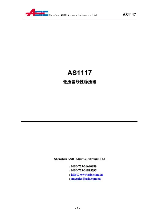
AS1117低压差线性稳压器说明书
热稳定性
4
8
mA
55
120
uA
0.2
uA
0.5
%
θJC
热阻
20
℃/W
注释:
Note1:表中所给出的电压线性度和负载线性度的参数是在常温下测试的。负载线性度随 温度的 变化曲线请参看后面的典型参数曲线。
Note2:常温下,当 Iout 在 0~1A 之间,Vin-Vout 在 1.5V 和 12 之间变化时,满足表中给 出的规范范围。若温度在如下范围-50℃≤TA≤140℃内变化时,也要求满足表中 所给出的规范,则输出电流 Iout 需大于 10mA。
最大负载电流 Vin-Vout=2V, Tj=25℃
Ilimit
最小负载电流 (note4) AS1117-ADJ
Iq
静态电流
AS1117-1.8V,Vin-Vout=1.25V
1.25
1.4
1.6
A
5
10
mA
4
8
mA
-5-
深圳市爱思科微电子有限公司 Shenzhen ASIC Micro-electronics Ltd.
AS1117 可调版本应用图 2 -7-
深圳市爱思科微电子有限公司 Shenzhen ASIC Micro-electronics Ltd.
AS1117
说明:
可调版本的输出电压等于 Vout=Vref*(1+R2/R1)+IAdj*R2,由于 IAdj 较小(50uA 左右), 远小于流过 R1 的电流(4mA 左右),因此可忽略。
2.525
V
2.45
2.5
2.55
Vout 输出电压
AS1117-2.85V Iout=10mA,Vin=4.85V,Tj=25℃ 0≤Iout≤1A ,4.25V≤Vin≤12V
SPX1117中文数据手册
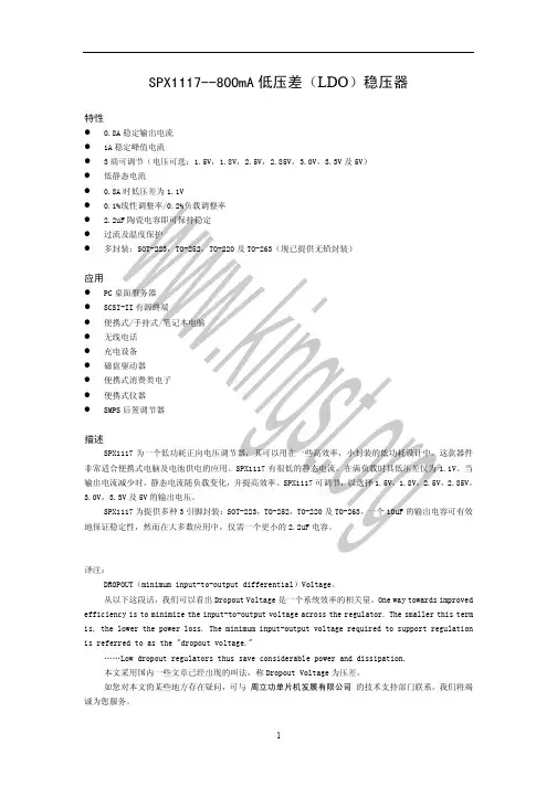
表1 PC 板(mm2) 2500 2500
图 20 纹波抑制比;Vin=3.3V,Vout=1.8V(adj.),Iload=200mA
顶层 Copper(mm2) 2500 1250
背层 Copper(mm2) 2500 2500
热阻(JUNC to AMB) ℃/W 46 47
2500
950
2500
(VIN-VOUT)=5V 25℃,30mS 脉冲 fRIPPLE=120Hz,VIN-VOUT=2V, VRIPPLE=1VPP 125℃,1000Hrs Vout 百分比,10Hz≤f≤10kHz TO-220 接点->焊片 TO-220 接点->周围环境 TO-263 接点->焊片 TO-263 接点->周围环境 TO-252 接点->焊片
4
图5 SPX11173M3-3.3电流极限值,Iout从10mA到1A时的输出电压偏差 图 6 Vout vs 温度,VIN=2.5V,IOUT=10mA 图 7 VIN=3.0V,IOUT=10mA 图 8 VIN=3.3V,IOUT=10mA 5
图9 VIN=4.0V,IOUT=10mA 图 10 VIN=4.85,IOUT=10mA 图 11 VIN=4.85,IOUT=10mA 图 12 VIN=5.0V,IOUT=10mA 图 13 线性调节率 Vs 温度,Vout=1.8V(可调节),VIN=3.3V 6
+ 1.5V
3
图1 SPX1117M3-3.3负载调节率;VIN=4.8V 图 2 SPX1117M3-3.3 线性调节率;IOUT=10mA 图 3 SPX1117M3-3.3 压差 vs 输出电流;VIN=4.8V,COUT=2.2uF 图 4 SP1117M3-3.3 的电流极限值;VIN=4.8V,CIN=COUT=1uF,IOUT 从 10mA 到电流极限值
AAT1117中文资料
元器件交易网
$1$/2*,&
7(&+
Symbol VOUT ∆VOUT/ VOUT ∆VOUT/ VOUT VDO ILIM IQ TC ∆V/∆T VN PSRR Description Output Voltage
TM
AAT1117
1117.2000.05.0.92
元器件交易网
$1$/2*,&
7(&+
Symbol
VIN IOUT TJ ΘJA ΘJA ΘJA PD PD PD TLEAD
TM
AAT1117
1 Amp Linear Regulator
Absolute Maximum Ratings (TA=25°C unless otherwise noted)
1 Amp Linear Regulator
Electrical Characteristics AAT1117-3.3 (fixed)(TJ=25°C unless otherwise noted)
Conditions VIN = 5V, IOUT = 0A TJ=25°C Full temp Min 3.270 3.234 Typ 3.30 3.30 Max 3.330 3.336 0.2 0.3 0.4 0.3 0.4 1.2 % Units V
The AAT1117 is a Positive Linear Regulator designed to deliver 1 amp. It features adjustable or fixed output voltages and excellent performance over line and load variations. The device is able to protect itself and the load from short circuit conditions with integrated current limiting circuitry. Thermal shutdown is activated to prevent damage under extreme conditions. The AAT1117 is available in surface mount SOT223 or TO-252 (DPAK), and through-hole TO-220 packages.
LD1117系列各品牌技术规格书
ABSOLUTE MAXIMUM RATINGS (Note 1)
Power Dissipation
Internally limited
Input Voltage
15V
Operating Junction Temperature Range
Control Section
0°C to 125°C
Power Transistor
Adjust Pin Current Change
Temperature Stability
Long Term Stability
RMS Output Noise (% of VOUT ) Thermal Resistance Junction-to-Case
2.82
2.850
2.88
V
2.79
2.850
2.91
V
0 ≤ IOUT ≤ 800mA , 4.75V ≤ VIN ≤ 12V
3.267 3.300
3.333
V
3.235 3.300
3.365
V
0 ≤ IOUT ≤ 800mA , 6.5V ≤ VIN ≤ 12V
4.950 5.000
5.050
V
ϕ JA= 90°C/W*
* With package soldering to copper area over backside
2SJ117中文资料(hitachi)中文数据手册「EasyDatasheet - 矽搜」
脉冲测试
–2 漏电流I
–1
TC = –25°C
25°C 75°C
0
–2 –4
门源电压V
–6 –8 –10 GS (V)
3
芯片中文手册,看全文,戳
2SJ117
(V) –20
DS (on)
–16
漏极至源极饱和电压 与门源电压
–12
–8
–4
脉冲测试
漏极至源极饱和电压V
–5 –10 –20 D (A)
静态漏极至源关于国家
电阻与温度
10 VGS = 15 V ID = –1 A
8
(Ω) 6
DS (on)
R4
2
静态漏极至源极导通电阻
0 –40 0 40
案例温T
80 120 160 C (°C)
1,0000 3,000
典型的电容与 漏源极电压
VGS = 0 F = 1兆赫
漏极至源极电压V
DS (V)
典型的输出特性
–2.0 –15 V 0V
–1
–1.6
(A)
TC = 25°C
–6 V –5 V
D
–1.2
–4.5 V
–0.8 漏电流I
–4 V –0.4
VGS = –3 V
0
–4 –8 –12 –16 –20
漏极至源极电压V
DS (V)
–5
–4 (A)
D
–3
典型的传输特性
1,000 300
电容C(1P0F0) 30
Ciss Coss
10
Crss
3
1 0 –40 –80 –120 –160 –200
漏极至源极电压V
744227;中文规格书,Datasheet资料
8.1 8.0 7.02012-07-172012-07-172004-10-11SStSStMSTSStSBaWürth Elektronik eiSos GmbH & Co. KGEMC & Inductive SolutionsMax-Eyth-Str. 174638 WaldenburgGermanyTel. +49 (0) 79 42 945 - 0A Dimensions: [mm]F Typical Impedance Characteristics:H1: Classification Reflow Profile for SMT components:H2: Classification Reflow ProfilesProfile FeaturePreheat- Temperature Min (T smin ) - Temperature Max (T smax ) - Time (t s ) from (T smin to T smax )Ramp-up rate (T L to T P )Liquidous temperature (T L )Time (t L ) maintained above T L Peak package body temperature (T p )Time within 5°C of actual peak temperature (t p )Ramp-down rate (T P to T L )Time 25°C to peak temperature Pb-Free Assembly 150°C 200°C60-180 seconds 3°C/ second max.217°C60-150 seconds See Table H320-30 seconds 6°C/ second max.8 minutes max.refer to IPC/JEDEC J-STD-020DH3: Package Classification Reflow TemperaturePB-Free Assembly PB-Free Assembly PB-Free Assembly Package Thickness< 1.6 mm 1.6 - 2.5 mm ≥ 2.5 mmVolume mm³<350260°C 260°C 250°CVolume mm³350 - 2000260°C 250°C 245°CVolume mm³>2000260°C 245°C 245°Crefer to IPC/JEDEC J-STD-020DH Soldering Specifications:I Cautions and Warnings:The following conditions apply to all goods within the product series of WE-SL2of Würth Elektronik eiSos GmbH & Co. KG:General:All recommendations according to the general technical specifications of the data sheet have to be complied with.The disposal and operation of the product within ambient conditions which probably alloy or harm the wire isolation has to be avoided.If the product is potted in customer applications, the potting material might shrink during and after hardening. Accordingly to this the product is exposed to the pressure of the potting material with the effect that the core, wire and termination is possibly damaged by this pressure and so the electrical as well as the mechanical characteristics are endanger to be affected. After the potting material is cured, the core, wire and termination of the product have to be checked if any reduced electrical or mechanical functions or destructions have occurred.The responsibility for the applicability of customer specific products and use in a particular customer design is always within the authority of the customer. All technical specifications for standard products do also apply for customer specific products.Cleaning solvents which are used to clean the application might damage or change the characteristics of the component.Direct mechanical impact to the product shall be prevented as the ferrite material of the core could flake or in the worst case it could break. Product specific:Follow all instructions mentioned in the datasheet, especially:•The soldering profile has to be complied with according to the technical reflow soldering specification, otherwise no warranty will be su-stained.•All products are supposed to be used before the end of the period of 12 months based on the transfer of title, if not a 100% solderability can´t be warranted.•Violation of the technical product specifications such as exceeding the nominal rated current will result in the loss of warranty.1. General Customer ResponsibilitySome goods within the product range of Würth Elektronik eiSos GmbH & Co. KG contain statements regarding general suitability for certain application areas. These statements about suitability are based on our knowledge and experience of typical requirements concerning the are-as, serve as general guidance and cannot be estimated as binding statements about the suitability for a customer application. The responsibi-lity for the applicability and use in a particular customer design is always solely within the authority of the customer. Due to this fact it is up to the customer to evaluate, where appropriate to investigate and decide whether the device with the specific product characteristics described in the product specification is valid and suitable for the respective customer application or not.2. Customer Responsibility related to Specific, in particular Safety-Relevant ApplicationsIt has to be clearly pointed out that the possibility of a malfunction of electronic components or failure before the end of the usual lifetime can-not be completely eliminated in the current state of the art, even if the products are operated within the range of the specifications.In certain customer applications requiring a very high level of safety and especially in customer applications in which the malfunction or failure of an electronic component could endanger human life or health it must be ensured by most advanced technological aid of suitable design of the customer application that no injury or damage is caused to third parties in the event of malfunction or failure of an electronic component.3. Best Care and AttentionAny product-specific notes, warnings and cautions must be strictly observed.4. Customer Support for Product SpecificationsSome products within the product range may contain substances which are subject to restrictions in certain jurisdictions in order to serve spe-cific technical requirements. Necessary information is available on request. In this case the field sales engineer or the internal sales person in charge should be contacted who will be happy to support in this matter.5. Product R&DDue to constant product improvement product specifications may change from time to time. As a standard reporting procedure of the Product Change Notification (PCN) according to the JEDEC-Standard inform about minor and major changes. In case of further queries regarding the PCN, the field sales engineer or the internal sales person in charge should be contacted. The basic responsibility of the customer as per Secti-on 1 and 2 remains unaffected.6. Product Life CycleDue to technical progress and economical evaluation we also reserve the right to discontinue production and delivery of products. As a stan-dard reporting procedure of the Product Termination Notification (PTN) according to the JEDEC-Standard we will inform at an early stage about inevitable product discontinuance. According to this we cannot guarantee that all products within our product range will always be available. Therefore it needs to be verified with the field sales engineer or the internal sales person in charge about the current product availability ex-pectancy before or when the product for application design-in disposal is considered.The approach named above does not apply in the case of individual agreements deviating from the foregoing for customer-specific products.7. Property RightsAll the rights for contractual products produced by Würth Elektronik eiSos GmbH & Co. KG on the basis of ideas, development contracts as well as models or templates that are subject to copyright, patent or commercial protection supplied to the customer will remain with Würth Elektronik eiSos GmbH & Co. KG.8. General Terms and ConditionsUnless otherwise agreed in individual contracts, all orders are subject to the current version of the “General Terms and Conditions of Würth Elektronik eiSos Group”, last version available at .J Important Notes:The following conditions apply to all goods within the product range of Würth Elektronik eiSos GmbH & Co. KG:分销商库存信息: WURTH-ELECTRONICS 744227。