MDCSIM A COMPILED EVENT-DRIVEN MULTI- DELAY SIMULATOR
fdk-aac编码原理

fdk-aac编码原理
fdk-aac是一种开源的、高性能的AAC(Advanced Audio Coding)音频编码库。
以下是fdk-aac编码的基本原理:
1.AAC编码概述:AAC是一种先进的音频编码标准,旨在提供更高的音频质量和更低的比特率。
它采用了基于子带的编码技术,通过对音频信号进行频域分析和量化来实现高效的压缩。
2.Psychoacoustic Model(心理声学模型):AAC编码使用心理声学模型分析音频信号,模拟人耳的感知特性。
这包括对音频信号的掩蔽效应进行建模,以便更有效地分配比特率给对人耳更敏感的信号部分。
3.MDCT(Modulated Discrete Cosine Transform):AAC使用MDCT作为频域变换技术,将音频信号从时域变换到频域。
这种变换有助于提取信号的频域特征,为后续的量化和编码提供基础。
4.Quantization and Coding(量化和编码):MDCT输出的频域系数经过量化和编码,以减少数据量。
AAC使用了一系列的编码技术,如Huffman编码和熵编码,来进一步压缩数据。
5.Bit Allocation(比特分配):根据心理声学模型的分析结果,AAC对每个频带分配适当的比特率,以确保对人耳敏感的频段获得更多的比特,从而提高音质。
6.码率控制:AAC编码器通常具有码率控制功能,以确保生成的编码流满足指定的比特率要求。
这对于网络传输和存储空间的有效利用非常重要。
fdk-aac是一个高度优化的AAC编码库,它在实现这些基本原理的同时,通过一系列的技术手段和算法来提高编码效率和音频质量。
Tektronix MDO3000 Series 数字多功能作业仪用户指南说明书
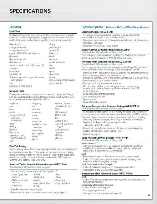
19StandardMath ToolsDisplay up to four math function traces (F1-F4). The easy-to-use graphical interface simplifies setup of up to two operations on each function trace;and function traces can be chained together to perform math-on-math.absolute value integralaverage (summed)invert (negate)average (continuous)log (base e)custom (MATLAB) – limited points product (x)derivativeratio (/)deskew (resample)reciprocaldifference (–)rescale (with units)enhanced resolution (to 11 bits vertical)roof envelope (sinx)/x exp (base e)square exp (base 10)square root fft (power spectrum, magnitude, phase,sum (+)up to 50 kpts) trend (datalog) of 1000 events floorzoom (identity)histogram of 1000 eventsMeasure ToolsDisplay any 6 parameters together with statistics, including their average,high, low, and standard deviations. Histicons provide a fast, dynamic view of parameters and wave-shape characteristics.Pass/Fail TestingSimultaneously test multiple parameters against selectable parameter limits or pre-defined masks. Pass or fail conditions can initiate actions including document to local or networked files, e-mail the image of the failure, save waveforms, send a pulse out at the rear panel auxiliary BNC output, or (with the GPIB option) send a GPIB SRQ.Jitter and Timing Analysis Software Package (WRXi-JTA2)(Standard with MXi-A model oscilloscopes)•Jitter and timing parameters, with “Track”graphs of •Edge@lv parameter (counts edges)• Persistence histogram, persistence trace (mean, range, sigma)Software Options –Advanced Math and WaveShape AnalysisStatistics Package (WRXi-STAT)This package provides additional capability to statistically display measurement information and to analyze results:• Histograms expanded with 19 histogram parameters/up to 2 billion events.• Persistence Histogram• Persistence Trace (mean, range, sigma)Master Analysis Software Package (WRXi-XMAP)(Standard with MXi-A model oscilloscopes)This package provides maximum capability and flexibility, and includes all the functionality present in XMATH, XDEV, and JTA2.Advanced Math Software Package (WRXi-XMATH)(Standard with MXi-A model oscilloscopes)This package provides a comprehensive set of WaveShape Analysis tools providing insight into the wave shape of complex signals. Includes:•Parameter math – add, subtract, multiply, or divide two different parameters.Invert a parameter and rescale parameter values.•Histograms expanded with 19 histogram parameters/up to 2 billion events.•Trend (datalog) of up to 1 million events•Track graphs of any measurement parameter•FFT capability includes: power averaging, power density, real and imaginary components, frequency domain parameters, and FFT on up to 24 Mpts.•Narrow-band power measurements •Auto-correlation function •Sparse function• Cubic interpolation functionAdvanced Customization Software Package (WRXi-XDEV)(Standard with MXi-A model oscilloscopes)This package provides a set of tools to modify the scope and customize it to meet your unique needs. Additional capability provided by XDEV includes:•Creation of your own measurement parameter or math function, using third-party software packages, and display of the result in the scope. Supported third-party software packages include:– VBScript – MATLAB – Excel•CustomDSO – create your own user interface in a scope dialog box.• Addition of macro keys to run VBScript files •Support for plug-insValue Analysis Software Package (WRXi-XVAP)(Standard with MXi-A model oscilloscopes)Measurements:•Jitter and Timing parameters (period@level,width@level, edge@level,duty@level, time interval error@level, frequency@level, half period, setup, skew, Δ period@level, Δ width@level).Math:•Persistence histogram •Persistence trace (mean, sigma, range)•1 Mpts FFTs with power spectrum density, power averaging, real, imaginary, and real+imaginary settings)Statistical and Graphical Analysis•1 Mpts Trends and Histograms •19 histogram parameters •Track graphs of any measurement parameterIntermediate Math Software Package (WRXi-XWAV)Math:•1 Mpts FFTs with power spectrum density, power averaging, real, and imaginary componentsStatistical and Graphical Analysis •1 Mpts Trends and Histograms •19 histogram parameters•Track graphs of any measurement parameteramplitude area base cyclescustom (MATLAB,VBScript) –limited points delay Δdelay duration duty cyclefalltime (90–10%, 80–20%, @ level)firstfrequency lastlevel @ x maximum mean median minimumnumber of points +overshoot –overshoot peak-to-peak period phaserisetime (10–90%, 20–80%, @ level)rmsstd. deviation time @ level topΔ time @ levelΔ time @ level from triggerwidth (positive + negative)x@ max.x@ min.– Cycle-Cycle Jitter – N-Cycle– N-Cycle with start selection – Frequency– Period – Half Period – Width– Time Interval Error – Setup– Hold – Skew– Duty Cycle– Duty Cycle Error20WaveRunner WaveRunner WaveRunner WaveRunner WaveRunner 44Xi-A64Xi-A62Xi-A104Xi-A204Xi-AVertical System44MXi-A64MXi-A104MXi-A204MXi-ANominal Analog Bandwidth 400 MHz600 MHz600 MHz 1 GHz 2 GHz@ 50 Ω, 10 mV–1 V/divRise Time (Typical)875 ps500 ps500 ps300 ps180 psInput Channels44244Bandwidth Limiters20 MHz; 200 MHzInput Impedance 1 MΩ||16 pF or 50 Ω 1 MΩ||20 pF or 50 ΩInput Coupling50 Ω: DC, 1 MΩ: AC, DC, GNDMaximum Input Voltage50 Ω: 5 V rms, 1 MΩ: 400 V max.50 Ω: 5 V rms, 1 MΩ: 250 V max.(DC + Peak AC ≤ 5 kHz)(DC + Peak AC ≤ 10 kHz)Vertical Resolution8 bits; up to 11 with enhanced resolution (ERES)Sensitivity50 Ω: 2 mV/div–1 V/div fully variable; 1 MΩ: 2 mV–10 V/div fully variableDC Gain Accuracy±1.0% of full scale (typical); ±1.5% of full scale, ≥ 10 mV/div (warranted)Offset Range50 Ω: ±1 V @ 2–98 mV/div, ±10 V @ 100 mV/div–1 V/div; 50Ω:±400mV@2–4.95mV/div,±1V@5–99mv/div,1 M Ω: ±1 V @ 2–98 mV/div, ±10 V @ 100 mV/div–1 V/div,±10 V @ 100 mV–1 V/div±**********/div–10V/div 1 M Ω: ±400 mV @ 2–4.95 mV/div, ±1 V @5–99 mV/div, ±10 V @ 100 mV–1 V/div,±*********–10V/divInput Connector ProBus/BNCTimebase SystemTimebases Internal timebase common to all input channels; an external clock may be applied at the auxiliary inputTime/Division Range Real time: 200 ps/div–10 s/div, RIS mode: 200 ps/div to 10 ns/div, Roll mode: up to 1,000 s/divClock Accuracy≤ 5 ppm @ 25 °C (typical) (≤ 10 ppm @ 5–40 °C)Sample Rate and Delay Time Accuracy Equal to Clock AccuracyChannel to Channel Deskew Range±9 x time/div setting, 100 ms max., each channelExternal Sample Clock DC to 600 MHz; (DC to 1 GHz for 104Xi-A/104MXi-A and 204Xi-A/204MXi-A) 50 Ω, (limited BW in 1 MΩ),BNC input, limited to 2 Ch operation (1 Ch in 62Xi-A), (minimum rise time and amplitude requirements applyat low frequencies)Roll Mode User selectable at ≥ 500 ms/div and ≤100 kS/s44Xi-A64Xi-A62Xi-A104Xi-A204Xi-A Acquisition System44MXi-A64MXi-A104MXi-A204MXi-ASingle-Shot Sample Rate/Ch 5 GS/sInterleaved Sample Rate (2 Ch) 5 GS/s10 GS/s10 GS/s10 GS/s10 GS/sRandom Interleaved Sampling (RIS)200 GS/sRIS Mode User selectable from 200 ps/div to 10 ns/div User selectable from 100 ps/div to 10 ns/div Trigger Rate (Maximum) 1,250,000 waveforms/secondSequence Time Stamp Resolution 1 nsMinimum Time Between 800 nsSequential SegmentsAcquisition Memory Options Max. Acquisition Points (4 Ch/2 Ch, 2 Ch/1 Ch in 62Xi-A)Segments (Sequence Mode)Standard12.5M/25M10,00044Xi-A64Xi-A62Xi-A104Xi-A204Xi-A Acquisition Processing44MXi-A64MXi-A104MXi-A204MXi-ATime Resolution (min, Single-shot)200 ps (5 GS/s)100 ps (10 GS/s)100 ps (10 GS/s)100 ps (10 GS/s)100 ps (10 GS/s) Averaging Summed and continuous averaging to 1 million sweepsERES From 8.5 to 11 bits vertical resolutionEnvelope (Extrema)Envelope, floor, or roof for up to 1 million sweepsInterpolation Linear or (Sinx)/xTrigger SystemTrigger Modes Normal, Auto, Single, StopSources Any input channel, External, Ext/10, or Line; slope and level unique to each source, except LineTrigger Coupling DC, AC (typically 7.5 Hz), HF Reject, LF RejectPre-trigger Delay 0–100% of memory size (adjustable in 1% increments, or 100 ns)Post-trigger Delay Up to 10,000 divisions in real time mode, limited at slower time/div settings in roll modeHold-off 1 ns to 20 s or 1 to 1,000,000,000 events21WaveRunner WaveRunner WaveRunner WaveRunner WaveRunner 44Xi-A 64Xi-A 62Xi-A104Xi-A 204Xi-A Trigger System (cont’d)44MXi-A64MXi-A104MXi-A204MXi-AInternal Trigger Level Range ±4.1 div from center (typical)Trigger and Interpolator Jitter≤ 3 ps rms (typical)Trigger Sensitivity with Edge Trigger 2 div @ < 400 MHz 2 div @ < 600 MHz 2 div @ < 600 MHz 2 div @ < 1 GHz 2 div @ < 2 GHz (Ch 1–4 + external, DC, AC, and 1 div @ < 200 MHz 1 div @ < 200 MHz 1 div @ < 200 MHz 1 div @ < 200 MHz 1 div @ < 200 MHz LFrej coupling)Max. Trigger Frequency with400 MHz 600 MHz 600 MHz 1 GHz2 GHzSMART Trigger™ (Ch 1–4 + external)@ ≥ 10 mV@ ≥ 10 mV@ ≥ 10 mV@ ≥ 10 mV@ ≥ 10 mVExternal Trigger RangeEXT/10 ±4 V; EXT ±400 mVBasic TriggersEdgeTriggers when signal meets slope (positive, negative, either, or Window) and level conditionTV-Composite VideoT riggers NTSC or PAL with selectable line and field; HDTV (720p, 1080i, 1080p) with selectable frame rate (50 or 60 Hz)and Line; or CUSTOM with selectable Fields (1–8), Lines (up to 2000), Frame Rates (25, 30, 50, or 60 Hz), Interlacing (1:1, 2:1, 4:1, 8:1), or Synch Pulse Slope (Positive or Negative)SMART TriggersState or Edge Qualified Triggers on any input source only if a defined state or edge occurred on another input source.Delay between sources is selectable by time or eventsQualified First In Sequence acquisition mode, triggers repeatedly on event B only if a defined pattern, state, or edge (event A) is satisfied in the first segment of the acquisition. Delay between sources is selectable by time or events Dropout Triggers if signal drops out for longer than selected time between 1 ns and 20 s.PatternLogic combination (AND, NAND, OR, NOR) of 5 inputs (4 channels and external trigger input – 2 Ch+EXT on WaveRunner 62Xi-A). Each source can be high, low, or don’t care. The High and Low level can be selected independently. Triggers at start or end of the patternSMART Triggers with Exclusion TechnologyGlitch and Pulse Width Triggers on positive or negative glitches with widths selectable from 500 ps to 20 s or on intermittent faults (subject to bandwidth limit of oscilloscope)Signal or Pattern IntervalTriggers on intervals selectable between 1 ns and 20 sTimeout (State/Edge Qualified)Triggers on any source if a given state (or transition edge) has occurred on another source.Delay between sources is 1 ns to 20 s, or 1 to 99,999,999 eventsRuntTrigger on positive or negative runts defined by two voltage limits and two time limits. Select between 1 ns and 20 sSlew RateTrigger on edge rates. Select limits for dV, dt, and slope. Select edge limits between 1 ns and 20 s Exclusion TriggeringTrigger on intermittent faults by specifying the normal width or periodLeCroy WaveStream Fast Viewing ModeIntensity256 Intensity Levels, 1–100% adjustable via front panel control Number of Channels up to 4 simultaneouslyMax Sampling Rate5 GS/s (10 GS/s for WR 62Xi-A, 64Xi-A/64MXi-A,104Xi-A/104MXi-A, 204Xi-A/204MXi-A in interleaved mode)Waveforms/second (continuous)Up to 20,000 waveforms/secondOperationFront panel toggle between normal real-time mode and LeCroy WaveStream Fast Viewing modeAutomatic SetupAuto SetupAutomatically sets timebase, trigger, and sensitivity to display a wide range of repetitive signalsVertical Find ScaleAutomatically sets the vertical sensitivity and offset for the selected channels to display a waveform with maximum dynamic range44Xi-A 64Xi-A 62Xi-A104Xi-A 204Xi-A Probes44MXi-A 64MXi-A104MXi-A 204MXi-AProbesOne Passive probe per channel; Optional passive and active probes available Probe System; ProBus Automatically detects and supports a variety of compatible probes Scale FactorsAutomatically or manually selected, depending on probe usedColor Waveform DisplayTypeColor 10.4" flat-panel TFT-LCD with high resolution touch screenResolutionSVGA; 800 x 600 pixels; maximum external monitor output resolution of 2048 x 1536 pixelsNumber of Traces Display a maximum of 8 traces. Simultaneously display channel, zoom, memory, and math traces Grid StylesAuto, Single, Dual, Quad, Octal, XY , Single + XY , Dual + XY Waveform StylesSample dots joined or dots only in real-time mode22Zoom Expansion TracesDisplay up to 4 Zoom/Math traces with 16 bits/data pointInternal Waveform MemoryM1, M2, M3, M4 Internal Waveform Memory (store full-length waveform with 16 bits/data point) or store to any number of files limited only by data storage mediaSetup StorageFront Panel and Instrument StatusStore to the internal hard drive, over the network, or to a USB-connected peripheral deviceInterfaceRemote ControlVia Windows Automation, or via LeCroy Remote Command Set Network Communication Standard VXI-11 or VICP , LXI Class C Compliant GPIB Port (Accessory)Supports IEEE – 488.2Ethernet Port 10/100/1000Base-T Ethernet interface (RJ-45 connector)USB Ports5 USB 2.0 ports (one on front of instrument) supports Windows-compatible devices External Monitor Port Standard 15-pin D-Type SVGA-compatible DB-15; connect a second monitor to use extended desktop display mode with XGA resolution Serial PortDB-9 RS-232 port (not for remote oscilloscope control)44Xi-A 64Xi-A 62Xi-A104Xi-A 204Xi-A Auxiliary Input44MXi-A 64MXi-A104MXi-A 204MXi-ASignal Types Selected from External Trigger or External Clock input on front panel Coupling50 Ω: DC, 1 M Ω: AC, DC, GND Maximum Input Voltage50 Ω: 5 V rms , 1 M Ω: 400 V max.50 Ω: 5 V rms , 1 M Ω: 250 V max. (DC + Peak AC ≤ 5 kHz)(DC + Peak AC ≤ 10 kHz)Auxiliary OutputSignal TypeTrigger Enabled, Trigger Output. Pass/Fail, or Off Output Level TTL, ≈3.3 VConnector TypeBNC, located on rear panelGeneralAuto Calibration Ensures specified DC and timing accuracy is maintained for 1 year minimumCalibratorOutput available on front panel connector provides a variety of signals for probe calibration and compensationPower Requirements90–264 V rms at 50/60 Hz; 115 V rms (±10%) at 400 Hz, Automatic AC Voltage SelectionInstallation Category: 300 V CAT II; Max. Power Consumption: 340 VA/340 W; 290 VA/290 W for WaveRunner 62Xi-AEnvironmentalTemperature: Operating+5 °C to +40 °C Temperature: Non-Operating -20 °C to +60 °CHumidity: Operating Maximum relative humidity 80% for temperatures up to 31 °C decreasing linearly to 50% relative humidity at 40 °CHumidity: Non-Operating 5% to 95% RH (non-condensing) as tested per MIL-PRF-28800F Altitude: OperatingUp to 3,048 m (10,000 ft.) @ ≤ 25 °C Altitude: Non-OperatingUp to 12,190 m (40,000 ft.)PhysicalDimensions (HWD)260 mm x 340 mm x 152 mm Excluding accessories and projections (10.25" x 13.4" x 6")Net Weight7.26kg. (16.0lbs.)CertificationsCE Compliant, UL and cUL listed; Conforms to EN 61326, EN 61010-1, UL 61010-1 2nd Edition, and CSA C22.2 No. 61010-1-04Warranty and Service3-year warranty; calibration recommended annually. Optional service programs include extended warranty, upgrades, calibration, and customization services23Product DescriptionProduct CodeWaveRunner Xi-A Series Oscilloscopes2 GHz, 4 Ch, 5 GS/s, 12.5 Mpts/ChWaveRunner 204Xi-A(10 GS/s, 25 Mpts/Ch in interleaved mode)with 10.4" Color Touch Screen Display 1 GHz, 4 Ch, 5 GS/s, 12.5 Mpts/ChWaveRunner 104Xi-A(10 GS/s, 25 Mpts/Ch in interleaved mode)with 10.4" Color Touch Screen Display 600 MHz, 4 Ch, 5 GS/s, 12.5 Mpts/Ch WaveRunner 64Xi-A(10 GS/s, 25 Mpts/Ch in interleaved mode)with 10.4" Color Touch Screen Display 600 MHz, 2 Ch, 5 GS/s, 12.5 Mpts/Ch WaveRunner 62Xi-A(10 GS/s, 25 Mpts/Ch in interleaved mode)with 10.4" Color Touch Screen Display 400 MHz, 4 Ch, 5 GS/s, 12.5 Mpts/Ch WaveRunner 44Xi-A(25 Mpts/Ch in interleaved mode)with 10.4" Color Touch Screen DisplayWaveRunner MXi-A Series Oscilloscopes2 GHz, 4 Ch, 5 GS/s, 12.5 Mpts/ChWaveRunner 204MXi-A(10 GS/s, 25 Mpts/Ch in Interleaved Mode)with 10.4" Color Touch Screen Display 1 GHz, 4 Ch, 5 GS/s, 12.5 Mpts/ChWaveRunner 104MXi-A(10 GS/s, 25 Mpts/Ch in Interleaved Mode)with 10.4" Color Touch Screen Display 600 MHz, 4 Ch, 5 GS/s, 12.5 Mpts/Ch WaveRunner 64MXi-A(10 GS/s, 25 Mpts/Ch in Interleaved Mode)with 10.4" Color Touch Screen Display 400 MHz, 4 Ch, 5 GS/s, 12.5 Mpts/Ch WaveRunner 44MXi-A(25 Mpts/Ch in Interleaved Mode)with 10.4" Color Touch Screen DisplayIncluded with Standard Configuration÷10, 500 MHz, 10 M Ω Passive Probe (Total of 1 Per Channel)Standard Ports; 10/100/1000Base-T Ethernet, USB 2.0 (5), SVGA Video out, Audio in/out, RS-232Optical 3-button Wheel Mouse – USB 2.0Protective Front Cover Accessory PouchGetting Started Manual Quick Reference GuideAnti-virus Software (Trial Version)Commercial NIST Traceable Calibration with Certificate 3-year WarrantyGeneral Purpose Software OptionsStatistics Software Package WRXi-STAT Master Analysis Software Package WRXi-XMAP (Standard with MXi-A model oscilloscopes)Advanced Math Software Package WRXi-XMATH (Standard with MXi-A model oscilloscopes)Intermediate Math Software Package WRXi-XWAV (Standard with MXi-A model oscilloscopes)Value Analysis Software Package (Includes XWAV and JTA2) WRXi-XVAP (Standard with MXi-A model oscilloscopes)Advanced Customization Software Package WRXi-XDEV (Standard with MXi-A model oscilloscopes)Spectrum Analyzer and Advanced FFT Option WRXi-SPECTRUM Processing Web Editor Software Package WRXi-XWEBProduct Description Product CodeApplication Specific Software OptionsJitter and Timing Analysis Software Package WRXi-JTA2(Standard with MXi-A model oscilloscopes)Digital Filter Software PackageWRXi-DFP2Disk Drive Measurement Software Package WRXi-DDM2PowerMeasure Analysis Software Package WRXi-PMA2Serial Data Mask Software PackageWRXi-SDM QualiPHY Enabled Ethernet Software Option QPHY-ENET*QualiPHY Enabled USB 2.0 Software Option QPHY-USB †EMC Pulse Parameter Software Package WRXi-EMC Electrical Telecom Mask Test PackageET-PMT* TF-ENET-B required. †TF-USB-B required.Serial Data OptionsI 2C Trigger and Decode Option WRXi-I2Cbus TD SPI Trigger and Decode Option WRXi-SPIbus TD UART and RS-232 Trigger and Decode Option WRXi-UART-RS232bus TD LIN Trigger and Decode Option WRXi-LINbus TD CANbus TD Trigger and Decode Option CANbus TD CANbus TDM Trigger, Decode, and Measure/Graph Option CANbus TDM FlexRay Trigger and Decode Option WRXi-FlexRaybus TD FlexRay Trigger and Decode Physical Layer WRXi-FlexRaybus TDP Test OptionAudiobus Trigger and Decode Option WRXi-Audiobus TDfor I 2S , LJ, RJ, and TDMAudiobus Trigger, Decode, and Graph Option WRXi-Audiobus TDGfor I 2S LJ, RJ, and TDMMIL-STD-1553 Trigger and Decode Option WRXi-1553 TDA variety of Vehicle Bus Analyzers based on the WaveRunner Xi-A platform are available.These units are equipped with a Symbolic CAN trigger and decode.Mixed Signal Oscilloscope Options500 MHz, 18 Ch, 2 GS/s, 50 Mpts/Ch MS-500Mixed Signal Oscilloscope Option 250 MHz, 36 Ch, 1 GS/s, 25 Mpts/ChMS-500-36(500 MHz, 18 Ch, 2 GS/s, 50 Mpts/Ch Interleaved) Mixed Signal Oscilloscope Option 250 MHz, 18 Ch, 1 GS/s, 10 Mpts/Ch MS-250Mixed Signal Oscilloscope OptionProbes and Amplifiers*Set of 4 ZS1500, 1.5 GHz, 0.9 pF , 1 M ΩZS1500-QUADPAK High Impedance Active ProbeSet of 4 ZS1000, 1 GHz, 0.9 pF , 1 M ΩZS1000-QUADPAK High Impedance Active Probe 2.5 GHz, 0.7 pF Active Probe HFP25001 GHz Active Differential Probe (÷1, ÷10, ÷20)AP034500 MHz Active Differential Probe (x10, ÷1, ÷10, ÷100)AP03330 A; 100 MHz Current Probe – AC/DC; 30 A rms ; 50 A rms Pulse CP03130 A; 50 MHz Current Probe – AC/DC; 30 A rms ; 50 A rms Pulse CP03030 A; 50 MHz Current Probe – AC/DC; 30 A rms ; 50 A peak Pulse AP015150 A; 10 MHz Current Probe – AC/DC; 150 A rms ; 500 A peak Pulse CP150500 A; 2 MHz Current Probe – AC/DC; 500 A rms ; 700 A peak Pulse CP5001,400 V, 100 MHz High-Voltage Differential Probe ADP3051,400 V, 20 MHz High-Voltage Differential Probe ADP3001 Ch, 100 MHz Differential Amplifier DA1855A*A wide variety of other passive, active, and differential probes are also available.Consult LeCroy for more information.Product Description Product CodeHardware Accessories*10/100/1000Base-T Compliance Test Fixture TF-ENET-B †USB 2.0 Compliance Test Fixture TF-USB-B External GPIB Interface WS-GPIBSoft Carrying Case WRXi-SOFTCASE Hard Transit CaseWRXi-HARDCASE Mounting Stand – Desktop Clamp Style WRXi-MS-CLAMPRackmount Kit WRXi-RACK Mini KeyboardWRXi-KYBD Removable Hard Drive Package (Includes removeable WRXi-A-RHD hard drive kit and two hard drives)Additional Removable Hard DriveWRXi-A-RHD-02* A variety of local language front panel overlays are also available .† Includes ENET-2CAB-SMA018 and ENET-2ADA-BNCSMA.Customer ServiceLeCroy oscilloscopes and probes are designed, built, and tested to ensure high reliability. In the unlikely event you experience difficulties, our digital oscilloscopes are fully warranted for three years, and our probes are warranted for one year.This warranty includes:• No charge for return shipping • Long-term 7-year support• Upgrade to latest software at no chargeLocal sales offices are located throughout the world. Visit our website to find the most convenient location.© 2010 by LeCroy Corporation. All rights reserved. Specifications, prices, availability, and delivery subject to change without notice. Product or brand names are trademarks or requested trademarks of their respective holders.1-800-5-LeCroy WRXi-ADS-14Apr10PDF。
Matlab并行计算工具箱及MDCE介绍
Matlab并行计算工具箱及MDCE介绍.doc3.1 Matlab并行计算发展简介MATLAB技术语言和开发环境应用于各个不同的领域,如图像和信号处理、控制系统、财务建模和计算生物学。
MATLAB通过专业领域特定的插件(add-ons)提供专业例程即工具箱(Toolbox),并为高性能库(Libraries)如BLAS(Basic Linear Algebra Subprograms,用于执行基本向量和矩阵操作的标准构造块的标准程序)、FFTW(Fast Fourier Transform in the West,快速傅里叶变换)和LAPACK(Linear Algebra PACKage,线性代数程序包)提供简洁的用户界面,这些特点吸引了各领域专家,与使用低层语言如C语言相比可以使他们很快从各个不同方案反复设计到达功能设计。
计算机处理能力的进步使得利用多个处理器变得容易,无论是多核处理器,商业机群或两者的结合,这就为像MATLAB一样的桌面应用软件寻找理论机制开发这样的构架创造了需求。
已经有一些试图生产基于MATLAB的并行编程的产品,其中最有名是麻省理工大学林肯实验室(MIT Lincoln Laboratory)的pMATLAB和MatlabMPI,康耐尔大学(Cornell University)的MutiMATLAB和俄亥俄超级计算中心(Ohio Supercomputing Center)的bcMPI。
MALAB初期版本就试图开发并行计算,80年代晚期MATLAB的原作者,MathWorks公司的共同创立者Cleve Moler曾亲自为英特尔HyperCube和Ardent 电脑公司的Titan超级计算机开发过MATLAB。
Moler 1995年的一篇文章“Why there isn't a parallel MATLAB?[**]” 中描述了在开了并行MATLAB语言中有三个主要的障碍即:内存模式、计算粒度和市场形势。
Advanced Circuit Simulation软件用户指南说明书

.SNNOISERuns periodic AC noise analysis on nonautonomous circuits in a large-signal periodic steady state..SNNOISE output insrc frequency_sweep [N1, +/-1]+ [LISTFREQ=(freq1 [freq2 ... freqN ]|none|all]) [LISTCOUNT=num ]+ [LISTFLOOR=val ] [LISTSOURCES=on|off].HBAC / .SNACRuns periodic AC analysis on circuits operating in a large-signal periodic steady state..HBAC frequency_sweep .SNAC frequency_sweep.HBXF / .SNXFCalculates transfer function from the given source in the circuit to the designated output..HBXF out_var frequency_sweep .SNXF out_var frequency_sweep.PTDNOISECalculates the noise spectrum and total noise at a point in time..PTDNOISE output TIME=[val |meas |sweep ] +[TDELTA=time_delta ] frequency_sweep+[listfreq=(freq1 [freq2 ... freqN ]|none|all)] [listcount=num ]+[listfloor=val ] [listsources=on|off]RF OptionsSIM_ACCURACY=x Sets and modifies the size of the time steps. The higher the value, thegreater the accuracy; the lower the value, the faster the simulation runtime. Default is 1.TRANFORHB=n 1 Forces HB analysis to recognize or ignore specific V/I sources, 0 (default) ignores transient descriptions of V/I sources.HBCONTINUE=n Specifies whether to use the sweep solution from the previous simulation as the initial guess for the present simulation. 0 restarts each simulation in a sweep from the DC solution, 1 (default) uses the previous sweep solution as the initial guess.HBSOLVER=n Specifies a preconditioner for solving nonlinear circuits. 0 invokes the direct solver. 1 (default) invokes the- matrix-free Krylov solver. 2 invokes the two-level hybrid time-frequency domain solver.SNACCURACY=n Sets and modifies the size of the time steps. The higher the value, the greater the accuracy; the lower the value, the faster the simulation runtime. Default is 10.SAVESNINIT=”filename ” Saves the operating point at the end of SN initialization.LOADSNINIT=”filename ” Loads the operating point saved at end of SN initialization.Output Commands.BIASCHK .MEASURE .PRINT .PROBEFor details about all commands and options, see the HSPICE ® Reference Manual: Commands and Control Options.Synopsys Technical Publications 690 East Middlefield Road Mountain View, CA 94043Phone (650) 584-5000 or (800) Copyright ©2017 Synopsys, Inc. All rights reserved.Signal Integrity Commands.LINCalculates linear transfer and noise parameters for a general multi-port network..LIN [sparcalc [=1|0]] [modelname=modelname ] [filename=filename ]+ [format=selem|citi|touchstone|touchstone2] [noisecalc [=1|0]]+ [gdcalc [=1|0]] [dataformat=ri|ma|db]+ [listfreq=(freq1 [freq2 ... freqN ]|none|all)] [listcount=num ]+ [listfloor=val ] [listsources=1|0|yes|no].STATEYEPerforms Statistical Eye Diagram analysis..STATEYE T=time_interval Trf=rise_fall_time [Tr=rise_time ] + [Tf=fall_time ] Incident_port=idx1[, idx2, … idxN ]+ Probe_port=idx1[, idx2, … idxN ] [Tran_init=n_periods ] + [V_low=val ] [V_high=val ] [TD_In=val ] [TD_PROBE=val ]+ [T_resolution=n ] [V_resolution=n ] [VD_range=val ]+ [EDGE=1|2|4|8] [MAX_PATTERN=n ] [PATTERN_REPEAT=n ] + [SAVE_TR=ascii] [LOAD_TR=ascii] [SAVE_DIR=string ]+ [IGNORE_Bits=n ] [Tran_Bit_Seg=n ]+ [MODE=EDGE|CONV|TRAN] [XTALK_TYPE = SYNC|ASYNC|DDP|NO|ONLY]+ [Unfold_Length=n ] [TXJITTER_MODE = 1|2]RF Analysis Commands.ACPHASENOISEHelps interpret signal and noise quantities as phase variables for accumulated jitter for closed-loop PLL analysis..ACPHASENOISE output input [interval ] carrier=freq+ [listfreq=(freq1 [freq2 ... freqN ]|none|all)][listcount=num ]+ [listfloor=val ] [listsources=1|0].HBRuns periodic steady state analysis with the single and multitone Harmonic Balance algorithm..HB TONES=F1[,F2,…,FN ] [SUBHARMS=SH ] [NHARMS=H1[,H2,…,HN ]]+ [INTMODMAX=n ] [SWEEP parameter_sweep ].SNRuns periodic steady state analysis using the Shooting Newton algorithm..SN TRES=Tr PERIOD=T [TRINIT=Ti ] [MAXTRINITCYCLES=integer ]+ [SWEEP parameter_sweep ] [NUMPEROUT=val ].SN TONE=F1 [TRINIT=Ti ] NHARMS=N [MAXTRINITCYCLES=integer ]+ [NUMPEROUT=val ] [SWEEP parameter_sweep ].HBOSC / .SNOSCPerforms analysis on autonomous oscillator circuits..HBOSC TONE=F1 NHARMS=H1+ PROBENODE=N1,N2,VP [FSPTS=NUM,MIN,MA X]+ [SWEEP parameter_sweep ] [SUBHARMS=I ] [STABILITY=-2|-1|0|1|2].SNOSC TONE=F1 NHARMS=H1 [TRINIT=Ti ]+ [OSCTONE=N ] [MAXTRINITCYCLES=N ]+ [SWEEP parameter_sweep ].PHASENOISEInterprets signal / noise quantities as phase variables for accumulated jitter in closed-loop PLL analysis..PHASENOISE output frequency_sweep [method= 0|1|2]+ [listfreq=(freq1 [freq2 ... freqN ]|none|all)] [listcount=num ]+ [listfloor=val ] [listsources=1|0] [carrierindex=int ].HBNOISEPerforms cyclo-stationary noise analysis on circuits in a large-signal periodic steady state..HBNOISE output insrc parameter_sweep [N1, N2, ..., NK ,+/-1]+ [LISTFREQ=(freq1 [freq2 ... freqN ]|none|all]) [LISTCOUNT=num ]+ [LISTFLOOR=val ] [LISTSOURCES=on|off].NOISERuns noise analysis in frequency domain..NOISE v(out ) vin [interval ] [listckt[=1|0]]+ [listfreq=freq1 [freq2 ... freqN ]|none|all]) [listcount=num ]+ [listfloor=val ] [listsources=1|0|yes|no]] [listtype=1|0].ALTERReruns a simulation using different parameters and data from a specified sequence or block. The .ALTER block can contain element commands and .AC, .ALIAS, .DATA, .DC, .DEL LIB, .HDL, .IC (initial condition), .INCLUDE, .LIB, .MODEL, .NODESET, .OP, .OPTION, .PARAM, .TEMP, .TF, .TRAN, and .VARIATION commands..ALTER title_string.DCPerforms DC analyses..DC var1 START=start1 STOP=stop1 STEP=incr1Parameterized Sweep.DC var1 start1 stop1 incr1 [SWEEP var2 type np start2 stop2].DC var1 START=[par_expr1] STOP=[par_expr2] STEP=[par_expr3]Data-Driven Sweep.DC var1 type np start1 stop1 [SWEEP DATA=datanm (Nums )].DC DATA=datanm [SWEEP var2 start2 stop2 incr2].DC DATA=datanm (Nums )Monte Carlo Analysis.DC var1 start1 stop1 incr1 [SWEEP MONTE=MCcommand ].DC MONTE=MCcommand.OPCalculates the operating point of the circuit..OP format_time format_time ... [interpolation].PARAMDefines parameters. Parameters are names that have associated numeric values or functions..PARAM ParamName = RealNumber | ‘AlgebraicExpression’ | DistributionFunction (Arguments ) | str(‘string’) | OPT xxx (initial_guess, low_limit, upper_limit )Monte Carlo Analysis.PARAM mcVar = UNIF(nominal_val , rel_variation [, multiplier ]) | AUNIF(nominal_val , abs_variation [, multiplier ])| GAUSS(nominal_val , rel_variation , num_sigmas [, multiplier ]) | AGAUSS(nominal_val , abs_variation , num_sigmas [, multiplier ]) | LIMIT(nominal_val , abs_variation ).STOREStarts creation of checkpoint files describing a running process during transient analysis..STORE [file=checkpoint_file ] [time=time1]+ [repeat=checkpoint_interval ].TEMPPerforms temperature analysis at specified temperatures..TEMP t1 [t2 t3 ...].TRANPerforms a transient analysis.Single-Point Analysis.TRAN tstep1 tstop1 [START=val ] [UIC]Multipoint Analysis.TRAN tstep1 tstop1 [tstep2 tstop2 ... tstepN tstopN ]+ RUNLVL =(time1 runlvl1 time2 runlvl2...timeN runlvlN )+ [START=val ] [UIC] [SWEEP var type np pstart pstop ]Monte Carlo Analysis.TRAN tstep1 tstop1 [tstep2 tstop2 ... tstepN tstopN ]+ [START=val ] [UIC] [SWEEP MONTE=MCcommand ]Invoking HSPICESimulation Modehspice [-i] input_file [-o [output_file ]] [-hpp] [-mt #num ][-gz] [-d] [-case][-hdl filename ] [-hdlpath pathname ] [-vamodel name ]Distributed-Processing Modehspice [-i] input_file [-o [output_file ]] -dp [#num ][-dpconfig [dp_configuration_file ]] [-dplocation [NFS|TMP][-merge]Measurement Modehspice -meas measure_file -i wavefile -o [output_file ]Help Modehspice [-h] [-doc] [-help] [-v]Argument Descriptions-i input_file Specifies the input netlist file name.-o output_file Name of the output file. HSPICE appends the extension .lis.-hpp Invokes HSPICE Precision Parallel.-mt #num Invokes multithreading and specifies the number of processors. Works best when -hpp is used.-gz Generates compression output on analysis results for these output types: .tr#, .ac#, .sw#, .ma#, .mt#, .ms#, .mc#, and .print*.-d (UNIX) Displays the content of .st0 files on screen while running HSPICE.-case Enable case sensitivity.-hdl filename Specifies a Verilog-A file.-hdlpath pathname Specifies the search path for Verilog-A files.-vamodel name Specifies the cell name for Verilog-A definitions.-dp #num -dpconfig dpconfig_file -dplocation [NFS|TMP] Invokesdistributed processing and specifies number of processes, the configuration file for DP, and the location of the output files.-merge Merge the output files in the distributed-processing mode.-meas measure_file Calculates new measurements from a previous simulation.-h Outputs the command line help message.-doc Opens the PDF documentation set for HSPICE (requires Adobe Acrobat Reader or other PDF document reader).-help Invokes the online help system (requires a Web browser).-v Outputs HSPICE version information.HSPICE is fully integrated with the Synopsys® Custom Compiler™ Simulation and Analysis Environment (SAE). See the Custom Compiler™ Simulation and Analysis Environment User Guide .To use the HSPICE integration to the Cadence® Virtuoso® Analog Design Environment, go to /$INSTALLDIR/interface/ and follow the README instructions.Analysis Commands.ACPerforms AC analyses.Single / Double Sweep.AC type np fstart fstop.AC type np fstart fstop [SWEEP var+ [START=]start [STOP=]stop [STEP=]incr ].AC type np fstart fstop [SWEEP var type np start stop ]Sweep Using Parameters.AC type np fstart fstop [SWEEP DATA=datanm (Nums )].AC DATA=datanm.AC DATA=datanm [SWEEP var [START=]start [STOP=]stop [STEP=]incr ].AC DATA=datanm [SWEEP var type np start stop ]Monte Carlo Analysis.AC type np fstart fstop [SWEEP MONTE=MCcommand ].LSTBInvokes loop stability analysis..LSTB [lstbname ] mode=[single|diff|comm + vsource=[vlstb |vlstbp,vlstbn ]Data-Driven Sweep.TRAN DATA=datanm.TRAN DATA=datanm [SWEEP var type np pstart pstop ].TRAN tstep1 tstop1 [tstep2 tstop2 ... tstepN tstopN ]+ [START=val ] [UIC] [SWEEP DATA=datanm (Nums )]Time Window-based Speed/Accuracy Tuning by RUNLVL.TRAN tstep tstop [RUNLVL=(time1 runlvl1...timeN runlvlN )]Circuit Block-based Speed/Accuracy Tuning by RUNLVL.TRAN tstep tstop+ [INST=inst_exp1 RUNLVL=(time11 runlvl11...time1N runlvl1N )]+ [SUBCKT=subckt_exp2 RUNLVL=(time21 runlvl21...time2N runlvl2N )]Time Window-based Temperature Setting.TRAN tstep tstop [tempvec=(t1 Temp1 t2 Temp2 t3 Temp3...)+[tempstep=val ]].TRANNOISEActivates transient noise analysis to compute the additional noise variables over a standard .TRAN analysis..TRANNOISE output [METHOD=MC] [SEED=val ] [SAMPLES=val ] [START=x ]+ [AUTOCORRELATION=0|1|off|on] [FMIN=val ] [FMAX=val ] [SCALE=val ]+ [PHASENOISE=0|1|2] [JITTER=0|1|2] [REF=srcName ] [PSD=0|1]HSPICE Options.OPTION opt1 [opt2 opt3 …]opt1 opt2 … Specify input control options.General OptionsALTCC=n Enables reading the input netlist once for multiple .ALTER statements. Default is 0.LIS_NEW=x Enables streamlining improvements to the *.lis file. Default is 0. SCALE=x Sets the element scaling factor. Default is 1.POSTTOP=n Outputs instances up to n levels deep. Default is 0.POSTLVL=n Limits data written to the waveform file to the level of nodes specified by n .POST=n Saves results for viewing by an interactive waveform viewer. Default is 0.PROBE=n Limits post-analysis output to only variables specified in .PROBE and .PRINTstatements. Default is 0.RC Reduction OptionsSIM_LA=name Starts linear matrix (RC) reduction to the PACT, PI, or LNE algorithm. Defaultis off.Transient OptionsAUTOSTOP=n Stops transient analysis after calculating all TRIG-TARG, FIND-WHEN, andFROM-TO measure functions. Default is 0.METHOD=name Sets numerical integration method for a transient analysis to GEAR, or TRAP(default), or BDF.RUNLVL=n Controls the speed and accuracy trade-off; where n can be 1 through 6. The higher the value, the greater the accuracy; the lower the value, the faster the simulation runtime. Default is 3.Variability and Monte Carlo Analysis.AC .DC .TRAN .MEASURE .MODEL .PARAM .ACMATCHCalculates the effects of variations on the AC transfer function, with one or more outputs..ACMatch Vm(n1) Vp(n1) Vr(n1) Vi(n1) Vm(n1,n2) Im(Vmeas ).DCMATCHCalculates the effects of variations on the DC operating point, with one or more outputs..DCMatch V(n1) V(n1,n2) I(Vmeas )。
多维编码逐维识别RFID防碰撞算法
Ab s t r a c t :T h e mu l t i — d i me n s i o n c o d e a n d g r a d u a l — d i me n s i o n i d e n t i f i c a t i o n ( M DC — GDI )a l g o —
个呼 叫碰 撞 编 码 , 完 成 对 阅读 器 内 所有 标 签 的 呼 叫 。分 析 算 法 表 明 , 该 算 法 在 阅读 器 范 围 内标 签 较 多 时 , 在 呼叫
次数 和 呼 叫 所 传输 数 据 量 方 面 具 有 较 大 的 改 善 。 随 着 标 签 碰 撞 的 增 多 , 呼 叫 每 个 标 签 的 平 均 次数 趋 近 4 / 3 , 呼
叫 所 传 输 的数 据 趋 近 8位 , 因此 更 适 用 于 无 线射 频 识 别 ( Ra d i o f r e q u e n c y i d e n t i f i c a t i o n,RFI D) 防碰 撞 协议 。
关键词 : 无线射频识剐 ; 逐 维 识 q ; 多 维 编码 ; 防 碰 撞 中图 分 类 号 : T N9 2 文献标 志码 : A
第2 8 卷第 3 期 2 0 1 3年 5月
数
据
采
集
与
处
理
Vo l _ 2 8 No . 3
Ma y 2 01 3
J o u r n a 1 o f Da a Ac qu i s i t i on a nd Pr oc e s s i ng
r i t hm i s p r op os e d . The r e i s o nl y o ne“ 1 ”i n e a c h d i me n s i on c o de o f M DC. The r e a d e r c a n r e c — o gn i z e t h e c o l l i de d M DC a c c o r d i ng t o t he c ha r a c t e r i s t i c s of M DC whi l e c o l l i s i o n ha p pe ni n g,a n d
多场耦合仿真模型参数优化技术

多场耦合仿真模型参数优化技术1.参数优化技术在多场耦合仿真模型中起着至关重要的作用。
Parameter optimization technology plays a crucial role in multi-field coupled simulation models.2.通过参数优化技术,可以提高仿真模型的准确性和预测能力。
Parameter optimization technology can improve the accuracy and predictive ability of simulation models.3.合理选择和调整参数是优化技术的关键之一。
Reasonable selection and adjustment of parameters are key to optimization technology.4.参数优化技术可以缩短仿真模型的计算时间。
Parameter optimization technology can reduce the computation time of simulation models.5.优化技术可以帮助找到最佳参数组合,从而提高模型的性能。
Optimization technology can help find the optimal parameter combination, thus improving the performance of the model.6.参数优化技术需要结合实验数据进行验证和调整。
Parameter optimization technology needs to be validated and adjusted with experimental data.7.基于参数优化技术的仿真模型能够更好地预测实际情况。
Simulation models based on parameter optimization technology can better predict real situations.8.优化技术可以通过自动化方法来寻找最佳参数组合。
MD-013 GNSS(GPS、GLONASS、Galileo) disciplined oscil

MD-013GNSS (GPS, GLONASS, Galileo) Disciplined Oscillator ModuleThe MD-013 is a Microchip standard platform module that provides 1 pps TTL,10 MHz sine wave and 10 MHz square wave outputs that aredisciplined to an embedded 72 channel GNSS Receiver. In addition, an external reference input can override the internal receiver as thereference. Internal to the module is a Microchip digitally corrected OCXO.• Embedded GNSS Receiver - GPS, GLONASS, Galileo • 1pps TTL output signal• 10MHz sinewave and square wave output • Other RF output frequencies available• Adaptive aging correction during holdover • Barometric pressure correction • Evaluation kit with software• Serial Communications Interface • NMEA 0183 V4.1• Basestation Communication • Digital Video Broadcast • E911 Location Systems• General Timing and Synchronization • Military Radio • Radar SystemsFeaturesBlock DiagramApplicationsQuartz Oscillator(OCXO)Processor/ControllerOutput Frequency GenerationAntenna Input1PPS OutputRF Output(10 MHz standard - other frequencies available)SerialFigure 1. Functional Block DiagramOutput Locked Module OKGNSS ReceiverHardwareResetManual Holdover External ReferenceInputSpecificationsGPS AntennaParameter Min Typical Max Units Condition Antenna Bias Voltage 4.0 4.8 5.1VDCAntenna Current620100mARF Output Waveform Characteristics (via MCX)Parameter Min Typical Max Units Condition Waveform SinewaveOutput Power+3.0+9.0+11.0dBm50 Ohm Harmonics-30dBc50 Ohm Spurious-70dBc50 OhmRF Output Waveform Characteristics (via pin 8)Waveform HCMOSHigh Level Output Voltage (VOH ) 4.0 5.0VDC<-0.5mA LoadLow Level Output Voltage (VOL )0.00.4VDC<0.5mA LoadRise/Fall Time35nSec15 pFDuty Cycle405060%15 pF1pps Output Characteristics (via MCX and pin 2)Parameter Min Typical Max Units ConditionWaveform TTLHigh-level output voltage (VOH) 3.0 5.0V DC50 OhmsLow-level output voltage (VOL)0.00.4V DC50 Ohms Pulse Width9.91010.1uSec default setting, user programmableExternal 1PPS Reference Input (Pin 1)Waveform TTLHigh-Level Output Voltage (VOH) 2.0 5.0V DC50 Ohms input impedanceLow-Level Output Voltage (VOL)0.00.4V DCPulse width10uSecNotes:• RF and 1pps input and output connectors are MCX type (SMA, SMB, MMCX connectors require additional part numbers).• Keyed connector is Samtec FTSH-108-01LDVK type.• Dimensions: mm• Module height in part number is the sum of oscillator height, board, and clearancePackage OutlineAlthough ESD protection circuitry has been designed into the MD-013 proper precautions should be taken when handling and mounting.Microchip employs a human body model (HBM) and a charged-device model (CDM) for ESD susceptibility testing and design protectionReliabilityMicrochip qualification includes aging various extreme temperatures, shock and vibration, temperature cycling, and IR reflow simulation. The MD-013 family is capable of meeting the following qualification tests:J3J9Ordering Information InstructionsCustomization to unique customer requirements is available and is common for this level of integration. Common customizations include alternate output frequencies, temperature ranges, differing values and methods of hold over specification, and holdover optimization in the frequency domain. The table below lists exisiting combinations available as of the date of publication of this data sheet. Please contact the factory for additional options.Ordering InformationMD - 013 3 - B X E - 15E7 - 10M0000000Product FamilyMD: Precision ModulesPackage 65x115mm Height 3: 19.5 mmSupply Voltage B: +12VHold Over15E7: 1.5 µs hold over option 40E7: 4.0 µs hold over optionFrequencyRF Output Code X: standard outputs per specificationTemperature Range E: -40°C to +85°C1) Holdover and aging performance is after 7 days of power-on time. Temperature and aging rates are whendevice is not locked. Performance measured in still air.2) After customer applies correct offset using cable delay command while locked, after 24 hours of locked opera-tion3) ADEV at t =86400s while locked to GPS, after 24 hours of locked operation4) The status locked indicator is intended to indicate when the module is fully locked to a reference.5) The Hardware OK indicator is intended to indicate when the module is operating properly without any failures, including hardware, software or parameter out of range.6) Antenna over current flag will be set if maximum current is exceeded. Circuit has overcurrent protection.7) The Rx pin is the serial interface input and the Tx pin is the serial interface output. The serial interface shall operate at 115,200 baud with eight (8) data bits, one (1) stop bit and no parity.USA:100 Watts StreetMt Holly Springs, PA 17065Tel: 1.717.486.3411Fax: 1.717.486.5920Europe:Landstrasse74924 NeckarbischofsheimGermanyTel: +49 (0) 7268.801.0Fax: +49 (0) 7268.801.281Information contained in this publication regarding device applications and the like is provided only for your convenience and may be superseded by updates. It is your reasonability to ensure that your application meets with your specifications. MICRO-CHIP MAKES NO REPRESENTATION OR WARRANTIES OF ANY KIND WHETHER EXPRESS OR IMPLIED, WRITTEN OR ORAL, STATUTORY OR OTHERWISE, RELATED TO THE INFORMATION INCLUDING, BUT NOT LIMITED TO ITS CONDITION, QUALITY, PERFORMANCE, MERCHANTABILITY OR FITNESS FOR PURPOSE. Microchip disclaims all liability arising from this information and its use. Use of Microchip devices in life support and/or safety applications is entirely at the buyer’s risk, and the buyer agrees to defend, indemnify and hold harmless Microchip from any and all damages, claims, suits, or expenses resulting from such use. No licenses are conveyed, implicitly, or otherwise, under any Microchip intellectual property rights unless otherwise stated.。
NI_VeriStand使用手册
Real-Time Testing and Simulation SoftwareNI VeriStand 2010使用手册Document Version 1.0By 慕慕316395914目录1.概述 (3)2.创建软件模型 (4)2.1.创建被控对象模型 (4)2.2.创建控制器模型 (9)3.创建MIL测试环境 (12)4.创建测试激励信号 (21)4.1.使用S TIMULUS P ROFILE E DITOR (21)4.2.使用TMDS F ILE V IEWER (27)5.VERISTAND高级功能 (29)5.1.使用U SER C HANNELS、P ROCEDURES、A LARMS (29)5.2.使用C ALCULATED C HANNELS (34)6.创建HIL测试系统 (40)6.1.添加实时目标机 (40)6.2.添加NI DAQ设备 (42)6.3.添加NI R系列设备 (44)6.4.添加NI故障注入模块 (45)6.5.添加NI C OMPACT RIO硬件 (48)6.6.添加NI XNET硬件 (49)6.7.添加TDK-L AMBDA可编程电源 (54)6.8.更改软硬件端口映射 (58)6.9.更改模型运行设置 (59)1.概述VeriStand 2010是美国National Instruments公司专门针对HiL仿真测试系统而开发出的软件环境。
VeriStand 2010是一种基于配置的软件环境,它简单易用,无需编程就完成实时测试系统的创建,实现HiL测试中所需的各种功能。
NI VeriStand 2010能够配置模拟、数字和基于FPGA的硬件I/O接口;能够配置激励生成、记录数据、计算通道和事件警报;能够从NI LabVIEW和MathWorks Simulink®等建模环境中导入控制算法和仿真模型;能够利用操作界面实时在线监控运行任务并与之交互。
- 1、下载文档前请自行甄别文档内容的完整性,平台不提供额外的编辑、内容补充、找答案等附加服务。
- 2、"仅部分预览"的文档,不可在线预览部分如存在完整性等问题,可反馈申请退款(可完整预览的文档不适用该条件!)。
- 3、如文档侵犯您的权益,请联系客服反馈,我们会尽快为您处理(人工客服工作时间:9:00-18:30)。
DELAY SIMULATORYun-Sik LeePeter M. MaurerDepartment of Computer Science and Engineering University of South FloridaTampa, FL 33620DELAY SIMULATORABSTRACTThis paper describes a complied event driven logic simulator which allows gates to have delays that are integral multiples of some basic time unit. The nets and gates of a circuit are compiled into a routines that perform the evaluation of gates and process events. These routines also manage the current timing wheel slot and insert events into the appropriate future time slots. A threaded code implementation is used to reduce execution time and space. Experimental results have shown a 26% improvement in execution time for compiled simulation over a standard event driven simulator.DELAY SIMULATORIntroduction.As the design of a circuit proceeds, it is necessary to simulate circuit's behavior more and more accurately. In particular, more and more accurate timing models are needed. During the final phases of the design it is usually necessary to deal with the delays of the individual elements more accurately than is possible with a unit-delay or zero-delay simulator. Recently there has been much renewed interest in compiled simulation, particularly because it promises to provide better performance than is normally provided by interpreted simulators[1-9]. Although there are many well-known compiled simulation algorithms, these are based on the zero delay or the unit delay timing models. These timing models do not provide an accurate model of the circuit's timing behavior. For some circuit elements, such as delay lines, multivibrators and inverters, delay is the essential nature of their function, and a reasonably accurate timing model is necessary to model their behavior.This paper focuses on the multi-delay timing model, in which the delay of each gate is modeled as an integral multiple of some basic time unit. Delays may be the same for each instance of a particular gate type or different delays can be assigned to two gates of the same type. This model permits a more accurate circuit analysis than is possible with the unit-delay or zero-delay models. The algorithms used by MDCSIM are based on the threaded code model used by Lewis[4], while the internal structures are based on the the work of Wang[3]. The timing algorithm is the traditional timing-wheel algorithm originally described by Szygenda et. al.[10].Szygenda et. al.[10] recognize several types of delay that could be modeled in a multi-delay simulation, among these are transport delay, which is the amount of time taken for changes in a gate's inputs to reach the gate's outputs, ambiguous delay, which are short intervals in which the gate's outputs are undefined, and rise-fall delay, which is the amount of time a signal takes to change from low to high and vice-versa.At the present time MDCSIM models only transport delay. MDCSIM is a three valued simulator, so we could easily model ambiguous delay , and, to a certain extent, rise-fall delay as well. In our logic description language[11], the delay of each gate is provided by the circuit description, as illustrated in Figure 1.abc:circuitinputs a,b,cand(a,b),i1,delay=2or(i1,c),delay=5endcircuitFigure 1. A Circuit Description with Delays.2. The Multi-delay model and Compiled Event Driven Simualtion.Although the principles of multi-delay event-driven simulation are well known, we present them here for completeness. In general a gate will not be simulated unless one of its inputs changes value. For example, consider the circuit pictured in Figure 2, and suppose that the input A changes at time k. Gates G1 and G0 will be simulated at time k and will generate events that contain the new values of D and C at times k+1 and k+2 respectively. It is necessary to simulate both gates at time k so that the simulation of these gates will use the proper values of A, B, and C. The event containing the new value of D is processed at time k+1 and if the value of D changes due to this event, the gate G3 is simulated at time k+1. However if the value of D does not change, G3 is not simulated at time k+1.generated by the compiler, gate simulation routines and event handling routines. There is one event routine for each net and one gate routine for each gate. When a vector is read, events for all changed inputs will be queued at time 0 as event elements in the timing wheel. The current time is set to 0, and the first event routine is executed. Event queue elements contain the new net value and the address of the event processing routine. Each event processing routine assigns its net value to its net, and if the net value differs with the previous one it also places gates that use the net into the gate queue. Finally, it jumps to the next event processing routine in the current time slot of timing wheel. The last event element in each time slot is a queue terminator routine, which jumps to the first gate handling routine in the gate queue. The gate processing routine simulates a gate with current net values, and adds one or more events to the timing wheel at appropriate future locations. The last element in the gate queue is a gate terminator routine. This routine checks the count of queued events and terminates if count is zero. If the count is not zero, then it advances the current time by one and branches to the first element in the event queue for the current time. When events are added or deleted from any event queue, a count of queued element is updated for termination purposes.3. ImplementationIn the event driven compiled simulation, the evaluation of gates and updating net values requires the execution of pre-generated routines for each gate and each net. These routines could be processed by a central scheduler which is responsible for performing sequencing, but such an implementation would require the routines to be accessed via some sort of subroutine call. However in gate level simulation, the overhead of tens of thousands stack operations and execution time to process the subroutine calls would consume an enormous amount of time, not to mention the space required. Therefore, we have chosen to use the threaded code model in much the same manner as Lewis [4] and Wang [3].The output of our compiler is primarily C code with a few line of assembler code to implement routine addressing. A sample of the generated code (for the circuit pictured in Figure 2) is shown in Figure 3.int ad[6], fg[5], eqitems;struct event *twheel[maxdelay+1];SCH:if (eqitems){ptr_event = twheel[current_time];addr = ptr_event->proc;net_value = ptr_event->net;eqitems--;asm("movl _addr,a0");asm("jra a0@");}elsereturn;BLK0:fg[0] = 0;value = ~(A&C);ptr_event->net = value;ptr_event->proc = nad[3];index = ( current + 1) % (maxdelay+1);twheel[index] = ptr_event;eqitems++;goto gate_scheduler;NBLK2:if ( C != net_value){if ( fg[0] == 0){fg[0] = 1;ptr_gate->addr = ad[0];qhp = ptr_gate;}if ( fg[2] == 0 ){fg[2] = 1;ptr_gate->addr = ad[2];qhp = ptr_gate;}}elsegoto SCH;Figure 3. Compiled Code for Figure 2.The generated code contains three major functions. The initialization procedure loads the net and gate handling routine addresses into the "ad" and "nad" arrays, and allocates a free pool of event and gate queue elements (all queues are implemented as singly linked lists). The scheduler is implemented in MC68020 assmebly code, which is included into the C program with the built-in function "asm". The scheduler scans the timing wheel slot for the current time. If there is any event element, it fetches the address of event processing routine and jumps to its address. The new value of the net is placed in the global variablesaved in searching lists, decoding gate types, and in table look-ups, but comparatively less time is spent on these activities than on queue manipulation. We are still in the process of tuning the algorithms used by MDCSIM and expect to see further improvements in the future.REFERENCES1.Peter M. Maurer and Z. Wang, " Techniques for unit-delay compiled simulation", 27th DesignAutomation Conference, 1990, pp. 480-4842.Melvin A. Breuer and Arther D. Friedman, Diagnosis & Reliable Design of Digital Systems,Computer Science Press, Woodland Hills, CA, 19763.Z. Wang and Peter M. Maurer, " LECSIM : A Levelized Event Driven Compiled Logic Simulator",27th Design Automation Conf., 19904. D. M. Lewis, " Hierarchical Compiled Event-Driven Logic Simulation," Proceeding of ICCAD-89.5.Wang, L., N. Hoover, E. Porter and J. Zasio, "SSIM: A Software Levelized Compiled-CodeSimulator," Proceedings of the 24th Design Automation Conference, 1984, pp. 473-478.6.Bryant, R. E., D. Beatty, K. Brace, K. Cho and T. Sheffler, "COSMOS: A Compiled Simulator forMOS Circuits," Proceedings of the 24th Design Automation Conference, 1987, pp. 9-16.7.Hansen, C., "Hardware Logic Simulation by Compilation," Proceedings of the 25th DesignAutomation Conference, 1988, pp. 712-7158.Barzilai, Z., J. L. Carter, B. K. Rosen and J. D. Rutledge, "HSS -- A High Speed Simulator," IEEETransactions on Computer-Aided Design, Vol. CAD-6, No. 4. July 1987, pp. 601-617.9.Chiang, M., and R. Palkovic, "LCC Simulators Speed Development of Synchronous Hardware,"Computer Design, Mar. 1, 1986, pp. 87-91.10.Stephen A. Szygenda, David M. Rouse and Edward W. Thomson, " A model and implementation of auniversal time delay simulator for large digital nets", in Spring Joint Computer Conference, 1970, pp.207-21611.P. Maurer, Z. Wang, C. Morency, A. Tokuta and N. Bhate, "The Florida Hardware DesignLanguage," Proceedings Southeastcon-90, pp. 430-434.。