各种封装Rth热阻参数Thermal-Design
hy1906场效应管参数
hy1906场效应管参数场效应管是一种半导体器件,其性能和参数对电子行业有非常重要的影响。
其中一个具有代表性的场效应管是HY1906型号。
下面,我们将介绍HY1906场效应管的参数,帮助大家更好地了解这一器件。
HY1906场效应管是一种N沟道MOSFET(Metal-Oxide-Semiconductor Field-Effect Transistor),其主要特点是具有高输入阻抗(即大电阻)、低输出阻抗(即小电阻)、高转导电导(即高电流放大率)和低噪声等特性。
这些特性使得场效应管在电路设计和制造中得到了广泛的应用。
1. 热阻(Rth):指场效应管从导体中心到周围外部温度之间的热阻,即在单位时间内从场效应管的导体流出的热量与温度差之商。
在HY1906的情况下,其热阻为0.72℃/W。
2. 输入电容(Ciss):指场效应管引脚之间输入电容大小,即在HY1906中,Ciss为1600pF。
5. 栅极/源极电压(Vgs):指在场效应管的栅极上施加的电压,即在HY1906中,Vgs 为±20V。
HY1906场效应管的这些参数对于电路的设计是至关重要的,需要根据具体的应用需求来选择合适的器件。
除了上面提到的主要参数之外,HY1906场效应管还有其他一些重要特性,下面我们将进行介绍。
1. 常态温度系数常态温度系数(Tc)是指场效应管在某一温度下电阻值相对于在常温下的电阻值变化率。
在HY1906中,Tc为-1.7%/℃,这意味着当温度升高时,电阻值将降低。
这一特性会对电路中的稳定性产生影响,需要在设计和使用中进行考虑。
2. 子场效应管HY1906场效应管中包含了一组子场效应管,其主要作用是提供更加灵活和精确的驱动信号。
这些子场效应管在工作时具有较低的阻抗和响应时间,能够有效地提高整个系统的性能和可靠性。
3. 芯片陶瓷封装HY1906场效应管采用芯片陶瓷封装技术,这种技术能够有效地抑制器件运作时的电磁辐射和噪声干扰。
半导体器件芯片常用型号参数

半导体器件常用型号参数一、半导体二极管参数符号及其意义CT---势垒电容Cj---结(极间)电容,表示在二极管两端加规定偏压下,锗检波二极管的总电容Cjv---偏压结电容Co---零偏压电容Cjo---零偏压结电容Cjo/Cjn---结电容变化Cs---管壳电容或封装电容Ct---总电容CTV---电压温度系数。
在测试电流下,稳定电压的相对变化与环境温度的绝对变化之比CTC---电容温度系数Cvn---标称电容IF---正向直流电流(正向测试电流)。
锗检波二极管在规定的正向电压VF下,通过极间的电流;硅整流管、硅堆在规定的使用条件下,在正弦半波中允许连续通过的最大工作电流(平均值),硅开关二极管在额定功率下允许通过的最大正向直流电流;测稳压二极管正向电参数时给定的电流IF(AV)---正向平均电流IFM(IM)---正向峰值电流(正向最大电流)。
在额定功率下,允许通过二极管的最大正向脉冲电流。
发光二极管极限电流。
IH---恒定电流、维持电流。
Ii--- 发光二极管起辉电流IFRM---正向重复峰值电流IFSM---正向不重复峰值电流(浪涌电流)Io---整流电流。
在特定线路中规定频率和规定电压条件下所通过的工作电流IF(ov)---正向过载电流IL---光电流或稳流二极管极限电流ID---暗电流IB2---单结晶体管中的基极调制电流IEM---发射极峰值电流IEB10---双基极单结晶体管中发射极与第一基极间反向电流IEB20---双基极单结晶体管中发射极向电流ICM---最大输出平均电流IFMP---正向脉冲电流IP---峰点电流IV---谷点电流IGT---晶闸管控制极触发电流IGD---晶闸管控制极不触发电流IGFM---控制极正向峰值电流IR(AV)---反向平均电流IR(In)---反向直流电流(反向漏电流)。
在测反向特性时,给定的反向电流;硅堆在正弦半波电阻性负载电路中,加反向电压规定值时,所通过的电流;硅开关二极管两端加反向工作电压VR时所通过的电流;稳压二极管在反向电压下,产生的漏电流;整流管在正弦半波最高反向工作电压下的漏电流。
半导体器件符号及参数意义
一、三极管参数符号及其意义VCEO,基极开路,集电极-发射极反向击穿电压。
VCBO,发射极开路,集电极-基极反向击穿电压。
VEBO,J集电极开路,发射结反向击穿电压。
VDSO, 漏源击穿电压。
ICM,集电极最大允许电流。
IDSM,最大漏源电流。
PCM,集电极最大耗散功率。
PDM,漏极最大耗散功率。
IC,集电极电流。
ID,漏极电流。
hFE,共发射极静态放大倍数。
gm,低频跨导,场效应管栅极电压对漏极电流的控制能力。
fT,特征频率。
td,延迟时间。
tf,下降时间。
二、半导体二极管参数符号及其意义CT---势垒电容Cj---结(极间)电容,表示在二极管两端加规定偏压下,锗检波二极管的总电容Cjv---偏压结电容Co---零偏压电容Cjo---零偏压结电容Cjo/Cjn---结电容变化Cs---管壳电容或封装电容Ct---总电容CTV---电压温度系数。
在测试电流下,稳定电压的相对变化与环境温度的绝对变化之比CTC---电容温度系数Cvn---标称电容IF---正向直流电流(正向测试电流)。
锗检波二极管在规定的正向电压VF下,通过极间的电流;硅整流管、硅堆在规定的使用条件下,在正弦半波中允许连续通过的最大工作电流(平均值),硅开关二极管在额定功率下允许通过的最大正向直流电流;测稳压二极管正向电参数时给定的电流IF(AV)---正向平均电流IFM(IM)---正向峰值电流(正向最大电流)。
在额定功率下,允许通过二极管的最大正向脉冲电流。
发光二极管极限电流。
IH---恒定电流、维持电流。
Ii--- 发光二极管起辉电流IFRM---正向重复峰值电流IFSM---正向不重复峰值电流(浪涌电流)Io---整流电流。
在特定线路中规定频率和规定电压条件下所通过的工作电流IF(ov)---正向过载电流IL---光电流或稳流二极管极限电流ID---暗电流IB2---单结晶体管中的基极调制电流IEM---发射极峰值电流IEB10---双基极单结晶体管中发射极与第一基极间反向电流IEB20---双基极单结晶体管中发射极向电流ICM---最大输出平均电流IFMP---正向脉冲电流IP---峰点电流IV---谷点电流IGT---晶闸管控制极触发电流IGD---晶闸管控制极不触发电流IGFM---控制极正向峰值电流IR(AV)---反向平均电流IR(In)---反向直流电流(反向漏电流)。
IC封装的热特性-热阻
IC封装的热特性----MAXIM应用笔记摘要:IC封装的热特性对于IC应用的性能和可靠性来说是非常关键的。
本文描述了标准封装的热特性:热阻(用“theta”或Θ表示),ΘJ A、ΘJC、ΘC A,并提供了热计算、热参考等热管理技术的详细信息。
引言为确保产品的高可靠性,在选择IC封装时应考虑其热管理指标。
所有IC在有功耗时都会发热,为了保证器件的结温低于最大允许温度,经由封装进行的从IC到周围环境的有效散热十分重要。
本文有助于设计人员和客户理解IC热管理的基本概念。
在讨论封装的热传导能力时,会从热阻和各―theta‖值代表的含义入手,定义热特性的重要参数。
本文还提供了热计算公式和数据,以便能够得到正确的结(管芯)温度、管壳(封装)温度和电路板温度。
结温-PN结度热阻的重要性半导体热管理技术涉及到热阻,热阻是描述物质热传导特性的一个重要指标。
计算时,热阻用―Theta‖表示,是由希腊语中―热‖的拼写―thermos‖衍生而来。
热阻对我们来说特别重要。
IC封装的热阻是衡量封装将管芯产生的热量传导至电路板或周围环境的能力的一个标准。
给出不同两点的温度,则从其中一点到另外一点的热流量大小完全由热阻决定。
如果已知一个IC封装的热阻,则根据给出的功耗和参考温度即可算出IC的结温。
Maxim网站(制造商、布线、产品、QA/可靠性、采购信息)中给出了常用的IC热阻值。
定义以下章节给出了Theta (Θ)、Psi (Ψ)的定义,这些标准参数用来表示IC封装的热特性。
ΘJA是结到周围环境的热阻,单位是°C/W。
周围环境通常被看作热―地‖点。
ΘJA取决于IC封装、电路板、空气流通、辐射和系统特性,通常辐射的影响可以忽略。
ΘJ A专指自然条件下(没有加通风措施)的数值。
ΘJC是结到管壳的热阻,管壳可以看作是封装外表面的一个特定点。
ΘJC取决于封装材料(引线框架、模塑材料、管芯粘接材料)和特定的封装设计(管芯厚度、裸焊盘、内部散热过孔、所用金属材料的热传导率)。
三极管参数中文与英文对照

电阻模型参数R 电阻倍率因子TC1 线性温度系数TC2 二次温度系数电容模型参数C 电容倍率因子VC1 线性电压系数VC2 二次电压系数TC1 线性温度系数TC2 二次温度系数电感模型参数L 电感倍率因子IL1 线性电流系数IL2 二次电流系数TC1 线性温度系数TC2 二次温度系数二极管模型参数IS 饱和电流RS 寄生串联电阻N 发射系数TT 渡越时间CJO 零偏压PN结电容VJ PN结自建电势M PN结剃度因子EG 禁带宽度XT1 IS的温度指数FC 正偏耗尽层电容系数BV 反向击穿电压(漆点电压)IBV 反向击穿电流(漆点电流)KF 闪烁躁声系数AF 闪烁躁声指数双极晶体管(三极管)IS 传输饱和电流EG 禁带宽度XTI(PT)IS的温度效应指数BF 正向电流放大系数NF 正向电流发射系数V AF(V A)正向欧拉电压IKF (IK)正向漆点电流ISE(C2)B-E漏饱和电流NE B-E漏饱和电流BR 反向电流放大系数NR 反向电流发射系数V AR(VB)正想欧拉电压IKR 反向漆点电流ISC C4 B-C 漏饱和电流NC B-C漏发射系数RB 零偏压基极电阻IRB 基极电阻降致RBM/2时的电流RE 发射区串联电阻RC 集电极电阻CJE 零偏发射结PN结电容VJE PE 发射结内建电势MJE ME 集电结剃度因子CJC 零偏衬底结PN结电容VJC PC 集电结内建电势MJC MC 集电结剃度因子XCJC Cbe 接至内部Rb的内部CJS CCS 零偏衬底结PN结电容VJS PS 衬底结构PN结电容MJS MS 衬底结剃度因子FC 正偏势垒电容系数TF 正向渡越时间XTF TF随偏置变化的系数VTF TF随VBC变化的电压参数ITF 影响TF的大电流参数PTF 在F=1/(2派TF)Hz时超前相移TR 反向渡越时间XTB BF和BR的温度系数KF I/F躁声系数AF I/F躁声指数Is=14.34f 反向饱和电流。
高功率半导体激光器过渡热沉封装技
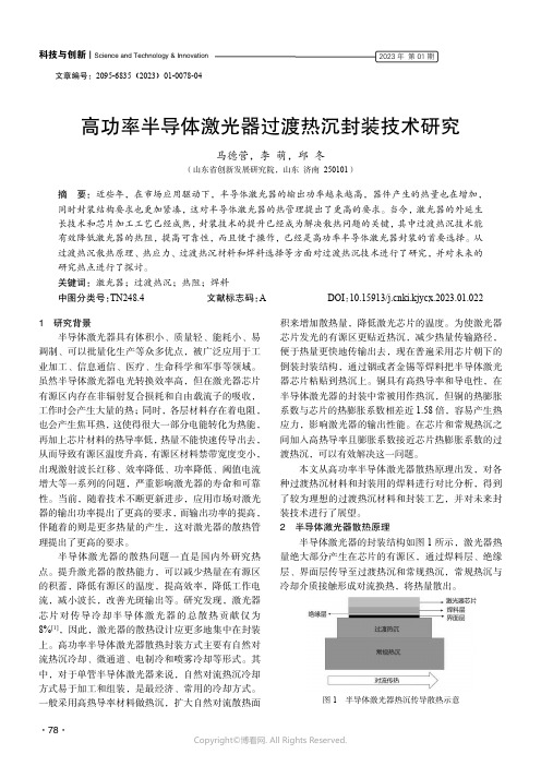
文章编号:2095-6835(2023)01-0078-04高功率半导体激光器过渡热沉封装技术研究马德营,李萌,邱冬(山东省创新发展研究院,山东济南250101)摘要:近些年,在市场应用驱动下,半导体激光器的输出功率越来越高,器件产生的热量也在增加,同时封装结构要求也更加紧凑,这对半导体激光器的热管理提出了更高的要求。
当今,激光器的外延生长技术和芯片加工工艺已经成熟,封装技术的提升已经成为解决散热问题的关键,其中过渡热沉技术能有效降低激光器的热阻,提高可靠性,而且便于操作,已经是高功率半导体激光器封装的首要选择。
从过渡热沉散热原理、热应力、过渡热沉材料和焊料选择等方面对过渡热沉技术进行了研究,并对未来的研究热点进行了探讨。
关键词:激光器;过渡热沉;热阻;焊料中图分类号:TN248.4文献标志码:A DOI:10.15913/ki.kjycx.2023.01.0221研究背景半导体激光器具有体积小、质量轻、能耗小、易调制、可以批量化生产等众多优点,被广泛应用于工业加工、信息通信、医疗、生命科学和军事等领域。
虽然半导体激光器电光转换效率高,但在激光器芯片有源区内存在非辐射复合损耗和自由载流子的吸收,工作时会产生大量的热;同时,各层材料存在着电阻,也会产生焦耳热,这使得很大一部分电能转化为热能,再加上芯片材料的热导率低,热量不能快速传导出去,从而导致有源区温度升高,有源区材料禁带宽度变小,出现激射波长红移、效率降低、功率降低、阈值电流增大等一系列的问题,严重影响激光器的寿命和可靠性。
当前,随着技术不断更新进步,应用市场对激光器的输出功率提出了更高的要求,而输出功率的提高,伴随着的则是更多热量的产生,这对激光器的散热管理提出了更高的要求。
半导体激光器的散热问题一直是国内外研究热点。
提升激光器的散热能力,可以减少热量在有源区的积蓄,降低有源区的温度,提高效率,降低工作电流,减小波长,改善光斑输出等。
研究发现,激光器芯片对传导冷却半导体激光器的总散热贡献仅为8%[1],因此,激光器的散热设计应更多地集中在封装上。
各种封装的Rth热阻参数Thermal-Design

FACTORS AFFECTING Rth(j-a)
There are several factors which affect the characteristic thermal resistance of IC packages. Some of the more significant of these include the test board configuration, the lead frame material, the design of the lead frame and the moulding compound.
Rth(j-a) = Rth(j-c) + Rth(c-a)
Rth(j-c) is the impedance from junction to case (outside surface of package) and Rth(c-a) is the impedance from case to ambient. It is sometimes useful to use only the Rth(c-a) to describe high performance packages where case temperatures are important and externally attached heat radiators may need to be attached. In these cases the overall Rth(j-a) will also include the contribution of the heat radiator.
微电子器件测试与封装-第四章

Page *
内容|半导体器件的测试
8.測試項目(GMP),測試線路如右:
測試方法: GD Short,從DS間灌入一個電流(一般為250uA)量測IDS及VGS,用ID/VGS 得到GFS
GMP:又叫GFS.代表輸入與輸出的關係即GATE 電壓變化,DRAIN電流變化值,單位為S.當汲極電流愈大,GFS也會增大.在切換動作的電路中,GFS值愈高愈好.
VFSD:此為內嵌二極管的正向導通壓降,VFSD=VS-VD
測試目的: 1.檢測晶圓製程中的異常,如背材脫落 2.檢測W/B過程中有無Source wire球脫現象
Remark:Tesec 881中,VFSD+ 可以寫成VGS=0V,VFSD代表G腳Open
Page *
内容|半导体器件的测试
内容|半导体器件测试
热阻测试仪TESEC KT-9614热阻测试仪TESEC KT-9414热阻测试仪EAS测试系统ITC5500 EAS测试系统TESEC 3702LV测试系统觉龙 T331A EAS测试系统SOATESEC SOA测试仪其他DY-2993晶体管筛选仪
内容|半导体器件测试
双极晶体管开关参数测试仪:伏达UI9600 UI9602晶体管测试仪KF-2晶体管测试仪觉龙(绍兴宏邦)晶体管开关参数测试系统肯艺晶体管开关参数测试系统DTS-1000分立器件测试系统MOSFET动态参数测试ITC5900测试系统觉龙 T342栅极等效电阻测试系统
VFVRIR
内容|半导体器件测试
Page *
半导体器件测试的目的:检验产品能否符合技术指标的要求剔除不良品根据参数进行分选可靠性筛选测试内容:静态电参数动态电参数热阻可靠性测试按阶段分芯片测试(中测)成品测试(成测)
- 1、下载文档前请自行甄别文档内容的完整性,平台不提供额外的编辑、内容补充、找答案等附加服务。
- 2、"仅部分预览"的文档,不可在线预览部分如存在完整性等问题,可反馈申请退款(可完整预览的文档不适用该条件!)。
- 3、如文档侵犯您的权益,请联系客服反馈,我们会尽快为您处理(人工客服工作时间:9:00-18:30)。
CHAPTER 6THERMAL DESIGN CONSIDERATIONSpage Introduction 6 - 2 Thermal resistance 6 - 2 Junction temperature 6 - 2 Factors affecting R th(j-a) 6 - 2 Thermal resistance test methods 6 - 3 Test procedure 6 - 3 Forced air factors for thermal resistance 6 - 4 Thermal resistance data - assumptions and precautions 6 - 5 Thermal resistance (R th(j-a)) data 6 - 6 Thermal resistance (R th(j-c)) data tables - power packages 6 - 24INTRODUCTIONThe ability to describe the thermal performance characteristics of a semiconductor IC package is becoming increasingly crucial. With increased power densities,improved reliability and shrinking system sizes, the cooling of IC packages has become a challenging task for design engineers.The situation is further exacerbated by the demand for ever decreasing sizes of electronic devices because, in general, decreasing the size of an electronic package decreases the thermal performance. The designer must carefully balance the benefits of miniaturization and performance against the potential reduction in reliability of electronic components resulting from high operating temperatures.THERMAL RESISTANCEThe ability of a particular semiconductor package to dissipate heat to its environment is expressed in terms of thermal resistance (R th(j-a)). This single entity describes the heat path impedance from the active surface of the semiconductor device (junction) to the ambient operating environment. R th(j-a) can be expressed by its constituents as follows:R th(j-a)=R th(j-c)+R th(c-a)R th(j-c) is the impedance from junction to case (outside surface of package) and R th(c-a) is the impedance from case to ambient. It is sometimes useful to use only theR th(c-a) to describe high performance packages where case temperatures are important and externally attached heat radiators may need to be attached.In these cases the overall R th(j-a)will also include the contribution of the heat radiator.JUNCTION TEMPERATUREWith the R th(j-a) of a package known, the rise in junction temperature (T j) with respect to the ambient temperature (T amb)can be determined at a given power dissipation(P d) of the semiconductor device:T j=(R th(j-a)×P d)+T ambWhere:T j=junction temperature (°C)R th(j-a)=thermal resistance junction to ambient (K/W)P d=power dissipated (W)T amb=ambient temperature (°C)It’s important to note that a lower R th(j-a)indicates a higher thermal performance.FACTORS AFFECTING R th(j-a)There are several factors which affect the characteristic thermal resistance of IC packages. Some of the more significant of these include the test board configuration, the lead frame material, the design of the lead frame and the moulding compound.Test board configurationAn IC package’s thermal resistance highly depends on the Printed Circuit Board (PCB) on which the package is mounted.The copper traces and thermal vias on the PCB provide the major heat dissipation path of the package, therefore the configuration and the size of the copper traces play a significant role in affecting R th(j-a). For test purpose,JEDEC standards(EIA/JEDEC51-3and others) specify two categories of test boards:low effective thermal conductivity test board (low K board) and high effective thermal conductivity test board (high K board). The low K board is a single sided board with only fine signal traces, the high K board is a board with two signal layers and two power (or ground) layers. The real application board is almost always different from the standard test boards, however, the thermal resistance measured from the standard test board provides basic comparable information of the IC package thermal resistance.Lead frame materialThe lead frame material is one of the more important factors in IC package thermal resistance. In early dualin-line packages (DIPs), a Ni/Fe alloy (A42) was the material of choice for lead frames as it provided a good combination of strength and formability as well as assembly process compatibility. However, with the continued miniaturization of IC packages and the need for increased electrical conductivity for advanced ICs, a switch to sophisticated copper alloys was required. Copper alloy lead frames offer several advantages over A42:•they have a high thermal conductivity which reduces thermal resistance, essential for packages such as the Shrink Small Outline Package(SSOP)and Thin Shrink Small Outline Package (TSSOP)•their improved electrical conductivity enhances the electrical performance of a packageMost plastic encapsulated packages produced by Philips Semiconductors incorporate copper alloy lead frames into their design.Lead frame designThe design of a lead frame is another significant contributing factor to thermal resistance. The most important design aspect is the IC attach-pad size and tie bar design. However, the lead frame designer is often faced with fixed parameters such as die size and wire bonding limitations, which reduce lead frame design flexibility.Moulding compoundMoulding compounds also determine IC package thermal resistance. The mould compounds used by Philips Semiconductors are optimized for high purity and quality to provide good thermal performance and reliability.Heat spreadersThe option of a heat spreader, or heat slug, within some packages can improve thermal behaviour by spreading theheat over a larger area of the package, and so improve R th(j-a) or R th(j-c).Adhesive and plating typeOther package related factors include die attach adhesive and lead frame plating type, but the actual influence on thermal resistance is small owing to the fine geometry of these factors.THERMAL RESISTANCE TEST METHODSPhilip Semiconductors uses what is commonly called the Temperature Sensitive Parameter (TSP) method which meets EIA/JEDEC Standards EIA/JESD51-1,EIA/JESD51-2and EIA/JESD51-3.A typical test fixture in still air is shown in Fig.1. The enclosure is a box with an inside dimension of 1 ft3 (0.0283 m3). The enclosure and fixtures are constructed from an insulating material with a low thermal conductance,and all seams thoroughly sealed to ensure there is no airflow through the enclosure.The IC package is then positioned in the geometric center of the enclosure.The forward voltage drop of a calibrated diode incorporated into a special IC is used to correlate a junction temperature change in the IC package to be tested. As the power dissipation is known, the thermal resistance can be calculated using the following equation: Where:R th(j-a)=thermal resistance junction to ambient (K/W)T j=junction temperature (°C)P d=power dissipated (W)T amb=ambient temperature (°C)TEST PROCEDUREThe TSP diode on the semiconductor device is calibrated using a constant temperature oil bath and a constant current power supply(see Fig.2).Calibration temperatures are typically25°C and100°C with a measured accuracy of±0.1°C. The calibration current must be kept low and constant to avoid significant junction heating. The temperature coefficient (K-factor) shown in Fig.3 is calculated using the following equation:Where:K=temperature coefficient (K/mV)T2=high test temperature (°C)T1=low test temperature (°C)V F2=forward voltage at T2 (mV)V F1=forward voltage at T1 (mV)Fig.1 The test fixture in still air.PackageCablesMSC599BoxSubstrateThermocoupleR th j a–()∆T jP d--------T j T amb–()P d----------------------------==KT2T1–()V F2V F1–()-----------------------------=With the K-factor determined,R th(j-a)can be calculated by powering up the device at ambient conditions andmeasuring the forward voltage drop across the TSP diode after temperature equilibrium. Manipulating the original thermal resistance equation with the K-factor,the R th(j-a)of the package can be determined:Fig.2 Test procedure.handbook, halfpage MSB474V FI FD = ON DIE TSPDIODEDOIL BATHMAINTAINED AT CONSTANT TEMPERATUREI = CONSTANTFig.3 V F as a function of T j .handbook, halfpage MSB473V F1V (V)FV F2T 1T 2T ( C)jo R th j a –()∆T j P d --------T j T amb –()P d ----------------------------K V F amb ()V F s ()–()V H I H×------------------------------------------------===Where:V F(amb)=forward voltage of TSP at ambienttemperature (mV)V F(s)=forward voltage of TSP at steady-statetemperature (mV)V H =heating voltage (V)I H =heating current (A)FORCED AIR FACTORS FOR THERMAL RESISTANCE Many applications with ICs have the benefit of forced air cooling by fans or other means.The junction to moving-air thermal resistance can be measured by placing the test setup inside a low velocity wind tunnel (see Fig.4).The test board and device under test are supported with minimal obstruction to the air flow.The average effect of airflow on thermal resistance forpackage types at a particular air flow rate can bedetermined using a “derating” curve (see Fig.5). When using derating curves,it’s important to note that the variety of sizes in a package type group has been averaged.See the following section on “Thermal resistance data -assumptions and precautions” concerning airflow.Fig.4 Wind tunnel - dimensions in cm (inches).MSB475FANTESTPARTANEMOMETERAIR FLOWFLOWSTRAIGHTENER43 (19)35.5(14)58.5 (23)132 (52)183 (72)DIAMETER = 15 (6)not to scaleTHERMAL RESISTANCE DATA -ASSUMPTIONS AND PRECAUTIONSThe graphical data presented in this section are based on measurements ,modelling and estimations . As with all data, some assumptions and contributing factors should be noted:1.The “measured” thermal resistance of an IC packageis highly dependent on the configuration and size of the test board.Data may not be comparable between different semiconductor manufacturers because the test boards may not be the same. Also, the thermal performance of packages for a specific application may be different than presented here because the configuration of the application boards may bedifferent than the test boards.Philips Semiconductors uses low conductive JEDEC test boards for most of the measurements.These low conductive boards are also assumed for modelling.2.Device standoff is a factor in determining thermalresistance especially for surface mounted packages such as SO and QFP packages. The same package from two different manufacturers will often havedifferent standoff from the test boards.In general,high standoff corresponds to a higher thermal resistance.3.The operating environment temperature must be usedas the ambient temperature when calculating junction temperatures in an application. The temperatures inside an electronic enclosure are generally higher than the room temperature.4.When using airflow derating curves (see Fig.5),pleasenote that in actual applications where airflow is available, the flow dynamics may be more complex and turbulent than in a wind tunnel. Also, the many different sizes of packages in a package family such as QFP have been averaged to give one curve for ease-of-use. Lastly, the test boards used in the wind tunnel contribute significantly to forced convection heat transfer and may not be similar to an actual application PC board, especially its size.5.Thermal resistance will vary slightly as a function ofinput power.Generally,as the power input increases,thermal resistance decreases. Thermal resistance changes approximately 5%for a 100%power change.6.Thermal resistance data for some packages were notavailable at the time of publication. Please contact Philips Semiconductors for information on packages not listed in this handbook.7.All data presented are accurate to approximately±15%. For more specific information regarding an application, please contact Philips Semiconductors.8.Philips Semiconductors is also able to providecompact models according to the DELPHI philosophy.In case you need these models or you would like to have more information, please contact theATO-Innovation office in Nijmegen, the Netherlands tel.+31-24-3533085 or fax +31-24-3533350.Fig.5 Average effect of airflow on R th(j-a).handbook, halfpage050−50−40MSC554−30−20−101234air flow (m/s)percent change in R th(j-a) (%)SO SOL SDIPPLCC/QFPDIP LQFPTHERMAL RESISTANCE (R th(j-a)) DATAFig.6 DIP8 (300mil).handbook, halfpage12011010090102030die size (mm 2)R th(j-a)(K/W)MBK303Fig.7 DIP14/16 (300mil).handbook, halfpage10090708060102030die size (mm 2)R th(j-a)(K/W)MBK305Fig.8 DIP18 (300mil).handbook, halfpage90807060102030die size (mm 2)R th(j-a)(K/W)MBK307Fig.9 DIP20 (300mil).handbook, halfpage80706050102030die size (mm 2)R th(j-a)(K/W)MBK304Fig.10 DIP22 (400mil).handbook, halfpage65605550102030die size (mm 2)R th(j-a)(K/W)MBK306Fig.11 DIP24 (300mil).handbook, halfpage7065556050102030die size (mm 2)R th(j-a)(K/W)MBK308Fig.12 DIP24 (400 mil).handbook, halfpage7060504010203040die size (mm 2)R th(j-a)(K/W)MBK309Fig.13 DIP24 (600 mil).handbook, halfpage605550404510203040die size (mm 2)R th(j-a)(K/W)MBK311Fig.14 DIP28 (600 mil).handbook, halfpage555045401020305040die size (mm 2)R th(j-a)(K/W)MBK310Fig.15 DIP40 (600 mil).handbook, halfpage5045403520406080die size (mm 2)R th(j-a)(K/W)MBK312Fig.16 DIP48 (600 mil).handbook, halfpage5045403520406080die size (mm 2)R th(j-a)(K/W)MBK314Fig.17 HSQFP240 (32×32×3.4mm).handbook, halfpage222018161412100300200400500die size (mm 2)R th(j-a)(K/W)MBK319Fig.18 LQFP32 (5×5×1.4mm)handbook, halfpage1009585908051015die size (mm 2)R th(j-a)(K/W)MBK316Fig.19 LQFP32 (7×7×1.4mm).handbook, halfpage10090807060102030die size (mm 2)R th(j-a)(K/W)MBK318Fig.20 LQFP44 (10×10×1.4mm)handbook, halfpage706560555020406080die size (mm 2)R th(j-a)(K/W)MBK320Fig.21 LQFP48 (7×7×1.4mm).handbook, halfpage90708060102030die size (mm 2)R th(j-a)(K/W)MBK321Fig.22 LQFP64 (7×7×1.4mm).handbook, halfpage80757065102030die size (mm 2)R th(j-a)(K/W)MBK323Fig.23 LQFP64 (10×10×1.4mm).handbook, halfpage706560555020604080die size (mm 2)R th(j-a)(K/W)MBK325Fig.24 LQFP80 (12×12×1.4mm).handbook, halfpage6055504520408060die size (mm 2)R th(j-a)(K/W)MBK322Fig.25 LQFP100 (14×14×1.4mm).handbook, halfpage605550454020406080100die size (mm 2)R th(j-a)(K/W)MBK324Fig.26 LQFP128 (14×14×1.4mm).handbook, halfpage605550454020408060100die size (mm 2)R th(j-a)(K/W)MBK326Fig.27 PLCC20 (310mil).handbook, halfpage8270747866102030die size (mm 2)R th(j-a)(K/W)MBK327Fig.28 PLCC28 (410mil).handbook, halfpage8070605010204030die size (mm 2)R th(j-a)(K/W)MBK329Fig.29 PLCC44 (610mil).handbook, halfpage5550454020408010060die size (mm 2)R th(j-a)(K/W)MBK328Fig.30 PLCC52 (710mil).handbook, halfpage555045403520406080100die size (mm 2)R th(j-a)(K/W)MBK330Fig.31 PLCC68 (910mil).handbook, halfpage5048464244404012080160die size (mm 2)R th(j-a)(K/W)MBK332Fig.32 PLCC84 (1110mil).handbook, halfpage42403436383220406080100die size (mm 2)R th(j-a)(K/W)MBK333Fig.33 QFP44 (10×10×1.75mm).handbook, halfpage7570656055501020503040die size (mm 2)R th(j-a)(K/W)MBK335Fig.34 QFP44 FeNi (14×14×2.2mm).handbook, halfpage908070605020604080die size (mm 2)R th(j-a)(K/W)MBK337Fig.35 QFP52 (10×10×2mm).handbook, halfpage7065605545501020304050die size (mm 2)R th(j-a)(K/W)MBK336Fig.36 QFP64 (14×14×2.7mm).handbook, halfpage605550454020604080die size (mm 2)R th(j-a)(K/W)MBK338Fig.37 QFP64 (14×20×2.8mm).handbook, halfpage555040453520406080100die size (mm 2)R th(j-a)(K/W)MBK339Fig.38 QFP80 (14×20×2.8mm).handbook, halfpage55504540354012080die size (mm 2)R th(j-a)(K/W)MBK341Fig.39 QFP100 (14×20×2.8mm).handbook, halfpage52484440368040120die size (mm 2)R th(j-a)(K/W)MBK343Fig.40 QFP120 (28×28×3.4mm).handbook, halfpage40383436324080160120die size (mm 2)R th(j-a)(K/W)MBK340Fig.41 QFP128 (28×28×3.4mm).handbook, halfpage40383634324080120160die size (mm 2)R th(j-a)(K/W)MBK342Fig.42 QFP160 (28×28×3.4mm).handbook, halfpage38363432304012080180160die size (mm 2)R th(j-a)(K/W)MBK344Fig.43 SDIP24 (400mil).handbook, halfpage8070605010203040die size (mm 2)R th(j-a)(K/W)MBK345Fig.44 SDIP32 (400mil).handbook, halfpage7565554510402030die size (mm 2)R th(j-a)(K/W)MBK347Fig.45 SDIP42 (600mil).handbook, halfpage706050403040208060die size (mm 2)R th(j-a)(K/W)MBK349Fig.46 SDIP52 (600mil).handbook, halfpage50453540304080120die size (mm 2)R th(j-a)(K/W)MBK346Fig.47 SDIP64 (750mil).handbook, halfpage4238343020406010080die size (mm 2)R th(j-a)(K/W)MBK348Fig.48 SO8 (150mil).handbook, halfpage162158154150246108die size (mm 2)R th(j-a)(K/W)MBK350Fig.49 SO14 (150mil).handbook, halfpage135125115105210846die size (mm 2)R th(j-a)(K/W)MBK352Fig.50 SO16 (150mil).handbook, halfpage116112108104100421086die size (mm 2)R th(j-a)(K/W)MBK354Fig.51 SO16 (300mil).handbook, halfpage1041009296885102015die size (mm 2)R th(j-a)(K/W)MBK351Fig.52 SO20 (300mil).handbook, halfpage949086825102015die size (mm 2)R th(j-a)(K/W)MBK353Fig.53 SO24 (300mil).handbook, halfpage80767268102030die size (mm 2)R th(j-a)(K/W)MBK355Fig.54 SO28 (300mil).handbook, halfpage7470666210203040die size (mm 2)R th(j-a)(K/W)MBK356Fig.55 SO32 (300mil).handbook, halfpage686664606210403020die size (mm 2)R th(j-a)(K/W)MBK358Fig.56 SSOP14 (5.3mm).handbook, halfpage160155150145140421086die size (mm 2)R th(j-a)(K/W)MBK360Fig.57 SSOP16 (4.4mm).handbook, halfpage160155145150135140241086die size (mm 2)R th(j-a)(K/W)MBK357Fig.58 SSOP16 (5.3mm).handbook, halfpage155145135125241086die size (mm 2)R th(j-a)(K/W)MBK359Fig.59 SSOP20 (4.4mm).handbook, halfpage1501401301204812die size (mm 2)R th(j-a)(K/W)MBK361Fig.60 SSOP20 (5.3mm).handbook, halfpage140130120100110248610die size (mm 2)R th(j-a)(K/W)MBK362Fig.61 SSOP24 (5.3mm).handbook, halfpage130120110901005201510die size (mm 2)R th(j-a)(K/W)MBK364Fig.62 SSOP28 (5.3mm).handbook, halfpage120110100901052015die size (mm 2)R th(j-a)(K/W)MBK366Fig.63 SSOP56 (7.5mm).handbook, halfpage838482818051510die size (mm 2)R th(j-a)(K/W)MBK365Fig.64 TQFP44 (10×10×1mm).handbook, halfpage757060655520408060die size (mm 2)R th(j-a)(K/W)MBK367Fig.65 TQFP64 (10×10×1mm).handbook, halfpage75706550556020406080die size (mm 2)R th(j-a)(K/W)MBK368Fig.66 TQFP80 (12×12×1mm).handbook, halfpage6560555020806040die size (mm 2)R th(j-a)(K/W)MBK370Fig.67 TQFP100 (14×14×1mm).handbook, halfpage6055504540208060die size (mm 2)R th(j-a)(K/W)MBK372Fig.68 TSSOP14 (4.4mm).handbook, halfpage1801701501602486die size (mm 2)R th(j-a)(K/W)MBK369Fig.69 TSSOP16 (4.4mm).handbook, halfpage1601651551501401452864die size (mm 2)R th(j-a)(K/W)MBK371Fig.70 TSSOP20 (4.4mm).handbook, halfpage150145135140130241086die size (mm 2)R th(j-a)(K/W)MBK373Fig.71 TSSOP24 (4.4mm).handbook, halfpage136132128120124246108die size (mm 2)R th(j-a)(K/W)MBK374Fig.72 TSSOP28 (4.4mm).handbook, halfpage130125120115210864die size (mm 2)R th(j-a)(K/W)MBK376Fig.73 TSSOP48 (6.1mm).handbook, halfpage106104100102988412die size (mm 2)R th(j-a)(K/W)MBK378Fig.74 TSSOP56 (6.1mm).handbook, halfpage98969092944128die size (mm 2)R th(j-a)(K/W)MBK375Fig.75 VSO40 FeNi (7.5mm).handbook, halfpage12512011511010403020die size (mm 2)R th(j-a)(K/W)MBK377Fig.76 VSO56 FeNi (11mm).handbook, halfpage1081041009610204030die size (mm 2)R th(j-a)(K/W)MBK379THERMAL RESISTANCE (R th(j-c)) DATA TABLES - POWER PACKAGES(1)PACKAGE NAME PHILIPS OUTLINE CODE R th(j-c) (K/W) GLUED DIE R th(j-c) (K/W) SOLDERED DIE DBS9MPF SOT111-1 6.0to12.0n.a.DBS9P SOT157-2 1.0to4.00.8to3.0DBS13P SOT141-6 1.0to4.00.8to3.0DBS17P SOT243-1 1.0to4.00.8to3.0DBS23P SOT411-1n.a.0.8to3.0HSOP20SOT418-2 1.0to4.00.8to3.0RBS9MPF SOT352-1 6.0to12.0n.a.RDBS13P SOT462-1 1.0to4.00.8to3.0SIL9MPF SOT110-1 6.0to12.0n.a.SIL9P SOT131-2 1.0to4.00.8to3.0SIL13P SOT193-2 1.0to4.00.8to3.0Note1.a)Almost all of the values in the table were determined with measurements.b)Low values should be used with a large die, high values should be used with a small die.。