单片机外文翻译
单片机-外文翻译-外文文献-英文文献-单片机简介-中英对照电子教案

Single chip brief introductionThe monolithic integrated circuit said that the monolithic micro controller, it is not completes some logical function the chip, but integrates a computer system to a chip on. Summary speaking: A chip has become a computer. Its volume is small, the quality is light, and the price cheap, for the study, the application and the development has provided the convenient condition. At the same time, the study use monolithic integrated circuit is understandsthe computer principle and the structure best choice.The monolithic integrated circuit interior also uses with the computer function similar module, for instance CPU, memory, parallel main line, but also has with the hard disk behave identically the memory component7 what is different is its these part performance is opposite our home-use computer weak many, but the price is also low, generally does not surpass 10 Yuan then Made some control electric appliance one kind with it is not the 'very complex work foot, We use now the completely automatic drum washer, the platoon petti-coat pipe: VCD and so on Inside the electrical appliances may see its form! It is mainly takes the control section the core part.It is one kind of online -like real-time control computer, online -like is the scene control, needs to have the strong antijamming ability, the low cost, this is also and the off-line type computer (forinstance home use PC,) main differenceThe monolithic integrated circuit is depending on the procedure, and may revise. Realizes the different function through the different procedure, particularly special unique some functions, this is other component needs to take the very big effort to be able to achieve, some are the flowered big strength is also very difficult to achieve. One is not the very complex function, if develops in the 50s with the US 74 series, or the 60s's CD4000 series these pure hardware do decides, the electric circuit certainly arc a big PCB board ! But if, if succeededin the 70s with the US puts in the market the series monolithic integrated circuit, the result will have the huge difference. Because only the monolithic integrated circuit compiles through you the procedure may realize the high intelligence, high efficiency, as well as redundant reliabilityThe CPU is the key component of a digital computer. Its purpose is to decode instruction received from memory and perform transfers, arithmetic, logic, and control operations with data stored in internal registers, memory, or I/O interface units. Externally, the CPU provides one or more buses for transferring instructions, data, and control information to and from components connected to it. A microcontroller is present in the keyboard and in the monitor in the generic computer; thus these components are also shaded. In such microcontrollers, the CPU may be quite different from those discussed in this chapter. The word lengths may be short, the number of registers small, and the instruction sets limited. Performance, relatively speaking, is poor, but adequate for the task. Most important, the cost of these microcontrollers is very low, making their use cost effective.Because the monolithic integrated circuit to the cost is sensitive, therefore present occupies the dominant status the software is the most preliminary assembly language7 it was except the binary machine code above the most preliminary language, since why were such preliminary must use?Why high-level did the language already achieve the visualization programming level not to use? The reason is very simple, is the monolithic integrated circuit docs not have home computer such CPU, and also has not looked like the hard disk such mass memory equipment. Inside even if a visualization higher order language compilation script only then a button, also will achieve several dozens K the sizes! Does not speak anything regarding the home use PC hard disk, but says regarding the monolithic integrated circuit cannot accept. The monolithic integrated circuit in the hardware source aspect's use factor must very Gao Caixing, therefore assembly, although primitive actually massively is using, Same truth, if attains supercomputer'son operating system and the application software home use PC to come up the movement, home use PC could also not withstand.It can be said that the 20th century surmounted three "the electricity" the time, namely the electrical time, the Electronic Age and already entered computer time. However, this kind of computer, usually refers to the personal computer, is called PC machine. It by the main engine, the keyboard, the monitor and so on is composed. Also has a kind of computer, most people actually not how familiar. This kind of computeris entrusts with the intelligence each kind of mechanical monolithic integrated circuit (also to call micro controller). , This kind of computer's smallest system only has used as the name suggests a piece of integrated circuit, then carries on the simple operation and the control. Because its volume is small, usually hides in is accused the machinery "the belly". It in the entire installment, plays is having like the human brains role, it went wrong, the entire installment paralyzed. Now, this kind of monolithic integrated circuit's use domain already very widespread, like the intelligent measuring appliance, the solid work paid by time control, the communication equipment, the guidance system, the domestic electric appliances and so on, Once each product used the monolithic integrated circuit, could get up causes theeffect which the product turned to a new generation, often before product range crown by adjective ‘ intelligence ' , like intelligence washer and so on. Nowsome factory's technical personnel or other extra-curricular electronic exploiter do certain products, are not the electric circuit are too complex, is the function is too simple, and is imitated extremely easily. Investigates its reason, possibly on card, in the product has not used on the monolithic integrated circuit or other programmable logical component.单片机简介单片机又称单片微控制器,它不是完成某一个逻辑功能的芯片,而是把一个计算机系统集成到一个芯片上。
单片机 外文翻译 外文文献 英文文献 单片机简介 中英对
单片机外文翻译外文文献英文文献单片机简介中英对原文来源图书馆电子资源Single chip brief introductionThe monolithic integrated circuit said that the monolithic micro controller, it is not completes some logical function the chip, but integrates a computer system to a chip on. Summary speaking: A chip has become a computer. Its volume is small, the quality is light, and the price cheap, for the study, the application and the development has provided the convenient condition. At the same time, the study use monolithic integrated circuit is understands the computer principle and the structure best choice.The monolithic integrated circuit interior also uses with the computer function similar module, for instance CPU, memory, parallel main line, but also has with the hard disk behave identically the memory component7 what is different is its these part performance is opposite our home-use computer weak many, but the price is also low, generally does not surpass 10 Yuan then Made some control electric appliance one kind with it is not the 'very complex work foot, We use now the completely automatic drum washer, the platoon petti-coat pipe: VCD and so on Inside the electrical appliances may see its form! It is mainly takes the control section the core part.It is one kind of online -like real-time control computer, online -like is the scene control, needs to have the strong antijamming ability,the low cost, this is also and the off-line type computer (for instance home use PC,) main differenceThe monolithic integrated circuit is depending on the procedure, and may revise. Realizes the different function through the different procedure, particularly special unique some functions, this is other component needs to take the very big effort to be able to achieve, some are the flowered big strength is also very difficult to achieve. One is not the very complex function, if develops in the 50s with the US 74 series, or the 60s's CD4000 series these pure hardware do decides, the electric circuit certainly arc a big PCB board ! But if, if succeeded in the 70s with the US puts in the market the series monolithic integrated circuit, the result will have the huge difference. Because only the monolithic integrated circuit compiles through you the procedure may realize the high intelligence, high efficiency, as well as redundant reliabilityThe CPU is the key component of a digital computer. Its purpose isto decode instruction received from memory and perform transfers, arithmetic, logic, and control operations with data stored in internal registers, memory, or I/O interface units. Externally, the CPU provides one or more buses for transferring instructions, data, and control information to and from components connected to it. A microcontroller is present in the keyboard and in the monitor in the generic computer; thus these components are also shaded. In such microcontrollers, the CPU may be quite different from those discussed in this chapter. The wordlengths may be short, the number of registers small, and the instruction sets limited. Performance, relatively speaking, is poor, but adequatefor the task. Most important, the cost of these microcontrollers is very low, making their use cost effective.Because the monolithic integrated circuit to the cost is sensitive, therefore present occupies the dominant status the software is the most preliminary assembly language7 it was except the binary machine code above the most preliminary language, sincewhy were such preliminary must use?Why high-level did the language already achieve the visualization programming level not to use? The reason is very simple, is the monolithic integrated circuit docs not have home computer such CPU, and also has not looked like the hard disk such mass memory equipment. Inside even if a visualization higher order language compilation script only then a button, also will achieve several dozens K the sizes! Does not speak anything regarding the home use PC hard disk, but says regarding the monolithic integrated circuit cannot accept. The monolithic integrated circuit in the hardware source aspect's use factor must very Gao Caixing, therefore assembly, although primitive actually massively is using, Same truth, if attains supercomputer's on operating system and the application software home use PC to come up the movement, home use PC could also not withstand.It can be said that the 20th century surmounted three "the electricity" the time, namely the electrical time, the Electronic Ageand already entered computer time. However, this kind of computer, usually refers to the personal computer, is called PC machine. It by the main engine, the keyboard, the monitor and so on is composed. Also has a kind of computer, most people actually not how familiar. This kind of computer is entrusts with the intelligence each kind of mechanical monolithic integrated circuit (also to call micro controller). , This kind of computer's smallest system only has used as the name suggests a piece of integrated circuit, then carries on the simple operation and the control. Because its volume is small, usually hides in is accused the machinery "the belly". It in the entire installment, plays is having like the human brains role, it went wrong, the entire installment paralyzed. Now, this kind of monolithic integrated circuit's use domain already very widespread, like the intelligent measuring appliance, the solid work paid by time control, the communication equipment, the guidance system, the domestic electric appliances and so on, Once each product used the monolithic integrated circuit, could get up causes the effect which the product turned to a new generation, often before product range crown by adjective---- …intelligence?, like intelligence washer and so on. Now some factory's technical personnel or other extra-curricular electronic exploiter do certain products, are not theelectric circuit are too complex, is the function is too simple, and is imitated extremely easily. Investigates its reason, possibly on card, in the product has not used on the monolithic integrated circuit or other programmable logical component.单片机简介单片机又称单片微控制器,它不是完成某一个逻辑功能的芯片,而是把一个计算机系统集成到一个芯片上。
单片机英文文献资料及翻译

单片机英文文献资料及翻译单片机(英文:Microcontroller)Microcontroller is a small computer on a single integrated circuit that contains a processor core, memory, and programmable input/output peripherals. Microcontrollers are designed for embedded applications, in contrast to the microprocessors used in personal computers or other general purpose applications.A microcontroller's processor core is typically a small, low-power computer dedicated to controlling the operation of the device in which it is embedded. It is often designed to provide efficient and reliable control of simple and repetitive tasks, such as switching on and off lights, or monitoring temperature or pressure sensors.MEMORYMicrocontrollers typically have a limited amount of memory, divided into program memory and data memory. The program memory is where the software that controls the device is stored, and is often a type of Read-Only Memory (ROM). The data memory, on the other hand, is used to store data that is used by the program, and is often volatile, meaning that it loses its contents when power is removed.INPUT/OUTPUTMicrocontrollers typically have a number of programmable input/output (I/O) pins that can be used to interface with external sensors, switches, actuators, and other devices. These pins can be programmed to perform specific functions,such as reading a sensor value, controlling a motor, or generating a signal. Many microcontrollers also support communication protocols like serial, parallel, and USB, allowing them to interface with other devices, including other microcontrollers, computers, and smartphones.APPLICATIONSMicrocontrollers are widely used in a variety of applications, including:- Home automation systems- Automotive electronics- Medical devices- Industrial control systems- Consumer electronics- RoboticsCONCLUSIONIn conclusion, microcontrollers are powerful and versatile devices that have become an essential component in many embedded systems. With their small size, low power consumption, and high level of integration, microcontrollers offer an effective and cost-efficient solution for controlling a wide range of devices and applications.。
单片机基础外文翻译参考文献

单片机基础外文翻译参考文献(文档含中英文对照即英文原文和中文翻译)原文:Fundamentals of Single-chip MicrocomputerDr. Dobbs MacintoshJournalAbstractT h e s i n gl e-chi p m i c r o com pu t er i s t h e cul m i na t i on of bo t h t h e d e v el opm e nt o f t h e di gi t al c om p ut e r a nd t h e i nt e gra t e d c i r c ui t a rgu a b l y t h e t ow m o s t s i gn i fi c ant i nv en t i on s of t h e 20t h ce n t u r y .T h es e t o w t yp e s o f a rc hi t e c t u r e a r e fo un d i n s i n gl e-c hi pm i c r o com pu t e r.S om e e m p l o y t h e s pl i t p ro gr a m/d at a m em o r y o f t h e H a r v a rd a r ch i t e ct u r e, s ho wn i n F i g.3-5A-1, ot h er s f o l l o w t h e p hi l o so ph y,w i d e l y a d a p t ed f o r ge n e r al-pu rp os e com p ut e rs an d m i c r op r oc e s s o rs,of m ak i n g n o l o gi c al di s t i nc t i on be t w ee n p ro gr a m a n d d at a m em o r y a s i n t h e P r i n c et on ar c hi t e ct u r e.In ge n e r a l t er m s a si n gl e-c hi p m i cro c om put e r i s c ha r ac t e ri z ed b y t h e i n co r po r at i o n o f al l t h e u ni t s o f a c om put e r i n t o a s i n gl e d e vi c e.Keyword: Single-chip Microcomputer ROM RAM Programming Algorithm Features• Compatible with MCS-51™ Products• 4K Bytes of In-System Reprogrammable Flash Memory– Endurance: 1,000 Write/Erase Cycles• Fully Static Operation: 0 Hz to 24 MHz• Three-level Program Memory Lock• 128 x 8-bit Internal RAM• 32 Programmable I/O Lines• Two 16-bit Timer/Counters• Six Interrupt Sources• Programmable Serial Channel• Low-power Idle and Power-down ModesDescriptionThe AT89C51 is a low-power, high-performance CMOS 8-bit microcomputer with 4Kbytes of Flash programmable and erasable read only memory (PEROM). The deviceis manufactured using Atmel’s high-density nonvolatile memory technology and iscompatible with the industry-standard MCS-51 instruction set and pinout. Theon-chipFlash allows the program memory to be reprogrammed in-system or by a conventionalnonvolatile memory programmer. By combining a versatile 8-bit CPU with Flashon a monolithic chip, the Atmel AT89C51 is a powerful microcomputer which providesa highly-flexible and cost-effective solution to many embedded controlapplications.The AT89C51 provides the following standard features: 4Kbytes of Flash, 128 bytes of RAM, 32 I/O lines, two 16-bittimer/counters, a five vector two-level interrupt architecture,a full duplex serial port, on-chip oscillator and clock circuitry.In addition, the AT89C51 is designed with static logicfor operation down to zero frequency and supports twosoftware selectable power saving modes. The Idle Modestops the CPU while allowing the RAM, timer/counters,serial port and interrupt system to continue functioning. ThePower-down Mode saves the RAM contents but freezesthe oscillator disabling all other chip functions until the nexthardware reset.Pin ConfigurationsBlock DiagramPin DescriptionVCCSupply voltage.GNDGround.Port 0Port 0 is an 8-bit open-drain bi-directional I/O port. As anoutput port, each pin can sink eight TTL inputs. When 1sare written to port 0 pins, the pins can be used as highimpedanceinputs.Port 0 may also be configured to be the multiplexed loworderaddress/data bus during accesses to external programand data memory. In this mode P0 has internalpullups.Port 0 also receives the code bytes during Flash programming,and outputs the code bytes during programverification. External pullups are required during program verification.Port 1Port 1 is an 8-bit bi-directional I/O port with internal pullups.The Port 1 output buffers can sink/source four TTL inputs.When 1s are written to Port 1 pins they are pulled high bythe internal pullups and can be used as inputs. As inputs,Port 1 pins that are externally being pulled low will source current (IIL) because of the internal pullups.Port 1 also receives the low-order address bytes during Flash programming and verification.Port 2Port 2 is an 8-bit bi-directional I/O port with internal pullups.The Port 2 output buffers can sink/source four TTL inputs.When 1s are written to Port 2 pins they are pulled high by the internal pullups and can be used as inputs. As inputs, Port 2 pins that are externally being pulled low will source current (IIL) because of the internal pullups.Port 2 emits the high-order address byte during fetches from external program memory and during accesses to external data memory that use 16-bit addresses (MOVX @DPTR). In this application, it uses strong internal pullups when emitting 1s. During accesses to external data memory that use 8-bit addresses (MOVX @ RI), Port 2 emits the contents of the P2 Special Function Register.Port 2 also receives the high-orderaddress bits and some control signals during Flash programming and verification.Port 3Port 3 is an 8-bit bi-directional I/O port with internal pullups.The Port 3 output buffers can sink/source four TTL inputs.When 1s are written to Port 3 pins they are pulled high by the internal pullups and can be used as inputs. As inputs,Port 3 pins that are externally being pulled low will source current (IIL) because of the pullups.Port 3 also serves the functions of various special features of the AT89C51 as listed below:Port 3 also receives some control signals for Flash programmingand verification.ALE/PROGAddress Latch Enable output pulse for latching the low byte of the address during accesses to external memory. This pin is also the program pulse input (PROG) during Flash programming.In normal operation ALE is emitted at a constant rate of 1/6the oscillator frequency, and may be used for external timing or clocking purposes. Note, however, that one ALE pulse is skipped during each access to external Data Memory.If desired, ALE operation can be disabled by setting bit 0 of SFR location 8EH. With the bit set, ALE is active only during a MOVX or MOVC instruction. Otherwise, the pin is weakly pulled high. Setting the ALE-disable bit has no effect if the microcontroller is in external execution mode.PSENProgram Store Enable is the read strobe to external program memory.When theAT89C51 is executing code from external programmemory, PSEN is activated twice each machine cycle, except that two PSEN activations are skipped during each access to external data memory.EA/VPPExternal Access Enable. EA must be strapped to GND in order to enable the device to fetch code from external program memory locations starting at 0000H up to FFFFH.Note, however, that if lock bit 1 is programmed, EA will be internally latched on reset. EA should be strapped to VCC for internal program executions. This pin also receives the 12-volt programming enable voltage (VPP) during Flash programming, for parts that require 12-volt VPP.XTAL1Input to the inverting oscillator amplifier and input to the internal clock operating circuit.XTAL2Output from the inverting oscillator amplifier.Oscillator CharacteristicsXTAL1 and XTAL2 are the input and output, respectively,of an inverting amplifier which can be configured for use as an on-chip oscillator, as shown in Figure 1. Either a quartz crystal or ceramic resonator may be used. To drive the device from an external clock source, XTAL2 should be left unconnected while XTAL1 is driven as shown in Figure 2. There are no requirements on the duty cycle of the external clock signal, since the input to the internal clocking circuitry is through a divide-by-two flip-flop, but minimum and maximum voltage high and low time specifications must be observed.Idle ModeIn idle mode, the CPU puts itself to sleep while all the onchip peripherals remain active. The mode is invoked by software. The content of the on-chip RAM and all the special functions registers remain unchanged during this mode. The idle mode can be terminated by any enabled interrupt or by a hardware reset. It should be noted that when idle is terminated by a hard ware reset, the device normally resumes programexecution,from where it left off, up to two machine cycles before the internal reset algorithm takes control. On-chip hardware inhibits access to internal RAM in this event, but access to the port pins is not inhibited. To eliminate the possibility of an unexpected write to a port pin when Idle is terminated by reset, the instruction following the one that invokes Idle should not be one that writes to a port pin or to external memory.Figure 1. Oscillator ConnectionsFigure 2. External Clock Drive ConfigurationPower-down ModeIn the power-down mode, the oscillator is stopped, and the instruction that invokes power-down is the last instruction executed. The on-chip RAM and Special Function Registers retain their values until the power-down mode is terminated. The only exit from power-down is a hardware reset. Reset redefines the SFRs but does not change the on-chip RAM. The reset should not be activated before VCC is restored to its normal operating level and must be held active long enough to allow the oscillator to restart and stabilize.Program Memory Lock BitsOn the chip are three lock bits which can be left unprogrammed (U) or can be programmed (P) to obtain the additional features listed in the table below.When lock bit 1 is programmed, the logic level at the EA pin is sampled and latched during reset. If the device is powered up without a reset, the latch initializes to a random value, and holds that value until reset is activated. It is necessary that the latched value of EA be in agreement with the current logic level at that pin in order for the device to function properly.Programming the FlashThe AT89C51 is normally shipped with the on-chip Flash memory array in the erased state (that is, contents = FFH) and ready to be programmed. The programming interface accepts either a high-voltage (12-volt) or a low-voltage (VCC) program enable signal. The low-voltage programming mode provides a convenient way to program theAT89C51 inside the user’s system, while the high-voltage programming mode is compatible with conventional thirdparty Flash or EPROM programmers. The AT89C51 is shipped with either the high-voltage or low-voltage programming mode enabled. The respective top-side marking and device signature codes are listed in the following table.The AT89C51 code memory array is programmed byte-bybyte in either programming mode. To program any nonblank byte in the on-chip Flash Memory, the entire memory must be erased using the Chip Erase Mode.Programming Algorithm: Before programming the AT89C51, the address, data and control signals should be set up according to the Flash programming mode table and Figure 3 and Figure 4. To program the AT89C51, take the following steps.1. Input the desired memory location on the address lines.2. Input the appropriate data byte on the data lines.3. Activate the correct combination of control signals.4. Raise EA/VPP to 12V for the high-voltage programming mode.5. Pulse ALE/PROG once to program a byte in the Flash array or the lock bits. The byte-write cycle is self-timed and typically takes no more than 1.5 ms.Repeat steps 1 through 5, changing the address and data for the entire array or until the end of the object file is reached.Data Polling: The AT89C51 features Data Polling to indicate the end of a write cycle. During a write cycle, an attempted read of the last byte written will result in the complement of the written datum on PO.7. Once the write cycle has been completed, true data are valid on all outputs, and the next cycle may begin. Data Polling may begin any time after a write cycle has been initiated.Ready/Busy: The progress of byte programming can also be monitored by theRDY/BSY output signal. P3.4 is pulled low after ALE goes high during programming to indicate BUSY. P3.4 is pulled high again when programming is done to indicate READY.Program Verify: If lock bits LB1 and LB2 have not been programmed, the programmed code data can be read back via the address and data lines for verification. The lock bits cannot be verified directly. Verification of the lock bits is achieved by observing that their features are enabled.Chip Erase: The entire Flash array is erased electrically by using the proper combination of control signals and by holding ALE/PROG low for 10 ms. The code array is written with all “1”s. The chip erase operatio n must be executed before the code memory can be re-programmed.Reading the Signature Bytes: The signature bytes are read by the same procedure as a normal verification of locations 030H, 031H, and 032H, except that P3.6 and P3.7 must be pulled to a logic low. The values returned are as follows.(030H) = 1EH indicates manufactured by Atmel(031H) = 51H indicates 89C51(032H) = FFH indicates 12V programming(032H) = 05H indicates 5V programmingProgramming InterfaceEvery code byte in the Flash array can be written and the entire array can be erasedby using the appropriate combination of control signals. The write operation cycle is selftimed and once initiated, will automatically time itself to completion. All major programming vendors offer worldwide support for the Atmel microcontroller series. Please contact your local programming vendor for the appropriate software revision.译文:单片机基础摘要:单片机是电脑和集成电路发展的巅峰,有据可查的是它们也是20世纪最意义的两大发明。
单片机外文翻译--8位8字节闪存单片机AT89C52
电子与信息工程学院本科毕业论文(设计)外文文献翻译译文题目: 8-bit Microcontroller With 8K Bytes Flash AT89C52 学生姓名:专业:电气工程及其自动化指导教师:2012年11月外文资料8-bit Microcontroller With 8K Bytes Flash AT89C52FeaturesCompatible with MCS-51™ Products8K Bytes of In-System Reprogrammable Flash MemoryEndurance: 1,000 Write/Erase CyclesFully Static Operation: 0 Hz to 24 MHzThree-level Program Memory Lock256 x 8-bit Internal RAM32 Programmable I/O LinesThree 16-bit Timer/CountersEight Interrupt SourcesProgrammable Serial ChannelLow-power Idle and Power-down ModesDescriptionThe AT89C52 is a low-power, high-performance CMOS 8-bit microcomputer with 8K bytes of Flash programmable and erasable read only memory (PEROM). The device is manufactured using Atmel’s high-density nonvolatile memory technology and is compatible with the industry-standard 80C51 and 80C52 instruction set and pin out. The on-chip Flash allows the program memory to be reprogrammed in-system or by a conventional nonvolatile memory programmer. By combining a versatile 8-bit CPU with Flash on a monolithic chip, the Atmel AT89C52 is a powerful microcomputer which provides a highly-flexible and cost-effective solution to many embedded control applications.Pin ConfigurationsBlock DiagramPin DescriptionVCCSupply voltage.GNDGround.Port 0Port 0 is an 8-bit open drain bi-directional I/O port. As an output port, each pin can sink eight TTL inputs. When 1s are written to port 0 pins, the pins can be used as high-impedance inputs. Port 0 can also be configured to be the multiplexed low-order address/data bus during accesses to external program and data memory. In this mode, P0 has internal pull-ups. Port 0 also receives the code bytes during Flash programming and outputs the code bytes during program verification. External pull-ups are required during program verification.Port 1Port 1 is an 8-bit bi-directional I/O port with internal pull-ups. The Port 1 output buffers can sink/source four TTL inputs. When 1s are written to Port 1 pins, they are pulled high by the internal pull-ups and can be used as inputs. As inputs, Port 1 pins that are externally being pulled low will source current (I IL) because of the internal pull-ups. In addition, P1.0 and P1.1 can be configured to be the timer/counter 2 external count input (P1.0/T2) and the timer/counter 2 trigger input (P1.1/T2EX), respectively, as shown in the following table. Port 1 also receives the low-order address bytes during Flash programming and verification.Port 2Port 2 is an 8-bit bi-directional I/O port with internal pull-ups. The Port 2 outputbuffers can sink/source four TTL inputs. When 1s are written to Port 2 pins, they are pulled high by the internal pull-ups and can be used as inputs. As inputs, Port 2 pins that are externally being pulled low will source current (I IL) because of the internal pull-ups. Port 2 emits the high-order address byte during fetches from external program memory and during accesses to external data memories that use 16-bit addresses (MOVX @DPTR). In this application, Port 2 uses strong internal pull-ups when emitting 1s. During accesses to external data memories that use 8-bit addresses (MOVX @ RI), Port 2 emits the contents of the P2 Special Function Register. Port 2 also receives the high-order address bits and some control signals during Flash programming and verification.Port 3Port 3 is an 8-bit bi-directional I/O port with internal pull-ups. The Port 3 output buffers can sink/source four TTL inputs. When 1s are written to Port 3 pins, they are pulled high by the internal pull-ups and can be used as inputs. As inputs, Port 3 pins that are externally being pulled low will source current (I IL) because of the pull-ups. Port 3 also serves the functions of various special features of the AT89C51, as shown in the following table. Port 3 also receives some control signals for Flash programming and verification.RSTReset input. A high on this pin for two machine cycles while the oscillator is running resets the device.ALE/PROGAddress Latch Enable is an output pulse for latching the low byte of the address during accesses to external memory. This pin is also the program pulse input (PROG) during Flash programming. In normal operation, ALE is emitted at a constant rate of 1/6 the oscillator frequency and may be used for external timing or clocking purposes. Note, however, that one ALE pulse is skipped during each access to external data memory. If desired, ALE operation can be disabled by setting bit 0 of SFR location 8EH. With the bit set, ALE is active only during a MOVX or MOVC instruction. Otherwise, the pin is weakly pulled high. Setting the ALE-disable bit has no effect if the microcontroller is in external execution mode.PSENProgram Store Enable is the read strobe to external program memory. When the AT89C52 is executing code from external program memory, PSEN is activated twice each machine cycle, except that two PSEN activations are skipped during each access to external data memory.EA/VPPExternal Access Enable. EA must be strapped to GND in order to enable the device to fetch code from external program memory locations starting at 0000H up to FFFFH. Note, however, that if lock bit 1 is programmed, EA will be internally latched on reset. EA should be strapped to V CC for internal program executions. This pin also receives the 12-volt programming enable voltage (V PP) during Flash programming when 12-volt programming is selected.XTAL1Input to the inverting oscillator amplifier and input to the internal clock operating circuit.XTAL2Output from the inverting oscillator amplifier.Special Function RegistersA map of the on-chip memory area called the Special Function Register (SFR) space is shown in the Table 1.Note that not all of the addresses are occupied, and unoccupied addresses may not be implemented on the chip. Read accesses to these addresses will in general return random data, and write accesses will have an indeterminate effect. User software should not write 1s to these unlisted locations, since they may be used in future products to invoke new features. In that case, the reset or inactive values of the new bits will always be 0.Timer 2 RegistersControl and status bits are contained in registers T2CON and T2MOD for Timer 2. The register pair (RCAP2H, RCAP2L) are the Capture/Reload registers for Timer 2in 16-bit capture mode or 16-bit auto-reload mode.Interrupt RegistersThe individual interrupt enable bits are in the IE register. Two priorities can be set for each of the six interrupt sources in the IP register.Data MemoryThe AT89C52 implements 256 bytes of on-chip RAM. The upper 128 bytes occupy a parallel address space to the Special Function Registers. That means the upper 128 bytes have the same addresses as the SFR space but are physically separate from SFR space.When an instruction accesses an internal location above address 7FH, the address mode used in the instruction specifies whether the CPU accesses the upper 128 bytes of RAM or the SFR space. Instructions that use direct addressing access SFR space. For example, the following direct addressing instruction accesses the SFR at location 0A0H .MOV 0A0H, #dataInstructions that use indirect addressing access the upper 128 bytes of RAM. For example, the following indirect addressing instruction, where R0 contains 0A0H, accesses the data byte at address 0A0H, rather than P2 (whose address is 0A0H).MOV @R0, #dataNote that stack operations are examples of indirect addressing, so the upper 128 bytes of data RAM are available as stack space.Timer 0 and 1Timer 0 and Timer 1 in the AT89C52 operate the same way as Timer 0 and Timer 1 in the AT89C51.Timer 2 is a 16-bit Timer/Counter that can operate as either a timer or an event counter. The type of operation is selected by bit C/T2 in the SFR T2CON.Timer 2 has three operating modes: capture, auto-reload (up or down counting), and baud rate generator. The modes are selected by bits in T2CON, as shown in Table 3.Timer 2 consists of two 8-bit registers, TH2 and TL2. In the Timer function, the TL2 register is incremented every machine cycle. Since a machine cycle consists of 12 oscillator periods, the count rate is 1/12 of the oscillator frequency.In the Counter function, the register is incremented in response to a 1-to-0 transition at its corresponding external input pin, T2. In this function, the external input is sampled during S5P2 of every machine cycle. When the samples show a high in one cycle and a low in the next cycle, the count is incremented. The new count value appears in the register during S3P1 of the cycle following the one in which the transition was detected. Since two machine cycles (24 oscillator periods) are required to recognize a 1-to-0 transition, the maximum count rate is 1/24 of the oscillator frequency. To ensure that a given level is sampled at least once before it changes, the level should be held for at least one full machine cycle.Capture ModeIn the capture mode, two options are selected by bit EXEN2 in T2CON. If EXEN2 = 0, Timer 2 is a 16-bit timer or counter which upon overflow sets bit TF2 in T2CON.This bit can then be used to generate an interrupt. If EXEN2 = 1, Timer 2 performs the same operation, but a 1-to-0 transition at external input T2EX also causes the current value in TH2 and TL2 to be captured into RCAP2H and RCAP2L, respectively. In addition, the transition at T2EX causes bit EXF2 in T2CON to be set. The EXF2 bit, like TF2 can generate an interrupt. The capture mode is illustrated inAuto-reload (Up or Down Counter)Timer 2 can be programmed to count up or down when configured in its 16-bit auto-reload mode. This feature is invoked by the DCEN (Down Counter Enable) bit located in the SFR T2MOD. Upon reset, the DCEN bit is set to 0 so that timer 2 will default to count up. When DCEN is set, Timer 2 can count up or down, depending on the value of the T2EX pin.Figure 2 shows Timer 2 automatically counting up when DCEN = 0. In this mode, two options are selected by bit EXEN2 in T2CON. If EXEN2 = 0, Timer 2 counts up to 0FFFFH and then sets the TF2 bit upon overflow. The overflow also causes the timer registers to be reloaded with the 16-bit value in RCAP2H and RCAP2L. The values in Timer in Capture ModeRCAP2H and RCAP2L are preset by software. If EXEN2 = 1, a 16-bit reload can be triggered either by an overflow or by a 1-to-0 transition at external input T2EX. This transition also sets the EXF2 bit. Both the TF2 and EXF2 bits can generate an interrupt if enabled.Setting the DCEN bit enables Timer 2 to count up or down, as shown in Figure 3. In this mode, the T2EX pin controls the direction of the count. A logic 1 at T2EX makes Timer 2 count up. The timer will overflow at 0FFFFH and set the TF2 bit. This overflow also causes the 16-bit value in RCAP2H and RCAP2L to be reloaded into the timer registers, TH2 and TL2, respectively.A logic 0 at T2EX makes Timer 2 count down. The timer underflows when TH2 and TL2 equal the values stored in RCAP2H and RCAP2L. The underflow sets the TF2 bit and causes 0FFFFH to be reloaded into the timer registers. The EXF2 bit toggles whenever Timer 2 overflows or underflows and can be used as a 17th bit of resolution. In this operating mode, EXF2 does not flag an interrupt.外文资料译文:8位8字节闪存单片机AT89C52主要性能●与MCS-51单片机产品兼容●8K字节在系统可编程Flash存储器●1000次擦写周期●全静态操作:0Hz~24Hz●三级加密程序存储器●256×8位内部存储器●32个可编程I/O口线●三个16位定时器/计数器●八个中断源●可编程串行通道●低功耗空闲和掉电模式功能特性描述AT89S52是一种低功耗、高性能CMOS8位微控制器,具有8K内置可编程闪存。
(完整版)MCS-51系列单片机中英文资料对照外文翻译文献综述
MCS-51系列单片机中英文资料对照外文翻译文献综述Structure and function of the MCS-51 seriesStructure and function of the MCS-51 series one-chip computer MCS-51 is a name of a piece of one-chip computer series which Intel Company produces. This company introduced 8 top-grade one-chip computers of MCS-51 series in 1980 after introducing 8 one-chip computers of MCS-48 series in 1976. It belong to a lot of kinds this line of one-chip computer the chips have, such as 8051, 8031, 8751, 80C51BH, 80C31BH,etc., their basic composition, basic performance and instruction system are all the same.8051 daily representatives-51 serial one-chip computers.A one-chip computer system is made up of several following parts: (1) One microprocessor of 8 (CPU). ( 2) At slice data memory RAM (128B/256B),it use not depositing not can reading /data that write, such as result not middle of operation, final result and data wanted to show, etc. (3) Procedure memory ROM/EPROM (4KB/8KB ), is used to preserve theprocedure , some initial data and form in slice. But does not take ROM/EPROM within some one-chip computers, such as 8031, 8032.(4) Four 8 run side by side I/O interface P0 four P3, each mouth can use as introduction , may use as exporting too. (5) Two timer / counter, each timer / counter may set up and count in the way, used to count to the external incident, can set up into a timing way too, and can according to count or result of timing realize the control of the computer. (6) Five cut off cutting off the control system of the source. (7) One all duplex serial I/O mouth of UART (universal asynchronous receiver/transmitter (UART) ), is it realize one-chip computer or one-chip computer and serial communication of computer to use for. (8) Stretch oscillator and clock produce circuit, quartz crystal finely tune electric capacity need outer. Allow oscillation frequency as 12 megahertz now at most. Every the above-mentioned part was joined through the inside data bus .Among them, CPU is a core of the one-chip computer, it is the control of the computer and command centre, made up of such parts as arithmetic unit and controller , etc.. The arithmetic unit can carry on 8 persons of arithmetic operation and unit ALU of logic operation while including one, the 1 storing device temporaries of 8, storing device 2 temporarily, 8's accumulation device ACC, register B and procedure state register PSW, etc. Person who accumulate ACC count by 2 input ends entered of checking etc. temporarily as one operation often, come from person who store 1 operation is it is it make operation to go on to count temporarily , operation result and loop back ACC with another one. Inaddition, ACC is often regarded as the transfer station of data transmission on 8051 inside. The same as general microprocessor, it is the busiest register. Help remembering that agreeing with a express in the order. The controller includes the procedure counter, the order is deposited, the order deciphering, the oscillator and timing circuit, etc. The procedure counter is made up of counter of 8 for two, amounts to 16. It is a byte address counter of the procedure in fact, the content is the next IA that will carried out in PC. The content which changes it can change the direction that the procedure carries out. Shake the circuit in 8051 one-chip computers, only need outer quartz crystal and frequency to finely tune the electric capacity, its frequency range is its 12MHZ of 1.2MHZ. This pulse signal, as 8051 basic beats of working, namely the minimum unit of time. 8051 is the same as other computers, the work in harmony under the control of the basic beat, just like an orchestra according to the beat play that is commanded.There are ROM (procedure memory , can only read ) and RAM in 8051 slices (data memory, can is it can write ) two to read, they have each independent memory address space, dispose way to be the same with general memory of computer. Procedure 8051 memory and 8751 slice procedure memory capacity 4KB, address begin from 0000H, used for preserving the procedure and form constant. Data 8051- 8751 8031 of memory data memory 128B, address false 00FH, using for middle result to deposit operation, the data are stored temporarily and the data are buffered. In RAM of this 128B, there is unit of 32 bytes that can be appointed as the jobregister, this and general microprocessor is different, 8051 slice RAM and job register rank one formation the same to arrange the location. It is not very the same that the memory of MCS-51 series one-chip computer and general computer disposes the way in addition. General computer for first address space, ROM and RAM can arrange in different space within the range of this address at will, namely the addresses of ROM and RAM, with distributing different address space in a formation. While visiting the memory, corresponding and only an address Memory unit, can ROM, it can be RAM too, and by visiting the order similarly. This kind of memory structure is called the structure of Princeton. 8051 memories are divided into procedure memory space and data memory space on the physics structure, there are four memory spaces in all: The procedure stores in one and data memory space outside data memory and one in procedure memory space and one outside one, the structure forms of this kind of procedure device and data memory separated form data memory, called Harvard structure. But use the angle from users, 8051 memory address space is divided into three kinds: (1) In the slice, arrange blocks of FFFFH, 0000H of location, in unison outside the slice (use 16 addresses). (2) The data memory address space outside one of 64KB, the address is arranged from 0000H 64KB FFFFH (with 16 addresses) too to the location. (3) Data memory address space of 256B (use 8 addresses). Three above-mentioned memory space addresses overlap, for distinguishing and designing the order symbol of different data transmission in the instruction system of 8051: CPU visit slice, ROM orderspend MOVC , visit block RAM order uses MOVX outside the slice, RAM order uses MOV to visit in slice.8051 one-chip computer have four 8 walk abreast I/O ports, call P0, P1, P2 and P3. Each port is 8 accurate two-way mouths, accounts for 32 pins altogether. Every one I/O line can be used as introduction and exported independently. Each port includes a latch (namely special function register), one exports the driver and a introduction buffer. Make data can latch when outputting, data can buffer when making introduction, but four function of pass away these self-same. Expand among the system of memory outside having slice, four ports these may serve as accurate two-way mouth of I/O in common use. Expand among the system of memory outside having slice, P2 mouth see high 8 address off; P0 mouth is a two-way bus, send the introduction of 8 low addresses and data / export in timesharing The circuit of 8051 one-chip computers and four I/O ports is very ingenious in design. Familiar with I/O port logical circuit, not only help to use port correctly and rationally, and will inspire to designing the peripheral logical circuit of one-chip computer to some extent. Load ability and interface of port have certain requirement, because output grade, P0 of mouth and P1 end output, P3 of mouth grade different at structure, so, the load ability and interface of its door demand to have nothing in common with each other. P0 mouth is different from other mouth, its output grade draws the resistance supremely. When using it as the mouth in common use, output grade is it leak circuit to turn on, is it urge NMOS draw the resistanceon taking to be outer with it while inputting to go out to fail. When being used as introduction, should write"1" to a latch first. Every one with P0 mouth can drive 8 Model LS TTL load to export. P1 mouth is an accurate two-way mouth too, used as I/O in common use. Different from P0 mouth output of circuit its, draw load resistance link with power on inside have. In fact, the resistance is that two effects are in charge of FET and together: One FET is in charge of load, its resistance is regular. Another one can is it lead to work with close at two state, make its President resistance value change approximate 0 or group value heavy two situation very. When it is 0 that the resistance is approximate, can draw the pin to the high level fast; when resistance value is very large, P1 mouth high electricity at ordinary times, can is it draw electric current load to offer outwards, draw electric current load to offer outwards, draw the resistance on needn't answer and thinking. Here when the port is used as introduction, must write into 1 to the corresponding latch first too, make FET end relatively about 20,000 ohms because of load resistance in scene and because 40,000 ohms, will not exert an influence on the data that are input. The structure of P2 some mouth is similar to P0 mouth, there are MUX switches. Is it similar to mouth partly to urge, but mouth large a conversion controls some than P1.P3 mouth one multi-functional port, mouth getting many than P1 it have "3 doors and 4 buffers". Two parts there, make her besides accurate two-way function with P1 mouth just, can also use the second function of every pin, "and" door 3 functions one switch in fact, it determines to be to output data of latch tooutput second signal of function. Act as W=At 1 o'clock, output Q end signal; act as Q=At 1 o'clock, can output W line signal. At the time of programming, it is that the first function is still the second function but needn't have software that set up P3 mouth in advance .It hardware not inside is the automatic to have two function outputted when CPU carries on SFR and seeks the location to visit to P3 mouth/at not lasting lining, there are inside hardware latch Qs=1. The operation principle of P3 mouth is similar to P1 mouth.Output grade, P3 of mouth, P1 of P1, connect with inside have load resistance of drawing, every one of they can drive 4 Model LS TTL load to output. As while inputting the mouth, any TTL or NMOS circuit can drive P1 of 8051 one-chip computers as P3 mouth in a normal way. Because draw resistance on output grade of them have, can open a way collector too or drain-source resistance is it urge to open a way, do not need to have the resistance of drawing outer. Mouths are all accurate two-way mouths too. When the conduct is input, must write the corresponding port latch with 1 first. As to 80C51 one-chip computer, port can only offer milliampere of output electric currents, is it output mouth go when urging one ordinary basing of transistor to regard as, should contact a resistance among the port and transistor base, in order to the electricity while restraining the high level from exporting P1~P3 Being restored to the throne is the operation of initializing of an one-chip computer. Its main function is to turn PC into 0000H initially, make the one-chip computer begin to hold the conductprocedure from unit 0000H. Except that the ones that enter the system are initialized normally, as because procedure operate it make mistakes or operate there aren't mistake, in order to extricate oneself from a predicament , need to be pressed and restored to the throne the key restarting too. It is an input end which is restored to the throne the signal in 8051 China RST pin. Restore to the throne signal high level effective, should sustain 24 shake cycle (namely 2 machine cycles) the above its effective times. If 6 of frequency of utilization brilliant to shake, restore to the throne signal duration should exceed 4 delicate to finish restoring to the throne and operating. Produce the logic picture of circuit which is restored to the throne the signal: restore to the throne the circuit and include two parts outside in the chip entirely. Outside that circuit produce to restore to the throne signal (RST) hand over to Schmitt's trigger, restore to the throne circuit sample to output , Schmitt of trigger constantly in each S5P2 , machine of cycle in having one more , then just got and restored to the throne and operated the necessary signal inside. Restore to the throne resistance of circuit generally, electric capacity parameter suitable for 6 brilliant to shake, can is it restore to the throne signal high level duration greater than 2 machine cycles to guarantee. Being restored to the throne in the circuit is simple, its function is very important. Pieces of one-chip computer system could normal running, should first check it can restore to the throne not succeeding. Checking and can pop one's head and monitor the pin with the oscilloscope tentatively, push and is restored to the throne the key, the wave form that observes andhas enough range is exported (instantaneous), can also through is it restore to the throne circuit group holding value carry on the experiment to change.MCS-51系列单片机的功能和结构MSC-51系列单片机具有一个单芯片电脑的结构和功能,它是英特尔公司的系列产品的名称。
单片机外文翻译
Electric boiler temperature system1.MCUA microcontroller (or MCU) is a computer-on-a-chip. It is a type of microprocessor emphasizing self-sufficiency and cost-effectiveness, in contrast to a general-purpose microprocessor (the kind used in a PC).The majority of computer systems in use today are embedded in other machinery, such as telephones, clocks, appliances, vehicles, and infrastructure. An embedded system usually has minimal requirements for memory and program length and may require simple but unusual input/output systems. For example, most embedded systems lack keyboards, screens, disks, printers, or other recognizable I/O devices of a personal computer. They may control electric motors, relays or voltages, and read switches, variable resistors or other electronic devices. Often, the only I/O device readable by a human is a single light-emitting diode, and severe cost or power constraints can even eliminate that.In contrast to general-purpose CPUs, microcontrollers do not have an address bus or a data bus, because they integrate all the RAM and non-volatile memory on the same chip as the CPU. Because they need fewer pins, the chip can be placed in a much smaller, cheaper package.Integrating the memory and other peripherals on a single chip and testing them as a unit increases the cost of that chip, but often results in decreased net cost of the embedded system as a whole. (Even if the cost of a CPU that has integrated peripherals is slightly more than the cost of a CPU + external peripherals, having fewer chips typically allows a smaller and cheaper circuit board, and reduces the labor required to assemble and test the circuit board). This trend leads to design.A microcontroller is a single integrated circuit, commonly with the following features:central processing unit - ranging from small and simple 4-bit processors to sophisticated 32- or 64-bit processorsinput/output interfaces such as serial ports (UARTs)other serial communications interfaces like I²C, Serial Peripheral Interface and Controller Area Network for system interconnect peripherals such as timers and watchdog RAM for data storage ROM, EPROM,EEPROM or Flash memory for program storage clock generator - often an oscillator for a quartz timing crystal, resonator or RC circuit many include analog-to-digital converters .This integration drastically reduces the number of chips and the amount of wiring and PCB space that would be needed to produce equivalent systems using separate chips and have proved to be highly popular in embedded systems since their introduction in the 1970s.Some microcontrollers can afford to use a Harvard architecture: separate memory buses for instructions and data, allowing accesses to take place concurrently.The decision of which peripheral to integrate is often difficult. The Microcontroller vendors often trade operating frequencies and system design flexibility against time-to-market requirements from their customers and overall lower system cost. Manufacturers have to balance the need to minimize the chip size against additional functionality.Microcontroller architectures are available from many different vendors in so many varieties that each instruction set architecture could rightly belong to a category of their own. Chief among these are the 8051, Z80 and ARM derivatives.[citation needed]A microcontroller (also MCU or µC) is a functio nal computer system-on-a-chip. It contains a processor core, memory, and programmable input/output peripherals.Microcontrollers include an integrated CPU, memory (a small amount of RAM, program memory, or both) and peripherals capable of input and output.It emphasizes high integration, in contrast to a microprocessor which only contains a CPU (the kind used in a PC). In addition to the usual arithmetic and logic elements of a general purpose microprocessor, the microcontroller integrates additional elements such as read-write memory for data storage, read-only memory for program storage, Flash memory for permanent data storage, peripherals, and input/output interfaces. At clock speeds of as little as 32KHz, microcontrollers often operate at very low speed compared to microprocessors, but this is adequate for typical applications. They consume relatively little power (milliwatts or even microwatts), and will generally have the ability to retain functionality while waiting for an event such as a button press or interrupt. Power consumption while sleeping (CPU clock and peripherals disabled) may be just nanowatts, making them ideal for low power and long lasting battery applications.Microcontrollers are used in automatically controlled products and devices, such as automobile engine control systems, remote controls,office machines, appliances, power tools, and toys. By reducing the size, cost, and power consumption compared to a design using a separate microprocessor, memory, and input/output devices, microcontrollers make it economical to electronically control many more processes.The majority of computer systems in use today are embedded in other machinery, such as automobiles, telephones, appliances, and peripherals for computer systems. These are called embedded systems. While some embedded systems are very sophisticated, many have minimal requirements for memory and program length, with no operating system, and low software complexity. Typical input and output devices include switches, relays, solenoids, LEDs, small or custom LCD displays, radio frequency devices, and sensors for data such as temperature, humidity, light level etc. Embedded systems usually have no keyboard, screen, disks, printers, or other recognizable I/O devices of a personal computer, and may lack human interaction devices of any kind.It is mandatory that microcontrollers provide real time response to events in the embedded system they are controlling. When certain events occur, an interrupt system can signal the processor to suspend processing the current instruction sequence and to begin an interrupt service routine (ISR). The ISR will perform any processing required based on the source of the interrupt before returning to the original instruction sequence. Possible interrupt sources are device dependent, and often include events such as an internal timer overflow, completing an analog to digital conversion, a logic level change on an input such as from a button being pressed, and data received on a communication link. Where power consumption is important as in battery operated devices, interrupts may also wake a microcontroller from a low power sleep state where the processor is halted until required to do something by a peripheral event.Microcontroller programs must fit in the available on-chip program memory, since it would be costly to provide a system with external, expandable, memory. Compilers and assembly language are used to turn high-level language programs into a compact machine code for storage in the microcontroller's memory. Depending on the device, the program memory may be permanent, read-only memory that can only be programmed at the factory, or program memory may be field-alterable flash or erasable read-only memory.Since embedded processors are usually used to control devices, they sometimes need to accept input from the device they are controlling. This is the purpose of the analog to digital converter. Since processors are built to interpret and process digital data, i.e. 1s and 0s, they won'tbe able to do anything with the analog signals that may be being sent to it by a device. So the analog to digital converter is used to convert the incoming data into a form that the processor can recognize. There is also a digital to analog converter that allows the processor to send data to the device it is controlling.In addition to the converters, many embedded microprocessors include a variety of timers as well. One of the most common types of timers is the Programmable Interval Timer, or PIT for short. A PIT just counts down from some value to zero. Once it reaches zero, it sends an interrupt to the processor indicating that it has finished counting. This is useful for devices such as thermostats, which periodically test the temperature around them to see if they need to turn the air conditioner on, the heater on, etc.Time Processing Unit or TPU for short. Is essentially just another timer, but more sophisticated. In addition to counting down, the TPU can detect input events, generate output events, and other useful operations.Dedicated Pulse Width Modulation (PWM) block makes it possible for the CPU to control power converters, resistive loads, motors, etc., without using lots of CPU resources in tight timer loops.Universal Asynchronous Receiver/Transmitter (UART) block makes it possible to receive and transmit data over a serial line with very little load on the CPU.For those wanting ethernet one can use an external chip like Crystal Semiconductor CS8900A, Realtek RTL8019, or Microchip ENC 28J60. All of them allow easy interfacing with low pin count.DescriptionThe AT89C51 is a low-power, high-performance CMOS 8-bit microcomputer with 4K bytes of Flash programmable and erasable read only memory (PEROM). The device is manufactured using Atmel’s high-density nonvolatile memory technology and is compatible with the industry-standard MCS-51 instruction set and pinout. The on-chip Flash allows the program memory to be reprogrammed in-system or by a conventional nonvolatile memory programmer. By combining a versatile 8-bit CPU with Flash on a monolithic chip, the Atmel AT89C51 is a powerful microcomputer which provides a highly-flexible and cost-effective solution to many embedded control applications.Function characteristicThe AT89C51 provides the following standard features: 4K bytes of Flash, 128 bytes of RAM, 32 I/O lines, two 16-bit timer/counters, a five vector two-level interrupt architecture, a full duplex serial port, on-chip oscillator and clock circuitry. In addition, the AT89C51 is designed with static logic for operation down to zero frequency and supports two software selectable power saving modes. The Idle Mode stops the CPU while allowing the RAM, timer/counters, serial port and interrupt system to continue functioning. The Power-down Mode saves the RAM contents but freezes the oscillator disabling all other chip functions until the next hardware reset.Pin DescriptionVCC:Supply voltage.GND:Ground.Port 0Port 0 is an 8-bit open-drain bi-directional I/O port. As an output port, each pin can sink eight TTL inputs. When 1s are written to port 0 pins, the pins can be used as highimpedance inputs.Port 0 may also be configured to be the multiplexed loworder address/data bus during accesses to external program and data memory. In this mode P0 has internal pullups.Port 0 also receives the code bytes during Flash programming,and outputs the code bytes during programverification. External pullups are required during programverification.Port 1Port 1 is an 8-bit bi-directional I/O port with internal pullups.The Port 1 output buffers can sink/source four TTL inputs.When 1s are written to Port 1 pins they are pulled high by the internal pullups and can be used as inputs. As inputs,Port 1 pins that are externally being pulled low will source current (IIL) because of the internal pullups.Port 1 also receives the low-order address bytes during Flash programming and verification.Port 2Port 2 is an 8-bit bi-directional I/O port with internal pullups.The Port 2 output buffers can sink/source four TTL inputs.When 1s are written to Port 2 pins they are pulled high by the internal pullups and can beused as inputs. As inputs,Port 2 pins that are externally being pulled low will source current, because of the internal pullups.Port 2 emits the high-order address byte during fetches from external program memory and during accesses to external data memory that use 16-bit addresses. In this application, it uses strong internal pullupswhen emitting 1s. During accesses to external data memory that use 8-bit addresses, Port 2 emits the contents of the P2 Special Function Register.Port 2 also receives the high-order address bits and some control signals during Flash programming and verification.Port 3Port 3 is an 8-bit bi-directional I/O port with internal pullups.The Port 3 output buffers can sink/source four TTL inputs.When 1s are written to Port 3 pins they are pulled high by the internal pullups and can be used as inputs. As inputs,Port 3 pins that are externally being pulled low will source current (IIL) because of the pullups.Port 3 also serves the functions of various special features of the AT89C51 as listed below:Port 3 also receives some control signals for Flash programming and verification.RSTReset input. A high on this pin for two machine cycles while the oscillator is running resets the device.ALE/PROGAddress Latch Enable output pulse for latching the low byte of the address during accesses to external memory. This pin is also the program pulse input (PROG) during Flash programming.In normal operation ALE isemitted at a constant rate of 1/6 the oscillator frequency, and may be used for external timing or clocking purposes. Note, however, that one ALE pulse is skipped during each access to external Data Memory.If desired, ALE operation can be disabled by setting bit 0 of SFR location 8EH. With the bit set, ALE is active only during a MOVX or MOVC instruction. Otherwise, the pin is weakly pulled high. Setting the ALE-disable bit has no effect if the microcontroller is in external execution mode.PSENProgram Store Enable is the read strobe to external program memory.When the AT89C51 is executing code from external program memory, PSEN is activated twice each machine cycle, except that two PSEN activations are skipped during each access to external data memory.EA/VPPExternal Access Enable. EA must be strapped to GND in order to enable the device to fetch code from external program memory locations starting at 0000H up to FFFFH. Note, however, that if lock bit 1 is programmed, EA will be internally latched on reset.EA should be strapped to VCC for internal program executions.This pin also receives the 12-volt programming enable voltage(VPP) during Flash programming, for parts that require12-volt VPP.XTAL1Input to the inverting oscillator amplifier and input to the internal clock operating circuit.XTAL2Output from the inverting oscillator amplifier.Oscillator CharacteristicsXTAL1 and XTAL2 are the input and output, respectively,of an inverting amplifier which can be configured for use as an on-chip oscillator, as shown in Figure 1.Either a quartz crystal or ceramic resonator may be used. To drive the device from an external clock source, XTAL2 should be left unconnected while XTAL1 is driven as shown in Figure 2.There are no requirements on the duty cycle of the external clock signal, since the input to the internal clocking circuitry is through a divide-by-two flip-flop, but minimum and maximum voltage high and low timespecifications must be observed.Figure 1. Oscillator Connections Figure 2. External Clock Drive ConfigurationIdle ModeIn idle mode, the CPU puts itself to sleep while all the onchip peripherals remain active. The mode is invoked by software. The content of the on-chip RAM and all the special functions registers remain unchanged during this mode. The idle mode can be terminated by any enabled interrupt or by a hardware reset.It should be noted that when idle is terminated by a hard ware reset, the device normally resumes program execution,from where it left off, up to two machine cycles before the internal reset algorithm takes control. On-chip hardware inhibits access to internal RAM in this event, but access to the port pins is not inhibited. To eliminate the possibility of an unexpected write to a port pin when Idle is terminated by reset, the instruction following the one that invokes Idle should not be one that writes to a port pin or to external memory.Power-down ModeIn the power-down mode, the oscillator is stopped, and the instruction that invokes power-down is the last instruction executed. The on-chip RAM and Special Function Registers retain their values until the power-down mode is terminated. The only exit from power-down is a hardware reset. Reset redefines the SFRs but does not change the on-chip RAM. The reset should not be activated before VCC is restored to its normal operating level and must be held active long enough to allow the oscillator to restart and stabilize.Program Memory Lock BitsOn the chip are three lock bits which can be left unprogrammed (U) or can be programmed (P) to obtain the additional features listed in the table below.When lock bit 1 is programmed, the logic level at the EA pin is sampled and latched during reset. If the device is powered up without a reset, the latch initializes to a random value, and holds that value until reset is activated. It is necessary that the latched value of EA be in agreement with the current logic level at that pin in order for the device to function properly.中文翻译:1.单片机单片机即单片微型计算机,是把中央处理器、存储器、定时/计数器、输入输出接口都集成在一块集成电路芯片上的微型计算机。
单片机的外文文献及中文翻译
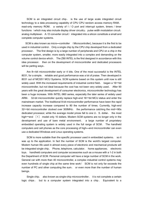
SCM is an integrated circuit chip,is the use of large scale integrated circuit technology to a data processing capability of CPU CPU random access memory RAM,read-only memory ROM,a variety of I / O port and interrupt system, timers / timer functions (which may also include display driver circuitry,pulse width modulation circuit,analog multiplexer,A / D converter circuit)integrated into a silicon constitute a small and complete computer systems.SCM is also known as micro—controller (Microcontroller), because it is the first to be used in industrial control。
Only a single chip by the CPU chip developed from a dedicated processor。
The first design is by a large number of peripherals and CPU on a chip in the computer system, smaller, more easily integrated into a complex and demanding on the volume control device which。
- 1、下载文档前请自行甄别文档内容的完整性,平台不提供额外的编辑、内容补充、找答案等附加服务。
- 2、"仅部分预览"的文档,不可在线预览部分如存在完整性等问题,可反馈申请退款(可完整预览的文档不适用该条件!)。
- 3、如文档侵犯您的权益,请联系客服反馈,我们会尽快为您处理(人工客服工作时间:9:00-18:30)。
外文资料翻译STC89C52 processing chipPrime features:With MCS - 51 SCM product compatibility, 8K bytes in the systemprogrammable Flash memory, 1000 times CaXie cycle, the static operation: 0Hz ~ 33Hz, triple enc ryption program memory, 32 programmed I/O port, three 16 timer/counter, the eight uninterrupt ed dual-career UART serial passage, low power consumption, leisure and fall after fall electric po wer mode can be awakened and continuous watchdog timer and double-number pointer, power i dentifier. Efficacy: characteristicsSTC89C52 is one kind of low power consumption, high CMOS8 bitmicro-controller, 8K in system programmable Flash memory. Use high-density nonvolatile storage technology, and industrial 80C51 product instruction and pin fully compatible. The Flash memory chips allows programs in the system, also suitable for programmable conventional programming. In a single chip, have clever 8 bits CPU and online system programmable Flash, increase STC89C5 2 for many embedded control system to provide high vigorous application and useful solutions. S TC89C52 has following standard efficacy: 8k byte Flash RAM, 256 bytes, 32 I/O port, the watchdo g timer, two, three pointer numerical 16 timer/counter, a 6 vector level 2 continuous structure, th e serial port, working within crystals and horological circuit. In addition, 0Hz AT89S52 can drop to the static logic operation, support two software can choose power saving mode. Idle mode, the C PU to stop working, and allows the RAM, timer/counters, serial, continuous to work. Protection a sana pattern, RAM content is survival, vibrators frozen, SCM, until all the work under a continuou s or hardware reset. 8-bit microcontrollers 8K bytes in the system programmable Flash AT89S52 d evices.Mouth: P0 P0 mouth is a two-way open drain I/O. As export, each candrive eight TTL logic level. For P0 port to write "1", foot as the highimpedance input.When access to external programs and numerical memory, also knownas low P0 mouth eight address/numerical reuse. In this mode, with the internal P0 resistor.In the flash when programming, also used for P0 mouth; absorbinstruction bytes In the process, the output command byte calibration. When the program requir es external, calibration on pull-up resistors.Mouth: P1 mouth P1 is an internal resistance of the eight two-way I/Obuffers can drive, P1 output four TTL logic level. To write "1" P1 port, the internal resistance to po rt, can push as input mouth. When used as input, external and internal foot because of low resist ance, will output current (IIL).In addition, P1.0 and P1.2 respectively timer/counter 2 externalcounting input (P1.0 / T2) and when the trigger editor/counter P1.1 input (2), specific T2EX/are s hown below. In programming and calibration, flash P1 mouth absorb eight address low byte. Effic acy: the foot.P1.0 T2 (timer/counter T2 external counting input), clock outputP1.1 T2EX (timer/counter T2 capture/overloaded triggered signals anddirection control),P1.5 MOSI (with) online system programming,P1.6 MISO (with) online system programming,P1.7 SCK (with) online system programming,Mouth: P2 P2 mouth is an internal resistance of the eight two-way I/Obuffers and P2 output can drive four TTL logic level. To write "1" P2 port, the internal resistance t o port, can push as input mouth. When used as input, external and internal foot because of low r esistance, will output current (IIL).In the external program memory access or use 16bit external numericalmemory address read (for example MOVX execution DPTR @), P2 mouth send out high 8 address . In this application, P2 mouth on the internal use strong pull send 1. In using 8-bit address (such as MOVX @ RI) access to external numerical memory, P2 mouth output P2 latches content. In pro gramming and calibration, flash P2 mouth also absorb high eight address byte and some control s ignal.P3: a P3 mouth on the inside of the eight two-way pull-up resistorsI/O buffers can drive, p2 output four TTL logic level. For P3 port to write "1", the internal resistanc e to port, can push as input mouth. When used as input, external and internal foot because of lo w resistance, will output current (IIL). P3 mouth AT89S52 special functions (also as the second effi cacy), are shown below. In programming and calibration, flash also absorb some P3 mouth contro l signals.Port pin second efficacy:P3.0 RXD (serial input)P3.1 TXD (serial export),P3.2 INTO the discontinuous (0) P3.3 INT1 (1) the discontinuousP3.4 (time/counter TO 0)P3.5 T1 (1) time/counter,P3.6 WR (external numerical memory write for)P3.7 RD (external numerical memory read for)In addition, also absorb some used in mp3 mouth FLASH memoryprogramming and calibration of program control signals.RST, reset input: when the vibrator, RST pin appeared two machinecycle above high level will be reset the chip.ALE/PROG - when access to external program memory or numericalmemory, ALE (address latch allow) output pulses are used to latch address of low eight bytes. Nor mally, ALE with clock frequencies are 1/6 output pulse signal with fixed, so it can be used for the purpose or output clocks. Timing Those who want an attention is: whenever access to external n umerical memory will skip a ALE pulse.For FLASH memory programming, this pin is used for inputprogramming pulse (.) PROGIf necessary, but through special effect to the zone registers (SFR) 8EH D0 position, the unit ca n be banned ALE operations. This position is a bit, MOVX and MOVC instructions will be activated . ALE -- In addition, the foot will be weak, execute external program MCU hign should be banned, a void. Set ALEPSEN - program storage PSEN allowed (output is outside of theprogram memory read, choose communication by external program memory when taking AT89C 52 instructions (or), each machine cycle PSEN twice, two pulse output is useful, during this period, when access to external numerical memory, will skip PSEN twice.EA/VPP - external access permission, to make the CPU only access toexternal program memory (address for 0000H - FFFFH), EA end must remain low level (ground). S hould notice is: if a LB1 is encrypted, reset when programming will latch EA end.As for the high level of the EA (VCCS), the CPU is theimplementation of the program memory internal instructions.FLASH memory when programming, this pin plus + 12 v programming allow power Vpp, of cour se, that is the part is used to Vpp voltage 12V programming.中文翻译STC89C52处理芯片首要性能:与MCS-51单片机产物兼容、8K字节在系统可编程Flash存储器、 1000次擦写周期、全静态操作:0Hz~33Hz 、三级加密程序存储器、 32个可编程I/O口线、三个16位定时器/计数器八个间断源、全双职工UART串行通道、低功耗空闲和掉电模式、掉电后间断可唤醒、看门狗定时器、双数值指针、掉电标识符。