富士通单片机MB90F927数据手册
f2mc-8fx 家族mb95200h210h 系列如何进行cr 调节

序程节调 数的外以 ,
动启将器配适 确正的 确正的
。后电上 标目在生发程过节调 。变改了生发率 频钟时 果如率频钟时 节调要需且,态状的钟时 解了需器配适 ,前始开试调 。止终试调 ,开断会将信通的器配适 与 标目, ± 围范下以出超率频钟时 若 。率频 的 于基是置设的率 特波。信通 线单持支以号信率特波的 生产于用被器荡振 ,下式模试调 。率频 制控以器存寄制控 节调过通能功节调 的器配适 。理原节调 绍介章本
CRTH [4:0] [4:0] CRTH [4:0] CRTL [4:0]
// set CRTH & CRTL 6
CR MHz (
和
的中区
了改修户用若。区
。 至变改能 , 置设码代户用下如像若 。区留预是 和 的区存闪 。复恢够能值些这后位复,值 至存并出取区存闪自据数的 ,时位复
NVR
I/O
置配的器存寄
2.3-1: NVR
器荡振 主 章 第 作操节调
CR
CR 2
V1.0
图
I/O
CRTH
CRTL
改修可户用但
。信通线单保确可度精该。 ± 至节调 把是法做种这,下况情常通。 示指 对将其, 到收接 标目自器配适 若,间期节调 。 作用 回返器配适 向会后节调做稍 标目 ,令命节调的确正到收接若;值的 和 加增性硬会 标目,后之误 错收接令命次每。令命节调待等始开并, 置 和 使 标目 。节调 始开 标目,后误错桢次多生发令命节调的到收接。令命节调到收地确正 接能不 标目则。率频 的误错到得 标目后电上,坏破被 的中 标目若 。 败失节调 限界出超间时试重或 标目向续持 会器配适 ,时节调 行进
SmartPRO编程器编程Spansion的MCU产品应用手册说明书
广州致远电子股份有限公司文件信息类别内容关键词SmartPRO 通用编程器 Spansion FUJITSU MCU摘要本文介绍如何使用SmartPRO 系列通用编程器来编程Spansion 的MCU 芯片。
SmartPRO 编程器编程Spansion 的MCU修订历史版本日期原因V1.00 2008/09/01 创建文档。
V1.01 2009/10/10 将文档中图片修改为SmartPRO 2008版软件截图V1.02 2014/07/23 更改半导体公司名称、修改错别字目录1.Spansion的MCU芯片支持情况 (1)2.Spansion的MCU芯片特点 (2)2.1 加密特点 (2)2.2 NVR区 (2)3.应用软件界面简介 (3)4.烧录器件的步骤 (4)4.1 选择器件 (4)4.2 将数据装入缓冲区 (5)4.3 设置芯片配置信息及加密选项 (6)4.4 编程芯片 (6)4.5 组合定制 (7)4.6 量产 (7)5.脱机模式 (9)5.1 脱机操作说明 (9)5.1.1 键盘使用规则 (9)5.1.2 菜单介绍 (9)5.1.3 创建脱机工程 (9)1.制作脱机工程 (9)2.填写工程信息 (10)3.选择存储介质 (10)5.2 脱机操作步骤 (10)6.免责声明 (13)1. Spansion的MCU芯片支持情况目前,在SmartPRO 5000U-Plus和SmartPRO T9000-PLUS 编程器上均支持52种Spansion(原FUJITSU)的MCU芯片(包含封装),包括F2MC-8FX系列, F2MC-8L系列,F2MC-16LX系列和F2MC-16FX系列。
详细情况见表 1.1。
表 1.1 FUJITSU 芯片支持情况Series Part Number Adapter Part Number AdapterF2MC-8FX MB95F108AMWPFM@QFP64ZY514E MB95F203K@SOP20 ZY308A MB95F108AHWPFM@ QFP64ZY514E MB95F203H@SDIP24 ZY403A MB95F108PFV@ QFP64 ZY565B MB95F203K@SDIP24 ZY403A MB95F118ASPMT@QFP48 ZY509A MB95F204H@SOP20 ZY308A MB95F118NSPMC@LQFP52ZY552D MB95F204K@SOP20 ZY308A MB95F128MBPMC@LQFP100ZY515A MB95F204H@SDIP24 ZY403A MB95F128NBPMC@LQFP100ZY515A MB95F204K@SDIP24 ZY403A MB95F136MBSPF@SOP28 ZY309A MB95F212KMB95F156MPMT@QFP48 ZY509A MB95F212K@SOP8 ZY301A MB95F166DPMC1@QFP64 ZY565A MB95F213KMB95F168JPMC1@QFP64 ZY565A MB95F213K@SOP8 ZY301A MB95F202H@SOP20 ZY308A MB95F214KMB95F202K@SOP20 ZY308A MB95F214K@SOP8 ZY301A MB95F202H@SDIP24 ZY403A MB95F223KMB95F202K@SDIP24 ZY403A MB95F223K@SOP16 ZY301A MB95F203H@SOP20 ZY308A MB95F264K@SOP20 ZY308AF2MC-8LMB89F202P-SH@SDIP32ZY403A MB89F538L-101PFM@LQFP64ZY514DMB89F202RA@SDIP32ZY403A MB89F538L-201PFM@LQFP64ZY514DF2MC-16LXMB90F057@ LQFP100 ZY515C MB90F562BPFM@ LQFP64 ZY514CMB90F342CAPF@ QFP100 ZY510E MB90F562PFM@LQFP64 ZY514CMB90F352SPFM@QFP64 ZY514B MB90F823APF@QFP80 ZY583A MB90F462APFM@ LQFP64 ZY514C MB90F882PMC@ LQFP100 ZY515CMB90F488BPFV@ LQFP100 ZY515B MB90F927PF@ QFP100 ZY510DMB90F543GPF@ QFP100 ZY510DF2MC-16FX MB96F346RWBPQC@QFP100ZY510E MB96F347RSBPQC@QFP100 ZY510E MB96F347RSBPMC@LQFP100ZY515D MB96F348HSBPQC@QFP100 ZY510E注:对于FUJITSU芯片我们正在持续添加中,请到/sitecn/program下载最新软件“SmartPRO 系列通用编程器软件(SmartPRO 2008)”。
Fujitsu ESPRIMO E920 E90+ 产品数据表说明书

Data SheetFujitsu ESPRIMO E920 E90+Combines High Efficiency with ManageabilityFUJITSU ESPRIMO E920 PCs give you the absolute highest PC manageability, performance and expandability. With the 92% efficient power supply, you’ll also save on energy costs. The use of identical components within the family ensures perfect infrastructure compatibility. At retirement, Fujitsu’s distinctive EraseDisk function wipes your data securely.Small form factor PCFlexible desktop solution whatever the space requiredLess than 13 liters volume, can be positioned vertically and horizontallyGreen technologyFujitsu’s contribution to environmental protection and sustainabilityHalogen-free printed circuit of mainboard and power supply, sophisticated product concept for the entire lifecycleEnergy efficiency coupled with high performanceLow power consumption combined with high performance4th generation Intel® Core™ processor family and a power supply with 90% energy efficiency System managementSimple system administration for complex IT infrastructuresIntel® vPro™ technology (depending on processor) and DeskView manageability suite QuietPleasant working environment due to an extremely quiet systemInnovative hardware design, optimized cooling concept ensures silent operationsComponentsProcessor Intel® Core™ i7-4790 processor (4 Cores / 8 Threads, 3.60 GHz, up to 4.0 GHz, 8 MB, Intel® HD Graphics 4600) *Intel® Core™ i5-4690 processor (4 Cores / 4 Threads, 3.50 GHz, up to 3.9 GHz, 6 MB, Intel® HD Graphics 4600) *Intel® Core™ i5-4590 processor (4 Cores / 4 Threads, 3.30 GHz, up to 3.7 GHz, 6 MB, Intel® HD Graphics 4600) *Intel® Core™ i3-4170 processor (2 Cores / 4 Threads, 3.70 GHz, 3 MB, Intel® HD Graphics 4400)Intel® Pentium® processor G3460 (2 Cores / 2 Threads, 3.50 GHz, 3 MB, Intel® HD Graphics)Intel® Pentium® processor G3260 (2 Cores / 2 Threads, 3.30 GHz, 3 MB, Intel® HD Graphics)Intel® Celeron® processor G1840 (2 Cores / 2 Threads, 2.80 GHz, 2 MB, Intel® HD Graphics)Intel® vPro™ Logo with Intel® Core i5 and Core i7 processors*with Intel® Turbo Boost Technology (clock speed and performance will vary depending on workload and othervariables)Intel® Smart Response Technology supported by Intel® Core™ i3, i5 and i7 processorsOperating systemsOperating system Windows 8.1 ProWindows 8.1Windows 7 Professional 64-bitWindows 7 Professional 32-bitOperating system compatible Windows 10 Pro (license + recovery media only)openSUSE LinuxMemory modules 2 GB (1 module(s) 2 GB) DDR3, unbuffered, non-ECC, 1,600 MHz, PC3-12800, DIMM4 GB (1 module(s) 4 GB) DDR3, unbuffered, non-ECC, 1,600 MHz, PC3-12800, DIMM8 GB (1 module(s) 8 GB) DDR3, unbuffered, non-ECC, 1,600 MHz, PC3-12800, DIMMHard disk drives (internal)SSD SATA III Premium, 512 GB, 2.5-inchSSD SATA III Premium, 256 GB, 2.5-inchSSD SATA III Premium, 128 GB, 2.5-inchSSD SATA III, 256 GB, 2.5-inchSSD SATA III, 128 GB, 2.5-inchSSD SATA III, 256 GB, 2.5-inch, SEDSSD SATA III, 128 GB, 2.5-inch, SEDSSHD SATA III, 7,200 rpm, 1,000 GB, 3.5-inchSSHD SATA III, 5,400 rpm, 500 GB, 2.5-inchHDD SATA III, 7,200 rpm, 500 GB, 3.5-inch, business criticalHDD SATA III, 7,200 rpm, 2,000 GB, 3.5-inchHDD SATA III, 7,200 rpm, 1,000 GB, 3.5-inchHDD SATA III, 7,200 rpm, 500 GB, 3.5-inchHDD SATA II, 5,400 rpm, 320 GB, 2.5-inchHard disk notes Up to 20 GB of HDD space is reserved for system recoverySSHD (Solid State Hard Disk, Hybrid drive)SSD (Solid State Disk)SED (Self-Encrypting Drive)Graphics NVIDIA® NVS™315 LP, 1 GBNVIDIA® GeForce® GTX 745 2 GB LP, 2 GBNVIDIA® GeForce® GT630 DisplayPort 2GB LP “0-Watt”, 2 GBNVIDIA® GeForce® 605 DisplayPort 1GB LP, 1 GBLFH59/ 2x DVI-I adapter cableLFH59/ 2x DP adapter cableDVI-I to VGA AdapterDP to DVI-D (single link) Adapter CableDP Extension CardDrives (optional)BD Triple Writer SATA slim (tray)DVD-ROMDVD Super MultiMultiCard Reader 24in1 USB 2.0 3.5”Interface add on cards/components(optional)WLAN 802.11 a/g/n (2x2), (dedicated regions only, not for Indonesia)Parallel InterfaceGigabit Ethernet PCIe x1, DSeSATA InterfaceDual serial card PCIe x1Base unitBase unit ESPRIMO E920 E90+MainboardMainboard type D3222FormfactorμATXChipset Intel® Q87Processor socket LGA 1150Processor quantity maximum1Supported capacity RAM (max.)32 GBMemory slots 4 DIMM (DDR3)Memory frequency1,600 MHzMemory notes Dual channel supportFor dual channel performance, a minimum of 2 memory modules have to be ordered. Capacity per channel has to bethe same.LAN10/100/1,000 MBit/s Intel® I217LMBIOS version AMI Aptio 4.6BIOS features BIOS Flash EPROM update by softwareRecovery BIOSUnified Extensible Firmware Interface (UEFI)Audio type On boardAudio codec Realtek ALC671Audio features Internal speaker supports audio playback, High Definition audio, 5.1 surround soundI/O controller on boardSerial ATA total6thereof SATA III6thereof eSATA2Controller functions Serial ATA II (3 Gbit)Serial ATA III (6 Gbit)NCQAHCIRAID 0/1/5/10InterfacesAudio: line-in1Audio: line-in / microphone1Audio: line-out1Front audio: microphone1Front audio: headphone1USB 2.0 total10InterfacesUSB 3.1 Gen1 (USB 3.0) total4USB front4x 2.0 or 2x 2.0/ 2x 3.0 (optional)USB rear4x 2.0 / 2x 3.0USB internal2VGA1DisplayPort 1 (second DisplayPort optional)DVI 1 (DVI-D)Serial (RS-232) 1 (9pin, 16 byte FIFO, 16550 compatible)Mouse / Keyboard (PS/2)2Ethernet (RJ-45)1Parallel 1 (optional) (25pin with EPP and ECP)eSATA 1 (optional)Interface Module notes Anytime USB charge functionalityInput device / componentsOptical USB wheel mouseInput devices (optional)Optical USB/PS2 tilt wheel mouseKBPC PX ECOMouse M440 ECODrive baysDrive bays total33.5-inch internal bays13.5-inch external bays15.25-inch external bays1Drive bay notes3,5” bay can be used for 2,5” drives; optional external bay as internal 3,5”;SlotsPCI-Express 3.0 x16 1 x (200 mm / 7.87 inch) Low profilePCI-Express 2.0 x4 (mech. x16) 1 x (200 mm / 7.87 inch) Low profilePCI-Express x1 2 x (174 mm / 6.85 inch) Low profileGraphics on boardGraphics brand name Intel® HD Graphics, HD Graphics 4400, HD Graphics 4600 (depending on processor) Shared video memory up to 1,782 MBTFT resolution (VGA)1,024 x 768 pixel1,280 x 1,024 pixel1,360 x 768 pixel1,440 x 900 pixel1,600 x 900 pixel1,600 x 1,200 pixel1,680 x 1,050 pixel1,920 x 1,080 pixelTFT resolution (DVI)1,280 x 1,024 pixel1,360 x 768 pixel1,440 x 900 pixel1,600 x 900 pixel1,680 x 1,050 pixel1,920 x 1,080 pixel1,920 x 1,200 pixelGraphics on boardTFT resolution (DisplayPort)1,280 x 1,024 pixel1,360 x 768 pixel1,440 x 900 pixel1,600 x 900 pixel1,680 x 1,050 pixel1,920 x 1,080 pixel1,920 x 1,200 pixel2,560 x 1,440 pixel2,560 x 1,600 pixel3,840 x 2,160 pixel (requires Intel® Core™ i3, i5 or i7 processor)Graphics features Support for up to three independent displaysDirectX® 11.1HDCP supportOpen CL® 1.2OpenGL® 4.0One DisplayPort connector can be converted to DVI-D or HDMI with an optional external adapterFor multi monitoring mode, graphics card and integrated graphics run in parallel (Microsoft® Windows® 7 or Windows8)Graphics notes up to 1 GB dedicated video memory (main memory owned and locked for graphics use)Tested resolutions, depending on display type additional resolutions and frequencies possibleShared memory depending on main memory size and operating systemResolution (color depth up to 32 Bit/pixel)For TFT we recommend using 60HzElectrical valuesPower efficiency note power supply efficiency (at 230V; 20% / 50% / 100% load) : 88% / 92% / 91%Rated voltage range100 V - 240 VRated frequency range50 Hz - 60 HzOperating voltage range90 V - 264 VOperating line frequency range47 Hz - 63 HzMax. output of single power supply280 WPower factor correction/active power activeMonitor outlet SwitchedPower consumptionPower consumption note See white paper Energy ConsumptionLink to Energy White Paper /dl.aspx?id=cbcd2eac-ee62-448e-af36-a45326c50cbbHeat dissipationHeat dissipation notes See white paper Energy ConsumptionNoise emissionRelated Processors for noise Intel® Core™ i7 4770Standard noise emission2x2 GB, HDD, ODD, WindowsAccording to ISO 7779:2010, ECMA-74Standard noise operation mode: CPU50% load3.4 B / 21 dB(A) Bystander; 24dB(A) Operator positionStandard noise operation mode: HDDload3.3 B / 20 dB(A) Bystander; 24 dB(A) Operator positionStandard noise operation mode: Idlemode3.2 B / 19 dB(A) Bystander; 21 dB(A) Operator positionStandard noise operation mode: ODDload4.4 B / 30 dB(A) Bystander; 36 dB(A) Operator positionStandard noise operation mode: Officeapplications 2.03.2 B / 18 dB(A) Bystander; 21 dB(A) Operator positionBlue angel noise emission according certification According to ISO 7779:2010, ECMA-74 for max. possible configurationBlue angel noise operation mode: HDDload3.9 B = 39 dB (A)Blue angel noise operation mode: Idle3.4 B = 34 dB (A)modeBlue angel noise operation mode: ODD4.5 B = 45 dB (A)loadDimensions / Weight / EnvironmentalDimensions (W x D x H)340 x 382 x 98 mm13.39 x 15.04 x 3.86 inchOperating position horizontal / vertical (optional, feet needed)Weight10 kgWeight (lbs)22.05 lbsWeight notes Actual weight may vary depending on configurationOperating ambient temperature10 - 35 °C (50 - 95 °F)Operating relative humidity 5 - 85 % (relative humidity)ComplianceProduct ESPRIMO E920Model DT8Germany TÜV GSBlauer Engel / Blue AngelEurope CEUSA/Canada FCC Class BcCSAusGlobal RoHS (Restriction of hazardous substances)WEEE (Waste electrical and electronic equipment)Microsoft Operating Systems (HCT / HCL entry / WHQL)EPEAT® Gold (dedicated regions)ENERGY STAR® 6.0 (dedicated regions)Compliance link https:///sites/certificatesAdditional SoftwareAdditional software (preinstalled)Workplace Protect (secure authentication solution)Adobe® Reader® (pdf reader)McAfee Multi Access Security (anti-virus and internet security software; 60 days trial version)Win7: Fujitsu Recovery (hard disk based recovery)Win8: Microsoft Push Button Recovery (hard disk based recovery)Microsoft Office (buy license to activate the pre-installed Microsoft Office)Additional software (optional)Recovery DVD for Windows®Drivers & Utilities DVD (DUDVD)CyberLink PowerDVD BD (playback software for Blu-ray Disc™)CyberLink PowerDVD DVD (playback software for DVD)Nero Essentials XLManageabilityManageability technology DeskUpdate Driver managementPXE 2.1 Boot codeWake up from S5 (off mode)Intrusion switch (optional)iAMT 9.0 (depending on CPU)WoL (Wake on LAN)Manageability software DeskView ClientDeskView Instant BIOS ManagementDeskView components Inventory ManagementBIOS ManagementDriver ManagementSecurity ManagementAlarm ManagementSupported standards DMI (Desktop Management Interface)SMBIOS (System Management BIOS)PXE (Preboot Execution Environment)WMI (Windows Management Instrumentation)WBEM (Web Based Enterprise Management)CIM (Common Information Model)Manageability link /fts/manageabilitySecurityPhysical Security Kensington Lock supportEye for padlockIntegrated cabinet lock (optional)System and BIOS Security EraseDiskBoot sector virus protectionWrite protect option for the Flash EPROMEmbedded security (TPM 1.2)Control of all USB interfacesExternal USB ports can be disabled separatelyControl of external interfacesUser Security User and supervisor BIOS passwordHard disk passwordAccess protection via external SmartCard reader (optional)Access protection via internal SmartCard reader (optional)MiscellaneousKeyboard on (Special Fujitsu keyboard required)Thermal managementExtended lifetimeServiceabilityEasyFixEasyChange for 3.5” HDDEasyChange for optical drivesPackaging informationPackaging dimension (mm)467 x 265 x 540 mmPackaging dimension (inch)18.39 x 10.43 x 21.26 inchMax. quantity / pallet28Material - Weight (g) Carton1180 gMaterial - Weight (lbs) Carton 2.6 lbsMaterial - Weight (g) EPS / PS180 gMaterial - Weight (lbs) EPS / PS0.4 lbsMaterial - Weight (g) PE60 gMaterial - Weight (lbs) PE0.13 lbsPackaging notes printed user documentation is bleached in chlorine free processWarranty period 3 years (depending on country)Warranty type Bring-In / Onsite Service (for countries within region EMEIA, for all other countries depending on local regulations) Recommended Service9x5, Onsite Response Time: Next Business DaySpare Parts availability 5 years after end of product lifeService Weblink /fts/services/supportRecommended AccessoriesDisplay B23T-7 LEDThe FUJITSU B23T-7 LED Display with excellent ergonomics makes intensive office work extremely comfortable.This highly reliable display offers superb usability and power-saving features to help reduce your labor as well as energy costs. With wide viewing angle technology, flexible connectivity, and easy manageability, the FUJITSU B23T-7 LED Display can help you improve productivity.Order Code:S26361-K1496-V140Display B24-8 TE ProThe FUJITSU Display B24-8 TE Pro is made for intensive office work. With visual and mechanical ergonomics this marble-grey display enables fatigue-free working for hours in front of the screen. The large 60.5 cm (23.8-inch) screen allows you to keep always track of all openapplications. This high-quality display works unfailingly around the clock. Easy connectivity, manageability and usability help you increase your productivity.Order Code:S26361-K1577-V140Mouse M440 ECOFujitsu Mouse M440 ECO is made from 100% bio material and has a completely PVC free cable. The elegant M440 ECO works on nearly every surface and follows all your hand movements smoothly and precisely. It features two main buttons and as well as a scroll wheel providing comfortable computing to both right and left-handed users.Order Code:S26381-K450-L200UC&C USB Headset StereoH650eThe UC&C USB Headset Stereo H650e is the ultimate in style andfunctionality. Long, uncomfortable work calls are a thing of the pastthanks to the cushioned ear pads and crystal clear sound. Adjustableheadband and microphone provides the perfect fit for everyone. Optimized for Microsoft® Lync™ the headset displays a red ‘in-call’ LED to let your co-workers know when you’re available, thus helping to boost office productivity.Order Code: S26391-F7139-L10Keyboard KBPC PX ECOFujitsu’s KBPC PX ECO keyboard is the perfect contribution to Green IT. The keyboard is made out of 45% renewable raw material and comes with a PVC free USB cable. In addition, the KBPC PX ECO offers first class comfort and ergonomics. It attracts attention with its impressive modern design and useful extras.S26381-K341-L1** (**: country specific variation)ContactAddress: x-xx-x, street, city, state, ZIP code, country Phone: xx-xxxx-xxxx Fax : xx-xxxx-xxxxEmail:********************.com Website: /[country]2017-04-01 CE-ENdelivery subject to availability. Any liability that the data and illustrations are complete, actual or correct is excluded. Designations may be trademarks and/or copyrights of the respective manufacturer, the use of which by third parties for their own purposes may infringe the rights of such ownerMore informationAll rights reserved, including intellectual property rights. Changes to technical data reserved. Delivery subject to availability. Any liability that the data and illustrations are complete, actual or correct is excluded.Designations may be trademarks and/or copyrights of the respective manufacturer, the use of which by third parties for their own purposes may infringe the rights of such owner.For further information see /terms_of_use.html Copyright © Fujitsu Technology Solutions。
富士通基本操作
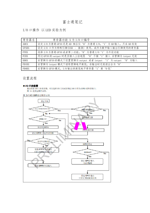
富士通笔记I/O口操作以LED实验为例设置流程以按键控制LED为例初始化LED管脚PFR相应位为‘0’设置管脚为GPIO模式,PDOR 设置相应位1输出为1,DDR设置为输出模式相应位为1,key管脚初始化设置PFR相应位为‘0’,DDR相应位设置为‘0’,通过读取PDIR 判断输入情况*** 外部中断操作以EXTI KEY 为例操作流程设置管脚映射;如FM3_GPIO->EPFR06 |= (2 << 2);/* 将INT01映射到INT01_1 */使能外部中断通道如NVIC_EnableIRQ(EXINT0_7_IRQn); /* 使能ch.0 to ch.7的中断*/DMAC (直接内存访问控制器)以DMA_Memory_To_Memory为例DMAC:操作步骤1 具体如下设置首先DMACA:——》寄存器设置是否使能传送使能——》DMAC触发方式——》数据缓冲长度——》设置DMACB寄存器设置——》传输模式——》传输数据宽度——》设置传送源地址递增或者不变——》目标地址递增或者递减——》完成后是否使能中断源——》DMACSAX DMA传送源地址——》DMACDAX DMA 目标地址——》DMACR使能全局DMA——》(以下是打开了传输完成中断设置)——清除NVIC_ClearPendingIRQ(DMAC0_IRQn);DMAC中断——》使能NVIC_EnableIRQ(DMAC0_IRQn);——》设置优先级NVIC_SetPriority(DMAC0_IRQn, 1); (中断函数)中断标志位清零FM3_DMAC->DMACB0 &= ~(7ul << 16);双时钟定时器以32为周期中断模式为例例程步骤写入0xFFFFFFFF到Timer1IntClr清除中断源——》设置Timer1Control寄存器设置是否使能设置时一般为否,工作模式,中断使能,分频数值,计数模式32位or16位,bit0位设置处单次模式外一般为‘0‘。
ADD9000说明书

Automotive Digital Diagnostic Tools 汽车数字诊断专用工具系列汽车数字诊断工具箱技术手册北京爱德盛业科技有限公司ADD3500无线汽车异响探测仪汽车数字诊断工具箱ADD9000Automotive Digital Diagnostics Tools Kits目录一、汽车传感器模拟测试仪 (3)二、汽车专用万用表ADD51 (20)三、汽车专用红外测温仪 (23)四、汽车短路/断路检测仪ADD330 (36)五、汽车数字钳表 (44)六、汽车电解液/冷却液/检测仪ADD501 (49)七、空调专用数字温度计 (51)八、数字式激光转速表使用说明书 0九、数显测试电笔 (2)十、万用测试线 (4)一、汽车传感器模拟测试仪一.安全指引..................................................................................................................................3 二.重要提示..................................................................................................................................3 三.目测检查:..............................................................................................................................4 四.技术指标..................................................................................................................................4 五.仪器操作.. (11)一.安全指引z 戴上安全防护眼镜、 穿上安全工作服、不要带手饰和留长头发。
96000 Series RF Reference Source 操作员手册说明书

May 2014 (Simplified Chinese) © 2014 Fluke Corporation. All rights reserved. Specifications are subject to change without notice. All product names are trademarks of their respective companies.96000 SeriesRF Reference Source操作员手册有限担保及责任范围Fluke 公司保证其每一个Fluke的产品在正常使用及维护情形下,其用料和做工都是毫无瑕疵的。
保证期限是一年并从产品寄运日起开始计算。
零件、产品修理及服务的保证期是 90 天。
本保证只提供给从Fluke 授权经销商处购买的原购买者或最终用户, 且不包括保险丝、电池以及因误用、改变、疏忽、或非正常情况下的使用或搬运而损坏(根据 Fluke 的意见而定)的产品。
Fluke 保证在 90 天之内,软件会根据其功能指标运行,同时软件已经正确地被记录在没有损坏的媒介上。
Fluke 不能保证其软件没有错误或者在运行时不会中断。
Fluke 仅授权经销商将本保证提供给购买新的、未曾使用过的产品的最终用户。
经销商无权以 Fluke 的名义来给予其它任何担保。
保修服务仅限于从 Fluke 授权销售处所购买的产品,或购买者已付出适当的Fluke国际价格。
在某一国家购买而需要在另一国家维修的产品,Fluke 保留向购买者征收维修/更换零件进口费用的权利。
Fluke 的保证是有限的,在保用期间退回 Fluke 授权服务中心的损坏产品,Fluke有权决定采用退款、免费维修或把产品更换的方式处理。
欲取得保证服务,请和您附近的Fluke服务中心联系,或把产品寄到最靠近您的Fluke服务中心(请说明故障所在,预付邮资和保险费用,并以 FOB 目的地方式寄送)。
富士通单片机中文手册
富士通电子设备用户手册F2MC-16LX Starter kit用户手册2注意事项・本资料有关内容如有变更恕不另行通知。
・本资料内所记载的设备运行情况及电路实例均是以半导体设备的标准规格及正确的使用方法为前提的,我们并不保证实际使用时所有机械的正常运作。
因此,在使用此设备时,顾客将完全承担相应的使用责任。
如有因使用此设备而造成的损害,本公司将不承担任何责任。
・本资料内所记载的设备运行情况以及电路图内所含有的技术资料并不代表可以任意使用本公司以及第三责任方的专利权以及著作权。
禁止通过本资料对第三责任方的知识产权以及相关的权利进行侵犯。
本公司对于此类相关行为以及所产生的后果将不负任何责任。
・本资料内若含有属于《外国汇率以及外国贸易法》范畴内的商品,或者含有相关范畴内的技术,则在出口本商品时必须得到相关法律的认可。
Copyright© 2005 FUJITSU LIMITED ALL right reserved © Fujitsu3目录前言 (6)1Starter-kit的安装方法 (7)1.1PC机上的软件安装 (13)1.1.1USB驱动的安装 (14)1.1.2综合开发环境SOFTUNE(限定版)的安装 (15)1.1.3ACCEMIC MDE demo version(trial版)的安装 (20)1.1.4评测板的设定以及与PC机的连接 (24)1.1.5SOFTUNE的设定与启动 (27)1.1.6ACCEMIC MDE的设定与启动 (30)1.1.7ACCEMIC MDE退出 (44)1.1.8SOFTUNE的退出 (44)1.1.9关闭Accemic的情况下启动单片机 (45)2编写使LED闪烁的程序 (46)2.1关于LED的介绍 (46)2.2LED为何会发光 (47)2.3利用单片机使LED发光的方法 (48)2.4LED发光程序的制作及运行 (51)2.4.1程序概要 (51)2.4.2程序的制作与运行 (52)2.5LED闪烁程序的制作与运行 (54)2.5.1程序概要 (54)2.5.2程序的制作与运行 (55)3用开关SW控制LED的亮灭 (57)3.1单片机如何检测SW的状态 (57)3.2通过SW控制LED程序的制作与运行 (58)3.2.1程序概要 (59)3.2.2程序的制作与运行 (59)4如何使用蜂鸣器 (61)4.1蜂鸣器内所用的材料 (61)4.1.1压电性的特点 (61)4.1.2压电材料的应用 (62)4.2单片机与压电蜂鸣器 (62)-- © Fujitsu44.2.1自励式与他励式 (63)4.2.2由单片机发出的脉冲波 (63)4.3如何使用PPG使蜂鸣器发出声音 (63)4.3.1L幅宽与H幅宽的设定 (64)4.3.2PPG count clock (64)4.4蜂鸣器程序的制作与运行 (65)4.4.1程序概要 (65)4.4.2程序的制作与运行 (67)4.4.3改变蜂鸣器的音色 (68)5利用中断来控制LED (69)5.1“中断”的概念 (69)5.2利用“中断”来检测SW的状态的方法 (70)5.3通过SW控制LED的程序(中断法) (71)5.3.1程序概要 (71)5.3.2程序的制作与执行 (72)6利用timer(定时器)来使LED闪烁 (75)6.1什么叫timer(定时器) (75)6.2通过Timer中断控制LED闪烁的程序 (76)6.2.1程序概要 (76)6.2.2程序的制作与运行 (78)7如何使用A/D(模/数)转换器 (81)7.1模拟信号与数字信号 (81)7.1.1A/D转换器的概要 (82)7.1.2滑动变阻器 (83)7.2制作一个表示电压数值的程序 (83)7.2.1程序概要 (83)7.2.2程序的制作与执行 (87)8如何使用温度传感器 (89)8.1关于温度传感器 (89)8.2温度传感器的使用方法 (90)8.3制作一个表示温度的程序 (91)8.3.1程序概要 (91)8.3.2程序的制作与执行 (94)A附录A(程序制作流程) (96)B附录B(寄存器的写入/读出方法) (104)C附录C(头文件包含路径的设定方法) (105)© Fujitsu5前言首先,非常感谢您购买本公司的Starter-kit产品。
FMU90资料中文说明书
配备1个或 2个超声波探 头可 对明 渠和 测量 堰中 的介 质 进行流量测量 仅用1个探 头即 可同 时测 量溢 流情 形下 介质 的物 位和 流 量 具有回水检测(2个探头)功能或淤泥检测功能的流量 测量 最多可配置3个 累加 器( 不可 清零)和 3个计数器(可 清零) 提供用 于控 制外部 单元 的计 数脉 冲输 出或 时间 脉冲 输 出
Endress + Hauser
7
模拟量输出 继电器输出
Pronsonic S FMU90
输出
数目 输出信号
报警信号
1路或2路,取决于变送器的具体型号
根据变送器的具体型号进行配置: 带HART的4...20mA1) 不带HART的0...20mA
4...20mA(可选) — -10%(3.6mA) — 110%(22mA) — 保持(末次电流值) — 用户自定义 0...20mA — 110%(21.6mA) — 保持(末次电流值) — 用户自定义
数目 类型 指定功能
开关功率 故障信息
1个,3个或6个,取决于仪表的具体型号 无电势继电器,,可转换
界值(界内、界外、趋势指示、物位边界) 计数脉冲1)(脉冲宽度可调) 时间脉冲1)(脉冲宽度可调) 报警/诊断(如回水1)、淤泥1)、回波损耗指示) 泵控制(多级泵控制/固定边界检测/泵速率控制) FMU 90-*3**********和FMU 90-*4**********附加泵控制 格栅控制(差值测量或相对值测量) 现场总线继电器
输出阻尼 负载 最大脉动电压 最大噪声电压
在0...1000s 间自由选择 最大为600Ω,其它影响可忽略不计 Uss=200mV,频率处于47...125Hz间(负载:500Ω) Ueff=2.2mV,频率处于500...10kHz间(负载:500Ω)
用于家电产品的富士通8位微控制器系列
Dual-O.P.-FLASH 上列:48K字节 下列:12K字节 装载
F2MC-8FX MB95120系列
用于系统待机时的低功耗操作 ɾ使用计时器/计数器 硬件实现1分计数!
LCD控制器 ɾ最大可以显示128像素 ɾ带闪烁功能 →利用硬件实现闪烁,减低软件负荷! 用途: ɾ显示设定温度 ɾ显示实际温度 ɾ显示设定模式及设定参数 ɾ显示计时器设定时间
F2MC-8FX 开发环境的硬件构成如 图 4 所示,表 2 是开发工具一览表。
在该系列里,备有带有通用评估
表 1 品种构成和功能概要
项目 分类 ROM(FLASH)容量 RAM容量 时钟系统 CPU功能 IO端口(最大) 时基计时器 监视计时器 8/16bit复合计时器
8/16bitPPG计时器
16bitPPG计时器
12路
8路
可选择8或10比特分辨率。可选择采样/变换时间
12路
8路
可检出上沿,下沿,双沿
40seg×4com -
32seg×4com 5V产品为选项。可监测电源电压,电压低下时由内部发生复位信号。
停止/休止/辅助时钟/时钟方式
LQFP-100(引脚间距0.5mm) QFP-100(引脚间距0.65mm)
̚
客户目标
表 2 开发环境一览表
后台监视器 调试专用适配器 MCU面板 (装有评估芯片)
封装转换用转换板 评估面板
软件
MB95120系列
MB95160M系列
MB2146-09(BGM适配器)
MB2146-301A (MB95FV100D-101:
装有3V 专用品)
MB2146-303A (MB95FV100D-103:
Fujitsu USB Port Replicator PR09 数据册说明书
Data SheetFujitsu Accessory USB Port Replicator PR09 ConnectivityHigh-End Smart ConnectivityThe Fujitsu USB Port Replicator PR09 is the perfect solution for shared desk environments within a hyperconnected world. It connects your mobile system to your main peripherals with a single USB plug. This Port Replicator is equipped with the most powerful DisplayLink chipset supporting high performance video streaming with Dualhead-DisplayPort. Highest data throughput is guaranteed due to an USB Type-C based Gen2 Hub-Controller enabling up to 10 Gbit/s data streaming. The newest version of USB Power Delivery chipset (PD3.0) provides powerful charging during your workday.Main FeaturesDualhead high-end graphics up to 4kSinglehead up to 5kGigabit-LAN integratedUSB Type-C upstreamUSB Power Delivery (PD3.0)Multiport USB 3.1 Gen1 DFP hubMultiport USB 3.1 Gen2 DFP hubSPDIF digital audio 2.0HighlightsDeveloped for shared multi-vendor system workplacesSystem independent investment protection (TCO)Future proof & backwards compatible (e.g. to USB-A systems)Easy IT integration (PXE / MAC spoofing support)Mac Address Pass Through (MAPT) for Fujitsu Notebooks enabling MAPT in the BIOS from S3 or lower.Fast one-cable connection for data and powerGlobal country certificationsAppealing design ID workplace deviceReliabilityHighest availabilityExperience out of huge installed base of Fujitsu USB Port ReplicatorsUSB Port Replicator PR09Technical specificationsLED On/Off switch (blue)USB Power Delivery (amber)USB connection (green)LAN traffic, rear side (green/yellow) Color BlackRefresh rateSupported refresh rate (32 bit color depth)1x up to 5,120 x 2,880 @ 60 Hz 2x up to 4,096 x 2,160 @ 60 HzInterfacesPower on switch 1 default: ON (PR09 from Rev.:02)Power supply 1 AC/DC Power Adapter 120 W (package content)DC-in20 VUSB downstream7 (4x USB-A & 3x USB-C)USB upstream via USB Type-C cable (1 m)USB Type-C (UFP) 1 w/ USB PD (60 W)USB Type-C 3.1 Gen2 (DFP) 3 thereof 1x BC1.2 w/ 10.5 WUSB Type-C cable 1 (5A Gen2) (package content)USB Type-A 3.1 Gen1 (DFP)4DisplayPort 2 (DP1.2a as Dualmode DP++)Audio 1 SPDIF (2.0)Ethernet (RJ-45) 1 x Gigabit LAN (based on chip Realtek RTL8211F)Notes For Notebook-systems still using USB Type-A:order USB-A to USB-C Adapter S26391-F6058-L102 (1pc.)Several adapters availble: /de/products/computing/peripheral/accessories/connectivity Kensington Lock support yesSystem requirementsRequired interface USB Type-CSystem requirements For office and productivity:Intel Core i3 2+ GHz / Intel Core M / AMD Trinity or betterUSB 3.1 Gen 2 recommanded40MB of free storage spaceSupported operating systems Windows 11Windows 10Windows 7Special featuresUSB power delivery ver 3.0DisplayLink“Plug and Display” certifiedUSB downstream7 (4x USB-A & 3x USB-C)USB upstream via USB Type-C cable (1 m)Electrical valuesPower consumption Maximum usage: 120 WAverage office usage: 82 WWithout USB PD: 3 WDC Off: 0.07 WPower supply input100-240 V AC50-60 HzPower supply output20 V DC at 6 AComplianceEurope CESwitzerland ENVRussia EACUSA/Canada FCC Class BICES-003 Class BcTUVusUL/cULJapan JEITAVCCIPSE (AC-Adapter)JISCSouth Korea KCSingapore S-MarkChina CCC (AC-Adapter)Australia/New Zealand RCMTaiwan BSMISaudi Arabia SASOCompliance link https:///sites/certificatesDimensions / Weight / EnvironmentalMiscellaneous MAC address showDimensions (W x D x H)200 x 97.6 x 29 mmCable length USB-C cable: 1 mWeight340 g (device only w/o AC-Adapter)Operating ambient temperature 5 - 35 °C (41 - 95 °F)Storage ambient temperature 5 - 45 °C (41 - 113 °F)Operating relative humidity10 - 85 % (non condensing)Package contentUSB Port Replicator PR09AC/DC Adapter 20 V, 120 WEU-power cord, 1,8 mUSB Type-C cable, 1 mQuick Start GuideService Desk & Warranty InformationsSafety NotesInformationcard for driver downloadOrder codeS26391-F6007-L500EAN: 4057185642316WarrantyWarranty period 3 yearsWarranty type Bring-In / Send-In Service (depending on country)Warranty Terms & Conditions /warrantyDigital bug fixes Subject to availability and following their generic release for the product, bug fixes and function-preserving patchesfor product-related software (firmware) can be downloaded from the technical support at: https://support.ts.fujitsu.com/ free of charge by entering the respective product serial number. For application software supplied togetherwith the product, please directly refer to the support websites of the respective software manufacturer.Spare Parts availability at least 5 years after shipment, for details see https:///Service Weblink /emeia/products/product-support-services/CONTACTFujitsu Technology Solutions GmbH Website: 2023-11-27 EM-ENworldwide project for reducing burdens on the environment.Using our global know-how, we aim to contribute to the creation of a sustainable environment for future generations through IT.Please find further information at http://www./global/about/environmenttechnical specification with the maximum selection of components for the named system and not the detailed scope ofdelivery. The scope of delivery is defined by the selection of components at the time of ordering.Technical data is subject to modification and delivery subject to availability. Any liability that the data and illustrations are complete, actual or correct is excluded. Designations may be trademarks and/or copyrights of the respective owner, the use of which by third parties for their own purposes may infringe the rights of such owner.The overall product has been designed and manufactured for general office use, regular personal use and ordinary industrial use.More informationAll rights reserved, including intellectual property rights. Designations may be trademarks and/or copyrights of therespective owner, the use of which by third parties for their own purposes may infringe the rights of such owner. For further information see https:///global/about/resources/terms/ Copyright 2023 Fujitsu Technology Solutions GmbH。
- 1、下载文档前请自行甄别文档内容的完整性,平台不提供额外的编辑、内容补充、找答案等附加服务。
- 2、"仅部分预览"的文档,不可在线预览部分如存在完整性等问题,可反馈申请退款(可完整预览的文档不适用该条件!)。
- 3、如文档侵犯您的权益,请联系客服反馈,我们会尽快为您处理(人工客服工作时间:9:00-18:30)。
■DESCRIPTIONSThe FUJITSU MB90920 Series is a 16-bit general purpose high-capacity microcontroller designed for vehicle meter control applications etc.The instruction set retains the same AT architecture as the FUJITSU original F2MC-8L and F2MC-16L series, with further refinements including high-level language instructions, expanded addressing mode, enhanced (signed) multipler-divider computation and bit processing.In addition, a 32-bit accumulator is built in to enable long word processing.■FEATURES•ClockBuilt-in PLL clock frequency multiplication circuit.Selection of machine clocks (PLL clocks) is allowed among frequency division by 2 on oscillation clock and multiplication of 1 to 4 times of oscillation clock(for 4MHz oscillation clock, 4Hz to 16MHz).Operation by sub-clock(up to 50KHz : 100KHz oscillation clock divided by 2).(Continued)■PACKAGESMB90920 Series2•16-bit input capture (4 channels)Detects rising, falling, or both edges.16-bit capture register × 4Pin input edge detection latches the 16-bit free-run timer counter value, and generates an interrupt request.•16-bit reload timer (2 channels)16-bit reload timer operation (select toggle output or one-shot output)Event count function selection provided•Real Time Watch timer (main clock)Operates directly from oscillator clock.Compensates for oscillator deviationRead/write enabled second/minute/hour/date registerSignal interrupt•16-bit PPG (3channels)Output pins (3) , external trigger input pin (1)Output clock frequencies : f CP, f CP/22, f CP/24, f CP/26•Delay interruptGenerates interrupt for task switching.Interruptions to CPU can be generated/deleted by software setting.•External interrupts (8 channels)8-channel independent operationInterrupt source setting available : “L” to “H” edge/ “H” to “L” edge/ “L” level/ “H” level.•A/D converter10-bit or 8-bit resolution × 8 channels (input multiplexed)Conversion time : 2.6µs (at f CP= 16 MHz)External trigger startup available (P50/INT0/ADTG)Internal timer startup available (16-bit reload timer 1)•UART(LIN/SCI) (2 channels)Equipped with full duplex double bufferClock-asynchronous or clock-synchronous serial transmission is available•SIO (1 channels)Clock synchronized data transmission.LSB-first or MSB-first data transmission selection are available.•CAN interfaceConforms to CAN specifications version 2.0 Part A and B.Automatic resend in case of error.Automatic transfer in response to remote frame.16 prioritized message buffers for data and messages for data and IDMultiple message supportReceiving filter has flexible configuration : All bit compare/all bit mask/two partial bit masksSupports up to 1 MbpsCAN WAKEUP function (connects RX internally to INT0)•LCD controller/driver (32 segment x 4 common)Segment driver and command driver with direct LCD panel (display) drive capability•Low voltage/Program Looping detect resetAutomatic reset when low voltage is detectedProgram Looping detection function(Continued)MB90920 Series3 (Continued)•Stepping motor controller (4 channels)High current output for all channels × 4Synchronized 8/10-bit PWM for all channels × 2•Sound generator8-bit PWM signal mixed with tone frequency from 8-bit reload counter.PWM frequencies : 62.5 kHz, 31.2 kHz, 15.6 kHz, 7.8kHz (at f CP= 16MHz)Tone frequencies : 1/2 PWM frequency, divided by (reload frequency +1)•Input/output portsGeneral-purpose input/output port (CMOS output)- 70 ports (dual clock system)- 72 ports (single clock system)•Capable of changing input voltage for portAutomotive/CMOS-Schmitt (initial level is Automotive in single-chip mode)•Flash memory security functionProtect the content of FLASH memory (FLASH memory device only)MB90920 Series4■PRODUCT LINEUP• MB90920 SeriesPart numberParameterMB90F927MB90F927S MB90V920MB90V920S Configuration Flash ROM model Flash ROM model Evaluation model Evaluation model CPU F2MC-16LX CPUSystem clockOn-chip PLL clock multiplier type ( × 1, × 2, × 3, × 4, 1/2 when PLL stopped)Minimum instruction execution time 62.5 ns (with 4 MHz oscillation clock PLL × 4) Sub-clock pin(X0A, X1A)Yes No Yes No ROM Flash ROM 64 KB ExternalRAM 4 KB10 KBI/O port70 (sub-clock pins exist) / 72 (sub-clock pins not exist)SIO 1 ChannelLCD segment32UART UART(LIN/SCI) 2 ChannelsCAN 1 Channel16-Bit Input Capture 4 Channels16-Bit Reload Timer 2 Channels16-Bit Free Run Timer 1 ChannelReal Time Watch Timer 1 Channel16-bit PPG 3 ChannelsExternal Interrupt8 ChannelsA/D converter8 ChannelsLVD/CPU Loop Reset Yes NoStepping Motro Control 4 ChannelsSound Generator 1 ChannelFlash Security Yes NoOperation Voltage 3.7V ~ 5.5V 4.5V ~ 5.5VPackages QFP100, LQFP100PGA-299MB90920 Series5■PIN ASSIGNMENTSMB90920 Series 6MB90920 Series7■PIN DESCRIPTIONSPin no.SymbolCircuittypeDescriptionLQFP QFP8082X0AHigh speed oscillator input pin.8183X1High speed oscillator output pin.7880P92G General purpose I/O port.X0A ALow speed oscillator input pin. If no oscillator is connected,apply pull-down processing.7779P93G General purpose I/O port.X1A ALow speed oscillator output pin. If no oscillator is connected,leave open.7577RST B Reset input pin.8385P00JGeneral purpose input/output port.SIN0UART ch.0 serial data input pin.INT4INT4 external interrupt input pin.SEG24LCD segment output.8486P01EGeneral purpose input/output port.SOT0UART ch.0 serial data output pin.INT5INT5 external interrupt input pin.SEG25LCD segment output.8587P02EGeneral purpose input/output port.SCK0UART ch.0 serial clock input/output pin.INT6INT6 external interrupt input pin.SEG26LCD segment output.8688P03JGeneral purpose input/output port.SIN1UART ch.1 serial data input pin.INT7INT7 external interrupt input pin.SEG27LCD segment output.8789P04EGeneral purpose input/output port.SOT1UART ch.1 serial data output pin.SEG28LCD segment output.8890P05EGeneral purpose input/output port.SCK1UART ch.1 serial clock input/output pin.TRG16-bit PPG ch.0-2 external trigger input pin.SEG29LCD segment output.MB90920 Series 8MB90920 Series9(Continued) Pin no.SymbolCircuittypeDescriptionLQFP QFP4547P51KGeneral purpose input output port.INT1INT1 external interrupt input pin.SI SIO data input pin.4648P52GGeneral purpose input output port.INT2INT2 external interrupt input pin.SO SIO data ouput pin.5052P53GGeneral purpose input output port.INT3INT3 external interrupt input pin.SCK SIO clock input pin.52 to 5554 to 57P70 to P73HGeneral purpose input output ports.PWM1P0PWM1M0PWM2P0PWM2M0Stepping motor controller ch.0 output pins.57 to 6059 to 62P74 to P77HGeneral purpose input output ports.PWM1P1PWM1M1PWM2P1PWM2M1Stepping motor controller ch.1 output pins.62 to 6564 to 67P80 to P83HGeneral purpose input output ports.PWM1P2PWM1M2PWM2P2PWM2M2Stepping motor controller ch.2 output pins.67 to 7069 to 72P84 to P87HGeneral purpose input output ports.PWM1P3PWM1M3PWM2P3PWM2M3Stepping motor controller ch.3 output pins.7274P54GGeneral purpose input output port.TX0CAN interface 0 TX output pin.7375P55GGeneral purpose output port.RX0CAN interface 0 RX input pin.7476P56GGeneral purpose input output port.SGO Sound generator SG0 output pin.FRCK Free-run timer clock input pin.MB90920 Series10Note:*1 : Type C in MB90F927 and MB90F927S, type D in MB90V920 and MB90V920S.Pin no.SymbolCircuittypeDescriptionLQFP QFP7678P57GGeneral purpose input output port.SGA Sound generator SGA output pin.28 to 3130 to 33V0 to V3 LCD controller /driver reference power supply pins.56, 6658, 68DV CCHigh current output buffer with dedicated power supply input pins(pin numbers 54-57, 59-62, 64-67, 69-72) .51, 61, 7153, 63, 73DV SSHigh current output buffer with dedicated power supply GND pins(pin numbers 54-57, 59-62, 64-67, 69-72) .3234AV CC A/D converter dedicated power supply input pin.3537AV SS A/D converter dedicated GND supply pin.3335AVRH A/D converter Vref + input pin.47484950MD0MD1C Test mode input pins. Connect to V CC.4951MD2C/D*1Test mode input pin. Connect to V SS.2527CExternal capacitor pin. Connect an 0.1 µF capacitor between thispin and V SS.21, 8223, 84V CC Power supply input pins.9, 40, 7911, 42, 81V SS GND power supply pins.■I/O CIRCUIT TYPE(Continued)(Continued)(Continued)■HANDLING DEVICESPrecautions for Handling Semiconductor Devices•Strictly observe maximum rated voltages (prevent latchup)When CMOS integrated circuit devices are subjected to applied voltages higher than V CC at input and output pins other than medium- and high-withstand voltage pins, or to voltages lower than V SS, or when voltages in excess of rated levels are applied between V CC and V SS, a phenomenon known as latchup can occur. In a latchup condition, supply current can increase dramatically and may destroy semiconductor elements. In using semi-conductor devices, always take sufficient care to avoid exceeding maximum ratings.Also care must be taken when power to analog systems is switched on or off, to ensure that the analog power supply (AV CC, AVRH) , analog input and dedicated power supply for the high current output buffer pins (DV CC) do not exceed the digital power supply (V CC) .Once the digital power supply (V CC) is switched on, the analog power (AV CC,AVRH) and dedicated power supply for the high current output buffer pins (DV CC) may be turned on in any sequence.•Stable supply voltageEven within the warranted operating range of V CC supply voltage, sudden fluctuations in supply voltage can cause abnormal operation. The recommended stability for ripple fluctuations (P-P values) at commercial fre-quencies (50 Hz to 60 Hz) should be within 10% of the standard V CC value, and voltage fluctuations that occur during switching of power supplies etc. should be limited to transient fluctuation rates of 0.1 V/ms or less.•Power-on proceduresIn order to prevent abnormal operation of the internal built-in step-down circuits, voltage rise time during power-on should be attained within 50 µs (0.2 V to 2.7 V) .•Treatment of unused pinsIf unused input pins are left open, they may cause abnormal operation or latchup which may lead to permanent damage to the semiconductor. Any such pins should be pulled up or pulled down through resistance of at least2 kΩ.Any unused input/output pins should be left open in output status, or if found set to input status, they should be treated in the same way as input pins.Any unused output pins should be left open.•Treatment of A/D converter power supply pinsEven if the A/D converter is not used, pins should be connected so that AV CC= V CC, and AV SS= AVRH = V SS.•Use of external clock signalsEven when an external clock is used, a stabilization period is required following a power-on reset or release from sub clock mode or stop mode. Also, when an external clock is used it should drive only the X0 pin and the•Power supply pinsDevices are designed to prevent problems such as latchup when multiple V CC and V SS supply pins are used, by providing internal connections between pins having the same potential. However, in order to reduce unwanted radiation, and to prevent abnormal operation of strobe signals due to rise in ground level, and to maintain total output current ratings, all such pins should always be connected externally to power supplies and ground.As shown in figure below, all V CC power supply pins must have the same potential. All V SS power supply pins should be handled in the same way. If there are multiple V CC or V SS systems, the device will not operate properlyIn addition, care must be given to connecting the V CC and V SS pins of this device to a current source with as little impedance as possible. It is recommended that a bypass capacitor of 1.0 µF be connected between V CC and V SS as close to the pins as possible.•Proper sequence of A/D converter power supply analog inputA/D converter power (AV CC, AVRH) and analog input (AN0-AN7) must be applied after the digital power supply (V CC) is switched on. When power is shut off, the A/D converter power supply and analog input must be cut off before the digital power supply is switched on (V CC) . In both power-on and shut-off, care should be taken that AVRH does not exceed AV CC. Even when pins which double as analog input pins are used as input ports, be sure that the input voltage does not exceed AV CC. (There is no problem if analog power supplies and digital power supplies are turned off and on at the same time.)•Handling the power supply for high-current output buffer pins (DV CC, DV SS)Always apply power to high-current output buffer pins (DV CC, DV SS) after the digital power supply (V CC) is turned on. Also when switching power off, always shut off the power supply to the high-current output buffer pins (DV CC, DV SS) before switching off the digital power supply (V CC) . (There will be no problem if high-current output buffer pins and digital power supplies are turned off and on at the same time.)Even when high-current output buffer pins are used as general purpose ports, the power for high current output buffer pins (DV CC, DV SS) should be applied to these pins.•Pull-up/pull-down resistanceThe MB90920 series does not support internal pull-up/pull-down resistance. If necessary, use external compo-nents.•Precautions for when not using a sub clock signal.If the X0A and X1A pins are not connected to an oscillator, apply pull-down treatment to the X0A pin and leave the X1A pin open.•Notes on during operation when external clock is stopped.The microcontroller attempt to be working with the self-oscillating circuit even when there is no external oscillator or external clock input is stopped. Performance of this operation, however, cannot be guaranteed.■BLOCK DIAGRAM■MEMORY MAPNote : To select models without the ROM mirror function, see the “ROM Mirror Function Selection Module.” The image of the ROM data in the FF bank appears at the top of the 00 bank, in order to enable efficient use of small C compiler models. The lower 16-bit address for the FF bank will be assigned to the same address, so that tables in ROM can be referenced without declaring a “far” indication with the pointer. For example when accessing the address 00C000H, the actual access is to address FFC000H in ROM. Here the FF bank ROM area exceeds 48 KB, so that it is not possible to see the entire area in the 00 bank image. Therefore because the ROM data from FF4000H to FFFFFF H will appear in the image from 004000H to 00FFFF H, it is recommended that the ROM data table be stored in the area from FF4000H to FFFFFF H.■I/O MAP•Other than CAN Interface (Continued)Address Register name Symbol Read/write Peripheral functionInitial value 00H Port 0 data register PDR0R/W Port 0X X X X X X X X 01H Port 1 data register PDR1R/W Port 1- - XXXXXX 02H Port 2 data register PDR2R/W Port 2X X X X X X - -03H Port 3 data register PDR3R/W Port 3X X X X X X X X 04H Port 4 data register PDR4R/W Port 4X X X X X X X X 05H Port 5 data register PDR5R/W Port 5X X X X X X X X 06H Port 6 data register PDR6R/W Port 6X X X X X X X X 07H Port 7 data register PDR7R/W Port 7X X X X X X X X 08H Port 8 data register PDR8R/W Port 8X X X X X X X X 09H Port 9 data registerPDR9R/WPort 9- - - -X X X X0A H to 0F H (Disabled) 10H Port 0 direction register DDR0R/W Port 00 0 0 0 0 0 0 011H Port 1 direction register DDR1R/W Port 1- - 0 0 0 0 0 012H Port 2 direction register DDR2R/W Port 20 0 0 0 0 0 - -∗113H Port 3 direction register DDR3R/W Port 30 0 0 0 0 0 0 0∗114H Port 4 direction register DDR4R/W Port 40 0 0 0 0 0 0 015H Port 5 direction register DDR5R/W Port 50 0 0 0 0 0 0 016H Port 6 direction register DDR6R/W Port 60 0 0 0 0 0 0 017H Port 7 direction register DDR7R/W Port 70 0 0 0 0 0 0 018H Port 8 direction register DDR8R/W Port 80 0 0 0 0 0 0 019H Port 9 direction register DDR9R/W Port 9- - - - 0 0 0 01A H Analog input enable ADERR/WPort 6, A/D1 1 1 1 1 1 1 11B H to 1F H (Disabled) 20H A/D control status register lower ADCS0R/W A/D converter0 0 0 - - - - 021H A/D control status register higher ADCS1R/W 0 0 0 0 0 0 0 -22H A/D data register lower ADCR0R 0 0 0 0 0 0 0 023H A/D data register higher ADCR1R - - - - - - 0 024H Compare clear register CPCLR R/W 16-bit free-run timer X X X X X X X X 25H R/W X X X X X X X X 26H Timer data registerTCDT R/W 0 0 0 0 0 0 0 027H R/W 0 0 0 0 0 0 0 028H Timer control status register lower TCCSL R/W 0 0 0 0 0 0 0 029HTimer control status register higher TCCSHR/W0 1 - 0 0 0 0 0(Continued)(Continued)2122(Continued) Address Register name Symbol Read/write Peripheral function Initial value 80H PWM control register 0PWC0R/WStepping motorcontroller00 0 0 0 0 - - 081H (Disabled)82H PWM control register 1PWC1R/WStepping motorcontroller10 0 0 0 0 - - 083H (Disabled)84H PWM control register 2PWC2R/WStepping motorcontroller20 0 0 0 0 - - 085H (Disabled)86H PWM control register 3PWC3R/WStepping motorcontroller30 0 0 0 0 - - 0 87H to 89H (Disabled)8A H A/D setting register 0ADSR0R/WA/D0 0 0 0 0 0 0 08B H A/D setting register 1ADSR1R/W0 0 0 0 0 0 0 0 8C H Port Input Level Select 0PIL0R/W Port Input Level Se-lect0 0 0 0 0 0 0 08D H Port Input Level Select 1PIL1R/W- - - 0 0 0 0 0 8E H to9D H*4(Disabled)9E H ROM correction control register PACSR R/WAddress matchdetection function- - - - - 0 - 0 9F H Delay interrupt/release DIRR R/W Delayed interrupt- - - - - - - 02324(Continued) C4H Serial mode register 1SMR1R/WUART(LIN/SCI) 10 0 0 0 0 0 0 0C5H Serial control register 1SCR1R/W0 0 0 0 0 0 0 0 C6HReception/Transmission data reg-ister 1RDR1/TDR1R/W0 0 0 0 0 0 0 0 C7H Serial status register 1SSR1R/W0 0 0 0 1 0 0 0 C8HExtended Communication ControlRegister 1ECCR1R/W0 0 0 0 0 0 X X C9H Extended Status Control Register 1ESCR1R/W0 0 0 0 0 1 0 0 CA H Baud Rate Generator Register 10BGR10R/W0 0 0 0 0 0 0 0 CB H Baud Rate Generator Register 11BGR11R/W0 0 0 0 0 0 0 0 CC H Watch timer control register lower WTCRL R/WReal-timewatch timer0 0 0 - - 0 0 0CD H Watch timer control register middle WTCRM R/W0 0 0 0 0 0 0 0 CE H Watch timer control register higher WTCRH R/W- - - - 0 0 0 0 CF H Subclock Control register SCCR W Subclock- - - - 0 0 0 0D0H toFF H(Disabled)1FF0H ROM correction address 0PADR0R/WAddress matchdetection functionX X X X X X X X 1FF1H ROM correction address 1PADR0R/W X X X X X X X X 1FF2H ROM correction address 2PADR0R/W X X X X X X X X 1FF3H ROM correction address 3PADR1R/W Address matchdetection functionX X X X X X X X 1FF4H ROM correction address 4PADR1R/W X X X X X X X X 1FF5H ROM correction address 5PADR1R/W X X X X X X X X Address Register name Symbol Read/write Peripheral function Initial value25(Continued)Address Register name Symbol Read/write Peripheral function Initial value3900H to 391F H (Disabled)3920H PPG0 down counter register PDCR0R 16-bit PPG 01 1 1 1 1 1 1 13921H 1 1 1 1 1 1 1 13922H PPG0 cycle setting register PCSR0W X X X X X X X X 3923H X X X X X X X X 3924H PPG0 duty setting registerPDUT0WX X X X X X X X 3925H X X X X X X X X3926H to 3927H (Disabled)3928H PPG1 down counter register PDCR1R 16-bit PPG 11 1 1 1 1 1 1 13929H 1 1 1 1 1 1 1 1392A H PPG1 cycle setting register PCSR1W X X X X X X X X 392B H X X X X X X X X 392C H PPG1 duty setting registerPDUT1WX X X X X X X X 392D H X X X X X X X X392E H to 392F H (Disabled)3930H PPG2 down counter register PDCR2R 16 bit PPG 21 1 1 1 1 1 1 13931H 1 1 1 1 1 1 1 13932H PPG2 cycle setting register PCSR2W X X X X X X X X 3933H X X X X X X X X 3934H PPG2 duty setting registerPDUT2WX X X X X X X X 3935H X X X X X X X X3936H to 3957H (Disabled)3958H Sub second data register WTBR R/W Real time watch timerX X X X X X X X3959H X X X X X X X X 395A H - - - X X X X X 395B H Second data register WTSR R/W - - 0 0 0 0 0 0395C H Minute data register WTMR R/W - - 0 0 0 0 0 0395D H Hour data register WTHR R/W - - - 0 0 0 0 0395E H Day data registerWTDRR/W0 0 - 0 0 0 0 1395F H(Disabled)3960H to396F H LCD display RAMVRAMR/WLCD controller/driver X X X X X X X X3970H(Disabled)26(Continued)Address Register name Symbol Read/write Peripheral function Initial value3971H to397F H (Disabled)3980HPWM1 compare register 0PWC10R/WStepping motorcontroller 0X X X X X X X X 3981H- - - - - -X X 3982HPWM2 compare register 0PWC20R/WX X X X X X X X 3983H- - - - - -X X 3984H PWM1 select register 0PWS10R/W- - 0 0 0 0 0 0 3985H PWM2 select register 0PWS20R/W- 0 0 0 0 0 0 0 3986H to3987H(Disabled)3988HPWM1 compare register 1PWC11R/WStepping motorcontroller 1X X X X X X X X 3989H- - - - - -X X 398A HPWM2 compare register 1PWC21R/WX X X X X X X X 398B H- - - - - -X X 398C H PWM1 select register 1PWS11R/W- - 0 0 0 0 0 0 398D H PWM2 select register 1PWS21R/W- 0 0 0 0 0 0 0 398E H to398F H(Disabled)3990HPWM1 compare register 2PWC12R/WStepping motorcontroller 2X X X X X X X X 3991H- - - - - -X X3992HPWM2 compare register 2PWC22R/WX X X X X X X X 3993H- - - - - -X X 3994H PWM1 select register 2PWS12R/W- - 0 0 0 0 0 0 3995H PWM2 select register 2PWS22R/W- 0 0 0 0 0 0 0 3996H to3997H(Disabled)3998HPWM1 compare register 3PWC13R/WStepping motorcontroller 3X X X X X X X X 3999H- - - - - -X X399A HPWM2 compare register 3PWC23R/WX X X X X X X X 399B H- - - - - -X X 399C H PWM1 select register 3PWS13R/W- - 0 0 0 0 0 0 399D H PWM2 select register 3PWS23R/W- 0 0 0 0 0 0 0 399E H to39FF H(Disabled)3A00H to3AFF HArea reserved for CAN interface 03B00H to3BFF H(Disabled)27•Initial value symbols : “0” initial value 0.“1” initial value 1.“X” initial value undetermined“-” initial value undetermined (none) •Write/read symbols : “R/W” read/write enabled “R” read only “W” write only•Addresses in the area 0000H to 00FF H are reserved for the principal functions of the MCU. Read access attempts to reserved areas will result in an “X” value. Also, write access to reserved areas is prohibited.Note:*1: P22/SEG0 to P27/SEG5 and P30/SEG6 to P35/SEG11 initially will be LCD segments output as LCD outputcontrol register LOCR1 (58H ) is “11111111B ” initially. To use Port 2 and Port 3 as the general-purpose input/output ports, please set LOCR1 to “00000000B ” to disable the LCD segment output first.3C00H to 3CFF H Area reserved for CAN interface 03D00H to 3DFF H (Disabled) 3E00H to 3EFF H(Disabled)Address Register nameSymbolRead/write Peripheral functionInitial value28•I/O Map for CAN Interface(Continued) Address Register name SymbolRead/writeInitial value000040HMessage buffer valid area BVALR (R/W) 0 0 0 0 0 0 0 00 0 0 0 0 0 0 0 000041H000042HTransmission request regHi ister TREQR (R/W) 0 0 0 0 0 0 0 00 0 0 0 0 0 0 0 000043H000044HTransmission cancel register TCANR (W) 0 0 0 0 0 0 0 00 0 0 0 0 0 0 0 000045H000046HTransmission completed register TCR (R/W) 0 0 0 0 0 0 0 00 0 0 0 0 0 0 0 000047H000048HReceiving completed register RCR (R/W) 0 0 0 0 0 0 0 00 0 0 0 0 0 0 0 000049H00004A HRemote request receiving register RRTRR (R/W) 0 0 0 0 0 0 0 00 0 0 0 0 0 0 0 00004B H00004C HReceiving overrun register ROVRR (R/W) 0 0 0 0 0 0 0 00 0 0 0 0 0 0 0 00004D H00004E HReceiving interrupt enable register RIER (R/W) 0 0 0 0 0 0 0 00 0 0 0 0 0 0 0 00004F H003C00HControl status register CSR(R/W, R) 0 0 - - - 0 0 00 - - - - 0 - 1 003C01H003C02HLast event indicator register LEIR (R/W) - - - - - - - -0 0 0 - 0 0 0 0 003C03H003C04HRX/TX error counter RTEC (R) 0 0 0 0 0 0 0 00 0 0 0 0 0 0 0 003C05H003C06HBit timing register BTR (R/W) - 1 1 1 1 1 1 1 1 1 1 1 1 1 1 1 003C07H003C08HIDE register IDER (R/W) XXXXXXXX XXXXXXXX 003C09H003C0A HTransmission RTR register TRTRR (R/W) 0 0 0 0 0 0 0 00 0 0 0 0 0 0 0 003C0B H003C0C HRemote frame receiving wait register RFWTR (R/W) XXXXXXXX XXXXXXXX 003C0D H003C0E HTransmission interrupt enable register TIER (R/W) 0 0 0 0 0 0 0 00 0 0 0 0 0 0 0 003C0F H29(Continued)Address Register name SymbolRead/writeInitial value003C10H Acceptance mask select register AMSR (R/W)XXXXXXXXXXXXXXXX 003C11H 003C12H XXXXXXXX XXXXXXXX 003C13H 003C14H Acceptance mask register 0AMR0 (R/W)XXXXXXXXXXXXXXXX 003C15H 003C16H XXXXX- - -XXXXXXXX 003C17H 003C18H Acceptance mask register 1AMR1 (R/W)XXXXXXXXXXXXXXXX 003C19H 003C1A H XXXXX- - -XXXXXXXX003C1B H003A00Hto 003A1F H General purpose RAM (R/W) XXXXXXXX to XXXXXXXX003A20H ID register 0IDR0(R/W)XXXXXXXXXXXXXXXX 003A21H 003A22H XXXXX- - -XXXXXXXX 003A23H 003A24H ID register 1IDR1(R/W)XXXXXXXXXXXXXXXX 003A25H 003A26H XXXXX- - -XXXXXXXX 003A27H 003A28H ID register 2IDR2(R/W)XXXXXXXXXXXXXXXX 003A29H 003A2A H XXXXX- - -XXXXXXXX 003A2B H 003A2C H ID register 3IDR3(R/W)XXXXXXXXXXXXXXXX 003A2D H 003A2E H XXXXX- - -XXXXXXXX 003A2F H 003A30H ID register 4IDR4(R/W)XXXXXXXXXXXXXXXX 003A31H 003A32H XXXXX- - -XXXXXXXX 003A33H30(Continued) Address Register name SymbolRead/writeInitial value003A34HID register 5IDR5 (R/W)XXXXXXXX XXXXXXXX 003A35H003A36HXXXXX- - -XXXXXXXX 003A37H003A38HID register 6IDR6 (R/W)XXXXXXXX XXXXXXXX 003A39H003A3A HXXXXX- - -XXXXXXXX 003A3B H003A3C HID register 7IDR7 (R/W)XXXXXXXX XXXXXXXX 003A3D H003A3E HXXXXX- - -XXXXXXXX 003A3F H003A40HID register 8IDR8 (R/W)XXXXXXXX XXXXXXXX 003A41H003A42HXXXXX- - -XXXXXXXX 003A43H003A44HID register 9IDR9 (R/W)XXXXXXXX XXXXXXXX 003A45H003A46HXXXXX- - -XXXXXXXX 003A47H003A48HID register 10IDR10 (R/W)XXXXXXXX XXXXXXXX 003A49H003A4A HXXXXX- - -XXXXXXXX 003A4B H003A4C HID register 11IDR11 (R/W)XXXXXXXX XXXXXXXX 003A4D H003A4E HXXXXX- - -XXXXXXXX 003A4F H003A50HID register 12IDR12 (R/W)XXXXXXXX XXXXXXXX 003A51H003A52HXXXXX- - -XXXXXXXX 003A53H31(Continued)Address Register name SymbolRead/writeInitial value003A54H ID register 13IDR13 (R/W)XXXXXXXXXXXXXXXX 003A55H 003A56H XXXXX- - -XXXXXXXX 003A57H 003A58H ID register 14IDR14 (R/W)XXXXXXXXXXXXXXXX 003A59H 003A5A H XXXXX- - -XXXXXXXX 003A5B H 003A5C H ID register 15IDR15 (R/W)XXXXXXXXXXXXXXXX 003A5D H 003A5E H XXXXX- - -XXXXXXXX 003A5F H 003A60H DLC register 0DLCR0 (R/W) - - - -XXXX - - - -XXXX 003A61H 003A62H DLC register 1DLCR1 (R/W) - - - -XXXX - - - -XXXX 003A63H 003A64H DLC register 2DLCR2 (R/W) - - - -XXXX - - - -XXXX 003A65H 003A66H DLC register 3DLCR3 (R/W) - - - -XXXX - - - -XXXX 003A67H 003A68H DLC register 4DLCR4 (R/W) - - - -XXXX - - - -XXXX 003A69H 003A6A H DLC register 5DLCR5 (R/W) - - - -XXXX - - - -XXXX 003A6B H 003A6C H DLC register 6DLCR6 (R/W) - - - -XXXX - - - -XXXX 003A6D H 003A6E H DLC register 7DLCR7 (R/W) - - - -XXXX - - - -XXXX 003A6F H 003A70H DLC register 8DLCR8 (R/W) - - - -XXXX - - - -XXXX 003A71H 003A72H DLC register 9DLCR9 (R/W) - - - -XXXX - - - -XXXX 003A73H 003A74H DLC register 10DLCR10(R/W)- - - -XXXX- - - -XXXX 003A75H。