A 5-GHz BiCMOS variable-gain low noise amplifier with inductorless low-gain branch
基于负反馈技术的嵌套式直流失调消除电路
微电子技术基于负反馈技术的嵌套式直流失调消除电路鄢张芳玲打雷倩倩打张旭东打李弦2,李连碧1(1.西安工程大学理学院,陕西西安710000;2.深圳市纽瑞芯科技有限公司,广东深圳518000)摘要:基于UMC40nm CMOS工艺,设计了一种带有直流失调消除电路(DCOC)的可编程增益放大器(PGA),该PGA采用闭环电阻反馈结构,由两级增益单元级联构成。
DCOC电路基于传统的直流负反馈结构,针对多级级联的方式,提出了一种嵌套式反馈方法,可降低电路功耗和面积。
仿真结果表明,DCOC在0-52dB的增益变化范围内高通截止频率恒为10kHz,相对抑制度恒为50dB,且在0dB时可矫正的最大输入失调量为110mV。
与传统设计方法相比,DCOC的面积减小近一半。
关键词:直流失调消除;嵌套式反馈;可编程增益放大器中图分类号:TN722文献标识码:A DOI:10.16157/j.issn.0258-7998.201136中文引用格式:张芳玲,雷倩倩,张旭东,等.基于负反馈技术的嵌套式直流失调消除电路[J].电子技术应用袁2021,47 (5):50-5358.英文弓I用格式:Zhang Fangling,Lei Qianqian,Zhang Xudong,et al.A nested DC offset cancellation circuit based on negative feedback technique[J].Application of Electronic Technique,2021,47(5):50-53,58.A nested DC offset cancellation circuit based on negative feedback techniqueZhang Fangling1,Lei Qianqian1,Zhang Xudong1,Li Xian2,LI Lianbi1(1.School of Science,Xi'an Polytechnic University,Xi'an710000,China;2.Shenzhen Niureixin Technology Co.,Ltd.,Shenzhen518000,China)Abstract:Based on the UMC40nm CMOS process,a programmable gain amplifier(PGA)with DC offset cancellation circuit(DCOC) is designed.The PGA adopts a closed-loop resistance negative feedback structure and consists of a cascade of two gain units. DCOC circuit is based on the traditional DC negative feedback structure,a nested feedback method is proposed to reduce the power consumption and area of DCOC circuit.The simulation results show that within the gain variation control range of0~52dB,the high pass cutoff frequency and the relative inhibition degree of DCOC are constant at10kHz and50dB,and the maximum correctable input misalignment at0dB pared with the traditional design method,the area of DCOC has been reduced by almost half.Key words:DC offset cancellation;nested feedback;programmable gain amplifier0引言随着可编程增益放大器(Programmable Gain Amplifier, PGA)放大倍数的增大,尤其在给接收链路提供较大增益时[1-3],直流失调的问题就越来越严重,使得下一级电路处于饱和状态。
(8)LNA 低噪声功放 Low Noise Amplifier Design 030724
|S- CFi| = rFi 為S-Plane上的圓方程式,並稱之為constant noise figure circle
圓心 min CFi 1 Ni
半徑
1 rFi Ni2 Ni (1 min )2 1 Ni
2 Fi Fmin where Ni 1 min 4rn
min=|min|qmin Minimum-noise source reflection coefficient @ F= Fmin
中華大學電機系 田慶誠
4
Noise Parameters of the Transistor
GaAs FET ATF-10136 Noise Parameters
Noise factor Noise figure
中華大學電機系 田慶誠
Si / Ni N F 1 So / No G
NF 10 log F (dB )
3
(Ni=kT0B=-174dBm/Hz+Bandwidth(dBHz) @ T=T0=290° K)
Noise Figure of a Two-Port Networks
Frequency dependent
Bias dependent
中華大學電機系 田慶誠
5
Noise Parameters from Linear Model
Touchstone-format S-parameters with noise data
! SIEMENS Discrete & RF Semiconductors ! BFP420 ! Si NPN RF SIEGET Grounded Emitter Transistor in SOT343 ! VCE = 1 V IC = 1.5 mA February 1998 S12 S22 MAG ANG MAG ANG ! Common Emitter S-Parameters: ! ! f ! GHz 0.450 0.900 Fmin Gammaopt rn/50 dB MAG ANG 0.71 0.32 21 0.35 0.76 0.51 34 0.27
Low Noise Amplifier for 3.5 GHz using the Agilent ATF-35143 Low Noise PHEMT
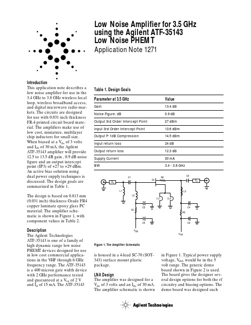
Low Noise Amplifier for 3.5 GHzusing the Agilent ATF-35143Low Noise PHEMTApplication Note 1271IntroductionThis application note describes alow noise amplifier for use in the3.4 GHz to 3.8 GHz wireless local loop, wireless broadband access, and digital microwave radio mar-kets. The circuits are designed for use with 0.031 inch thickness FR-4 printed circuit board mate-rial. The amplifiers make use of low cost, miniature, multilayer chip inductors for small size. When biased at a V ds of 3 volts and I ds of 30 mA, the Agilent ATF-35143 amplifier will provide 12.5 to 13.5 dB gain , 0.9 dB noise figure and an output intercept point (IP3) of +27 to +29 dBm. An active bias solution using dual power supply techniques is discussed. The design goals are summarized in Table 1.The design is based on 0.813 mm (0.031 inch) thickness Grade FR4 copper laminate epoxy glass PC material. The amplifier sche-matic is shown in Figure 1, with component values in Table 2. DescriptionThe Agilent TechnologiesATF-35143 is one of a family of high dynamic range low noise PHEMT devices designed for use in low cost commercial applica-tions in the VHF through 6 GHz frequency range. The ATF-35143 is a 400 micron gate width device with 2 GHz performance tested and guaranteed at a V ce of 2 V and I d of 15 mA. The ATF-35143Parameter at 3.5 GHz ValueGain13.4 dBNoise Figure, dB0.9 dBOutput 3rd Order Intercept Point27 dBmInput 3rd Order Intercept Point13.6 dBmOutput P-1dB Compression14.5 dBmInput return loss24 dBOutput return loss12.3 dBSupply Current30 mABW 3.4 - 3.8 GHzTable 1. Design Goalsis housed in a 4-lead SC-70 (SOT-343) surface mount plasticpackage.LNA DesignThe amplifier was designed for aV ds of 3 volts and an I ds of 30 mA.The amplifier schematic is shownin Figure 1. Typical power supplyvoltage, V dd, would be in the 5volt range. The generic demoboard shown in Figure 2 is used.The board gives the designer sev-eral design options for both the rfcircuitry and biasing options. Thedemo board was designed such Figure 1. The Amplifier Schematicddthat the input and output imped-ance matching networks can be either lumped element networks or etched microstrip networks for lower cost. Either low pass or high pass structures can be gener-ated based on system requirements. The demo board also allows the FET to be either self biased or with grounded sources the FET can be biased with a negative voltage applied to the gate terminal. The demo board is etched on 0.031" thick-ness FR-4 material for cost considerations.Biasing Options and Source GroundingPassive biasing schemes are gen-erally preferred for their simplicity. One method of passive biasing requires the source leads be direct dc grounded. A negative voltage is applied to the gate through a bias de-coupling net-work. The gate voltage is then adjusted for the desired value of drain current. The gate voltage required to support a desired drain current, I d, is dependent on the device’s pinchoff voltage, V p, and the saturated drain current, I dss. I d is calculated with the fol-lowing equation.Values for V gs may be calculated from the typical I-V curves found in the data sheet.The use of a controlled amount of source inductance can often be used to enhance LNA perfor-mance. Usually only a few tenths of a nanohenry or at most a few nanohenrys of inductance is re-quired. This is effectively equivalent to increasing the source leads by only 0.050 inch or so. The effect can be easily mod-eled using Agilent TechnologiesADS®. The usual side effect ofexcessive source inductance isvery high frequency gain peakingand resultant oscillations. Thelarger gate width devices haveless high frequency gain andtherefore the high frequency per-formance is not as sensitive tosource inductance as a smallerdevice would be. The ability of the400 micron gate width ATF-35143to tolerate greater source induc-tance allows the designer to takeadvantage of self biasing therebyonly necessitating a single posi-tive power supply.Design of ATF-35143 AmplifierThe parts list for the first ampli-fier is shown in Table 2. The demoboard as modified is shown in Fig-ure 3. The modifications arediscussed in the next section.The amplifier uses a high-pass im-pedance matching network forthe noise match. The high-passnetwork consists of a series ca-pacitor (C1) and a shunt inductorC1 1.5 pF chip capacitor (C1005COG1H1R5C)C2, C4 4.0 pF chip capacitor (C1005COG1H040C)C3 2.0 pF chip capacitor (C1005COG1H020C)C5, C61000 pF chip capacitorL1 2.2 nH inductor (Toko LL1005-FH2N2S)L2, L3 3.3 nH inductor (Toko LL1005-FH3N3)LL1, LL2Strap each source pad to the ground pad with 0.030"wide etch. The jumpered etch is placed a distance of0.037" away from the point where each source leadcontacts the source pad.Q1Agilent Technologies ATF-35143 PHEMTR147 Ω chip resistorR210 Ω chip resistor (Murata CR05-10RJ)R353 Ω chip resistorZo50 Ω MicrostriplineTable 2. Component Parts List for the ATF-35143 Amplifier.(L1). The demo board incorpo-rates series microstripline on theinput. It is not required for thisamplifier design and can be re-moved from the demo board. Itshould be replaced with a shuntinductor, L3. The circuit loss willdirectly relate to noise figure, thusQ of L3 is extremely important.The Toko LL1005-FH3N3 or simi-lar device is suitable for thispurpose. Shunt inductor (L1)provides low frequency gain re-duction, which can minimize theamplifier’s susceptibility to lowfrequency transmitter overload. Itis also part of the input matchingnetwork along with C1. C1 alsodoubles as a dc block. L2 alsodoubles as a means of insertinggate voltage for biasing up thePHEMT. This requires a good by-pass capacitor in the form of C2.The Q of L2 is also extremely im-portant from the standpoint ofcircuit loss, which will directlyrelate to noise figure. The TokoLL1005-FH2N2S is a small multi-layer chip inductor with a rated Qof 30 at 800 MHz. Lower elementQs may increase circuit noiseV gs = V p1–I d I dssfigure and should be considered carefully. This network has been a compromise between low noise figure, input return loss and gain.Resistor R2 and capacitors C2 and C4 provide in-band stability while resistors R1 and R3 provide low frequency stability by providing a resistive termination.Inductors LL1 and LL2 are actu-ally very short transmission lines between each source lead and ground. The inductors act as se-ries feedback. The amount of series feedback has a dramatic effect on in-band and out-of-band gain, stability and input and out-put return loss. The amplifier demo board is designed such that the amount of source inductance is variable. Each source lead is connected to a microstrip line,which can be connected to aground pad at any point along the line. For minimal inductance, the source lead pad is connected to the ground pad with a very short piece of etch at the point closest to the device source lead. For the amplifier, each source lead is con-nected to its corresponding ground pad at a distance of ap-proximately 0.037" from the source lead. The 0.037" is mea-sured from the edge of the source lead to the closest edge of the first via hole. The remaining un-used source lead pad should be removed by cutting off the unused etch. On occasion, the unused etch which looks like an open cir-cuited stub has caused highfrequency oscillations. During the initial prototype stage, the amount of source inductance can be tuned to optimize performance. More on this subject next.Determining the Optimum Amount of Source InductanceAdding additional source induc-tance has the positive effect of improving input return loss and low frequency stability. A poten-tial down side is reduced low frequency gain, however, de-creased gain also correlates to higher input intercept point. The question then becomes how much source inductance can one add before one has gone too far?For an amplifier operating in the 900 MHz frequency range, exces-sive source inductance will manifest itself in the form of a gain peak in the 6 to 10 GHz fre-quency range. Normally the high frequency gain roll-off will be gradual and smooth. Adding source inductance begins to add bumps to the once smooth roll-off. The source inductance, while having a degenerative effect at low frequencies, is having a regen-erative effect at higherfrequencies. This shows up as again peak in S21 and also shows up as input return loss S11 be-coming more positive. Some shift in upper frequency performance is acceptable as long as the amount of source inductance is fixed and has some margin in the design so as to account for S21variations in the device.Performance of the Agilent ATF-35143 AmplifierThe amplifier is biased at a V ds of 3 volts and I d of 30 mA. Typical V gs is -0.41 volts. The measured noise figure and gain of the com-pleted amplifier is shown inFigures 4 and 5. Noise figure is a nominal 1.0 dB from 3.0 through 4.0 GHz. Gain is a minimum of 11.5 dB at 4.0 GHz with a peak of 15.0 dB at 2.8 GHz.Measured input and output return loss is shown in Figure 6. The in-put return loss at 3.5 GHz is 24 dB with a corresponding output re-turn loss of 12.3 dB. Note that best input return loss and mini-mum noise figure do notnecessarily occur at the same fre-quency. This is due to Γo and S11*not occurring simultaneously at any one frequency. The amplifier output intercept point (OIP3) was measured at a nominal +27 dBm at a dc bias point of 3 volts V ds and an I d of 30 mA. P-1dB mea-sured +14.5 dBm.Figure 2. Artwork for the ATF-35143 Low Noise Amplifier.Figure 3. Component Placement Drawing forthe ATF-35143 Low Noise Amplifier0.710"Figure 6. Input and Output Return Loss vs. FrequencyFigure 4. Gain vs. FrequencyFigure 5. Noise Figure vs. FrequencyAgilent ATF-35143 Low Noise Amplifier DesignUsing Agilent Technologies Eesof Advanced Design System Soft-ware the amplifier circuit can be simulated in both linear and non-linear modes of operation. The original design draft was a low noise amplifier with an Output Third Order Intercept Point(OIP3) of 26-28 dBm with a noise figure close to 1.0 dB at 3.5 GHz.Linear AnalysisThe circuit used for the linear analysis is shown in Figure 7. The ATF35143.s2p file can be down-loaded from the Agilent Wireless Design Center web site. The 2-Port S-parameter file icon avail-able from the linear Data File Palette is used. A template for s-parameter evaluation is avail-able in ADS, the Sparams_wNoise template was chosen. The circuit components were added to the simulation circuit. The more de-tailed the simulation the more accurate the results will be. An accurate circuit simulation can provide the appropriate first step to a successful amplifier design.The inductance associated with the chip capacitors and resistors was included in the simulation.Where possible models were cho-sen from the ADS SMTcomponent library. Models of SMT components can also be ob-tained from the manufacturers ’web sites. Manufacturing toler-ances in both the active and passive components often pro-hibit perfect correlation. The results of the simulated noise fig-ure, gain, input and output return losses are shown in Figures 8, 9and 10. The linear simulated per-formance of the amplifier was very close to the measured re-sults.As noted on the data sheet, the ATF-35143 S and Noise Param-eters are tested in a fixture that includes plated through holes through a 0.025" thickness printed circuit board. Due to the complex-ity of de-embedding thesegrounds, the S and Noise Param-eters include the effects of the test fixture grounds. Therefore,when simulating a 0.031" thick-ness printed circuit board, only the difference in the printed cir-cuit board thickness is included in the simulation, i.e. 0.031" - 0.025"= 0.006". The transmission lines that connect each source lead to its corresponding plated through hole is simulated as a microstripline (MLIN).12345FREQUENCY (GHz)20151050G A I N (d B )2345FREQUENCY (GHz)21N O I S E F I G U R E (d B )FREQUENCY (GHz)R E T U R N L O S S (d B )Figure 7. ADS SchematicFigure 10. Linear Simulated Input and Output Return Loss vs. FrequencyFigure 8. Linear Simulated Gain vs. FrequencyFigure 9. Linear Simulated Noise Figure vs. FrequencyNon-Linear AnalysisThe circuit that is used for the non-linear analysis is identical to the linear analysis circuit. The 2-Port S-parameter file icon was replaced by the non-linear model for the ATF-35143. The model was downloaded from the Agilent Wireless Design Center. The ADS unarchive function was used to extract the model. See ADS for further details on unarchiving models.To perform the non-linear analy-sis the Harmonic Balancedcontroller or one of the other non-linear simulators, must be inserted into the schematic win-dow. The current probe and the node point were inserted to check that the bias conditions were cor-rect.The results of the simulated noise figure, gain, input and output re-turn losses are shown in Figures 11, 12 and 13. The Non-Linear simulator allows Agilent to simu-late the P-1dB and the Output Third Order Intercept Point. The amplifier OIP3 was simulated at +27.9 dBm and P-1dB +14.8 dBm.Non-linear simulated performanceof the amplifier was very close to the measured results. A summary of the Non-linear simulated per-formance is shown in Table 3.12345FREQUENCY (GHz)20151050G A I N (d B )2345FREQUENCY (GHz)210N O I S E F I G U R E (d B )FREQUENCY (GHz)R E T U R N L O S S (d B )Figure 13. Non-Linear Simulated Input and Output Return LossFigure 11. Non-Linear Simulated Noise Figure vs. FrequencyFigure 12. Non-Linear Simulated Gain vs. FrequencyBias Conditions Noise Figure P-1dB Third Order Intercept 2 V, 15 mA 0.7 dB 9.8 dBm 22.1 dBm 2 V, 30 mA 0.6 dB 12.9 dBm 27.5 dBm 3 V, 30 mA0.6 dB14.8 dBm27.9 dBmTable 3. Summary of Non-linear Simulated Performance 2345FREQUENCY (GHz)21N O I S E F I G U R E (d B )12345FREQUENCY (GHz)20151050G A I N (d B )FREQUENCY (GHz)R E T U R N L O S S (d B )/semiconductorsFor product information and a complete list of distributors, please go to our web site.For technical assistance call:Americas/Canada: +1 (800) 235-0312 or (408) 654-8675Europe: +49 (0) 6441 92460China: 10800 650 0017Hong Kong: (+65) 271 2451India, Australia, New Zealand: (+65) 271 2394Japan: (+81 3) 3335-8152(Domestic/International), or 0120-61-1280(Domestic Only)Korea: (+65) 271 2194Malaysia, Singapore: (+65) 271 2054Taiwan: (+65) 271 2654Data subject to change.Copyright © 2002 Agilent Technologies, Inc.January 3, 2002Circuit StabilityBesides providing important infor-mation regarding gain, noise figure, input and output return loss, the computer simulation pro-vides very important information regarding circuit stability. Unless a circuit is actually oscillating on the bench, it may be difficult to predict instabilities without actu-ally presenting various VSWR loads at various phase angles to the amplifier. Calculating the Rollett Stability factor K and gen-erating stability circles are two methods made considerablyeasier with computer simulations.The simulated gain, noise figure,and input/output return loss of the ATF-35143 amplifier are shown in Figures 8, 9 and 10. These plots only address the performance near the actual desired operating frequency. It is still important to analyze out-of-band performance in regards to abnormal gain peaks, positive return loss and stability. A plot of Rollett Stability factor K as calculated from0.1 GHz to 12 GHz is shown in Fig-ure 14 for the amplifier. Emitter inductance can be used to help stability. It should be noted how-ever that excessive inductance will cause high frequency stabilityFigure 14. Simulated Rollett Stability Factor Kto get worse (i.e., decreased value of K). The resistive loading, R2, is one of the main contributors to stability along with the induc-tance in the ground path.Increasing the value of R2 will make the stability factor K higher.As stability is improved, certain amplifier parameters such as gain and power output may have to be sacrificed.ConclusionThe amplifier design has been pre-sented using the AgilentTechnologies ATF-35143 low noise PHEMT. The ATF-35143provides a very low noise figure along with high intercept point making it ideal for applications where high dynamic range is re-quired. In addition to providing low noise figure, the ATF-35143can be simultaneously matched for very good input and output return loss, making it easilycascadable with other amplifiers and filters with minimal effect on system passband gain ripple.ReferencesPerformance data for the Agilent ATF-35143 PHEMT may be found on /view/rf Application NotesApplication Note 1197, “A Low Current, High Intercept Point,Low Noise Amplifier for 1900 MHz using the Agilent ATF-38143 Low Noise PHEMT ”Application Note 1174, “Low Noise Amplifiers for 1600 MHz and 1900 MHz Low Current Self-biased Applications using the ATF-35143 Low Noise PHEMT ”24681012FREQUENCY (GHz)109876543210R O L L E T T S T A B I L I T Y F A C T O R K。
信号经过LNA后信噪比会降低么

下图是Noise Figure跟Noise Factor的定义由上图可知 Noise Factor是大于等于1也就是说输出端的SNR 在最理想情况下顶多是跟输入端一样再怎样都不会比输入端大这也合理啦所谓Noise Figure,衡量的是当一个讯号进入一个系统时,其输出讯号的SNR下降多寡,亦即其噪声对系统的危害程度所以即便是Noise-less的系统 SNR不下降就谢天谢地了不太可能SNR还有所提升因此当增益压缩不存在时亦即输入讯号在LNA的线性范围内时原则上其讯号跟噪声的放大倍数一样也就是SNR是不变的最终输出SNR之所以会变小是来自于LNA自身的Additive Noise使得Noise Floor上升 SNR下降如下图所以为什么Tx要用PA ? 因为Tx端对功率要求高其放大器的放大倍数要大才有足够能量将讯号传送至天线并使之辐射出去为什么Rx要用LNA ? 因为Rx端对SNR要求高当然是希望其放大器的Additive Noise越小越好所以才叫Low Noise Amplifier 若Tx端用LNA 那放大倍数不够便无足够能量将讯号传送至天线反之若Rx用PA 其Additive Noise会非常非常大最终输出端SNR 铁定比输入端小很多而且也会因放大倍数太大使后端Mixer饱和那么整个接收端的灵敏度跟线性度都会变差那如果存在增益压缩呢? 那就是SNR会降更多当输入讯号过大时,会使LNA饱和,导致Gain下降,当然 Gain下降顶多是讯号跟噪声的放大倍数同时下降理论上SNR不变然而若LNA饱和其Noise Floor会上升更多亦即Additive Noise会比没饱和时更大所以其输出端SNR 会比没饱和时更小亦即SNR会降更多若LNA的Gain降为零,即输入讯号经过LNA时,完全不会被放大,则有可能完全被Noise Floor淹没,此时SNR便降为0而由以上可知即便讯号经过放大器其SNR都会降低更不要说无放大作用的组件不管是有源还是无源那怕是滤波器也一样因为滤波器只能砍带外噪声不能砍带内噪声而接收机整体的Noise Figure,公式如下:因此我们得出一个结论讯号经过任何组件其SNR就是会下降经过的电路越多,SNR下降越多,所以电路结构越简单越好但是如楼主所问若接收机的输出端的信噪比比输入端的信噪比还要低,这样是否有点失去了当初做接收机的意义?这分两部份探讨一个是LNA的存在意义下图是零中频接收机的架构图因为零中频架构,会直接将接收的射频讯号,透过ADC (Analog Digital Converter) 转换成数字讯号。
基于SiGe BiCMOS工艺的5GHz低噪声放大器的设计

显 著增 大 , 此时 若 继 续 增 大 电 流将 会 导 致 噪 声 上 升 J . 因此 , 设计 L N A 时 必 须折 中考 虑 噪声 和 功
耗, 本文 选 取 G r a c e公 司 0 . 1 8 I z m S i Ge B i C MOS
采用电感作为发射极 的串联反馈元件 , 集电极 负 载也采 用 电感元 件 . 图 4为射极 电感负反馈电路结构 , 其中c 为
_r b +
5 0 Q
( 3 )
输 入阻抗 的虚数部 分应 该为 零 , 即:
图 1 无线接收机系统示 意
L B+ ( 1 +卢) L E一— 一
对于 L NA 电路来 说 , 噪声 是其 最重 要 的性 能
指 标之 一 . 晶体 管 噪声 系 数 与 集 电 极 电流 和
通讯作者简介 : 阮颖 ( 1 9 7 8一) , 女, 博 士, 讲师 , 湖南株 洲人. 主要研究 方 向为射 频集成 电路 和器件 . E - ma i l : r u a n
—
y i n g@ 1 6 3. c o m.
基金项 目: 上海市科 技 创新 行动 计 划地 方 院校 能力 建 设项 目( 1 0 1 1 0 5 0 2 2 0 0 ) ; 教育 部 科 学技 术研 究 重点 项 目
( 2 1 0 0 7 2 ) .
阮
颖, 等: 基于 S i G e B i C MO S工艺 的 5 G Hz 低噪声放大器 的设计
双极 工 艺 和 标 准 的 互 补 金 属 氧 化 物 半 导 体
(C o mp l e me n t a r y Me t a l Ox i d e S e m i c o n d u c t o r ,
低噪声放大器工作原理
低噪声放大器工作原理介绍低噪声放大器(Low-Noise Amplifier,简称LNA)是一种常见的电子器件,其主要功能是将弱信号放大到足够的水平,以便能够有效地进行后续信号处理。
在无线通信、雷达系统等领域中,低噪声放大器起着至关重要的作用,它能够在信号传输过程中尽可能地减小噪声的加入,从而提高系统的信噪比。
工作原理低噪声放大器的工作原理涉及到放大器的各个组件和信号传输路径。
下面将详细介绍几个关键原理。
1. 放大器的输入部分低噪声放大器的输入部分通常包括天线、匹配网络和LNA芯片。
天线将接收到的微弱信号送入匹配网络,匹配网络对输入信号进行适当的调整,以保证信号能够最大程度地被传输到LNA芯片。
匹配网络的设计需要考虑到天线的阻抗、传输线等因素,以实现最佳的信号匹配。
2. 低噪声放大器的放大部分LNA芯片是低噪声放大器的核心组成部分,它负责将输入的微弱信号放大到合适的水平,同时尽可能地减小噪声。
为了实现低噪声放大,常见的设计方法包括:•使用低噪声场效应管(Low-Noise Field-Effect Transistor,简称LNA-FET)作为放大器的核心器件。
LNA-FET具有低噪声系数和高放大增益的特点,适合用于接收微弱信号。
•通过负反馈实现噪声抑制。
放大器的输出信号通过反馈回路与输入信号相比较,通过调节反馈网络的参数,可以抑制噪声的传输,从而提高信噪比。
•优化器件的工作状态和工作电压。
选择合适的工作状态和电压可以降低器件本身产生的噪声,并提高整个放大器系统的性能。
3. 噪声源和噪声参数低噪声放大器的性能评价与噪声参数密切相关。
主要的噪声源包括器件本身的噪声、传输线的噪声、温度噪声等。
常见的噪声参数有:•噪声系数(Noise Figure,简称NF):衡量放大器引入的噪声相对于理想放大器引入的噪声的影响程度。
噪声系数越低,表示放大器的噪声性能越好。
•噪声温度(Noise Temperature):用来表示放大器产生的等效噪声温度。
低噪声放大器..
5) C
C 0 VBC 1 0
n
反偏集电结电容
6) 7)
Ccs 集电结与衬底间的势垒电容
rbb ' 、ree 、 rcc 为各极的体电阻
大倍数下降为 1 时的频率
8) 特征频率 fT 定义为共射输出短路电流放
gm gm fT 2 (C C ) 2 C
3) 有源偏置电路
有源偏置电路具有相 当出色的温度稳定性,但 同时也带来了元件数目增 多,电路结构复杂等缺点。 在放大器的温度稳定性要 求比较高的时候,可以考 虑采用这种偏置电路。
有源偏置电路
3)传输线偏置电路
传输线偏置电路
传输线偏置法可以抑制偶次谐波,并且还可以 改善放大器的稳定性。
固定基流偏置电路
IIP3
Input VSWR
-11.1dBm
1.5
-3dBm
1.2
Output VSWR
隔 离
3.1
21dB
1.4
21dB
从表中可以看出,低噪声放大器的主要指标为: 噪声系数 增益 线性范围
输入输出阻抗的匹配
功耗
输入输出的隔离
以上各项指标并不独立,是相互关联的,在 设计中如何折中,兼须各项在指标,是设计的 重点也是难点。
C gd ---漏极与源极电容
rG 、 rS 、 rD 分别为各极的欧姆电阻,rds 是漏源电
阻, R 是串联栅极电阻 i
对于GaAs FET ,这些参数的典型值为
Ri 7
C gs 0.3 pF
rds 400 Cds 0.12 pF
gm 40mS
C gd 0.01 pF
基极分压射极偏置电路
2.4_GHz频段射频前端高线性度SiGe低噪声放大器设计
第50 卷第 10 期2023年10 月Vol.50,No.10Oct. 2023湖南大学学报(自然科学版)Journal of Hunan University(Natural Sciences)2.4 GHz频段射频前端高线性度SiGe低噪声放大器设计傅海鹏†,史昕宇(天津大学微电子学院,天津 300072)摘要:为满足高性能射频前端接收部分对高线性度的需求,基于SiGe BiCMOS工艺设计并实现了一款工作在2.4 GHz频段的高线性度低噪声放大器(Low Noise Amplifier,LNA).该放大器采用Cascode结构在增益与噪声之间取得平衡,在Cascode结构输入和输出间并联反馈电容,实现输入端噪声与增益的同时匹配.设计了一种改进的动态偏置有源电流镜以提升输入1 dB压缩点及输入三阶交调点的线性度指标.为满足应用需求,LNA与射频开关及电源模块集成组成低噪声射频前端接收芯片进行流片加工测试.测试结果表明:在工作频率2.4 ~2.5GHz内,整个接收芯片增益为14.6 ~15.2 dB,S11、S22<-9.8 dB,NF<2.1 dB,2.45 GHz输入1 dB压缩点为-2.7 dBm,输入三阶交调点为+12 dBm.芯片面积为1.23 mm×0.91 mm.该测试结果与仿真结果表现出较好的一致性,所设计的LNA展现出了较好的线性度表现.关键词:低噪声放大器;线性度;射频前端芯片;BiCMOS工艺中图分类号:TN402 文献标志码:ADesign of 2.4 GHz RF Front-end High Linearity SiGe Low Noise AmplifierFU Haipeng†,SHI Xinyu(School of Microelectronics,Tianjin University,Tianjin 300072,China)Abstract:To meet the high linearity requirement of high-performance RF front-end receivers, a high linearity low noise amplifier (LNA)operating at 2.4 GHz based on SiGe BiCMOS technology is proposed. The amplifier adopts the cascade structure to achieve a balance between gain and noise, and the feedback capacitor is connected in parallel between the input and output of the Cascode structure to achieve simultaneous noise and power match. An improved dynamic bias active current mirror is designed to improve the linearity parameters of the input 1 dB compression point and the input-referred third-order intercept point. To meet the requirements in application, LNA is integrated with an RF switch and power module to form an RF receiver front-end chip for processing and testing. The test results show that: within the operating frequency range of 2.4 ~ 2.5 GHz, the gain of the whole receiver chip is 14.6 ~ 15.2 dB. Return loss < -9.8 dB, and NF < 2.1 dB. At 2.45 GHz, the input 1 dB compression point is -2.7 dBm, and the input-referred third-order intercept point is +12 dBm. The chip area is 1.23 mm×0.91 mm. The test results are consistent with the simulation results, and the designed LNA exhibits good linearity performance.∗收稿日期:2023-02-22基金项目:国家自然科学基金资助项目(62074110),National Natural Science Foundation of China(62074110)作者简介:傅海鹏(1985—),男,黑龙江齐齐哈尔人,天津大学副教授† 通信联系人,E-mail:************.cn文章编号:1674-2974(2023)10-0077-07DOI:10.16339/ki.hdxbzkb.2023240湖南大学学报(自然科学版)2023 年Key words:low noise amplifiers;linearity;radio frequency front-end chip;BiCMOS technology低噪声放大器要求在自身不引入较大噪声的同时,将接收到的微弱信号进行线性放大.作为接收机中的第一个放大器,LNA的性能在很大程度上影响整个系统的噪声、线性度、灵敏度等指标.近年来,通信技术的发展和进步让视频会议、网络教学等各种应用场景得以实现,改变了人们的生活方式[1-3].为了适应不断扩大的接入设备数量,满足不断增长的数据吞吐量及速率需求,无线通信协议标准也在不断发展.其中,无线通信协议中诸如调制阶数的提升及系统灵敏度要求的提高对射频前端接收部分的线性度提出了更高的需求.这为LNA的设计带来了新的挑战,LNA需要具有更高的线性度、更低噪声、更高增益,以及更低的面积成本等[4].为实现高线性度需求,文献[5]采用多栅晶体管(Multiple Gated Transistor,MGTR)结构,分别将主、从CMOS晶体管偏置在饱和区和亚阈值区,实现对整体跨导二次导数的抵消,从而提升线性度.然而,该方案仅适用于CMOS工艺.文献[6]采用堆叠晶体管的方法设计了一种堆叠三级的cascode低噪声放大器.堆叠使得放大器可以使用更高的电源电压,从而获得更大的信号摆幅范围.功耗的提升也使得线性度得以提升.但这显著牺牲了功耗,不符合低功耗应用的发展趋势.文献[7]通过改进偏置电路提升线性度,但是其在大信号时,经电阻泄漏的射频电流会直接流入偏置电路中,偏置电路与放大器间镇流电阻的压降变化仍会带来低噪声放大器输入1 dB压缩点的前移,恶化放大器线性度.从工艺考虑,虽然CMOS工艺具有成本较低、易于集成等优势,但是噪声和线性度较差[8].而GaAs等Ⅲ/Ⅴ族工艺与之相反,性能优秀,但价格高昂且不易集成[9].与上述主流工艺对比,SiGe BiCMOS工艺不仅具有CMOS工艺易于集成的特点,还具有可与GaAs等Ⅲ/Ⅴ族工艺相比拟的性能和价格优势,是一种适合射频LNA设计的具有高性价比的折中选择[10].针对上述挑战并考虑工艺特点,本文采用SiGe BiCMOS工艺,设计并实现了一款工作在2.4 GHz频段的射频前端LNA.通过并联电容反馈技术在输入端同时实现增益和噪声匹配,并结合SiGe工艺特点,采用改进的动态偏置电路,克服镇流电阻压降影响,对泄漏的射频电流也加以利用,在不提升静态功耗的同时,实现线性度提升.为适应不同强度信号下的工作情况,该LNA可在LNA模式和旁路(Bypass)模式间切换.1 电路设计本文提出的全集成LNA整体框图如图1所示.整体电路由LNA、偏置电路、单刀双掷(Single PoleDouble Throw,SPDT)收发开关及Bypass支路构成.芯片整体通过单刀双掷开关选通发射、接收支路. LNA接收部分在输入信号较小时,通过逻辑控制开关使电路工作在LNA模式,实现低噪声放大功能.在输入信号较大时,电路工作在Bypass模式,对信号进行旁路衰减,供后级电路处理.1.1 开关设计本文使用的单刀双掷开关如图2所示.开关电路结构采用串并联结构,导通时开启串联支路,关闭并联支路,实现导通低插入损耗;关断时关闭串联支路,导通并联支路,实现关断高隔离度.由于发射、接收支路具有不同的功率容量需求,整体电路设计为非对称结构.当LNA_EN为高电平,PA_EN为低电平时,射频开关选通接收支路,M1管关断隔离发射支路,天线ANT端口接收信号经过M2、M3管从RX端输出至LNA主体放大;当LNA_EN为低电平,PA_EN为高电平时,M2、M3关断隔离接收支路,PA发出的大功率信号由TX端口经过M1管从ANT端输出.1.2 LNA及Bypass设计低噪声放大器在稳定的条件下,主要性能指标图1 全集成LNA框图Fig.1 Block diagram of fully integrated LNA78第 10 期傅海鹏等:2.4 GHz 频段射频前端高线性度SiGe 低噪声放大器设计包含噪声系数、增益及线性度,良好的设计需要在三者之间权衡折中,一般噪声系数和增益的优先级较高[11-12].本文所设计的LNA 放大器部分如图3所示,放大器主体由三极管Q CE 和Q CB 构成器件数较少的共射共基结构,减少晶体管噪声贡献并提高放大器增益.采用高Q 值的金丝键合线电感L S 组成发射极电感反馈结构保持放大器良好的稳定性,并参与输入阻抗实部匹配.考虑三极管在电流密度一定的条件下,其最小噪声系数将独立于晶体管大小.并且,共射共基极放大器的线性度与集电极工作电流I C 正相关.因此,在功耗范围内采用大尺寸、低电流密度的三极管实现噪声与线性度的折中设计.尽管这将导致输入阻抗的实部低于50 Ω,使输入匹配复杂化,但采用额外的并联电容反馈C F 和L 1、C 1构成的L 型匹配网络仍可以实现输入端噪声与增益的同时匹配.具体如图4所示,Z S 为50 Ω射频端口阻抗经过射频开关接收支路后在RX 端口体现的阻抗值.将L 1、C 1构成的L 型匹配网络输入阻抗设计为射频开关输出阻抗Z S 的共轭以实现最佳输入匹配,输出阻抗设计为共射共基放大器的最优信号源阻抗实现噪声匹配.并联反馈电容C F 将由负载电感L D 与电容C 3、C 4、C 5构成的T 型匹配网络共同组成的输出负载阻抗Z L 引入输入端匹配,因此可以通过调整C F 、Z L 来使看向晶体管的输入阻抗Z T 等于最佳噪源阻抗的共轭来实现增益匹配.由于引入的Z L 不在输入端,不会对先前噪声匹配产生明显影响,至此,也就实现了晶体管输入阻抗不为50 Ω时的输入端噪声与增益的同时匹配.且反馈电容C F 的引入使得反馈增强,稳定性提高,可以减小对L S 尺寸的需求,进一步优化噪声.结合图3、图4,可以推导出具体的输入阻抗为:Z IN =1sC 1//(sL 1+Z T )(1)Z T =Z 1s ()Z L +1sC FZ L ωT +s ()Z L +1sC F(2)Z 1=r BB +L S g m C BE +sL S +1sC BE(3)ωT =g m C BE(4)其中,C 1、L 1分别为L 型输入匹配的电容、电感,Z L 为负载电感L D 与电容C 3、C 4、C 5构成的T 型匹配网络共同组成的输出负载阻抗,C F 为并联反馈电容,r BB 为三极管小信号模型中的基极电阻,L S 为发射极反馈电感,g m 为三极管跨导,C BE 为三极管基极与发射极间寄生电容.当接收机接近信号源时,会接收到较大功率的信号,此时需要Bypass 功能对大功率信号进行旁路,避免信号超出接收电路动态范围,保护低噪声放大器不被损坏.当工作在Bypass 模式时,开关S 1、S 2、S 3、图2 单刀双掷开关原理图Fig.2 Schematic of single pole double throw switch图3 低噪声放大器原理图Fig.3 Schematic of the proposed dual-mode low noise amplifier图4 输入匹配原理图Fig.4 Schematic of the input matching network79湖南大学学报(自然科学版)2023 年S4断开,切断LNA通路.开关S5、S6打开,借由S5、S6开关的导通电阻与电阻R2和电容C7所在的支路一同构成T型衰减结构,并可以通过电容C6、C8分别调节Bypass模式下的输入、输出匹配特性,通过电容C7调整带内衰减平坦度,实现Bypass模式的信号衰减功能.1.3 线性度提升偏置电路设计偏置电路为晶体管提供合适的静态工作点.传统的有源偏置电路常采用电流镜结构,如图5所示.晶体管集电极电流I C与基极-发射极之间电压V BE的关系可写为:I C=I S exp(V BE V T)(5)式中:V T为热电压;I S为饱和电流.上式得出,当图5中晶体管Q2与Q3具有相同V BE 时,电流镜左右两边必然流过相同的电流.这就是电流镜的工作原理.假设LNA共射管Q CE叠加射频信号后,式(5)可改写为如式(6)所示,其中V RF为输入射频信号幅度.经过泰勒展开后可得式(7).I C=I S expéëêêV BE+V RF·sin ()2πft V Tùûúú(6)I C≈I S exp (V BE V T)éëêê54+sin (2πft)-cos ()4πft4ùûúúV RF V T(7)由上式可以得出,射频信号的输入会给集电极电流I C引入额外的直流分量,且随着输入射频信号增大,I C的直流部分将迅速升高.这意味着,随着输入射频信号增大,升高的I C将使得基极电流几乎同步升高,在镇流电阻上产生更大的压降,迫使共射管Q CE直流偏置电压降低,晶体管跨导下降,进而带来放大器增益的下降,使得放大器的1 dB压缩点提前到来,影响LNA线性度表现.因此,为提高LNA的线性度,本文采用如图6所示的动态偏置电路对LNA进行偏置.I Bias采用基准模块产生的恒定电流.将原本的镇流电阻R拆分为电阻R2、R3,则Q CE基极电流增大在R3上产生的额外压降仅会使得Q2各极电位同步抬升,避免了上述传统结构中镇流电阻对LNA线性度的影响.当LNA工作在小信号情况时,该偏置电路为放大器晶体管提供稳定偏置.而当输入射频信号增大,使得LNA共射管Q CE基极电压出现下降时,Q1基极电压将随之降低.同时,泄露的射频电流经C1流入R1,抬升Q1发射极电压,使得Q1集电极电流减小.此时,I Bias中将有更多电流成为Q2的基极电流,并经过Q2的电流放大作用,产生更多电流流入Q CE基极.最终,额外电流的注入将提高Q CE偏置电压,延缓Q CE跨导下降导致的放大器增益下降,实现动态偏置效果,提高LNA线性度.仿真得到在使用上述两种偏置电路时,Q CE晶体管基极-发射极电压V BE随输入功率变化的关系如图7所示.从图7可对比得出,使用传统电流镜偏置的晶体管V BE在输入功率高于-10 dBm后出现快速下降,并在输入功率达到+5 dBm时,已下降约200 mV.而同等条件下,采用动态偏置电路结构进行偏置的晶体管V BE仅下降10 mV.以上结果表明,动态偏置电图5 传统电流镜有源偏置电路原理图Fig.5 Schematic of traditional active bias circuit usingcurrent mirror图6 动态偏置电路原理图Fig.6 Schematic of dynamic bias circuit 80第 10 期傅海鹏等:2.4 GHz 频段射频前端高线性度SiGe 低噪声放大器设计路可以更好地稳定放大器的静态工作点,减弱输入功率升高时,晶体管跨导变化导致的增益下降,改善电路的线性度.2 仿真及测试结果对比分析本节介绍芯片的仿真与测试结果.芯片的显微镜照片如图8所示.芯片面积为1.23 mm×0.91 mm.测试时,芯片的所有pad 均由金丝键合线连接至片外测试板.测试板照片如图9所示.测试板使用4350板材.S 参数的仿真与测试结果对比如图10所示.仿真结果表明,在2.4 ~2.5 GHz 内,LNA 的S 21为15.1~15.5 dB ,S 11<-20 dB ,S 22<-13.8 dB.测试结果表明,在相应频带内,S 21为14.6 ~15.2 dB ,S 11<-18 dB ,S 22<-9.8 dB. S 参数的测试结果与仿真结果一致性较高.噪声系数的仿真与测试结果对比如图11所示.在2.4 ~2.5 GHz 内,仿真噪声系数<1.85 dB ,实测噪声系数在1.9~2.06 dB 内.噪声系数的仿真与实测结果相差接近0.2 dB ,主要为测试板射频走线及接头损耗所致,可以认为仿真与测试结果一致.图12及图13展示了LNA 线性度测试结果.测试结果表明,该LNA 在中心频点2.45 GHz 处输入1 dB图7 电路使用传统电流镜偏置与动态偏置的V BE 随输入功率变化Fig.7 V BE versus input power for circuit using conventionalcurrent mirror bias and dynamic bias图8 芯片显微镜照片Fig.8 Microscope photo of the chip图9 测试板照片Fig.9 Photo of the test board图10 S 参数仿真与测试结果Fig.10 Simulation and test results of S-parameters图11 噪声系数仿真与测试结果Fig.11 Simulation and test results of noise figure81湖南大学学报(自然科学版)2023 年压缩点接近-2.7 dBm ,其输入三阶交调点超过+12 dBm. LNA 实现了较优的线性度表现.表1展示了本设计与近年其他低噪声放大器的性能比较结果.从对比结果可以看出,本文所设计的低噪声放大器各项性能指标较为均衡,增益较高,噪声系数相对较小,且本设计的输入三阶交调点指标较为突出,该低噪声放大器具有较为优秀的线性度水平.3 结 论本文提出了一款基于SiGe 工艺的高线性度低噪声放大器.设计采用电容反馈结构和L 型输入匹配实现放大器增益与噪声的同时匹配优化,并采用改进的动态偏置电路提升LNA 的线性度表现.实测结果表明,在2.4 ~2.5 GHz 的工作频带内,电路增益为14.6 ~15.2 dB ,噪声系数在2.1 dB 以内,输入输出匹配良好,且整体仿真结果与加工实测结果表现出较好的一致性.线性度测试结果表明该LNA 在中心频点2.45 GHz 处输入1 dB 压缩点接近-2.7 dBm ,电路输入三阶交调点达到了+12 dBm ,所设计的低噪声放大器具有较高的线性度.参考文献[1]胡锦,翟媛,郝明丽,等.应用于WLAN 的SiGe 射频功率放大器的设计[J ].湖南大学学报(自然科学版),2012,39(10):56-59.HU J ,ZHAI Y ,HAO M L ,et al .Design of SiGe RF poweramplifier for WLAN [J ].Journal of Hunan University (NaturalSciences ),2012,39(10):56-59.(in Chinese )[2]LI C J ,WANG X X ,JAIN V ,et al .2.4/5.5GHz LNA switchdesigns based on high resistive substrate 0.35um SiGe BiCMOS [C ]//2015 IEEE 11th International Conference on ASIC (ASICON ). Chengdu :IEEE ,2016:1-4.[3]刘祖华,刘斌,黄亮,等.应用于WLAN 的低噪声放大器及射频前端的设计[J ].电子技术应用,2014,40(1):38-40.LIU Z H ,LIU B ,HUANG L ,et al .Design of low noise amplifier and RF front-end for WLAN [J ].Application of ElectronicTechnique ,2014,40(1):38-40.(in Chinese )[4]KANG B ,YU J ,SHIN H ,et al .Design and analysis of a cascodebipolar low-noise amplifier with capacitive shunt feedback under power-constraint [J ].IEEE Transactions on Microwave Theoryand Techniques ,2011,59(6):1539-1551.[5]KIM T W ,KIM B ,LEE K .Highly linear receiver front-endadopting MOSFET transconductance linearization by multiple gated transistors [J ].IEEE Journal of Solid-State Circuits ,2004,39(1):223-229.[6]DAVULCU M ,ÇALıŞKAN C ,KALYONCU İ,et al .An X-bandSiGe BiCMOS triple-cascode LNA with boosted gain and P1dB [J ].IEEE Transactions on Circuits and Systems II :Express Briefs ,2018,65(8):994-998.[7]LUO Y B ,SHI J A ,MA C Y ,et al .A high linearity SiGeHBT图12 输入1 dB 压缩点测试结果Fig.12 Test results of input 1 dB compression point图13 输入三阶交调点测试结果Fig.13 Test results of input-referred third-order intercept point表1 低噪声放大器性能总结Tab.1 Summary of the low noise amplifier performance文献文献[13]文献[14]文献[15]本文工艺CMOS SiGe SOISiGe 增益/dB 11.213.51514.6 ~15.2噪声系数/dB3.92.81.82.06输入1 dB 压缩点/dBm――-8.5-2.7输入三阶交调点/dBm3.9-1.53.51282第 10 期傅海鹏等:2.4 GHz频段射频前端高线性度SiGe低噪声放大器设计LNA for GPS receiver[J].Journal of Semiconductors,2014,35(4):045001.[8]ZHANG H,SÁNCHEZ-SINENCIO E.Linearization techniques for CMOS low noise amplifiers:a tutorial[J].IEEE Transactionson Circuits and Systems I:Regular Papers,2011,58(1):22-36.[9]饶忠君,张志浩,章国豪.2.3~2.7 GHz双模式低噪声射频接收前端全集成芯片的设计[J].电子技术应用,2021,47(7):17-20.RAO Z J,ZHANG Z H,ZHANG G H.Design of a 2.3~2.7 GHzdual-mode low-noise RF receiver front end[J].Application ofElectronic Technique,2021,47(7):17-20.(in Chinese)[10]井凯.SiGe HBT低噪声放大器的研究[D].西安:西安电子科技大学,2016.JING K.Research on SiGe HBT low noise amplifier[D].Xi’an:Xidian University,2016.(in Chinese)[11]NGUYEN T K,KIM C H,IHM G J,et al.CMOS low-noise amplifier design optimization techniques[J].IEEE Transactionson Microwave Theory and Techniques,2004,52(5):1433-1442.[12]曾健平,樊明,陈铖颖,等.应用于眼压信号检测的低噪声前置放大器设计[J].湖南大学学报(自然科学版),2017,44(8):112-116.ZENG J P,FAN M,CHEN C Y,et al.Design of low-noisepreamplifier for application of intraocular pressure signal-detection[J].Journal of Hunan University (Natural Sciences),2017,44(8):112-116.(in Chinese)[13]陈福栈,甘业兵,罗彦彬,等.一种2.4 GHz多模块集成CMOS 射频前端芯片[J].微电子学与计算机,2020,37(12):27-32.CHEN F Z,GAN Y B,LUO Y B,et al.A 2.4 GHz multi-moduleCMOS RF front-end chip[J].Microelectronics & Computer,2020,37(12):27-32.(in Chinese)[14]刘启,甘业兵,黄武康.一种2.4 GHz SiGe全集成射频前端电路[J].微电子学与计算机,2020,37(10):7-12.LIU Q,GAN Y B,HUANG W K.A 2.4 GHz SiGe full integratedRF front-end[J].Microelectronics & Computer,2020,37(10):7-12.(in Chinese)[15]PARAT D,SERHAN A,REYNIER P,et al.A linear high-power reconfigurable SOI-CMOS front-end module for WI-FI 6/6Eapplications[C]//2022 IEEE Radio Frequency Integrated CircuitsSymposium (RFIC). Denver,CO:IEEE,2022:39-42.83。
5.8 GHz CMOS全集成低噪声放大器设计
5.8 GHz CMOS全集成低噪声放大器设计张尚坤;宋树祥【摘要】In view of the problem of needing synchronous matching of noise and input impedance in the LNA design in any given power,in this paper,a 5.8 Ghz CMOS low noise amplifier which supports the IEEE 802.11a WLAN standards is presented utilizing a standard TSMC 0.18 μm RF process by using the cascade structure and power-constrained simultaneous noise and input matching technique (PCSNIM).The noise figure (NF) of the proposed LNA at the central frequency is only 0.972 dB.The simulation results demonstrate that the LNA has a power consumption of 6.4 mW,a gain of 17.04 dB,and an input 1 dB compression point (P1 dB) about-21.22 dBm while at 1.8 V supply voltage.The proposed LNA also achieves good input and output match performance.%针对目前在LNA设计中存在需要在任意给定的功耗条件下噪声和输入阻抗同步匹配的问题,本文采用TSMC 0.18 μm RF 工艺,通过利用共源共栅结构和功耗受限下噪声和阻抗同步匹配技术(PCSNIM),提出了一个可支持IEEE 802.11a无线局域网(WLAN)标准的5.8 GHz CMOS低噪声放大器,在中心频率处所提出的低噪放大器的噪声系数(NF)只有0.972 dB.仿真结果表明:在1.8V供电电压下LNA的功耗为6.4 mW,增益可达17.04 dB,输入1 dB压缩点(P1 dB)约为-21.22 dBm,同时具有良好的输入输出匹配特性.【期刊名称】《广西师范大学学报(自然科学版)》【年(卷),期】2013(031)002【总页数】6页(P13-18)【关键词】低噪声放大器;噪声系数;功耗【作者】张尚坤;宋树祥【作者单位】广西师范大学电子工程学院,广西桂林541004;广西师范大学电子工程学院,广西桂林541004【正文语种】中文【中图分类】TN432近年来,射频和微波电子工业发展的主要趋势是:通信市场爆炸性增长、应用频率迅速上升以及在微波领域硅基加工方法的使用[1]。
压控振荡器
摘要压控振荡器作为无线收发机的重要模块,它不仅为收发机提供稳定的本振信号,还可以倍频产生整个电路所需的时钟信号。
它的相位噪声、调节范围、调节灵敏度对无线收发机的性能有很大影响。
文章首先介绍了振荡器的两种基本理论:负反馈理论和负阻振荡理论。
分别从起振、平衡、稳定三个方面讨论了振荡器工作所要满足的条件,并对这些条件以公式的形式加以描述。
接着介绍了两种类型的压控振荡器:环形振荡器和LC振荡器。
对这两种振荡器的结构、噪声性能和电源的敏感性方面做出了分析和比较,通过分析可以看出LC压控振荡器更加适合于应用在射频领域。
紧接着介绍了CMOS工艺可变电容和电感的物理模型,以及从时变和非时变两个方面对相位噪声进行了分析。
最后本文采用csm25Rf工艺并使用Cadence SpectreRF仿真器进行仿真分析,设计了一个COMS LC压控振荡器,频率变化范围为2.34GHz-2.49GHz,振荡的中心频2.4GHz,输出振幅为 480mV,相噪声为100kHz 频率偏移下-91.44dBc/Hz ,1MHz频率偏移下-116.7dBc/Hz, 2.5V电源电压下功耗为18mW。
关键词:LC压控振荡器;片上螺旋电感;可变电容;相位噪声,调谐范围。
ABSTRACTV oltage-control-oscillator is the crucial components of wireless transceiver , it provides local signal and clock for the whole circuit, its performance parameter, such as: phase noise, tuning range, power consumption, have great effect on wireless transceivers.Firstly, two oscillator theorems: negative-feedback theorem and negative-resistance theorem , are presented and the conditions of startup, equilibrium, stabilization required for oscillator are discussed respectively.Secondly , we introduce two types of VCO : ring VCO and LC VCO ,and made a comparison between them , it is obvious that LC VCO are suit for RF application. The physical model for MOS varactor and planar spiral inductor are present.At last, a COMS LC VCO with csm25rf technology is presented , the VCO operates at 2.34GHz to 2.49 GHz, and its oscillation frequency is 2.4GHz. The amplitude is 480 mV. The phase noise at 100 kHz offset is –91.48dBc/Hz, and -116.7dBc/Hz at 1MHz. The power consumption of the core is 18mW with 2.5V power supply.Key Words:LC VCO;on-chip spiral inductor;MOS-varactor;phase noise;turning range.目录第一章绪论 (1)1.1 研究背景 (1)1.2 LC压控振荡器的研究现状 (2)1.2.1 片上电感和可变电容 (2)1.2.2 相位噪声理论和降噪技术 (2)1.3 论文研究的主要内容 (3)第二章 LC振荡器的基本原理 (5)2.1 振荡器概述 (5)2.2反馈理论 (5)2.2.1巴克豪森准则 (5)2.2.2平衡条件 (6)2.2.3 稳定条件 (7)2.3 负阻理论 (8)2.3.1 起振条件 (8)2.3.2 平衡条件 (8)2.3.3 稳定条件 (9)2.4 常见的振荡器 (11)2.4.1 环形振荡器 (11)2.4.2 LC振荡器 (11)第三章压控振荡器的实现 (13)3.1 环形振荡器 (13)3.2 LC压控振荡器 (14)3.2.1 COMS变容管的实现 (14)3.2.2 COMS工艺中的电感 (17)3.3 LC压控振荡器的实现 (21)3.3.1 LC交叉耦合振荡器 (21)3.3.2 压控振荡器的数学模型 (22)3.3.3 LC压控振荡器的实现 (23)3.4 振荡器的相位噪声 (24)3.4.1 相位噪声的知识 (24)3.4.2 非时变模型 (26)3.4.3时变模型 (28)3.4.4 降低相位噪声的方法 (32)第四章 2.4GHz LC压控振荡器设计方案 (34)4.1 电路结构的选择 (34)4.2 谐振器的设计 (34)4.2.1 片上电感 (34)4.2.2 MIM电容 (35)4.2.3 压控变容器(Varactor) (35)4.2.4 谐振器电路设计 (35)4.3 负电阻产生电路设计 (36)4.4 外围电路 (36)4.5 电源电路 (38)第五章仿真结果分析 (39)5.1 电路模拟结果 (39)5.1.1 LC压控振荡器V-f曲线 (39)5.1.2 瞬态仿真曲线 (40)5.1.3 频谱分析曲线 (40)5.1.4 相位噪声仿真曲线 (41)5.2 VCO的性能总结 (42)结束语 (43)致谢 (44)参考文献 (45)第一章绪论1.1 研究背景随着集成电路技术的发展,电路的集成度逐渐提高,功耗变的越来越大,于是低功耗的CMOS技术优越性日益显著。
- 1、下载文档前请自行甄别文档内容的完整性,平台不提供额外的编辑、内容补充、找答案等附加服务。
- 2、"仅部分预览"的文档,不可在线预览部分如存在完整性等问题,可反馈申请退款(可完整预览的文档不适用该条件!)。
- 3、如文档侵犯您的权益,请联系客服反馈,我们会尽快为您处理(人工客服工作时间:9:00-18:30)。
A 5-GHz BiCMOS Variable-gain Low Noise Amplifier with Inductorless Low-gain BranchMingxu Liu(1,2) and Jan Craninckx(1)(1) IMEC vzw, Kapeldreef 75, 3001 Leuven, Belgium.(2) Also PhD student at Department ELEC-ETRO, Vrije Universiteit Brussel, Belgium.Mingxu.Liu@imec.be, Jan.Craninckx@imec.beAbstract:A 5-GHz variable-gain low noise amplifier without using an excess inductor in its low-gain mode has been demonstrated. When the LNA’s gain is reduced from 16.3 dB to 5.8 dB, its IIP3 is improved from –7.8 dBm to +1.1 dBm and current consumption is reduced from 3 mA to 2 mA. The noise figures in the high- and low-gain modes are 3.5 dB and 8.3 dB, respectively. Input and output impedance matching are well maintained in both modes. The amplifier is also unconditionally stable from 100 MHz to 10 GHz.1. IntroductionThe Low-Noise Amplifier (LNA) is a crucial part in a receiver because it is the first active circuit in the signal path. For the weakest signal, an LNA must exhibit sufficiently low noise figure (NF) in order to maintain signal-to-noise ratio (SNR). M oreover, when a strong interference exists or the wanted signal itself goes up to a very high power level, the complete receiver must be able to handle them without generating severe distortions. Part of a common solution to this problem is to design a variable-gain LNA that can switch into a low- gain mode when strong interferences exist. The reduced gain improves the cascaded third-order input intercept point (IIP3) of the whole receiver. However, the intrinsic linearity of the LNA is not improved for some variable-gain techniques, which puts a final limitation on the linearity performance of the receiver.There are a few approaches for variable-gain LNA design. Variable load impedance technique [1] and current steering technique [2] do not change input transistors and their biasing in low-gain modes, so they do not improve power consumption and intrinsic linearity of the LNAs in their low-gain modes. Although there has been attempt to reduce current consumption in low-gain modes for current steering technique, the LNA’s NF and input impedance matching are deteriorated dramatically [3]. The only way to achieve better IIP3 and lower power dissipation in low-gain modes is to design a separate low-gain branch. The low- gain branch can be an emitter follower or source follower [4] but it shows a negative gain which may not be desirable. An inductively degenerated common-emitter low-gain branch [5] can provide a positive gain but the excess inductor occupies a lot of silicon area.This paper describes a 5-GHz variable-gain LNA using an inductorless low-gain branch. While still providing a positive gain in its low-gain mode, the LNA exhibits significant IIP3 improvement and reduced DC current. Good input and output impedance matching are maintained in both gain modes, which is also a challenge at 5 GHz. The LNA features ESD protection diodes at its RF input/output and is unconditionally stable even though evaluated on a PCB.2. Circuit AnalysisFigure 1 shows the well-known current-steering technique for variable-gain amplifier design. In the high- gain mode, Q2b is off, so all the current from the input transistor Q1 goes through the cascode transistor Q2a to the output. When Q2b is turned on, a fraction of the current from Q1 will run through Q2b to the power supply such that the gain of the amplifier is reduced.The drawback of current steering technique is that the LNA’s intrinsic linearity is unchanged because the intrinsic linearity is determined by the input transistor Q1, degeneration inductor L e and biasing current, all of which stay the same in both gain modes. The LNA’s power consumption does not get any reduction in its low-gain mode either. It consumes in its low-gain mode asmuch DC current as in its high-gain mode. Although the Figure 1: Current steering technique for variable-gainLNAs.Proceedings of ESSCIRC,Grenoble,France,2005DC current can be lowered in the low-gain mode, the input impedance and noise performance of the LNA, which are highly dependent on biasing, will change such that the NF and S 11 will be deteriorated significantly [3]. Even though the biasing current is kept unchanged, the LNA will still get NF degradation when switching into its low-gain mode because both Q 2a and Q 2b see a very low impedance at their emitters such that their noise contribution is not negligible.To improve linearity and power consumption in low-gain modes, the topology in Figure 2 can be employed. In the low-gain mode, there is an excess inductor L eLG besides L e to degenerate the input transistor Q 1b such that a lower gain and a higher IIP3 can be achieved at a lower biasing current [5], but the penalty is that the excess inductor L eLG occupies much silicon area.To eliminate the excess inductor L eLG in Figure 2, a new approach has been developed as shown in Figure 3. Q 1a ,Q 2a and L e form the high-gain branch while the low-gain branch consists of Q 1b ,Q 2b ,R 1,R 2,C d and C m . The two modes share the same base inductor L b . Biasing voltage V Ctrl1a and V Ctrl1b are the controlling voltages to turn on/off Q 1a and Q 1b alternatively in the two gain modes. The major challenge is to maintain input impedance matching in both modes at 5 GHz.In the high-gain mode, the impedance looking into the base of Q 1a is)1(111e aa e a m HG L j C j C L g Z ωωππ++= Eq.1 in which the second element is capacitive at operatingfrequencies.In the low-gain mode, the impedance looking into the left node of C d is)(1111M b d LG C C j C j R Z +++=πωω Eq. 2 in whichmb m M C R g C )1(21+=is Miller capacitance.Therefore, if Z LG is designed to equal Z HG at the center frequency of the LNA’s passband, input impedance matching in both modes can be maintained using the same base inductor L b . From Eq. 1 and Eq. 2, the following design equations are obtained.111R C L g aea m =π)(11111M b d e a C C C L C ++=−ππωωωωNote that even if Q 1a or Q 1b is turned off, its base-emitter junction still exhibits a zero-biased junctioncapacitance that is not negligible at 5 GHz. To reduce theFigure 3: Variable-gain LNA using an inductorless low-gain branch.Figure 4: Simplified schematic of the variable-gain LNAon PCB. Figure 2: Variable-gain LNA using an excess inductor inits low-gain branch.Proceedings of ESSCIRC,Grenoble,France,2005loading effect of the turned-off branch to the functioning branch, small-sized transistors are used for both Q 1a and Q 1b . Due to the loading effect, R 1 should be larger than 50ȍ in order to achieve 50-ȍ impedance matching at the LNA’s input.In the low-gain mode, R 1 reduces the voltage drop on Q 1b and C m introduces negative feedback, so linearity in the low-gain mode is improved dramatically even though a lower DC current is consumed. However, due to R 1 and C m , NF in the low-gain mode also increases.3. Implementation and MeasurementsThe 5-GHz variable-gain LNA was designed and fabricated using 0.35-µm SiGe BiCM OS technology which features NPN transistors with a peak f T of 50 GHz. Figure 4 shows the simplified schematic of the LNA after it is bonded on a PCB. The core LNA is the one shown in Figure 3. The buffer following the core LNA is necessary to ensure stability after wire bonding. It is an inductively-degenerated common-emitter stage with a resistive load. Each stage has 6 ground bondpads to reduce parasitic inductances due to bonding wires. Power and ground pads of the two stages are separated for stability concerns. RF, power and ground pads arearranged with a pitch of 150 µm for wafer-probing. The die size is 1.05 mm by 1.13 mm (Figure 5).The base inductor L b (Figure 3) is implemented by the bonding wire L bwIN (Figure 4) which is shared by both modes. For the high-gain branch, the emitter degeneration inductor L e consists of two identical 0.8-nH on-chip spiral inductors in parallel to reduce parasitic effects due to on-chip interconnects. Inductor L o is a 3-nH on-chip spiral inductor. For the low-gain branch, C d and C m are M IM capacitors of 2 pF and 40 fF,respectively. Resistor R 2 is 300ȍ. A 70-ȍ resistor is used for R 1, which is to counteract the loading effect of the turned-off high-gain branch.ESD-protection diodes and ground shields under RF bondpads introduce in total about 300 fF parasitic capacitance between RF input/output pad and the on-chip ground. The capacitance has also been taken into account during input/output impedance matching.There is a surface-mounted 10-pF ceramic capacitor C B at both the input and output of the LNA on the PCB for DC-decoupling. In addition, a shunt capacitor C 1 issoldered at the input for impedance matching.Figure 6: Measured NF in both gain modes.Figure 7: Measured S-Parameters in the high-gain mode.Figure 8: Measured S-Parameters in the low-gain mode.Figure 5: Die photo.Proceedings of ESSCIRC,Grenoble,France,2005S-Parameters and NF have been measured in both gain modes without board de-embedding. The results are shown in Figure 6 to Figure 8. At 5 GHz, the LNA shows a 16.3-dB gain in the high-gain mode and a 5.8-dB gain in the low-gain mode. S11 is lower than –10 dB in both modes. S22 is below –14 dB in both modes thanks to the buffer. S12is below –40 dB from 100 M Hz to 10 GHz. At 5 GHz, NFs are 3.5 dB and 8.3 dB in the high- and low-gain modes, respectively. Because of using separated power and ground pads for the two stages, the LNA is unconditionally stable in both modes from 100 MHz up to 10 GHz.Linearity measurements have also been conducted in both gain modes at 5 GHz. After the LNA is switched from high-gain to low-gain mode, its IIP3 is improved from –7.8 dBm up to +1.1 dBm. The input 1-dB compression point P–1dB also gets better, from –19.3 dBm up to –9.8 dBm. Figure 9 illustrates the two-tone measurement in the low-gain mode at 5 GHz.Power consumption is also reduced as the gain drops. The core LNA consumes 3 mA in the high-gain mode and 2 mA in the low-gain mode, both from a 3-V supply. Table 1 summarizes the performance of the variable-gain LNA at 5 GHz.4. ConclusionsThis paper describes a 5-GHz variable-gain LNA in 0.35-µm SiGe BiCM OS technology. The LNA exhibits better IIP3 and lower power dissipation in the low-gain mode than in the high-gain mode. The low-gain operation is achieved by an inductorless low-gain branch which occupies much less silicon area. Performance trade-offs are demonstrated between the two gain modes.5. AcknowledgementsThe authors thank P. Wambacq, G. Vandersteen, G. Van der Plas,D. Linten, W. Diel and D. Hauspie for technical discussion.References:[1] M. K. Raja, T. T. C. Boon, K. N. Kumar andW. S. Jau. A fully integrated variable gain 5.75-GHz LNA with on chip active balun for WLAN. In T. Quach, editor, 2003 IEEE RFIC Symposium, pages 439–442, IEEE, June 2003.[2] H. A. Ainspan, C. S. Webster, J.-O. Plouchart andM. Soyuer. A 5.5-GHz low noise amplifier in SiGe BiCOS. In J.H.Huijsing et al, editor,ESSCIRC’1998, pages 80–83, Editions Frontieres,September 1998.[3] P. Garcia and D. Belot. Improved high dynamicrange switched gain low-noise amplifier for wide-band CDM A applications. In F. Dielacher andH. Grünbacher, editor, ESSCIRC’2001, pages 72–75,Frontier Group, September 2001.[4] H. Waite et al. A CDM A2000 zero IF receiver withlow-leakage integrated front-end. In J. Franca andR. Koch, editor, ESSCIRC’2003, pages 433–436,IEEE, September 2003.[5] M. Kamat et al. High performance low currentCDM A receiver front end using 0.18µm SiGeBiCM OS. In T. Quach, editor, 2003 IEEE RFICSymposium, pages 23–26, IEEE, June 2003. Proceedings of ESSCIRC,Grenoble,France,2005。