半导体分立器件测试系统说明书
半导体分立器件封装测试厂二次配线配管项目管理手册

3.4
监理公司
本工程项目为一期的二次配工程,故不外聘监理公司,由 IR 自行监理。
3.5
设计单位
本项目的设计由施工单位进行现场测绘并绘制施工图。
3.6
施工单位
施工;I 区洁净室的改造由 施
本项目的 Hock-up 工程由 工。。 项目相关方通讯录见附件三。
4. 合同
有效合同(或协议)清单见下表: 序 号 1 2 3 4 5 6 7 8 9 合同或(协议) 名称 Hock-up 施工合同 CR 改造工程 空压机采购合同 冷却塔采购合同 母线采购合同 纯水制取设备采购合同 制冷机采购合同 配电柜采购合同 低压柜安装合同 IR 公司 IR 公司 IR 公司 IR 公司 IR 公司 IR 公司 IR 公司 IR 公司 IR 公司 合同号 甲方 乙方 间 订立时
1. 项目概况
本工程为西安爱尔微电子有限公司(以下简称 I.R 公司)I 区洁净改造、Hock-up 工程,CR 面积为 400M2,Hock-up 的面积为 900M2 左右。 西安爱尔微电子有限公司I区洁净改造、Hock-up工程项目,计划投资 为Hock-up和CR两部分,公用设施的增加和变化。 项目特点: 本工程总的工程量较小,但涉及的专业很多,涉及给排水、工艺、电气、自动化控 制、通风与空调、消防、建筑、结构,并且有一部分的工程是属于已有建筑物的改造工 程。工程施工的过程中,生产还在同时进行,增加了施工的难度,成品保护的问题也随 之而来,施工场地的文明施工的要求更高,不能破坏生产车间的洁净度和温湿度,现场 管理变得相当的复杂和困难,安全管理工作也变得更为困难和复杂。施工期间还会有施 工和生产的交叉作业,各施工工序间的交叉作业。本工程的工期短,相当多的安装位置 空间狭小,相互配合的专业多,管理困难,施工消耗大;一期的施工可能与图纸有出 入,施工图定稿前应进行现场测绘。 万元,分
Freescale 半导体用户指南说明书
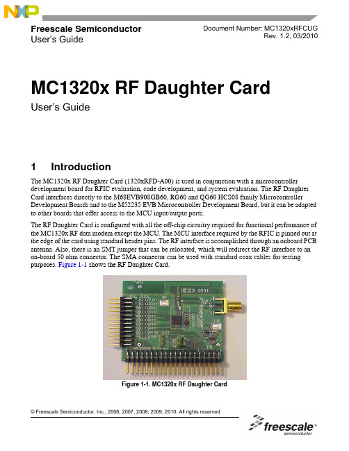
Freescale Semiconductor User’s GuideDocument Number: MC1320xRFCUGRev. 1.2, 03/20101IntroductionThe MC1320x RF Daughter Card (1320xRFD-A00) is used in conjunction with a microcontroller development board for RFIC evaluation, code development, and system evaluation. The RF Daughter Card interfaces directly to the M68EVB908GB60, RG60 and QG60 HCS08 family Microcontroller Development Boards and to the M52235 EVB Microcontroller Development Board, but it can be adapted to other boards that offer access to the MCU input/output ports.The RF Daughter Card is configured with all the off-chip circuitry required for functional performance of the MC1320x RF data modem except the MCU. The MCU interface required by the RFIC is pinned out at the edge of the card using standard header pins. The RF interface is accomplished through an onboard PCB antenna. Also, there is an SMT jumper that can be relocated, which will redirect the RF interface to an on-board 50 ohm connector. The SMA connector can be used with standard coax cables for testing purposes. Figure 1-1 shows the RF Daughter Card.Figure1-1. MC1320x RF Daughter CardMC1320x RF Daughter CardUser’s GuideIntroductionFigure1-2 shows the RF Daughter Card installed in a GB60 development board.Figure1-2. MC1320xRF Daughter Card In GB60 Development Board Figure1-3 shows the M52235 EVB development board.Figure1-3. M52235 EVB Development BoardSafety Information 2Safety InformationAny modifications to this product may violate the rules of the Federal Communications Commission and make operation of the product unlawful.47 C.F.R. Sec. 15.21This equipment has been tested and found to comply with the limits for a Class B digital device, pursuant to part 15 of the FCC Rules. These limits are designed to provide reasonable protection against harmful interference in a residential installation. This equipment generates uses and can radiate radio frequency energy and, if not installed and used in accordance with the instructions, may cause harmful interference to radio communications. However, there is no guarantee that interference will not occur in a particular installation. If this equipment does cause harmful interference to radio or television reception, which can be determined by turning the equipment off and on, the user is encouraged to try to correct the interference by one or more of the following measures:•Reorient or relocate the receiving antenna.•Increase the separation between the equipment and receiver.•Connect the equipment into an outlet on a circuit different from that to which the receiver is connected.•Consult the dealer or an experienced radio/TV technician for help.47 C.F.R. Sec.15.105(b)This equipment complies with FCC radiation exposure limits set forth for an uncontrolled environment. The antenna(s) used for this equipment must be installed to provide a separation distance of at least 8 inches (20cm) from all persons.This device complies with Part 15 of the FCC Rules. Operation is subject to the following two conditions:•This device may not cause harmful interference.•This device must accept any interference received, including interference that may cause undesired operation.3Revision HistoryThe following table summarizes revisions to this document since the previous release (Rev 1.1).Revision HistoryLocation RevisionSection 6Updated document cross reference.MC1320x MCU Interface4MC1320x MCU InterfaceFigure4-1 shows the typical connections between the MC1320x transceiver and a microcontroller unit (MCU). See the MC13202/203 Reference Manual, document MC13202RM, for interface considerations. Details about the interconnects for both the GB60 and M52235 Development boards are described in Section5.1, “Development Board Interconnects”. ArrayFigure4-1. MCU Interface PinoutDaughter Card Description 5Daughter Card DescriptionAs shown in Figure5-1 and Figure8-1, connector J101 is the main interface to the GB60 Development Board. The interface connections described in Section5.1, “Development Board Interconnects”, fall under the following three broad categories:1.Serial Peripheral Interface (SPI)2.Control3.PowerFigure1-2 shows how the RF Daughter Card is mounted on the GB60 Development Board.NOTEEnsure that zero ohm resistor R104 is in place on the MC1320x DaughterCard. As of this release, previous versions of the MC1320x Daughter Cardmay not have R104 inserted.NOTEJ101 Pin 1 of the MC1320x must to be connected to GB_PORT Pin 1 of theGB60 Development Board.As shown in Figure5-1 and Figure8-1, connector J102 is the main interface to the M52235 Development Board. Figure1-3 shows how the RF Daughter Card is mounted on the M52235 Development Board.NOTEJ102 Pin 1 of the MC1320x must be connected to MCU_PORT Pin 1 on theM52235 Development Board.Figure5-1 shows the top side of the RF Daughter Card PCB with component placement.Figure5-1. MC1320x Daughter Card (Top View)Daughter Card DescriptionFigure5-2 shows the shows the bottom side of the RF Daughter Card PCB.Figure5-2. MC1320x Daughter Card (Bottom View)5.1Development Board InterconnectsThe following sections describe the interconnects for both the GB60 and M52235 Development boards. Table5-1 lists the pin connections for J101 and Table5-2 lists the pin connections for J102.Table5-1. J101 Pin ConnectionsPin Number Pin Name Description Functionality1,2,3,4, 6,7,8,9, 10,11,12,15,16,17 18,21,23,25,26,28, 29, 30,33N/C No connection.5PTA2Connects to PTA2 on GB60.Provides a wakeup function to the MCU via Pin22 when jumper is installed between J103 pins1 and 2.13GPIO1Connects to General PurposeInput/Output 1 of MC1320X.When gpio_alt_en, Register 9, Bit 7 = 1, GPIO1 functions as an “Out of Idle” Indicator.14GPOI2Connects to General PurposeInput/Output 2 of MC1320X.When gpio_alt_en, Register 9, Bit 7 = 1, GPIO2 functions as a “CRC Valid” Indicator.Daughter Card Description19IRQConnects to IRQ pin of MC1320X.Allows the MC1320X to issue an IRQ to theMCU.20RESETOptionally connects to RESET of MC1320X when R101 or R102 are installed.Allows the MCU to reset the MC1320X.22PTE1/RXD1Connects to PTE1/RXD1 of GB60.Provides a wakeup function to the MCU via Pin5 when jumper is installed between J103 pins 1 and 2.24XCLK/16MHz Connects to CLKO of MC1320Xwhen jumper is installed between J103 pins 3 and 4.Provides reference based on MC1320X 16 MHz reference oscillator to the MCU.27PTC2/BAUD SEL Connect to PTC2/BAUD SEL ofGB60.31RXTXENConnect to RXTXEN of MC1320X.Allows the MCU to control the RXTXEN line ofthe MC1320X.32RESETConnects to RESET of MC1320X.Allows the MCU to reset the MC1320X.34PTD5/CESI/A TTN Connects to PTD5/CESI of GB60when R104 is installed. Connectdirectly to Pin 15 of J102.Allows the MCU to wake up the MC1320X from Doze or Hibernate.35MOSIConnect to MOSI of MC1320x.SPI36SPSCKConnect to SPICLK of the MC13201.SPI37CE Connect to CE of MC1320X.SPI38MISO Connects to MISO of MC1320X.SPI39V_INConnects the Daughter Card to the supply voltage output of the GB60 board.Provides supply voltage to the Daughter Card. Voltage must not exceed 16 Vdc. See Section 5.1.0.3, “Power Connections”.40GNDConnect ground on GB60 board to ground on Daughter Card.Table 5-1. J101 Pin Connections (continued)Pin NumberPin Name DescriptionFunctionalityDaughter Card DescriptionTable5-2. J102 Pin ConnectionsPin Number Pin Names Description Functionality 4, 5, 6, 7, 8, 11, 12, 14,16, 18, 22N/C No connection1V_IN Connects the Daughter Card to thesupply voltage output on theM52235EVB.Provides supply voltage to the Daughter Card. Voltage must not exceed 16 Vdc. See Section5.1.0.3, “Power Connections”.2IRQ Connects to IRQ pin of MC1320X.Allows the MC1320X to issue an IRQ to theMCU.3GND Connects the ground of the RFDaughter Card to the ground of theM52235EVB9GPIO1Connects to General PurposeInput/Output 1 of MC1320X.When gpio_alt_en, Register 9, Bit 7 = 1, GPIO1 functions as an “Out of Idle” Indicator.10GPOI2Connects to General PurposeInput/Output 2 of MC1320X.When gpio_alt_en, Register 9, Bit 7 =1, GPIO2 functions as a “CRC Valid” Indicator.13RESET Connects to RESET of MC1320Xand Pin 32 of J101.Allows the MCU to reset the MC1320X.15PTD5/CESI Connects to ATTN of MC1320Xand Pin 34 of J101.Allows the MCU to wake up the MC1320X from Doze or Hibernate.17MOSI Connects to MOSI of MC1320X.SPI19MISO Connects to MISO of MC1320X.SPI20RXTXEN Connect to RXTXEN of MC1320X.Allows the MCUntrol the RXTXEN line of theMC1320X.21SPICLK Connect to SPICLK of theMC1320XSPI23PTE2/CE-QSPI-CSO Connects to Pin 1 of J104Allows Chip Enable (CE) selection.See Section5.1.0.1, “SPI Connections”.24PTE2/CE-AN7Connects to Pin 3 of J104Allows Chip Enable (CE) selection.See Section5.1.0.1, “SPI Connections”.Daughter Card DescriptionNOTEIn the following sections, pin numbers not in parenthesis reference theGB60 Development Board. Pin numbers in parenthesis reference theM52235 Development Board.5.1.0.1SPI ConnectionsJ101 pins 35 through 38 (J102 pin 17, 19, 21 and 23) provide the following four wire SPI interface:•MOSI•SPICLK•CE•MISOThe MC1320x always functions as a slave device. SPI operation is described in detail in the appropriate MC1320x Data Sheet and/or MC1320x Reference Manual.NOTEAs it applies to the M52235 Development Board, the CE signal on (J102 Pin23 and Pin 24) are hard wired to header J104. These pins control thefunctionality of CE.When Pin 2 and Pin 3 of J104 are shorted, CE is wired to (J102 Pin 24)(PTE2/CE-AN7).When Pin 1 and Pin 2 of J104 are shorted, CE is wired to (J102 Pin 23)(PTE2/CE-QSPI_CS0).5.1.0.2Control Connections•J101 Pin 19 (J102 Pin 2) is the IRQ line from the MC1320x. Connection to the MCU depends on how the MCU services interrupts.•J101 Pin 31 (J102 Pin 20), RXTXEN, allows the MCU to initiate transceiver functions.•J101 Pin 34 (J102 Pin 15), ATTN, allows the MCU to wake up the MC1320x from Doze or Hibernate low power modes.NOTERXTXEN and ATTN are also available at header J105 for manual control.•J101 Pin 24 provides the MC1320x CLKO to the MCU when a jumper is installed at J103.•J101 Pin 32 (J102 Pin13) interfaces with the MCU to provide a Reset to the MC1320x.•J101 Pin 5 and Pin 22 provide a wake up function to the MCU when a jumper is installed at J103.•J101 Pin 13 and Pin 14 (J102 Pin 9 and Pin 11) provide access to the MC1320x GPIO1 and GPIO2 ports.RF Circuit5.1.0.3Power ConnectionsJ101 Pin 39 (J102 pin 1) provides the supply voltage to the RF Daughter Card. V oltage on this line should never exceed 16.0 VDC and the nominal voltage supply should not exceed 16.0 VDC. J101 Pin 40 (J102 pin 3) is ground.NOTEMCU connection signals are dependent on the on-board voltage regulator.If R105, D101, and C101 are mounted and R115 is removed, J101 Pin 39will provide the interface supply voltage which must never exceed 3.6 V.Nominal supply voltage should never exceed 3.4 V.5.1.0.4Non-MCU ConnectionsHeader J105 provides connections to a number of MC1320x contacts for non-MCU connections. As already stated, the RXTXEN and ATTN lines are available at J105 for external control using switches or other hardware. The MC1320x GPIO is also available for connection to external hardware.6RF CircuitThe MC1320x has an internal TX/RX switch. This feature allows for an external RF circuit that has a very low component count. The MC1320x requires only a few passive components and a balun to provide an interface to an antenna or a 50 ohm circuit. Figure6-1 shows a schematic for only the RF portion of the MC1320x Daughter Card.Figure6-1. RF Portion of 20x Daughter CardSoftware Configuration To provide a design that is of the lowest possible cost to produce, this reference design was built on a printed circuit board consisting of only two layers and with a printed circuit board antenna. The antenna is an Inverted F design widely used in the 2.4 GHz band. This antenna provides good performance while minimizing Bill of Material (BOM) cost.For more information on a low cost design approach, see the ZigBee Hardware Design Considerations Reference Manual (ZHDCRM)7Software ConfigurationAs shown in Figure8-1, the legend in the schematic shows the recommended jumper settings for Wake, ClkOut, and Chip Enable.NOTEThe Wake and ClkOut signals are only for interface to the GB60Development Board. The Chip Enable signal is only for interface to theM52235 Development Board.For software development, Freescale recommends users obtain the most recent software development tools and documentation from the following web pages:•For ZigBee related software and documentation go to /zigbee•For microcontroller software and documentation go to Bill of Materials (BOM) and Schematic8Bill of Materials (BOM) and Schematic This section contains the RF Daughter Card BOM and schematic.Table8-1. Bill of MaterialsQty Part Number ValueRatingToleranceManufacturer Part Number Reference196000310100Label 21*6mmTest BarCode96000310100BARCODE101350610710001100nF16V±10% X7R Murata GRM155R71C104KA88D C103, C104,C105050610710001100nF16V±10% X7R Murata GRM155R71C104KA88D C101 (NotMounted)2506208100011µF 6.3V±10% X5RMurata GRM188R60J105KA01D C102, C1060506208100011µF 6.3V±10% X5R Murata GRM188R60J105KA01D C108 (NotMounted)05061061000010nF16V±10% X7R Murata GRM155R71E103KZ01E C107(NotMounted)153300833001 3.3µF10V20%Vishay Sprague293D335X0010A2TE3C109250210268000 6.8pF50V±0.25pF NP0/C0GMurata GRM1555C1H6R8DZ01J C110, C11115021031000010pF50V±5% NP0/C0GMurata GRM1555C1H100JZ01D C112150210210000 1.0pF50V±0.25pF NP0/C0GMurata GRM1555C1H1R0CZ01D C113040110003303MM3Z3V3T1G 3.3V/200mW5%ONSemiconductorMM3Z3V3T1G D101 (NotMounted)141100017001Green_LED Citizen CL-170G-CD-T D102135501320200MC13202FreescaleSemiconductorMC13202IC101 134000298109LP2981IM5-3.3-40 to +125°C National LP2981IM5-3.3 NOPB IC1021200304040012*20p PinHeader - RightAnglemot/molex70216-4010-89-4402J1011200304024012*12p PinHeader - RightAnglemot/molex70216-2410-89-4242J1021200304004002*2p PinHeaderAMP0-826632-2J103 120030400300jumper_1x3AMP826629-3J104Bill of Materials (BOM) and Schematic200304020082*10 Pin HeaderAMP1-826632-0J105 (Not Mounted)120150700202SMA_edge_Re ceptacle_Fema lemot/sma-end_launch 142-0701-831J106220030000100ProbeLoop TobyElectronics TP-107-02-5-T J107, J108254710518001 1.8nH 300mA ±0.3nH TOKO LL1005-FHL1N8S L101, L102254710539002 3.9nH ±0.3nHTOKO LL1005-FHL3N9S L103, L104171000566010fsl566-1FreescaleSemiconductor FSL566-1 FR4 0.76mm PCB1014611000000010R 62.5mW/25V 5%YAGEO RC0402JRE070RL R103, R112, R115,R1040611000000010R62.5mW/25V 5%YAGEORC0402JRE070RLR101, R102 (NotMounted)061100410001100R 62.5mW/25V 5%YAGEO RC0402JRE07100RL R105 (Not Mounted)06110061000110K62.5mW/25V 5%YAGEORC0402JRE0710KLR106, R107, R108, R110 (NotMounted)161100747000470K 62.5mW/25V 5%YAGEO RC0402JRE07470KL R109161100422000220R 62.5mW/25V 5%YAGEO RC0402JRE07220RL R1111611200000010R 125mW/150V 5%YAGEO RC0805JRE070RL R1130611200000010R 125mW/150V 5%YAGEO RC0805JRE070RL R114 (Not Mounted)15813091600416.000MHz ±20ppm ±20ppmKDS ZD00882X101156360240001LDB212G4005C-001MurataLDB212G4005C-001Z101Table 8-1. Bill of MaterialsQty Part Number Value Rating ToleranceManufacturer Part Number ReferenceNOTESHow to Reach Us:Home Page:E-mail:*********************USA/Europe or Locations Not Listed:Freescale SemiconductorTechnical Information Center, CH3701300 N. Alma School RoadChandler, Arizona 85224+1-800-521-6274 or +1-480-768-2130*********************Europe, Middle East, and Africa:Freescale Halbleiter Deutschland GmbHTechnical Information CenterSchatzbogen 781829 Muenchen, Germany+44 1296 380 456 (English)+46 8 52200080 (English)+49 89 92103 559 (German)+33 1 69 35 48 48 (French)*********************Japan:Freescale Semiconductor Japan Ltd.HeadquartersARCO Tower 15F1-8-1, Shimo-Meguro, Meguro-ku,Tokyo 153-0064, Japan0120 191014 or +81 3 5437 9125***************************Asia/Pacific:Freescale Semiconductor Hong Kong Ltd.Technical Information Center2 Dai King StreetTai Po Industrial EstateTai Po, N.T., Hong Kong+800 2666 8080**************************For Literature Requests Only:Freescale Semiconductor Literature Distribution Center P.O. Box 5405Denver, Colorado 802171-800-521-6274 or 303-675-2140Fax: 303-675-2150*********************************************Information in this document is provided solely to enable system and software implementers to use Freescale Semiconductor products. There are no express or implied copyright licenses granted hereunder to design or fabricate any integrated circuits or integrated circuits based on the information in this document.Freescale Semiconductor reserves the right to make changes without further notice to any products herein. Freescale Semiconductor makes no warranty, representation or guarantee regarding the suitability of its products for any particular purpose, nor does Freescale Semiconductor assume any liability arising out of the application or use of any product or circuit, and specifically disclaims any and all liability, including without limitation consequential or incidental damages. “Typical” parameters that may be provided in Freescale Semiconductor data sheets and/or specifications can and do vary in different applications and actual performance may vary over time. All operating parameters, including “Typicals”, must be validated for each customer application by customer’s technical experts. Freescale Semiconductor does not convey any license under its patent rights nor the rights of others. Freescale Semiconductor products are not designed, intended, or authorized for use as components in systems intended for surgical implant into the body, or other applications intended to support or sustain life, or for any other application in which the failure of the Freescale Semiconductor product could create a situation where personal injury or death may occur. Should Buyer purchase or use Freescale Semiconductor products for any such unintended or unauthorized application, Buyer shall indemnify and hold Freescale Semiconductor and its officers, employees, subsidiaries, affiliates, and distributors harmless against all claims, costs, damages, and expenses, and reasonable attorney fees arising out of, directly or indirectly, any claim of personal injury or death associated with such unintended or unauthorized use, even if such claim alleges that Freescale Semiconductor was negligent regarding the design or manufacture of the part.Freescale™ and the Freescale logo are trademarks of Freescale Semiconductor, Inc. All other product or service names are the property of their respective owners.© Freescale Semiconductor, Inc. 2006, 2007, 2008, 2009, 2010. All rights reserved.。
半导体测试系统

YB6500高速多用途半导体分立器件测试系统广泛应用于航天、航空、兵器、中船、电子多个领域,以产品性价比好、可测器件和参数齐全、测试精度高、速度快、保护性强、稳定性可靠性高、故障率极低、软件丰富、操作使用方便、售后服务为宗旨。
1、电学指标A-K 极间加压范围: ±2.500mV--2000V A-K 极间测流范围: ±1nA--49.90AA-K 极间加流范围: ±100nA--49.90AA-K 极间测压范围: ±2.500mV--2000VG-K 极间加压范围: ±2.500mV--20VG-K 极间测流范围: ±1nA--10AG-K 极间加流范围: ±100nA--10AG-K 极间测压范围: ±2.500mV--20V最大电压分辨率: 1mV最大电流分辨率: 1nAA-K 极间加/测压精度: 1%+10mVA-K 极间加/测流精度: 1%+10nA+20pA/VG-K 极间加/测压精度: 1%+5mVG-K 极间加/测流精度: 1%+10nA+20pA/V电参数测试重复性: 1%2、可测试器件(DUT)种类共计19大类, 27分类分立器件。
序号类型名称符号1 二极管DIODE2 稳压(齐纳)二极管ZENER3 晶体管TRANSISTOR(NPN/PNP)4 单向可控硅(普通晶闸管)SCR5 双向可控硅(双向晶闸管)TRIAC6 金属-氧化物-半导体场效MOSFET(N-CH/P-CH)应管7 结型场效应管J-FET(N-CH/P-CH)8 绝缘栅双极大功率晶体管IGBT(N-CH/P-CH)9 达林顿阵列器件DARLINGTON10* 光电耦合器OPTO-COUPLER(NPN/PNP)11* 光电逻辑器件OPTO-LOGIC12* 光电开关管OPTO-SWITCH13* 固态过压保护器SSOVP14* 硅触发开关STS,SBS15* 继电器RELAY(A,B,C型)16* 金属氧化物压变电阻MOV17* 压变电阻VARISTOR18* 双向触发二极管DIAC19* 三端稳压器REGULATOR* 需要另行定制专门的测试适配器和测试夹具。
广芯微电子 EFT 测试操作手册说明书

AN0101应用笔记EFT测试操作手册版本:V1.2广芯微电子(广州)股份有限公司/AN0101条款协议条款协议本文档的所有部分,其著作产权归广芯微电子(广州)股份有限公司(以下简称广芯微电子)所有,未经广芯微电子授权许可,任何个人及组织不得复制、转载、仿制本文档的全部或部分组件。
本文档没有任何形式的担保、立场表达或其他暗示,若有任何因本文档或其中提及的产品所有资讯所引起的直接或间接损失,广芯微电子及所属员工恕不为其担保任何责任。
除此以外,本文档所提到的产品规格及资讯仅供参考,内容亦会随时更新,恕不另行通知。
1. 本文档中所记载的关于电路、软件和其他相关信息仅用于说明半导体产品的操作和应用实例。
用户如在设备设计中应用本文档中的电路、软件和相关信息,请自行负责。
对于用户或第三方因使用上述电路、软件或信息而遭受的任何损失,广芯微电子不承担任何责任。
2. 在准备本文档所记载的信息的过程中,广芯微电子已尽量做到合理注意,但是,广芯微电子并不保证这些信息都是准确无误的。
用户因本文档中所记载的信息的错误或遗漏而遭受的任何损失,广芯微电子不承担任何责任。
3. 对于因使用本文档中的广芯微电子产品或技术信息而造成的侵权行为或因此而侵犯第三方的专利、版权或其他知识产权的行为,广芯微电子不承担任何责任。
本文档所记载的内容不应视为对广芯微电子或其他人所有的专利、版权或其他知识产权作出任何明示、默示或其它方式的许可及授权。
4. 使用本文档中记载的广芯微电子产品时,应在广芯微电子指定的范围内,特别是在最大额定值、电源工作电压范围、热辐射特性、安装条件以及其他产品特性的范围内使用。
对于在上述指定范围之外使用广芯微电子产品而产生的故障或损失,广芯微电子不承担任何责任。
5. 虽然广芯微电子一直致力于提高广芯微电子产品的质量和可靠性,但是,半导体产品有其自身的具体特性,如一定的故障发生率以及在某些使用条件下会发生故障等。
此外,广芯微电子产品均未进行防辐射设计。
测试设备说明手册(TESTO)说明书

testo 830-T1 (0560 8311) testo 830-T2 (0560 8312)91. General Information Please read this document through carefully and familiarise yourself with the operation of the product before putting it to use.Keep this documentation to hand so that you can refer to it when necessary.2. Product Description3. Safety InformationContact measurement: Do not measure on or near live parts. Infrared measurement: Please adhere to the required safe distance when measuring on live parts.Operate the instrument properly and according to its intended purpose and within the parameters specified. Do not use force.Do not expose to electromagnetic radiation (e.g. microwaves,induction heating systems), static charge, heat or extreme fluctuations in temperature.Do not store together with solvents (e.g. acetone).Open the instrument only when this is expressly described in the documentation for maintenance purposes.Laser radiation! Do not look into laser beam. e n Accessories Name Item no.Water-tight immersion/penetration probe, -60 to +400°C/-76 to +752°F 0602 1293Quick-reaction surface probe, -60 to +300°C/-76 to +572°F 0602 0393Robust air probe, -60 to +400°C/-76 to +752°F 0602 1793Leather protection sleeve 0516 8302Emissivity adhesive tape ε=0.950554 0051Infrared sensor,laser Battery compartment DisplayOn/Off switch Contact measurement Measurement button:infrared measurement Infrared measurementProbe socket (testo 830-T2 only)10Ensure correct disposal:Dispose of defective rechargeable batteries and spentbatteries at the collection points provided.Send the instrument directly to us at the end of its life cycle.We will ensure that it is disposed of in an environmentallyfriendly manner.4. Intended Usetesto 830 is a compact infrared thermometer for the non-contact measurement of surface temperatures. Using testo830-T2, it is possible to carry out additional contact measurements byattaching probes.5. Technical DataFeature testo 830-T1testo 830-T2Parameter°C/°FInfrared measurement range-30 to +400°C/ -22 to +752°FInfrared resolution0.1°C/0.1°FInfrared accuracy±1.5°C/ 2.7°F or 1.5% of reading (+0.1 to +400°C/ +32 to +752°F)1;(at 23°C) +/- 1 digit±2°C/ 3.6°F or 2% of reading (-30 to 0°C/ -22 to +31.9°F)1Emissivity0.1 to 1.0 adjustableInfrared measurement rate0.5sTemp. sensor -Thermocouple Type K (attachable) Measurement range of temp sensor--50 to +500°C/ -58 to +932°F Resolution of temp. sensor-0.1°C/ 0.1°FAccuracy of temp. sensor-±0.5°C/0.9°F+0.5% of reading (±1 digit)at rated temperature 22°C/ 72°F Measuring rate of temp. sensor- 1.75sOptics (90% value)10:1212:12Laser type 1 x laser 2 x laserOperating temperature-20 to +50°C/ -4 to +122°FTransport /S torage temperature-40 to +70°C/ -40 to +158°FPower supply9V block batteryBattery life 20 h 15 hHousing ABSDimensions (LxHxB)190 x 75 x 38mm/ 7.5 x 3.0 x 1.5inCE guideline2004/108/EECWarranty 2 yearsLaserLaser type 1 x laser 2 x laserPower< 1 mWWavelength645 to 660 nmClass2Standard DIN NE 60825-1:2001-111the larger value applies2+ Opening diameter of the sensor (16mm/ 0.6in)6. Initial OperationInsert battery: See 9.1Changing the battery.117. Operation7.1 Connecting probe (testo 830-T2 only)Connect temperature probe to probe socket. Observe +/-!7.2 Switching on/offSwitch on instrument: Press measurement button.-lights up).The display light remains for 10 seconds every time a button is activated.pressed until display darkens.The device switches off automatically after 1 min (IR measure -ment view) or 10 mins (contact measurement view, only testo830-T2) without the button being pressed.7.3 Measuring/ measurement, this is done when the device is switched off orwhen you switch to the IR measurement view.-The instrument is switched on.Infrared measurement1Start measurement: Hold down measurement button.2Locate object to be measured using laser point.testo830-T1: laser marks the centre point of the measurement spot.testo830-T2: Laser marks the upper and lower end of themeasurement spot.-The current reading is shown (2 measurements per second)3End measurement: Release button.-HOLD lights up. The last measured value and min./max. value are saved until the next measurement.Restart measurement: Press measurement button.Contact measurement (testo 830-T2 only)-Temperature probe was connected before the measuring instrument was switched on.1-The instrument changes to the contact measurement mode (lights up). The current reading is shown.en122End the measurement: Press .-HOLD lights up. The last measured value and min./max. value are saved until the next measurement.Switch between min., max. and recorded value: Press .Restart measurement: Press .Back to infrared measurement view: Press measurementbutton.Setting the emissivity-Instrument is in the infrared measurement mode.If no button is pressed for 3 s in the emissivity mode, theinstrument switches to the infrared measurement mode.1Press for 3 s.2Set emissivity: Press or-The instrument switches to the infrared measurement mode.8. Settings-Instrument is switched off.If no button is activated in the setting mode for 3 s, theinstrument changes to the next mode.1Press for 3 s.-The device switches to settings mode.2Set lower alarm value (ALARM): Press or . Hold the button down to go forward quickly.3Set upper alarm value (ALARM): Press or . Hold the button down to go forward quickly.4Set alarm function on/oFF: Press or .5Select parameter (°C/ °F) : Press or .-The device returns to IR measurement view.The alarm function is only available for IR measurement. If theset alarm values are exceeded/not reached, a visual andacoustic alarm is output.9. Service and Maintenance9.1 Changing the batteryInstrument must be switched off!1Open battery compartment:Open up cover.2Remove used battery and insert newone. Observe +/-. The minus should bevisible once the battery is inserted.3Close battery compartment: Closecover.139.2 Clean instrument Do not use abrasive cleaning agents or solutions.Clean the housing with a damp cloth (soap water).Carefully clean the lens with water or cotton buds dipped in water or medical alcohol. 10. Questions and AnswersQueryPossible causes Possible solutionInfrared measurement mode: -Readings outside -- - -lights up.measurement range.Contact measurement mode: -Readings outside -If we have not answered your question, please contact your local distributor or Testo´s Customer Service.11. Information on infrared measurement 11.1 Measurement methodInfrared measurement is an optical measurementKeep lens clean.Do not measure with clouded lens.Keep measurement field (area between instrument and object being measured) free of interferences: no dust and dirtparticles, no moisture (rain, steam) or gases.Infrared measurement is a surface measurementIf there is dirt, dust, frost etc. on the surface, only the top layer will be measured, i.e. the dirt.In the case of shrinkwrapped foodstuffs, do not measure in air pockets.If values are critical, always subsequently measure using a contact thermometer. Particularly in the food sector, the core temperature should be measured with a penetration/immersion thermometer.Adaptation timeIf the ambient temperature changes (change of location, e.g.inside/outside measurement) the instrument needs an adaptation time of 15 minutes for infrared measurement.e n1411.2 EmissivityMaterials have different emissivities, i.e. they emit different levels of electromagnetic radiation. The emissivity of testo 830 is set in the factory to 0.95. This is the ideal value for measuring non-metals (paper, ceramics, plaster, wood, paints and varnishes),plastics and foodBright metals and metal oxides are only suited to a limited extent to infrared measurement on account of their low or nonuniform emissivity.Apply emissivity enhancing layers such as varnish or emission adhesive tape (Item no. 05540051) to the object being measured. If this is not possible, measure with the contact thermometer.Emissivity table of the most important materials(typical values)A specific spot is determined depending on the distance from the measuring instrument to the object being measured. Measurement optics (Ratio Distance : Measurement spot)500 mm1000 mm2000 mm5000 mmØ 516 mmØ 216 mmØ 116 mmØ 66 mmØ 16 mm testo 830-T1laser1512. Information on contactmeasurementObserve minimum penetration depth in immersion/penetration probes: 10 x probe diameterAvoid applications in corrosive acids or bases.Do not use spring-loaded surface probes on sharp edges.e n 500 mm 1000 mm2000 mm 5000 mm Ø 433 mm Ø 183 mmØ 100 mmØ 58 mm Ø 16 mm testo 830-T2laserlaser。
Keysight B1500A半导体器件简化配置流程说明书

¨ B1500A-015 for 1.5m ¨ B1500A-030 for 3.0m
¨ B1500A-A01 Standard
package (4 MPSMUs + cables)
¨ B1500A-A02 High
resolution package (4 HRSMUs + cables)
¨ B1500A-A03 High power
– B1500A, B1500A-015 – B1500A-A00 – B1500A-A17 2ea. – B1500A-A5F
This information is subject to change without notice. © Keysight Technologies, 2010 – 2014, 2016 Published in USA, February 25, 2016 5990-5837EN
Table 2. Other accessories
Resource B1542A N1301A N1301A-100 N1301A-102 N1301A-110 B1542A
Description Ultra short pulsed IV package CMU accessories for B1500A SCUU (SMU CMU Unify Unit) SCUU cable (3m) SCUU magnetic stand Ultra short pulsed IV package
3 Please contact your local Keysight office to find out which WGFMU add-on package fits to your requirements. The complete contact list is available at /find/contactus
LX9300-大功率分立器件测试系统doc

LX9300 大功率分立器件测试系统系统用途LX9300大功率分立器件测试系统是由北京励芯泰思特测试技术有限公司自主研制、开发、生产的半导体参数测试的专用设备, 本测试系统不仅满足大功率VDMOS 的GFS(跨导)测试、IGBT功率参数的测试,还涵盖中小功率半导体器件的测试,适用于半导体器件生产厂家进行圆片中测或封装成测,各类整机厂家、科研院所的质量检测部门进行入厂检验、可靠性分析测试测试原理符合《GJB 128 半导体分立器件试验方法》、《GJB 33A-97 半导体分立器件总规范》《SJ/Z 9014 半导体器件分立器件》、《SJ 2215.1-82半导体光耦器测试方法》等相应的国家标准、国家军用标准。
系统的人机界面有好,编程容易,软件能对用户输入的数据进行自动查错。
系统软件可进行器件参数的分档、分类编程,并可实时显示和记录分档、分类测试结果,测试结果和统计结果均可以用EXCEL格式存贮于计算机中,根据需要可以打印输出。
系统为模块化、开放式结构,具有升级扩展潜能。
系统特点◆PC机为系统的主控机◆菜单式测试程序编辑软件操作简便◆预先连接测试自动识别NPN/PNP◆ 0~±2000V程控高压源◆高达±500A程控高流源(可扩展到±1000A)◆±40V/±40A(可扩展到±80V、±50A)的可编程电压电流源通过测试系统先进的硬件闭环测试方法实现功率VDMOS的GFS跨导的测试◆测试漏流最小分辨率达6.1pA◆四线开尔文连接保证加载测量的准确◆通过IEEE488接口连接校准数字表传递国家计量标准对系统进行校验◆ Prober接口、Handler接口可选(16Bin)◆可为用户提供丰富的测试适配器测试对象二极管/稳压管/恒流二极管/整流桥/瞬态抑制管:BVR、IR、VF、VZ、RZ三极管:BVCBO、BVCEO、BVCES、BVCER、BVEBO、HFE、ICBO、ICBS、ICEO、ICES、ICER、IEBO、VBEF、VBCF、VBESAT、VCESAT可控硅:BVGKO、IAKF、IAKR、IGKO、IGT、IH、IL、VGT、VON场效应管: BVDSO、BVDSS、BVDSR、BVDGO、BVGDS、BVGSO、BVGSS、GFS、IDSO、IDSS、IDSR、IG、IGDO、IGSO、IGSS、RDS(on)、VDS(on)、VGS、VGS(th)、VPIGBT:BVCES、BVCGR、BVGES、ICES、IGES、VCESAT、VGETH、VGS(off) 达林顿矩阵:ICEX、IIN(ON)、IIN(Off)、VIN(on)、IR、VCESA T、BVR、HFE、ICEO单结晶体管:Iv、Vv、IP、VP、VEB1、ETA、RBB、IEB1O、IB2光敏二、三极管:ID、IL、VOC、ISC、BV、BVCE光耦:C TR、BVECO、BVCBO、BVCEO、ICBO、ICEO、HFE、VBESAT、VCESAT、IR、IAKF、IAKR技术指标1. 电流/电压源P VIS2. 数据采集VM16位ADC,100K/S采样速率。
某半导体分立器件封装测试厂厂务能源管理系统介绍

2
N2
Bulk nitrogen tank, purity not less than 99.999%, Dew point -60℃, Oxygen less than 10PPM
Taida Low Temperature Equipment Co., Ltd.
3
H2
Cylinder, purity not less than 99.999%, Dew point 60℃, Oxygen less than 10PPM
4
IEHS/FSD Cost Reduction Plan
Energy supply specification
No.
1 2 3
Item
Type
3 phase 380VAC 1phase 220VAC 3 phase 380V EPS
Specification
50Hz, 3 phase 380V,±10% 50Hz, 1phase 220V, ±10% 50Hz,3 phase 380V,±10%
Taida Low Temperature Equipment Co., Ltd.
4
Tap water
P≥0.3MPa,quality to meet relevant standard of drinking water quality
Municipal Utility Service
Municipal Utility pipeline
Range of Supply
All building (Except for office) All building Fire fighting, EPS, exhaust scrubber system
- 1、下载文档前请自行甄别文档内容的完整性,平台不提供额外的编辑、内容补充、找答案等附加服务。
- 2、"仅部分预览"的文档,不可在线预览部分如存在完整性等问题,可反馈申请退款(可完整预览的文档不适用该条件!)。
- 3、如文档侵犯您的权益,请联系客服反馈,我们会尽快为您处理(人工客服工作时间:9:00-18:30)。
QTEC-4000 半导体分立器件测试系统说明书
1 . 2 . 5 . 4 S E L P I N : 用于扫描器时(S C A N N E R )设定管脚排列(P i n )。 1.2.5.4.1 S,B,C(K),E(A)输入器件的管脚(Pin)对应编号。如 B=2、 C=3、 E=1,则设定为 SCANNER 的 1 脚为 E 端,2 脚为 B 端,3 脚 为 C 端。
拣”设置)。 1.2.4.2.3.2.2 Logging Disappear: 显示器件的测试结果时不显示此项
目的测试结果。 1.2.4.2.3.2.3 Result Color Blue: 器件测试不通过时,测试结果用蓝色。 1 . 2 . 4 . 2 . 3 . 2 . 4 K e e p F o r c i n g : 保持加载。 1.2.4.2.3.3 标记: 修改各设定值(Limit Min / Limit Max / Bias)的
1 . 文 件 / 新 建 建立新的测试文件 2 . 测 试 项 / 新 增 测试项目的输入 3 . 分 类 项 / 新 增 分类项目的输入 4 . 文 件 / 保 存 保存编辑好的文件
8
QTEC-4000 半导体分立器件测试系统说明书
4. 条件: 作各 Bias 的设定,输入电流、输入电压等的条件值。 5. 时间 : 设定加载/测试时间。可以使用系统的默认值。用户也可以根据器件
的不同及测试的需要自行设定。(注:若测试项的电流值小于 100uA 时,时间 应大于 8ms. 若测试项的电流值小于 200mA 时,时间应小于 1ms) 6. 反转极性: 器件的极性反转(NPN 或者 PNP)。 7. 编 辑 明 细 : 测试项目的详细设定窗口。 8. 点击“ 确 定 ” 确认测试项目的各条件设定的输入。
试。 1.2.4.2.3.1.3 Sampling 1.1ms: 耐压测试时振荡对策,BV 测试的防止振
荡。 1 . 2 . 4 . 2 . 3 . 1 . 4 停 止 时 间 : 延迟加载电流或电压的时间。 1 . 2 . 4 . 2 . 3 . 1 . 5 进 行 时 间 : 加载电流或电压的时间。 1 . 2 . 4 . 2 . 3 . 1 . 6 各机能的详细说明,请参照硬件手册。 1 . 2 . 4 . 2 . 3 . 2 选 择 : 设定各项功能。也可以通过“测量/设置”同时设定。 1.2.4.2.3.2.1 Oscillation Invalidation: 器件振荡分类失效(参考“分
1.1.2 测试项目菜单
菜单内容
操作指令含义
新增
增加测试项目
修改
修改测试项目
插入
插入测试项目
删除
删除测试项目
复制块
批量拷贝测试项目
删除块
批量删除测试项目
反转极性
批量测试项目极性反转
替换
替换已有的测试项目
设置跳转
测试项目整体跳转设定
功能设置
各功能的整体设定
打印
打印测试文件
打印预览
预览打印文件
打印机设置
打印机的设定
退出
退出正在运行的 Editor
注: 保存已下载到测试主机中的文件时, 测试主机会自动下载保存后的程序。故在保存此类
文件之前需确认测试程序不在使用的状态。
4
QTEC-4000 半导体分立器件测试系统说明书
ADD
加法
Value1+Value2
DELTA
减法 Value1-Value2
MULTI
乖法
Value1*Value2
DIVID
除法
Value1/Value2
11
QTEC-4000 半导体分立器件测试系统说明书
1 . 2 . 5 . 2 S a m e : 测试结果参照项目,用于器件分类。
操作指令含义 增加分类项目 修改分类项目 插入分类项目 删除分类项目
键盘快捷键 Ctrl + W Ctrl + X Ctrl + Y Ctrl + Z
鼠标的快捷操作
鼠标左键双击修改处
5
QTEC-4000 半导体分立器件测试系统说明书
1.2. 测试文件的编写 1.2.1 文件编写的基本顺序:
QTEC-4000 半导体分立器件测试系统说明书
QTEC-4000 半导体分立器件测试系统
软件说明书
1
QTEC-4000 半导体分立器件测试系统说明书
目 录
1 EDITOR 使用
9
QTEC-4000 半导体分立器件测试系统说明书
1 . 2 . 4 . 2 . 3 时 间 : 设定加载时间。 1 . 2 . 4 . 2 . 3 . 1 整 个 循 环 : 设置做积分回路设定。
1 . 2 . 4 . 2 . 3 . 1 . 1 N o n e : 不动作。 1.2.4.2.3.1.2 Sampling 22ms: 切断电流测试结果安定化,稳定漏电流测
Ctrl + N
打开
打开已有的测度文件
Ctrl + O
保存
保存编辑完成的文件
Ctrl + S
另保存
将编辑的文件以其他的名称保存
打开暂存文件 打开暂时保存的文件
保存暂存文件 保存暂时的文件
编辑文件头信息 编辑测试文件信息
密码
文件保护密码的设定
设置并行测试点 设置双机并行时同一个器件进行分时测试,以提 高测试速度
2 Logger 使用说明 3 Opener 使用
键盘快捷键 Ctrl + R Ctrl + S Ctrl + I Ctrl + U Ctrl + V Ctrl + W Ctrl + X Ctrl + Y
鼠标的快捷操作
鼠标左键双击修改处
1.1.3 分类项菜单
菜单内容 新增 修改 插入 删除
1.2.4.2 测试项目详细设定窗口
1 . 2 . 4 . 2 . 1 项 目 名 称 : 用户可以根据需要,修改测试项目的显示名称。 1.2.4.2.2 分支: 满足分类的条件(测试通过/失败)时,程序直接跳转到指定测
试项目或直接分类,这样可以缩短测试时间。如输入数字,表示程序直 接到此编号的测试项目。如输入“SORT ”,表示程序跳转到分类项目直接 进行分类操作。“分支”设定也可用“项目/设置/跳转”菜单命令,为所 有的测试项目同时设定。 注: 通常“失败”时中断测试,直接分类。通过跳转,可以做详细的分 支设定。
正负极性。 1.2.5.特殊测试项目的使用
1 . 2 . 5 . 1 计 算 项 目 : 计算测试结果,在测试项目编号前加“# ”。例: # 2 。 如不加# ,系统将编号默认为数值。
10
QTEC-4000 半导体分立器件测试系统说明书
项目名称
项目说明
项目含义
1.2.5.2.1 数值中的 M#输入测试项目编号,以编号表示测试项目参照结果进行 分类。不再进行测试。(M # 显示中不用加# )
1 . 2 . 5 . 3 测试延迟(D E L A Y )。 1 . 2 . 5 . 3 . 1 时 间 : 输入需要延迟的时间。
2
QTEC-4000 半导体分立器件测试系统说明书
1.EDITOR 使用
点击 PEditor 图标 打开 Editor 主界面
1.1 菜单说明:
3
QTEC-4000 半导体分立器件测试系统说明书
1.1.1 文件菜单
菜单项
说 明
键盘快捷键
新建
新建测试文件
7
1.2.4 测试项目的设定窗口
QTEC-4000 半导体分立器件测试系统说明书
1.2.4.1 测量: 测量结果设定 1. 下限/上限: 测试通过值的最小/最大范围设定。(注:(注:为了较为准确测 量器件,下限/上限的选择应尽量接近器件的实际值)。 2. 测 量 范 围 : 可以设定量程 (1) 指定测试结果的量程。默认状态是 Max Limit。如果不设定 Max Limit 时,必须要选择一个测量的范围。这时一般设为正常数据的最大档位。 (2) 如测试量程设定在 1.000 时,数据的显示范围在 0.000 到 9.999。 (3) 测每个测试项目都改变量程不方便,因此通常“测量范围”都设定在 M a x L i m i t 。 3. 调整范围: 变动档位测试,测试精度可达 4 位。 (1) Off: 关闭自动变档,用 Logging 强制设定例外。 (2) Standard: 如果实测值超出量程,则自动将量程升一档。 (3) Limit Rage: 在限定的档位内变动。 (4) Invalidation: 自动变档禁止,即使用已定的强制设定也不动作。 (5) 使用该项功能时会影响测试时间,通常设定为 Off。
换器件管脚与测试盒的连接。 6. 检 查 汇 总 , 载 入 测 试 文 件 : 检查语法,并将测试文件下载到测试主机。 7. 点击“确定”确认设定项的输入。
6
1.2.3 测试项目的输入
QTEC-4000 半导体分立器件测试系统说明书
1. 项目名称: 可以直接用键盘输入要测试项目的名称,或者从项目列表中用鼠标选 取所需的项目。 2. 种 类: 供使用者选择测试器件的类型。系统默认为所有的类型的测试参数, 如果选取种类为晶体管时 ,那么在项目列表中只出现与三极管测试有关的测试参 数,其它类型器件参数将不再显示。 3. 项目表: 显示可供选择的器件测试参数。可以用鼠标点取需要的测试参数项目。 4. 特殊项目表: 在测试中需要用到的特殊项目。包括: 连接测试项、测试项四则运 算、用于参数分类的项目、Scaner 用管脚连接设定项目、阻抗器件震荡的测试、 三极管击穿电压的项目、器件管脚短接项目等内容。