数字集成电路(电路系统与设计)第3章习题
人邮社数字电路逻辑设计习题答案
习题参考解答第1章基本知识1.什么是数字信号?什么是模拟信号?(注:所有蓝色标题最后均去掉!)答案:数字信号:指信号的变化在时间上和数值上都是断续的,或者说是离散的,这类信号有时又称为离散信号。
例如,在数字系统中的脉冲信号、开关状态等。
模拟信号:指在时间上和数值上均作连续变化的信号。
例如,温度、交流电压等信号。
2.数字系统中为什么要采用二进制?答案:二进制具有运算简单、物理实现容易、存储和传送方便、可靠等优点。
3.机器数中引入反码和补码的主要目的是什么?答案:将减法运算转化为加法运算,统一加、减运算,使运算更方便。
4.BCD码与二进制数的区别是什么?答案:二进制数是一种具有独立进位制的数,而BCD码是用二进制编码表示的十进制数。
5.采用余3码进行加法运算时,应如何对运算结果进行修正?为什么?答案:两个余3码表示的十进制数相加时,对运算结果修正的方法是:如果有进位,则结果加3;如果无进位,则结果减3。
为了解决四位二进制运算高位产生的进位与一位十进制运算产生的进位之间的差值。
6.奇偶检验码有哪些优点和不足?答案:奇偶检验码的优点是编码简单,相应的编码电路和检测电路也简单。
缺点是只有检错能力,没有纠错能力,其次只能发现单错,不能发现双错。
7.按二进制运算法则计算下列各式。
答案:(1)110001 (2)110.11 (3)10000111 (4)1018.将下列二进制数转换成十进制数、八进制数和十六进制数。
答案:(1)(117)10 ,(165)8 ,(75)16(2)(0.8281)10 ,(0.65)8 ,(0.D4)16(3)(23.25)10 ,(27.2)8 ,(17. 4)169.将下列十进制数转换成二进制数、八进制数和十六进制数(精确到二进制小数点后4位)。
答案:(1)(1000001)2 ,(101)8 ,(41)16(2)(0.0100)2 ,(0.20)8 ,(0.40)16(3)(100001.0101)2 ,(41.24)8 ,(21.50)1610.写出下列各数的原码、反码和补码。
《数字电子技术基础》课后习题答案
《数字电路与逻辑设计》作业教材:《数字电子技术基础》(高等教育出版社,第2版,2012年第7次印刷)第一章:自测题:一、1、小规模集成电路,中规模集成电路,大规模集成电路,超大规模集成电路5、各位权系数之和,1799、,,;,,二、1、×8、√10、×三、1、A4、B练习题:1.3、解:(1) 十六进制转二进制: 4 5 C0100 0101 1100二进制转八进制:010 001 011 1002 13 4十六进制转十进制:(45C)16=4*162+5*161+12*160=(1116)10所以:(45C)16=(10001011100)2=(2134)8=(1116)10(2) 十六进制转二进制: 6 D E . C 80110 1101 1110 . 1100 1000 二进制转八进制:011 011 011 110 . 110 010 0003 3 3 6 . 6 2十六进制转十进制:(6DE.C8)16=6*162+13*161+14*160+13*16-1+8*16-2=(1758.78125)10 所以:(6DE.C8)16=(0. 11001000)2=(3336.62)8=(1758.78125)10(3) 十六进制转二进制:8 F E . F D1000 1111 1110. 1111 1101二进制转八进制:100 011 111 110 . 111 111 0104 3 7 6 . 7 7 2十六进制转十进制:(8FE.FD)16=8*162+15*161+14*160+15*16-1+13*16-2=(2302.98828125)10 所以:(8FE.FD)16=(1.11111101)2=(437 6.772)8=(2302.98828125)10(4) 十六进制转二进制:7 9 E . F D0111 1001 1110 . 1111 1101二进制转八进制:011 110 011 110 . 111 111 0103 6 3 6 . 7 7 2十六进制转十进制:(79E.FD)16=7*162+9*161+14*160+15*16-1+13*16-2=(1950. )10 所以:(8FE.FD)16=0.11111101)2=(3636.772)8=(1950.98828125)101.5、解:(74)10 =(0111 0100)8421BCD=(1010 0111)余3BCD(45.36)10 =(0100 0101.0011 0110)8421BCD=(0111 1000.0110 1001 )余3BCD(136.45)10 =(0001 0011 0110.0100 0101)8421BCD=(0100 0110 1001.0111 1000 )余3BCD (374.51)10 =(0011 0111 0100.0101 0001)8421BCD=(0110 1010 0111.1000 0100)余3BCD1.8、解(1)(+35)=(0 100011)原= (0 100011)补(2)(+56 )=(0 111000)原= (0 111000)补(3)(-26)=(1 11010)原= (1 11101)补(4)(-67)=(1 1000011)原= (1 1000110)补。
1篇3章习题解答浙大版集成电路课后答案

第三章场效应晶体管及其电路分析题1.3.1绝缘栅场效应管漏极特性曲线如图题1.3.1(a)~(d)所示。
(1)说明图(a)~(d)曲线对应何种类型的场效应管。
(2)根据图中曲线粗略地估计:开启电压V T、夹断电压V P和饱和漏极电流I DSS或I DO 的数值。
图题1.3.1解:图(a):增强型N沟道MOS管,V GS(th)≈3V,I DO≈3mA;图(b):增强型P沟道MOS管,V GS(th)≈-2V,I DO≈2mA;图(c):耗尽型型P沟道MOS管,V GS(off)≈2V,I DSS≈2mA;图(d):耗尽型型N沟道MOS管,V GS(off)≈-3V,I DSS≈3mA。
题1.3.2 场效应管漏极特性曲线同图题1.3.1(a)~(d)所示。
分别画出各种管子对应的转移特性曲线i D=f(v GS)。
解:在漏极特性上某一V DS下作一直线,该直线与每条输出特性的交点决定了V GS和I D的大小,逐点作出,连接成曲线,就是管子的转移特性了,分别如图1.3.2所示。
图1.3.2题1.3.3 图题1.3.3所示为场效应管的转移特性曲线。
试问:图题1.3.3(1)I DSS 、V P 值为多大? (2)根据给定曲线,估算当i D =1.5mA 和i D =3.9mA 时,g m 约为多少? (3) 根据g m 的定义:GS Dm dv di g ,计算v GS = -1V 和v GS = -3V 时相对应的g m 值。
解: (1) I DSS =5.5mA ,V GS(off)=-5V ;(2) I D =1.5mA 时,g m ≈0.88ms ,I D =3.9mA 时,g m ≈1.76ms ;(3) v GS =-1V 时,g m ≈0.88ms ,v GS =-3V 时,g m ≈1.76ms 。
题1.3.4 由晶体管特性图示仪测得场效应管T 1和T 2各具有图题1.3.4的(a )和(b )所示的输出 特性曲线,试判断它们的类型,并粗略地估计V P 或V T 值,以及v DS =5V 时的I DSS 或 I DO 值。
第3章习题答案
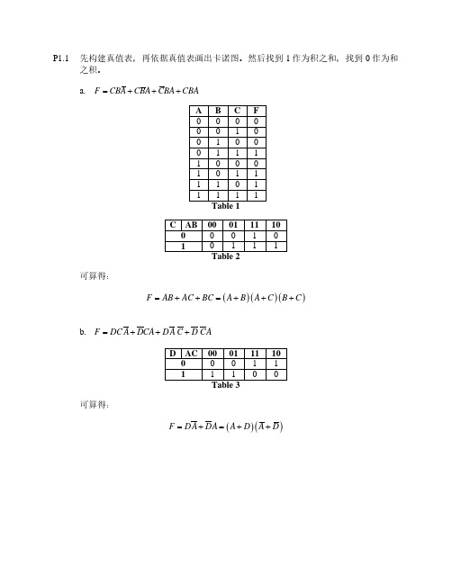
思考题:题3.1.1 组合逻辑电路在结构上不存在输出到输入的 ,因此 状态不影响 状态。
答:反馈回路、输出、输入。
题3.1.2 组合逻辑电路分析是根据给定的逻辑电路图,而确定 。
组合逻辑电路设计是根据给定组合电路的文字描述,设计最简单或者最合理的 。
答:逻辑功能、逻辑电路。
题3.2.1 一组合电路输入信号的变化顺序有以下三种情况,当 时,将可能出现竞争冒险。
(A )00→01→11→10 (B )00→01→10→11 (C )00→10→11→01 答:B题3.2.2 清除竞争冒险的常用方法有(1)电路输出端加 ;(2)输入加 ;(3)增加 。
答:电容,选通脉冲,冗余项。
题3.2.3 门电路的延时时间是产生组合逻辑电路竞争与冒险的唯一原因。
( ) 答:×题3.2.4 根据毛刺产生的方向,组合逻辑的冒险可分为 冒险和 冒险。
答:1型、0型。
题3.2.5 传统的判别方法可采用 和 法来判断组合电路是否存在冒险。
答:代数法、卡诺图。
题3.3.1 进程行为之间执行顺序为 ,进程行为内部执行顺序为 。
答:同时、依次。
题3.3.2 行为描述的基本单元是 ,结构描述的基本单元是 。
答:进程、调用元件语句。
题3.3.3 结构体中的每条VHDL 语句的执行顺序与排列顺序 。
答:无关题3.4.1串行加法器进位信号采用 传递,而并行加法器的进位信号采用 传递。
(A )超前,逐位 (B )逐位,超前 (C )逐位,逐位 (D )超前,超前 答:B题3.4.2 一个有使能端的译码器作数据分配器时,将数据输入端信号连接在 。
答:使能端题 3.4.3 优先编码器输入为70I I -(0I 优先级别最高),输出为2F 、1F 、0F (2F 为高位)。
当使能输入00,651====I I I S 时,输出012F F F 应为 。
答:110题3.4.4 用4位二进制比较器7485实现20位二进制数并行比较,需要 片。
第3章_门电路 课后答案

【题3.4】计算图P3.4电路中的反向器 能驱动多少个同样的反相器。要求 输出的高,低电平符合 。所有的反向器均为74LS系列TTL电路,输入电流 时输出电流的最大值 时输出电流的最大值为 的输出电阻可忽略不计。
【题3.18】在CMOS电路中有时采用图P3.18(a)~(d)所示的扩展功能用法,试分析各图的逻辑功能,写出 的逻辑式。已知电源电压 ,二极管的正向导通压降为0.7V。
【解】
(a)
(b)
(c)
(d)
【题3.19】上题中使用的扩展方法能否用于TTL门电路?试说明理由。
【解】不能用于TTL电路。在图(a)电路中,当C、D、E任何一个为低电平时,分立器件与门的输出将高于TTL与非门的 值,相当于TTL电路的逻辑1状态,分立器件的与门已不能实现与的逻辑功能了。同理,图(d)电路也不能用于TTL电路。
(1)在三极管集电极输出的高、低电压满足 、 的条件下, 的取值范围有多大?
(2)若将OC门改成推拉式输出的TTL门电路,会发生什么问题?
【解】(1)根据三极管饱和导通时的要求可求得RB的最大允许值。三极管的临界饱和基极电流应为
故得到 。
又根据OC门导通时允许的最大负载电流为16mA,可求得Rn的最小允许值。
【题3.13】试分析图P3.13中各电路的逻辑功能,写出输出逻辑函数式。
【解】
(a)
(b)
(c) (OC门)
(d)当
(三态输出的反相器)
高阻态当
数字集成电路分析与设计 第三章答案
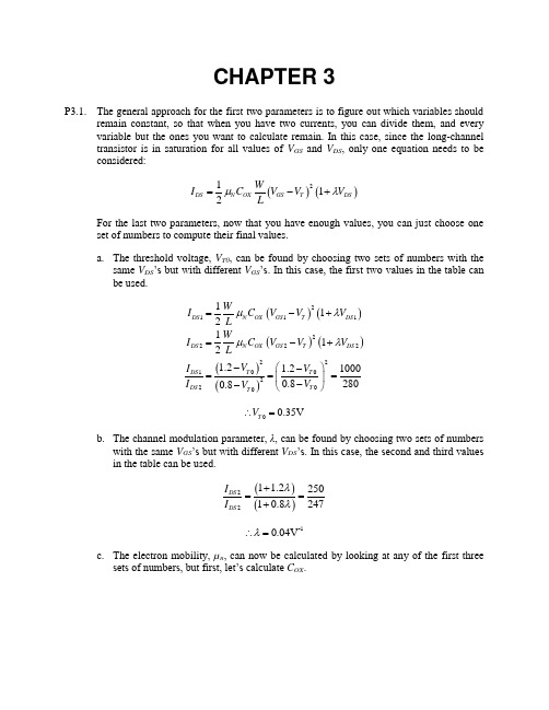
CHAPTER 3P3.1. The general approach for the first two parameters is to figure out which variables shouldremain constant, so that when you have two currents, you can divide them, and every variable but the ones you want to calculate remain. In this case, since the long-channel transistor is in saturation for all values of V GS and V DS , only one equation needs to be considered:()()2112DS N OX GS T DS W I C V V V Lμλ=-+ For the last two parameters, now that you have enough values, you can just choose oneset of numbers to compute their final values.a. The threshold voltage, V T0, can be found by choosing two sets of numbers with the same V DS ’s but with different V GS ’s. In this case, the first two values in the table can be used.()()()()()()211122222201022001121121.2 1.210000.82800.8DS N OX GS T DS DS N OX GS T DS T DS T DS T T W I C V V V L W I C V V V LV I V I V V μλμλ=-+=-+-⎛⎫-===⎪--⎝⎭ 00.35V T V ∴=b. The channel modulation parameter, λ, can be found by choosing two sets of numberswith the same V GS ’s but with different V DS ’s. In this case, the second and third values in the table can be used.()()221 1.225010.8247DS DS I I λλ+==+ -10.04V λ∴=c. The electron mobility, µn , can now be calculated by looking at any of the first three sets of numbers, but first, let’s calculate C OX .631062-31m 10μm22?.210μm1m 10 0.0351 1.610/2.210OX OX t C F cm--=⨯⨯===⨯Now calculate the mobility by using the first set of numbers.()()()()()()()()()()()()22111021262101111 1.21 1.222210002cm 348V-s 1.610(4.75)1.20.3510.04 1.21DS N OX GS T DS N OX T DS N OX GS T DS W W I C V V V C V L LA I W C V V V L μλμλμμλ-=-+=-+===⨯-+-+d. The body effect coefficient gamma, γ, can be calculated by using the last set of numbers since it is the only one that has a V SB greater than 0V.()()()()244124414411221 1.20.468VDS N OX GS T DS DS GS T N OX DS GS T T GS W I C V V V LI V V W C V LV V V V μλμλ=-+-=+-==-==12000.6VT T T T V V V V γγγ=+-====P3.2. The key to this question is to identify the transistor’s region of operation so that gatecapacitance may be assigned appropriately, and the primary capacitor that will dischargedat a rate of V It C ∂∂= by the current source may be identified. Then, because the nodes arechanging, the next region of operation must be identified. This process continues until the transistor reaches steady state behavior. Region 1:Since 0V GS V = the transistor is in the cutoff region. The gate capacitance is allocated to GB C . Since no current will flow through the transistor, all current will come from the source capacitor and the drain node remains unchanged.68-151010V V 6.67100.6671510s nsSB V I I t C C -∆⨯====⨯=∆⨯ The source capacitor will discharge until 1.1V GS T V V == when the transistor enters thesaturation region. This would require that the source node would be at 3.3 1.1 2.2V S G GS V V V =-=-=.()15961510 3.3 2.2 1.6510s 1.65ns 1010C t V I ---⨯∆=∆=-=⨯=⨯ Region 2:The transistor turns on and is in saturation. The current is provided from the capacitor atthe drain node, while the source node remains fairly constant. The capacitance at the drain node is the same as the source node so the rate of change is given by:68-151010V V 6.67100.6671510s nsSB V I I t C C -∆⨯====⨯=∆⨯ Since the transistor is now in the saturation region, GS V can be computed based on thecurrent flowing through the device.()22 1.1 1.37V 3.3 1.37 1.93VGS T GST S G GS kW I V V LV V V V V =-==+==-=-=This is where the source node settles. This means that most of the current is discharged through the transistor until the drain voltage reaches a value that puts the transistor at the edge of saturation.3.3 1.1 2.2VDS GS TD G T V V V V V V =-=-=-=If we assume that all the current comes from the transistor, and the source node remains fixed, the drain node will then discharge at a rate equal to that of the source node in the first region. Region 3:The transistor is now in the linear region the gate capacitance is distributed equally to both GS C and GD C . and both capacitors will discharge at approximately the same rate.-151510V0.28621510510nsV I A t C μ-∆===∆⨯⨯+⨯The graph is shown below.00.511.522.533.5024681012Time (ns)V o l t a g e (V )P3.3. The gate and drain are connected together so that DS GS V V = which will cause thetransistor to remain in saturation. This is a dc measurement so capacitances are not required. Connect the bulk to ground and run SPICE. P3.4. Run SPICE. P3.5. Run SPICE. P3.6. Run SPICE. P3.7. Run SPICE.P3.8. First, let’s look at the various parameters and identify how they affect V T .∙ L – Shorter lengths result in a lower threshold voltage due to DIBL. ∙ W – Narrow width can increase the threshold voltage.∙ V SB – Larger source-bulk voltages (in magnitude) result in a higher threshold voltage. ∙ V DS –Larger drain-source voltages (in magnitude) result in a lower threshold voltage due to DIBL. The transistor with the lowest threshold voltage has the shortest channel, larger width, smallest source-bulk voltage and largest drain-source voltage. This would be the first transistor listed.The transistor with the highest threshold voltage has the longest channel, smallest width,largest source-bulk voltage and smallest drain-source voltage. This would be the last transistor listed. P3.9. Run SPICE.P3.10. Run SPICE. The mobility degradation at high temperatures reduces I on and the increasemobile carriers at high temperatures increase I off . P3.11. The issues that prompted the switch from Al to Cu are resistance and electromigration.Copper wires have lower resistances and are less susceptible to electromigration problems. Copper on the other hand, reacts with the oxygen in SiO 2 and requires cladding around the wires to prevent this reaction.For low-k dielectrics, the target value future technologies is 2.High-k dielectrics are being developed as the gate-insulator material of MOSFET’s. This is because the current insulator material, SiO 2, can not be scaled any longer due to tunneling effects.P3.12. Self-aligned poly gates are fabricated by depositing oxide and poly before the source anddrain regions are implanted. Self-aligned silicides (salicides) are deposited on top of the source and drain regions using the spacers on the sides of the poly gate. P3.13. To compute the length, simply use the wire resistance equation and solve for L .LR TWRTWL ρρ==First convert the units of ρ to terms of μm. Aluminum:2.7μΩρ=cm 6Ω10μΩ⨯610μm100cm ⨯()()()0.027Ωμm1000.812963μm 2.96mm0.027RTWL ρ=====Copper:1.7μΩρ=cm 6Ω10μΩ⨯610μm100cm ⨯()()()0.017Ωμm1000.814706μm 4.71mm0.017RTWL ρ=====P3.14. Generally, the capacitance equation in terms of permittivity constants and spacing is:k C WL tε=a. 4k = ()()()()230048.8510 3.541100SiO k k C WL TL t S S Sεε-====b. 2k = ()()()()30028.8510 1.771100k k C WL TL t S SSεε-====The plots are shown below.Capacitance vs. Spacing01234567800.511.522.533.544.555.5Spacing (um)C a p a c i t a n c e (f F)。
数字集成电路课后习题1-4章作业解析
VOH = VGG − VT = VDD − VT 0 + γ
(
(V
SB
+ 2 φf − 2 φf
))
= VGG − VT 0 − γ VOH + 2 φ f + γ 2 φ f = 1.6 − 0.4 − 0.2 VOH + 0.88 + 0.2 0.88 = 1.388 − 0.2 VOH + 0.88
QOX 6 ×1011 ×1.6 ×10−19 0.06 V = = COX 1.6 ×10⁻⁶ VT0 =−0.99 − (−0.88) − (−0.188) − 0.060 =+0.018 V
计算 PMOS 器件的阈值电压: kT N D 3 ×1017 = φFn = ln 0.026 ln = 0.44 V q ni 1.4 ×10¹⁰
VOL 2 (0.1×10⁻⁴ )(8 ×10⁶ )(1.6 − VOL − 0.4) 2 1 270 1.2 0.4 V − − ( ) OL = 0.1 VOL 2 (1.6 − VOL − 0.4) + 0.6 1 + 0.6
+0.99 V φGC = φFn − φG ( gate ) = 0.44 + 0.55 = QB 0 3 ×10−7 = = +0.188 V QB 0 = 3 ×10⁻⁷ C / cm 2 COX 1.6 ×10−6 QOX 6 ×1011 ×1.6 ×10−19 = = 0.06 V COX 1.6 ×10⁻⁶ VT0 =0.99 − (+0.88) − (+0.188) − 0.060 =−0.138 V
VOH = 1.11V 由此可知,VGG 实际要大于 1.6 V,接近 1.7 V,才能使 VOH 达到 1.2 V。 计算 VOL 时忽略体效应, ∴
数字电子技术基础第三版第三章答案
题3.10数据选择器和数据分配器各具有什么功能?若想将一组并行输入的数据转换成串行输出,应采用哪种电路?
答:数据选择器根据控制信号的不同,在多个输入信号中选择其中一个信号输出。数据分配器则通过控制信号将一个输入信号分配给多个输出信号中的一个。若要将并行信号变成串行信号应采用数据选择器。
试设计符合上述要求的逻辑电路(器件不限)。
解:题目中要求控制信号对不同功能进行选择,故选用数据选择器实现,分析设计要求,得到逻辑表达式:
。
4选1数据选择器的逻辑表达式:
。
对照上述两个表达式,得出数据选择器的连接方式为:
A0=C1,A1=C2, , , , 。
根据数据选择器的连接方程,得到电路如习题3.3图所示。
1
0
0 0
1 0 0 0
1
0
1 0
1 0 0 1
1
1
1 1
1 0 1 0
1
1
0 1
1 0 1 1
1
0
0 0
1 1 0 0
0
0
1 1
1 1 0 1
0
1
1 0
1 1 1 0
0
1
1 0
1 1 1 1
0
0
0 1
(3)由真值表,作函数卡诺图如习题3.1图(b)所示。
卡诺图化简函数,得到最简与或式:
变换F2的表达式
(2)定义逻辑变量0、1信号的含义。无论输入变量、输出变量均有两个状态0、1,这两个状态代表的含义由设计者自己定义。
(3)再根据设计问题的因果关系以及变量定义,列出真值表。
- 1、下载文档前请自行甄别文档内容的完整性,平台不提供额外的编辑、内容补充、找答案等附加服务。
- 2、"仅部分预览"的文档,不可在线预览部分如存在完整性等问题,可反馈申请退款(可完整预览的文档不适用该条件!)。
- 3、如文档侵犯您的权益,请联系客服反馈,我们会尽快为您处理(人工客服工作时间:9:00-18:30)。
VDD = 2.5V R VD Vin=2V M1
W/L = 2.5µ/0.25µ
VS
I = 50µΑ
Figure 0.4 Test configuration for the NMOS device.
9.
a. When R =10kΩ find the operation region, VD and VS. b. When R= 30kΩ again determine the operation region VD, VS c. For the case of R = 10kΩ, would VS increase or decrease if λ ≠ [M, None, 3.3.2] Consider the circuit configuration of Figure 0.5.
VDS (V) -2.5 1 -0.8 -2.5 -2.5 -1.5 -0.8
VSB (V) 0 0 0 0 -1 0 0
ID (µA) -84.375 0.0 -1.04 -56.25 -72.0 -80.625 -66.56
Operation Region?
[M, None, 3.3.2] An NMOS device is plugged into the test configuration shown below in Figure 0.4. The input Vin =2V. The current source draws a constant current of 50 µA. R is a variable resistor that can assume values between 10kΩ and 30 kΩ. Transistor M1 experiences short channel effects and has following transistor parameters: k’ = 110*10-6 V/A2, VT = 0.4 , and VDSAT = 0.6V. The transistor has a W/L = 2.5µ/0.25µ. For simplicity body effect and channel length modulation can be neglected. i.e λ=0, γ=0. .
Rs = 2 kΩ + Vs=3.3V – – VD +
ID
Figure 0.2
Series diode circuit
3.
4.
[E, None, 3.3.2] Figure 0.3 shows NMOS and PMOS devices with drains, source, and gate ports annotated. Determine the mode of operation (saturation, linear, or cutoff) and drain current ID for each of the biasing configurations given below. Verify with SPICE. Use the follow2 –1 ing transistor data: NMOS: k' n = 115µA/V , VT0 = 0.43 V, λ = 0.06 V , PMOS: k' p = 30 2 –1 µA/V , VT0 = –0.4 V, λ = -0.1 V . Assume (W/L) = 1. a. NMOS: VGS = 2.5 V, VDS = 2.5 V. PMOS: VGS = –0.5 V, VDS = –1.25 V. b. NMOS: VGS = 3.3 V, VDS = 2.2 V. PMOS: VGS = –2.5 V, VDS = –1.8 V. c. NMOS: VGS = 0.6 V, VDS = 0.1 V. PMOS: VGS = –2.5 V, VDS = –0.7 V. [E, SPICE, 3.3.2] Using SPICE plot the I-V characteristics for the following devices.
Digital Integrated Circuits - 2nd Ed
3
e. Given the obtained answers, determine for each of the measurements the operation region of the transistor (choose from cutoff, resistive, saturated, and velocity saturated). Annotate your finding in the right-most column of the above.
1
Chapter 3 Problem Set
Chapter 3 PROBLEMS
For all problems, use the device parameters provided in Chapter 3 (Tables 3.2 and 3.5) and the inside back book cover, unless otherwise mentioned. Also assume T = 300 K by default. 1. [E,SPICE,3.2.2] a. Consider the circuit of Figure 0.1. Using the simple model, with VDon = 0.7 V, solve for ID. b. Find ID and VD using the ideal diode equation. Use Is = 10–14 A and T = 300 K. c. Solve for VD1, VD2, and ID using SPICE. d. Repeat parts b and c using IS = 10–16 A, T = 300K, and IS = 10–14A, T = 350 K.
Table 0.2 Measurements taken from the MOS device, at different terminal voltages.
Measurement number 1 2 3 4 5 6 7 8.
VGS (V) -2.5 1 -0.7 -2.0 -2.5 -2.5 -2.5
Measured NMOS transistor data VGS VDS 1.8 1.8 2.5 1.8 1.8 VBS 0 0 0 –1 -2 ID (µA) 1812 1297 1361 1146 1039
Table 0.1
1 2 3 4 5 7.
2.5 2 2 2 2
[E, None, 3.3.2] Given Table 0.2 ,the goal is to derive the important device parameters from these data points. As the measured transistor is processed in a deep-submciron technology, the ‘unified model’ holds. From the material constants, we also could determine that the saturation voltage VDSAT equals -1V. You may also assume that -2ΦF = -0.6V. NOTE: The parameter values on Table 3.3 do NOT hold for this problem. a. Is the measured transistor a PMOS or an NMOS device? Explain your answer. b. Determine the value of VT0. c. Determine γ. d. Determine λ.
0. Explain qualitatively
4
Chapter 3 Problem Set a. Write down the equations (and only those) which are needed to determine the voltage at node X. Do NOT plug in any values yet. Neglect short channel effects and assume that λp = 0. b. Draw the (approximative) load lines for both MOS transistor and resistor. Mark some of the significant points. c. Determine the required width of the transistor (for L = 0.25µm) such that X equals 1.5 V. d. We have, so far, assumed that M1 is a long-channel device. Redraw the load lines assuming that M1 is velocity-saturated. Will the voltage at X rise or fall?
2
Chapter 3 Problem Set
G
D ID S G
S ID D Figure 0.3 NMOS and PMOS devices.
5.
6.
a. NMOS W = 1.2µm, L = 0.25µm b. NMOS W = 4.8µm, L = 0.5µm c. PMOS W = 1.2 µm, L = 0.25 µm d. PMOS W = 4.8 µm, L = 0.5 µm [E, SPICE, 3.3.2] Indicate on the plots from problem 4. a. the regions of operation. b. the effects of channel length modulation. c. Which of the devices are in velocity saturation? Explain how this can be observed on the IV plots. [M, None, 3.3.2] Given the data in Table 0.1 for a short channel NMOS transistor with VDSAT = 0.6 V and k′ =100 µA/V2, calculate VT0, γ, λ, 2|φf|, and W / L: