数字集成电路--电路、系统与设计(第二版)课后练习题 第六章 CMOS组合逻辑门的设计
数字集成电路(中文)第六章
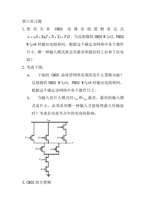
第六章习题1.使用互补CMOS电路实现逻辑表达式X A B C D E F G=++++。
当反相器的NMOS W/L=2, PMOS (()())W/L=6时输出电阻相同,根据这个确定该网络中各个器件尺寸。
哪一种输入模式将会有最差和最好的上拉和下拉电阻?2.考虑下图,a.下面的CMOS晶体管网络实现的是什么逻辑功能?反相器的NMOS W/L=4, PMOS W/L=8时输出电阻相同,根据这个确定该网络中各个器件尺寸。
b.当输入是什么模式时t和p L H t最差。
最初的输入模pH L式是什么,必须采用哪一种输入才能取得最大传输延时?考虑在内部节点中的电容的影响。
3.CMOS组合逻辑a.下图中的两个电路A和B是否实现同一个逻辑函数?如果是的话,是什么逻辑;如果不是的话,给出两个电路的布尔表达式。
b.这两个电路的输出电阻是否总是相同?分析解释。
c.这两个电路的上升下降时间是否总是相同?分析解释。
4. 使用DCVSL实现F ABC ACD=+。
假设A,B,=+和F A BC ACDC,D和他们的反作为输入是允许的。
要求使用最少的晶体管。
5.一个复杂逻辑门电路如下图所示。
a.写出输出F和G的布尔表达式。
并说明这个电路实现的是什么功能。
b.这个电路属于哪一类电路。
6.分析下图所示电路实现什么功能。
7.使用NMOS传输管逻辑实现F ABC ABC ABC ABC=+++。
设计一个DCVSL门实现同样的功能。
假设A,B,C和他们的反都可以实现。
数字集成电路习题答案

W / L 1 根据VGS和VDS确定其处于线性、饱和还是截止状态,并求 I D
的值。
解: (1)nm os:
VGT VGS VT 0 2.5 0.43 2.07 VDS
nm os 处于饱和区 ,Vmin VGT 2.07
2 W V ' I D kn ( )(VGT Vmin min )(1 VDS ) L 2 2 2 . 07 115 (2.072 )(1 0.06 2.5) 2 283.3A
VT0(V)
NMOS PMOS 0.43 -0.4
(V0.5)
0.4 -0.4
VDSAT(V)
0.63 -1
k’(A/V2)
115×10-6 -30×10-6
(V-1)
0.06 -0.1
1.假设设计一个通用0.25m CMOS工艺的反相器,其中PMOS晶体管的 最小尺寸为(W=0.75m,L=0.25m,即W/L=0.75/0.25) , NMOS晶体管 的最小尺寸为(W=0.375m,L=0.25m,即W/L=0.375/0.25) 求出g,VIL,VIH,NML,NMH
( R1 R2 R5 )C5
DCLK 3 R1C1 R1C2 ( R1 R3 )C3 R1C4 R1C5
(b)
DCLK 1 R1C1 ( R1 R2 )C2 R1C3 ( R1 R2 R4 )C4 ( R1 R2 )C5
9 RC
DCLK 2 R1C1 ( R1 R2 )C2 R1C3 ( R1 R2 )C4
( R1 R2 R5 )C5 9 RC
DCLK 3 R1C1 R1C2 ( R1 R3 )C3 R1C4 R1C5
【精品】数字集成电路电路、系统与设计第二版课后练习题第六章CMOS组合逻辑门的设计
【精品】数字集成电路--电路、系统与设计(第二版)课后练习题第六章CMOS组合逻辑门的设计第六章 CMOS组合逻辑门的设计1.为什么CMOS电路逻辑门的输入端和输出端都要连接到电源电压?CMOS电路采用了MOSFET(金属氧化物半导体场效应管)作为开关元件,其中N沟道MOSFET(NMOS)和P沟道MOSFET(PMOS)分别用于实现逻辑门的输入和输出。
NMOS和PMOS都需要连接到电源电压,以使其能够正常工作。
输入端连接到电源电压可以确保信号在逻辑门中正常传递,输出端连接到电源电压可以确保输出信号的正确性和稳定性。
2.为什么在CMOS逻辑门中要使用两个互补的MOSFET?CMOS逻辑门中使用两个互补的MOSFET是为了实现高度抗干扰的逻辑功能。
其中,NMOS和PMOS分别用于实现逻辑门的输入和输出。
NMOS和PMOS的工作原理互补,即当NMOS导通时,PMOS截止,当PMOS导通时,NMOS截止。
这样的设计可以在逻辑门的输出上提供高电平和低电平的稳定性,从而提高逻辑门的抗干扰能力。
3.CMOS逻辑门的输入电压范围是多少?CMOS逻辑门的输入电压范围通常是在0V至电源电压之间,即在低电平和高电平之间。
在CMOS逻辑门中,低电平通常定义为输入电压小于0.3Vdd(电源电压的30%),而高电平通常定义为输入电压大于0.7Vdd(电源电压的70%)。
4.如何设计一个基本的CMOS逻辑门?一个基本的CMOS逻辑门可以由一个NMOS和一个PMOS组成。
其中,NMOS的源极连接到地,栅极连接到逻辑门的输入,漏极连接到PMOS的漏极;PMOS的源极连接到电源电压,栅极连接到逻辑门的输入,漏极连接到输出。
这样的设计可以实现逻辑门的基本功能。
5.如何提高CMOS逻辑门的速度?可以采取以下方法来提高CMOS逻辑门的速度:•减小晶体管的尺寸:缩小晶体管的尺寸可以减小晶体管的电容和电阻,从而提高逻辑门的响应速度。
•优化电源电压:增加电源电压可以提高晶体管的驱动能力,从而加快逻辑门的开关速度。
数字集成电路--电路、系统与设计(第二版)课后练习题第六.
数字集成电路--电路、系统与设计(第⼆版)课后练习题第六.Digital Integrated Circuits - 2nd Ed 11 DESIGN PROJECT Design, lay out, and simulate a CMOS four-input XOR gate in the standard 0.25 micron CMOS process. You can choose any logic circuit style, and you are free to choose how many stages of logic to use: you could use one large logic gate or a combination of smaller logic gates. The supply voltage is set at 2.5 V! Your circuit must drive an external 20 fF load in addition to whatever internal parasitics are present in your circuit. The primary design objective is to minimize the propagation delay of the worst-case transition for your circuit. The secondary objective is to minimize the area of the layout. At the very worst, your design must have a propagation delay of no more than 0.5 ns and occupy an area of no more than 500 square microns, but the faster and smaller your circuit, the better. Be aware that, when using dynamic logic, the precharge time should be made part of the delay. The design will be graded on themagnitude of A × tp2, the product of the area of your design and the square of the delay for the worst-case transition.。
模拟cmos集成电路设计课后题

模拟cmos集成电路设计课后题CMOS(Complementary Metal-Oxide-Semiconductor)集成电路设计是现代电子技术的关键领域之一。
该领域涉及到各种基本电路以及整个系统的设计与优化。
本文将模拟一篇CMOS集成电路设计的课后题,其中包括对基本电路的设计以及系统级优化的考察。
第一部分:基本电路设计(2000字左右)1. 设计一个2输入与门的CMOS电路。
给出电路图,并写出相应的布尔表达式。
2. 为了减小功耗并提高响应速度,经常需要将电路设计为动态逻辑电路。
请设计一个动态逻辑的非门电路,给出电路图,并写出相应的时钟脉冲控制信号。
第二部分:CMOS集成电路设计(2000字左右)3. 设计一个3输入与门的CMOS电路,并对其功耗进行优化。
4. 设计一个4位二进制全加器的CMOS电路,并考虑功耗和面积的优化。
第三部分:系统级优化(2000字左右)5. 将两个2输入与门和一个2输入或门组合成一个3输入与门。
请给出详细的设计流程和最终的电路图。
6. 设计一个8位互补码加法器的CMOS电路,并考虑功耗、面积和延迟的优化。
第一部分:基本电路设计1. 设计一个2输入与门的CMOS电路。
给出电路图,并写出相应的布尔表达式。
CMOS与门的基本电路由PMOS管和NMOS管组成。
在输入A和B分别接入与门电路的两个输入端,而输出则连接到NMOS管和PMOS管接口的并联电路的输出端。
当A和B同时为高电平时,输出才为高电平。
其布尔表达式可以写为:Z = A * B。
2. 为了减小功耗并提高响应速度,经常需要将电路设计为动态逻辑电路。
请设计一个动态逻辑的非门电路,给出电路图,并写出相应的时钟脉冲控制信号。
动态非门电路的设计可以采用PMOS管串联的结构。
当输入S 为高电平时,NMOS管导通,输出结果为0;当输入S为低电平时,PMOS管导通,输出结果为1。
其时钟脉冲控制信号可以表示为:NAND(A, A)。
数字集成电路分析与设计 第六章答案

CHAPTER 6P6.1. The on-resistance of a unit-sized NMOS device.LINEAR | SATURATIONOn-resistance of a unit-sized NMOS device051015202500.20.40.60.811.2V DSR D SThe average on-resistance is approximately 15kΩ. The expression for the average resistance value between DD V and 2DDV .()()()()()()()()222,,22,2223344V DD DSV DS DD DDDD DDV DDDS DD DS D satD satV V V V V I V I I ON DD ON ON DD GS T CN N DDD sat sat ox GS T R V R R V V VE L V I Wv C V V +++===-+==-P6.2. Since the signal must go around the ring twice for one oscillation, the period is :()()()()()()()()()()()()()()331531517301012.51021100.32727.5103100.3173ps TOT PLH PHL P LOAD N LOAD P N W EQP EQN g eff P N P N t N t t N R C R C N R R C W L L N R R C C W W W W --=+=+=+⎛⎫=+++ ⎪⎝⎭⎛⎫=⨯+⨯+ ⎪⎝⎭=⨯⨯=115.77GHz 173TOTf t ps=== Independent of inverter size.P6.3. SPICE.P6.4. The self-capacitance in these cases are the capacitances that will make the transition from0 to DD V or vice versa.a. In this case, all the internal nodes will be charged so the self-capacitance is :()2233313SELF eff eff C C W W W W W C W =++++=b. In this case, all the internal nodes but the one above the bottom NMOS transistor will be charged:()223310SELF eff eff C C W W W W C W =+++=c. If we assume a worst-case scenario, this node will be charged up to DD V from 0.()2233313SELF eff eff C C W W W W W C W =++++=d. The node above the bottom-most NMOS transistor has already been discharged.()223310SELF eff eff C C W W W W C W =+++=P6.5. SPICEP6.6. For optimum sizing given four inverters.()()()()()()()()()()()()44332214111111120012005.8911200203.895.891203.8934.645.89134.64 5.895.8915.8915.8945.890.525.5OUT NPE LE FO SE LE C C SE LE C C SE LE C C SE LE C C SE D LE FO P SE P =⨯=====⨯===⨯===⨯===⨯====⨯+=+=+=∏∑∑For the number of devices for optimum delay:log log log log log log12005.11log log 4N N SE SE PE SE PE N SE PEPE N SE =======Setting 5N =gives:()()()()()()()()5544332215114.1211200290.634.121290.6370.394.12170.3917.054.12117.05 4.124.1214.1214.1244.120.518.5OUT N SE LE C C SE LE C C SE LE C C SE LE C C SE LE C C SE D LE FO P SE P ===⨯===⨯===⨯===⨯===⨯====⨯+=+=+=∑∑P6.7. Solution for NAND3For the first NAND3, LE=5W/3W=5/3. For the second NAND3, the delay is not the same asthe basic inverter. So use the more general formula:310/25/33nand W R LE WR⨯== Same as the first case.a.For equal rise and fall time, we double the sizes of the transistors which leads to:313LE==b.For the pseudo-NMOS, we must first calculate the currents, which are different forpull-up and pull-down in the case of a pseudo-NMOS.For the case of the pull-up, only the PMOS is charging the output, for equal delays,we double the size of the PMOS and NMOS to obtain:23LE=P6.9.a.53 LE=b.53 LE=c.82,33 R FLE LE==d.4,23R FLE LE==P6.10.a.813RLE st gate =b.523FLE nd gate =()()()()()()()()()()()()()()45343433221411451110002222336.8711000145.656.87145.6535.366.8735.36 6.876.871 6.8716.8746.870.51 1.50.5OUT NN N PE LE FO SE LE C C SE LE C C SE LE C C SE LE C C SE D SE P SE P ⎛⎫⎛⎫=⨯== ⎪⎪⎝⎭⎝⎭===⨯===⨯===⨯===⨯====+=+=++++∏∑∑31=P6.12.()()()()()()()()()()()()()()()6345434332211546410001777833311.5510001173.2111.55173.2112511.5525411.5511.55111.551111.55OUT N N PE LE FO BE SE LE C BE C SE LE C BE C SE LE C BE C SE LE C BE C SE D SE P ⎛⎫⎛⎫⎛⎫=⨯⨯== ⎪⎪⎪⎝⎭⎝⎭⎝⎭===⨯⨯===⨯⨯===⨯⨯===⨯⨯====+∏()()41411.550.51 1.5251.2N SE P =+=++++=∑∑()()()()()()()()()()()635735445712(2)(4)800066730333314.6800011095.814.610951175.114.64512(4175.1500)533533OUT PE LE FO BE SE LE C BE C SE LE C BE C SE PE LE FO BE SE ⎛⎫⎛⎫⎛⎫=⨯⨯== ⎪⎪⎪⎝⎭⎝⎭⎝⎭===⨯⨯===⨯⨯===⎛⎫⎛⎫=⨯⨯=⨯+= ⎪⎪⎝⎭⎝⎭==∏∏()()()()()()()()()()()5343322151117.4712001114.317.54114.32317.517.5117.51117.53(17.5)214.60.51 1.5 2.25288.9NN N LE C BE C SE LE C BE C SE LE C BE C SE D SE P SE P =⨯⨯===⎛⎫⎪⨯⨯⎝⎭===⨯⨯====+=+=++++++=∑∑To minimize the delay, a estimate of the number of needed stages can be performed :log log 6637049.610log log 4SE PE N SE =∴===≈ The additional stages can be implemented as inverters attached at the input.P6.14. Consider the following situations :C LV inC LV outOutput high-to-low Output low-to-highIn the first case, the output is making a transition from high to low. The next inverter (not shown) has the PMOS in the cutoff region and the NMOS in the linear region. In these regions, the input capacitance of the next gate can be computed as follows:PMOS: C GP =C g x 2W x (1/2) NMOS: C GN =C g x WFor the output low-to-high transition, we have the PMOS linear and the NMOS cutoff: PMOS: C GP =C g x 2W NMOS: C GN =C g x W (1/2)Clearly, the second case has a larger total capacitance and hence a larger effective C g .P6.15. For this problem we examine ramp inputs as compared to step inputs. In both cases below,the transistors being driven enter the linear region and experience larger gate capacitances than the step input case. Therefore, C g is always larger for ramp inputs.C LC LV outpositive-going input ramp negative-going input rampV V DDP6.16. The FO4 delay for 0.18um is approximately 75ps. For 0.13um it is 55ps. Therefore, theconstant for the equation is roughly 420ps/um.。
数字集成电路(中文)第六章
第六章习题1.使用互补CMOS电路实现逻辑表达式X A B C D E F G=++++。
当反相器的NMOS W/L=2, PMOS (()())W/L=6时输出电阻相同,根据这个确定该网络中各个器件尺寸。
哪一种输入模式将会有最差和最好的上拉和下拉电阻?2.考虑下图,a.下面的CMOS晶体管网络实现的是什么逻辑功能?反相器的NMOS W/L=4, PMOS W/L=8时输出电阻相同,根据这个确定该网络中各个器件尺寸。
b.当输入是什么模式时t和p L H t最差。
最初的输入模pH L式是什么,必须采用哪一种输入才能取得最大传输延时?考虑在内部节点中的电容的影响。
3.CMOS组合逻辑a.下图中的两个电路A和B是否实现同一个逻辑函数?如果是的话,是什么逻辑;如果不是的话,给出两个电路的布尔表达式。
b.这两个电路的输出电阻是否总是相同?分析解释。
c.这两个电路的上升下降时间是否总是相同?分析解释。
4. 使用DCVSL实现F ABC ACD=+。
假设A,B,=+和F A BC ACDC,D和他们的反作为输入是允许的。
要求使用最少的晶体管。
5.一个复杂逻辑门电路如下图所示。
a.写出输出F和G的布尔表达式。
并说明这个电路实现的是什么功能。
b.这个电路属于哪一类电路。
6.分析下图所示电路实现什么功能。
7.使用NMOS传输管逻辑实现F ABC ABC ABC ABC=+++。
设计一个DCVSL门实现同样的功能。
假设A,B,C和他们的反都可以实现。
数字集成电路--电路、系统与设计(第二版)复习资料
第一章 数字集成电路介绍第一个晶体管,Bell 实验室,1947第一个集成电路,Jack Kilby ,德州仪器,1958 摩尔定律:1965年,Gordon Moore 预言单个芯片上晶体管的数目每18到24个月翻一番。
(随时间呈指数增长)抽象层次:器件、电路、门、功能模块和系统 抽象即在每一个设计层次上,一个复杂模块的内部细节可以被抽象化并用一个黑匣子或模型来代替。
这一模型含有用来在下一层次上处理这一模块所需要的所有信息。
固定成本(非重复性费用)与销售量无关;设计所花费的时间和人工;受设计复杂性、设计技术难度以及设计人员产出率的影响;对于小批量产品,起主导作用。
可变成本 (重复性费用)与产品的产量成正比;直接用于制造产品的费用;包括产品所用部件的成本、组装费用以及测试费用。
每个集成电路的成本=每个集成电路的可变成本+固定成本/产量。
可变成本=(芯片成本+芯片测试成本+封装成本)/最终测试的成品率。
一个门对噪声的灵敏度是由噪声容限NM L (低电平噪声容限)和NM H (高电平噪声容限)来度量的。
为使一个数字电路能工作,噪声容限应当大于零,并且越大越好。
NM H = V OH - V IH NM L = V IL - V OL 再生性保证一个受干扰的信号在通过若干逻辑级后逐渐收敛回到额定电平中的一个。
一个门的VTC 应当具有一个增益绝对值大于1的过渡区(即不确定区),该过渡区以两个有效的区域为界,合法区域的增益应当小于1。
理想数字门 特性:在过渡区有无限大的增益;门的阈值位于逻辑摆幅的中点;高电平和低电平噪声容限均等于这一摆幅的一半;输入和输出阻抗分别为无穷大和零。
传播延时、上升和下降时间的定义传播延时tp 定义了它对输入端信号变化的响应有多快。
它表示一个信号通过一个门时所经历的延时,定义为输入和输出波形的50%翻转点之间的时间。
上升和下降时间定义为在波形的10%和90%之间。
对于给定的工艺和门的拓扑结构,功耗和延时的乘积一般为一常数。
数字电路与系统分析第六章习题答案复习进程
数字电路与系统分析第六章习题答案解:1)分析电路结构:该电路是由七个与非门及一个JKFF组成,且CP下降沿触发,属于米勒电路,输入信号X1,X2,输出信号Z。
2)求触发器激励函数:J=X1X2,K=⎺X1⎺X2触发器次态方程:Q n+1=X1X2⎺Q n+⎺X1⎺X2Q n=X1X2⎺Q n+(X1+X2)Q n电路输出方程:Z= ⎺X1⎺X2Q n+X1⎺X2⎺Q n+⎺X1X2⎺Q n+X1X2Q n3)状态转移表:输入X1X2S(t)Q nN(t)Q n+1输出Z0 0 0 0 0 10 11 0 1 0 1 1 1 1 01111111111114)逻辑功能:实现串行二进制加法运算。
X1X2为串行输入的被加数和加数,Q n 为低位来的进位,Q n+1表示向高位的进位。
且电路每来一个CP,实现一次加法运算,Z为本位和,Q在本时钟周期表示向高位的进位,在下一个时钟周期表示从低位来的进位。
例如X1=110110,X2=110100,则运算如下表所示:LSB MSB6.2 试作出101序列检测器的状态图,该同步电路由一根输入线X ,一根输出线Z ,对应与输入序列的101的最后一个“1”,输出Z =1。
其余情况下输出为“0”。
(1) 101序列可以重叠,例如:X :010101101 Z :000101001 (2) 101序列不可以重叠,如:X :010******* Z :0001000010 解:1)S 0:起始状态,或收到101序列后重新检测。
S 1:收到序列“1”。
S 2:连续收到序列“10”。
0/01/0X/Z0/011…100…S 2S 1S 01/00/01/12)0/01/0X/Z0/011…100…S 2S 1S 01/00/01/1解:(1)列隐含表:A B CDC B ×A B CD C B ×AD BC ××(a)(b)进行关联比较得到 所有的等价类为:AD ,BC 。
《数字电子技术(第二版)习题册》答案
《数字电⼦技术(第⼆版)习题册》答案数字电⼦技术(第⼆版)》习题册部分参考答案课题⼀认识数字电路任务⼀认识数制与数制转换⼀、填空题1.时间数值1 02.1 8 153.1 128 2554.75.96.16⼆、选择题1.C 2.B 3.C 4.B 5.C 6.A 7.D三、判断题1.V2. V3. X4.X5.V6.X7.V 8.V 9.X四、问答题1.答:数字电路中的信号为⾼电平或低电平两种状态,它正好与⼆进制的 1 和0 相对应,因此,采⽤⼆进制更加⽅便和实⽤。
2.答:⼗六进制具有数据读写⽅便,与⼆进制相互转换简单,较直观地表⽰位状态等优点。
五、计算题1. (1)7 (2)15 (3)31 (4)2132. (1)[1010]2 (2)[1 0000]23)[100 0000 0000]2 (4)[100 0000 0110]23. (1)[650]8 (4)[3153]84. (1)[010 111]2 (2)[001 101 110]23)[010 000 000]2 (4)[001 110 101 101]25. (1)0FH (2)1FH3)36H (4)0AE63H6. (1)0001 0110 B (2)0010 1010 1110 B3)1011 1000 1111 1100B (4)0011 1111 1101 0101B 任务⼆学习⼆进制数算术运算⼀、填空题1.加减乘除2. 0+0=0 0+1=1 1+0=1 1+1=103.0-0=0 1-0=1 1-1=0 10-1=14.0X0=0 0X1=0 1X0=0 1X1=15.1 06.最⾼正负原码7.字节 8.半字节 9.字⼆、选择题1.C 2.B 3.C 4.B 5.B 6.B 7.C3.x4. V四、问答题1.答:将⼆进制数 001 1移位⾄ 0110,是向左移动⼀位,应做乘2运算。
2.答:将⼆进制数 1010 0000 移位⾄ 0001 0100,是向右移动三位,应做除以 8运算。
- 1、下载文档前请自行甄别文档内容的完整性,平台不提供额外的编辑、内容补充、找答案等附加服务。
- 2、"仅部分预览"的文档,不可在线预览部分如存在完整性等问题,可反馈申请退款(可完整预览的文档不适用该条件!)。
- 3、如文档侵犯您的权益,请联系客服反馈,我们会尽快为您处理(人工客服工作时间:9:00-18:30)。
Chapter 6 Problem Set
Chapter 6 PROBLEMS
1. [E, None, 4.2] Implement the equation X = ((A + B) (C + D + E) + F) G using complementary CMOS. Size the devices so that the output resistance is the same as that of an inverter with an NMOS W/L = 2 and PMOS W/L = 6. Which input pattern(s) would give the worst and best equivalent pull-up or pull-down resistance? Implement the following expression in a full static CMOS logic fashion using no more than 10 transistors: Y = (A ⋅ B) + (A ⋅ C ⋅ E) + (D ⋅ E) + (D ⋅ C ⋅ B) 3. Consider the circuit of Figure 6.1.
2
VDD E 6 A A 6 B 6 C 6 D 6 E F A B C D 4 4 4 4 E 1 A B C D 4 4 4 4 E 1 6 F 6 B 6 C 6 D
Chapter 6 Problem Set
VDD 6
Circuit A
Circuit B
Figure 6.2 Two static CMOS gates.
5.
6.
[E, None, 4.2] The transistors in the circuits of the preceding problem have been sized to give an output resistance of 13 k Ω for the worst-case input pattern. This output resistance can vary, however, if other patterns are applied. a. What input patterns (A–E) give the lowest output resistance when the output is low? What is the value of that resistance? b. What input patterns (A–E) give the lowest output resistance when the output is high? What is the value of that resistance? [E, None, 4.2] What is the logic function of circuits A and B in Figure 6.3? Which one is a dual network and which one is not? Is the nondual network still a valid static logic gate? Explain. List any advantages of one configuration over the other.
VDD B
2.
D
C
A Y
B
A
C
பைடு நூலகம்
D
Figure 6.1 CMOS combinational logic gate.
4.
a. What is the logic function implemented by the CMOS transistor network? Size the NMOS and PMOS devices so that the output resistance is the same as that of an inverter with an NMOS W/L = 4 and PMOS W/L = 8. b. What are the input patterns that give the worst case tpHL and tpLH. State clearly what are the initial input patterns and which input(s) has to make a transition in order to achieve this maximum propagation delay. Consider the effect of the capacitances at the internal nodes. c. Verify part (b) with SPICE. Assume all transistors have minimum gate length (0.25µm). d. If P(A=1)=0.5, P(B=1)=0.2, P(C=1)=0.3 and P(D=1)=1, determine the power dissipation in the logic gate. Assume VDD=2.5V, Cout=30fF and fclk=250MHz. [M, None, 4.2] CMOS Logic a. Do the following two circuits (Figure 6.2) implement the same logic function? If yes, what is that logic function? If no, give Boolean expressions for both circuits. b. Will these two circuits’ output resistances always be equal to each other? c. Will these two circuits’ rise and fall times always be equal to each other? Why or why not?
VDD A B B A B A F B A Circuit A A B B A VDD B A F B A Circuit B Figure 6.3 Two logic functions.
7.
8.
[E, None, 4.2] Compute the following for the pseudo-NMOS inverter shown in Figure 6.4: a. VOL and VOH b. NML and NMH c. The power dissipation: (1) for Vin low, and (2) for Vin high d. For an output load of 1 pF, calculate tpLH, tpHL, and tp. Are the rising and falling delays equal? Why or why not? [M, SPICE, 4.2] Consider the circuit of Figure 6.5.
4
Chapter 6 Problem Set
VDD
F
G
A B
A
A B
A
Figure 6.6 Two-input complex logic gate.
11.
Design and simulate a circuit that generates an optimal differential signal as shown in Figure 6.7. Make sure the rise and fall times are equal.
A Y Y Y Y 50% of VDD A Y Y 0 0 1 1 1 0
Figure 6.7 Differential Buffer.
12.
What is the function of the circuit in Figure 6.8?
VDD (W/L) = 0.6 F A B C D (W/L) = 1.5 Figure 6.5 Pseudo-NMOS gate.
9. 10.
[M, None, 4.2] Implement F = ABC + ACD (and F) in DCVSL. Assume A, B, C, D, and their complements are available as inputs. Use the minimum number of transistors. [E, Layout, 4.2] A complex logic gate is shown in Figure 6.6. a. Write the Boolean equations for outputs F and G. What function does this circuit implement? b. What logic family does this circuit belong to? c. Assuming W/L = 0.5u/0.25u for all nmos transistors and W/L = 2u/0.25u for the pmos transistors, produce a layout of the gate using Magic. Your layout should conform to the following datapath style: (1) Inputs should enter the layout from the left in polysilicon; (2) The outputs should exit the layout at the right in polysilicon (since the outputs would probably be driving transistor gate inputs of the next cell to the right); (3) Power and ground lines should run vertically in metal 1. d. Extract and netlist the layout. Load both outputs (F,G) with a 30fF capacitance and simulate the circuit. Does the gate function properly? If not, explain why and resize the transistors so that it does. Change the sizes (and areas and perimeters) in the HSPICE netlist.