集成电路设计方案习题答案章
数字集成电路分析与设计 第二章答案

CHAPTER 2P2.1. a) The solution for the NMOS case is based on Example 2.4: The equation for V T0 is: 02BT FB F OXQ V V C φ=-- Calculate each individual component.1710()1362OX 077200611196310ln 0.026ln 0.44 V 1.4100.440.550.99 V 4 3.510 F/cm1.610 F/cm 310310/0.188 V 1.610610 1.6100.1.610i FpA GC Fp G gate OXB B OX OX OX n kT q NC Q Q C cmC Q C φφφφεε-------⨯==-=-⨯=-=--=-==⨯=⨯⨯=⨯==⨯⨯⨯⨯==⨯TO 06 V V 0.99(0.88)(0.188)0.0600.018 V=------=+ For the PMOS device:1710()77200611196TO 310ln 0.026ln 0.44 V 1.4100.440.550.99 V 310310/0.188 V1.610610 1.6100.06 V 1.610V 0.99(0.88)(0.188)0.0600.138 D Fn i GC Fn G gate B B OX OX OX N kT q n Q Q C cmC Q C φφφφ-----⨯===⨯=-=+=+⨯=⨯==⨯⨯⨯⨯==⨯=---=-Vb) The magnitude of V T0 would be higher. Since the device is PMOS this means that V T0 islowered. Since the only thing that’s been changed is the doping of the gate, only G φ changes. The new V T0 then becomes:00.110.880.1880.6 1.24V T V =----=-c) Since V T0 will be adjusted with implanted charge (Q I ):60.40.0180.382(1.610)(0.382)IOXIOXI Q C Q V C Q V -=-==⨯To calculate the threshold implant level N I :I I I I qN Q Q N q==For the NMOS device from part(a):6122190.610 3.8210/1.610I I Q N ions cm q --⨯=-=-=⨯⨯ (p-type) For the PMOS device from part(a):612219(1.610)(0.40.138)2.6210/1.610I I Q N ions cm q --⨯-=-=-=⨯⨯ (n-type) For the PMOS device from part(b):612219(1.610)(1.240.4)8.410/1.610I I Q N ions cm q --⨯-=-=-=⨯⨯ (p-type)d) The advantage of having the gate doping be n + for NMOS and p + for PMOS could be seen from analysis above. Doping the gates in such a way leads to devices with lower threshold voltages, but enables the implant adjustment with the same kind of impurities that used in the bulk (p-type for NMOS and n-type for PMOS). If we were to use the same kind of doping in gate as in the body (i.e. n + for PMOS and p + for NMOS) that would lead to higher un-implanted threshold voltages. Adjusting them to the required lower threshold voltage would necessitate implantation of the impurities of the opposite type near the oxide-Si interface. This is not desirable. Also, the doping of the poly gate can be carried out at the same time as the source and drain and therefore does not require an extra step.P2.2. First, convert ox t to units of cm:810100cm222210cm 10ox t -=⨯=ÅÅNow, using the mobility equation:()()20 1.8568130/V70cm0.8114102210pep nGS T ox cm V s V V t μμθ--==≈⎛⎫⎛⎫-+ ⎪⎪+ ⎪⎝⎭⎝⎭P2.3. a) For each transistor, derive the region of operation. In our case, for 0V,0.4V GS V =, thetransistor is in the cutoff region and there is no current. For 0.8V,1.2V GS V =, firstcalculate the saturation voltage Dsat V using:()GS T C DSAT GS T C V V E L V V V E L-=-+For our transistors, this would be:Next, we derive the IV characteristics using the linear and saturation current equations,we get the graphs shown below.IV Characteristic of NMOS01020304050607000.20.40.60.811.2Volts (V)C u r r e n t (u A )IV Characteristic of PMOSVolts (V)C u r r e n t (u A )To plot DS I vs. GS V , first identify the region of operation of the transistor. For GS T V V <, the transistor is in the cutoff region, and there is negligible current. For GS T V V > and GS DS V V ≤, the transistor is in the saturation region and saturation current expression should be used. The graphis shown below. Clearly, it is closer to the linear model.Ids vs. Vgs of NMOS010********607000.20.40.60.811.21.4Vgs (V)I d s (V )P2.4. For each transistor, first determine if the transistor is in cutoff by checking to see if V GS isless than or greater than V T . V T may have to be recalculated if the source of the transistor isn’t grounded. If V GS is less than V T , then it is in cutoff, otherwise, it is in either triode or saturation.To determine if it is in the triode saturation region, check to see if V DS is less than or greater than V DSAT . If V DS is less than V DSAT , then it is in triode, otherwise, it is in saturation. a. Cutoff00.200.2V0.4V GS G S T T GS TV V V V V V V =-=-===∴<b. Cutoff01.2 1.20V0.4V GS G S T T GS TV V V V V V V =-=-===∴<c. Linear01.20 1.2V0.4V GS G S T T GS TV V V V V V V =-=-===∴>The transistor is not in the cutoff region.()()()()()()1.20.460.20.48V 1.20.460.20.2V GS T C DSATGS T C DS DS DSATV V E L V V V E L V V V --===-+-+=∴<d. Saturation: In this case, because D G V V > the transistor is in the saturation region. To see this, recognize that in a long-channel transistor if D G V V >, the transistor is in saturation. Since the saturation drain voltage Dsat V is smaller in a velocity-saturated transistor than in a long-channel transistor, if the long-channel saturation region equation produces a saturated transistor, than the velocity-saturated saturation region equation will also.P2.5. In both cases, the first step it to calculate the maximum value of X V given G V . If thevoltage at the drain is higher than this maximum value, then ,max X X V V =, otherwise,X D V V =. The maximum value of X V is G T V V - but 0T T V V ≠ because of body effect andwe consider its effect.(),max 0001.20.40.988X G T G T G T G T V V V V V V V V V γγγγ=-=-+=--=--+=--=-There are two ways to calculate this, either through iteration or through substitution. Iteration:For the iteration method, we need a starting value for V X,max . A good starting value would be 0 1.20.40.8V G T V V -=-=. We plug this value on the RHS of the equation, calculate a new V X,max and repeat until we reach a satisfactory converged value.Old Vx,max New Vx,max 0.800 0.728 0.728 0.734 0.734 0.734In this, only three iterations are needed to reach 0.734V. Substitution:The term makes things a bit tricky, we get around this by making the following substitution:2,max 2,max 0.880.88X X x V V x =+∴=-Therefore:,max 220.9880.880.98800.2 1.87X V x x x =--=-=+-2,max 1.27, 1.470.880.733,1.28X x V x ===-=-= We use the first value since second value is above V DD . a. Since ,max D X V V >, ,max 0.733V X X V V ==. b. Since ,max D X V V <, ,max 0.6V X X V V ==. P2.6.a. Initially, when 0V in V =, the transistor is in the cutoff region and 0V X V =. Thisvalue is constant until V in exceeds V t 0. From then, X in T V V V =- and body effect must be taken into account. This trend continues until 0.7V X D V V ==, and the value of V inat that point must be calculated. From then on, 0.7V X D V V ==. To plot V X in the second region, we first derive an expression for V X vs. V in.(),max 0000.40.212X G T G T in T in T in in V V V V V V V V V V V γγγγ=-=-+=---=--=--=--Substituting:2,max2,max 0.880.88X X x V V x =+∴=-Therefore:,max 220.2120.880.21200.20.66X in in in V V x V x x V =---=--=+--220.880.88XxV x====-=-⎝⎭Since this is a quadratic function, there will be two graphs of V X. Only one of thesegraphs intersects with V X in the first region. In this case, plug 0.4inV= and see which one gives 0V. In our case, it would be the ‘+’ version of the quadratic.To see where region 3 begins, we simply isolate V in:()()()22220.880.2 2.710.2 2.71440.2 2.711.16V4XinVV=-⎝⎭-+-==+-==The final graph is shown in Figure 错误!未找到引用源。
集成电路版图设计习题答案第二章集成电路制造工艺
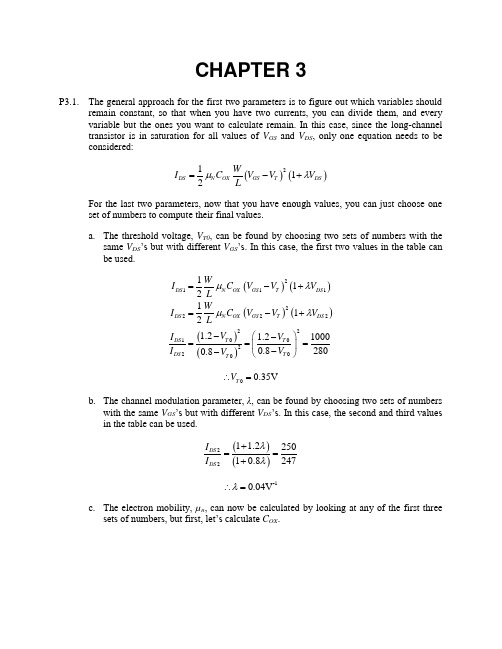
集成电路版图设计习题答案第2章 集成电路制造工艺【习题答案】1.硅片制备主要包括(直拉法)、(磁控直拉法)和(悬浮区熔法)等三种方法。
2.简述外延工艺的用途。
答:外延工艺的应用很多。
外延硅片可以用来制作双极型晶体管,衬底为重掺杂的硅单晶(n +),在衬底上外延十几个微米的低掺杂的外延层(n ),双极型晶体管(NPN )制作在外延层上,其中b 为基极,e 为发射极,c 为集电极。
在外延硅片上制作双极型晶体管具有高的集电结电压,低的集电极串联电阻,性能优良。
使用外延硅片可以解决增大功率和提高频率对集电区电阻要求上的矛盾。
图 外延硅片上的双极型晶体管集成电路制造中,各元件之间必须进行电学隔离。
利用外延技术的PN 结隔离是早期双极型集成电路常采用的电隔离方法。
利用外延硅片制备CMOS 集成电路芯片可以避免闩锁效应,避免硅表面氧化物的淀积,而且硅片表面更光滑,损伤小,芯片成品率高。
外延工艺已经成为超大规模CMOS 集成电路中的标准工艺。
3.简述二氧化硅薄膜在集成电路中的用途。
答:二氧化硅是集成电路工艺中使用最多的介质薄膜,其在集成电路中的应用也非常广泛。
二氧化硅薄膜的作用包括:器件的组成部分、离子注入掩蔽膜、金属互连层之间的绝缘介质、隔离工艺中的绝缘介质、钝化保护膜。
4.为什么氧化工艺通常采用干氧、湿氧相结合的方式?答:干氧氧化就是将干燥纯净的氧气直接通入到高温反应炉内,氧气与硅表面的原子反应生成二氧化硅。
其特点:二氧化硅结构致密、均匀性和重复性好、针孔密度小、掩蔽能力强、与光刻胶粘附良好不易脱胶;生长速率慢、易龟裂不宜生长厚的二氧化硅。
湿氧氧化就是使氧气先通过加热的高纯去离子水(95℃),氧气中携带一定量的水汽,使氧化气氛既含有氧,又含有水汽。
因此湿氧氧化兼有干氧氧化和en +SiO 2n -Si 外延层 n +Si 衬底水汽氧化的作用,氧化速率和二氧化硅质量介于二者之间。
实际热氧化工艺通常采用干、湿氧交替的方式进行。
半导体集成电路+习题答案

第1章 集成电路的基本制造工艺1.6 一般TTL 集成电路与集成运算放大器电路在选择外延层电阻率上有何区别?为什么? 答:集成运算放大器电路的外延层电阻率比一般TTL 集成电路的外延层电阻率高。
第2章 集成电路中的晶体管及其寄生效应复 习 思 考 题2.2 利用截锥体电阻公式,计算TTL “与非”门输出管的CS r ,其图形如图题2.2 所示。
提示:先求截锥体的高度up BL epi m c jc epi T x x T T -----=然后利用公式: b a a b WL T r c -∙=/ln 1ρ , 212∙∙=--BL C E BL S C W L R r ba ab WL Tr c -∙=/ln 3ρ 321C C C CS r r r r ++=注意:在计算W 、L 时, 应考虑横向扩散。
2.3 伴随一个横向PNP 器件产生两个寄生的PNP 晶体管,试问当横向PNP 器件在4种可能的偏置情况下,哪一种偏置会使得寄生晶体管的影响最大?答:当横向PNP 管处于饱和状态时,会使得寄生晶体管的影响最大。
2.8 试设计一个单基极、单发射极和单集电极的输出晶体管,要求其在20mA 的电流负载下 ,OL V ≤0.4V ,请在坐标纸上放大500倍画出其版图。
给出设计条件如下:答: 解题思路⑪由0I 、α求有效发射区周长Eeff L ;⑫由设计条件画图①先画发射区引线孔;②由孔四边各距A D 画出发射区扩散孔;③由A D 先画出基区扩散孔的三边;④由B E D -画出基区引线孔;⑤由A D 画出基区扩散孔的另一边;⑥由A D 先画出外延岛的三边;⑦由C B D -画出集电极接触孔;⑧由A D 画出外延岛的另一边;⑨由I d 画出隔离槽的四周;⑩验证所画晶体管的CS r 是否满足V V O L 4.0≤的条件,若不满足,则要对所作的图进行修正,直至满足V V O L 4.0≤的条件。
(CS C O L r I V V 00ES += 及己知V V C 05.00ES =)第3章 集成电路中的无源元件复 习 思 考 题3.3 设计一个4k Ω的基区扩散电阻及其版图。
集成电路版图设计习题答案第九章集成电路版图设计实例

第9章集成电路版图设计实例【习题答案】1.版图设计关于数字地和模拟地的考虑事项是什么?答:一般的模拟集成电路中,通常既有数字信号又有模拟信号,数字信号和模拟信号之间容易发生干扰。
在版图设计过程中,还要考虑地噪声对电路的影响。
即在整体版图的设计中,需着重考虑电路噪声问题,按照尽量降低噪声的原则进行电路的整体布局。
首先,在总体版图的布局上,尽量将数字部分远离模拟部分,如果总体电路中模拟部分偏多,则在版图设计中将数字部分放在靠边的位置,而且把模拟部分中最容易被数字干扰的部分放到离数字部分最远的位置,同时在数字部分和模拟部分中间用接地的衬底接触来进行隔离,反之亦然。
其次,采用隔离环设计,对每个单元模块都用一层接地的衬底接触,一层接电源的N阱构成的隔离环来进行隔离。
对于整个模拟部分和数字也分别采用相同的隔离环隔离,数字电路的隔离环可以吸收数字电路的衬底噪声,从而可以减少通过衬底串扰到模拟电路的衬底噪声。
隔离环包的层数越多,理论上吸收衬底噪声效果越好。
但是要避免数字电路的p隔离环紧靠模拟电路的p型隔离环,因为在这种情况下数字地的噪声会串扰到模拟地。
从而使模拟地受到干扰。
最后,除了数字模块之外的其它单元模块尽量将距离缩短,这样一方面能尽量地减少互连线经过别的区域引入噪声,同时也能降低引线过长引起电压信号的衰减。
2.总结自己的版图设计技巧和经验。
3. 共质心MOS管设计时的注意事项是什么?答:低精度要求可采用一维共质心,高精度要求必须采用二维共质心。
共质心设计时需保证MO管的对称性和电流通路的对称性。
4. 静电保护的种类以及版图设计注意事项。
答:常用的二极管式的静电保护分为两种方式,一种是用MOS晶体管连接成二极管形式的静电保护,一种利用CMOS工艺中二极管的静电保护。
在MOS型静电保护版图设计中,主要考虑以下几点:●MOS管要分成多个管,叉指结构,以便形成多支路共同放电。
●因为放电瞬间流经MOS管的电流特别大,构成整个放电通路的任何导线的宽度一定要有足够保证,而且CMOS工艺对于每个接触孔能通过的电流密度还有要求,因此还要保证放电通路导线上孔的数目应尽量多。
数字集成电路分析与设计 第三章答案
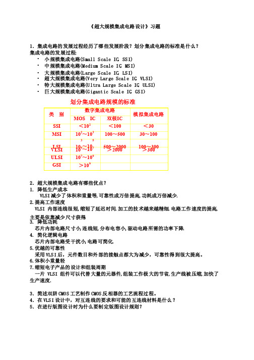
CHAPTER 3P3.1. The general approach for the first two parameters is to figure out which variables shouldremain constant, so that when you have two currents, you can divide them, and every variable but the ones you want to calculate remain. In this case, since the long-channel transistor is in saturation for all values of V GS and V DS , only one equation needs to be considered:()()2112DS N OX GS T DS W I C V V V Lμλ=-+ For the last two parameters, now that you have enough values, you can just choose oneset of numbers to compute their final values.a. The threshold voltage, V T0, can be found by choosing two sets of numbers with the same V DS ’s but with different V GS ’s. In this case, the first two values in the table can be used.()()()()()()211122222201022001121121.2 1.210000.82800.8DS N OX GS T DS DS N OX GS T DS T DS T DS T T W I C V V V L W I C V V V LV I V I V V μλμλ=-+=-+-⎛⎫-===⎪--⎝⎭ 00.35V T V ∴=b. The channel modulation parameter, λ, can be found by choosing two sets of numberswith the same V GS ’s but with different V DS ’s. In this case, the second and third values in the table can be used.()()221 1.225010.8247DS DS I I λλ+==+ -10.04V λ∴=c. The electron mobility, µn , can now be calculated by looking at any of the first three sets of numbers, but first, let’s calculate C OX .631062-31m 10μm22?.210μm1m 10 0.0351 1.610/2.210OX OX t C F cm--=⨯⨯===⨯Now calculate the mobility by using the first set of numbers.()()()()()()()()()()()()22111021262101111 1.21 1.222210002cm 348V-s 1.610(4.75)1.20.3510.04 1.21DS N OX GS T DS N OX T DS N OX GS T DS W W I C V V V C V L LA I W C V V V L μλμλμμλ-=-+=-+===⨯-+-+d. The body effect coefficient gamma, γ, can be calculated by using the last set of numbers since it is the only one that has a V SB greater than 0V.()()()()244124414411221 1.20.468VDS N OX GS T DS DS GS T N OX DS GS T T GS W I C V V V LI V V W C V LV V V V μλμλ=-+-=+-==-==12000.6VT T T T V V V V γγγ=+-====P3.2. The key to this question is to identify the transistor’s region of operation so that gatecapacitance may be assigned appropriately, and the primary capacitor that will dischargedat a rate of V It C ∂∂= by the current source may be identified. Then, because the nodes arechanging, the next region of operation must be identified. This process continues until the transistor reaches steady state behavior. Region 1:Since 0V GS V = the transistor is in the cutoff region. The gate capacitance is allocated to GB C . Since no current will flow through the transistor, all current will come from the source capacitor and the drain node remains unchanged.68-151010V V 6.67100.6671510s nsSB V I I t C C -∆⨯====⨯=∆⨯ The source capacitor will discharge until 1.1V GS T V V == when the transistor enters thesaturation region. This would require that the source node would be at 3.3 1.1 2.2V S G GS V V V =-=-=.()15961510 3.3 2.2 1.6510s 1.65ns 1010C t V I ---⨯∆=∆=-=⨯=⨯ Region 2:The transistor turns on and is in saturation. The current is provided from the capacitor atthe drain node, while the source node remains fairly constant. The capacitance at the drain node is the same as the source node so the rate of change is given by:68-151010V V 6.67100.6671510s nsSB V I I t C C -∆⨯====⨯=∆⨯ Since the transistor is now in the saturation region, GS V can be computed based on thecurrent flowing through the device.()22 1.1 1.37V 3.3 1.37 1.93VGS T GST S G GS kW I V V LV V V V V =-==+==-=-=This is where the source node settles. This means that most of the current is discharged through the transistor until the drain voltage reaches a value that puts the transistor at the edge of saturation.3.3 1.1 2.2VDS GS TD G T V V V V V V =-=-=-=If we assume that all the current comes from the transistor, and the source node remains fixed, the drain node will then discharge at a rate equal to that of the source node in the first region. Region 3:The transistor is now in the linear region the gate capacitance is distributed equally to both GS C and GD C . and both capacitors will discharge at approximately the same rate.-151510V0.28621510510nsV I A t C μ-∆===∆⨯⨯+⨯The graph is shown below.00.511.522.533.5024681012Time (ns)V o l t a g e (V )P3.3. The gate and drain are connected together so that DS GS V V = which will cause thetransistor to remain in saturation. This is a dc measurement so capacitances are not required. Connect the bulk to ground and run SPICE. P3.4. Run SPICE. P3.5. Run SPICE. P3.6. Run SPICE. P3.7. Run SPICE.P3.8. First, let’s look at the various parameters and identify how they affect V T .∙ L – Shorter lengths result in a lower threshold voltage due to DIBL. ∙ W – Narrow width can increase the threshold voltage.∙ V SB – Larger source-bulk voltages (in magnitude) result in a higher threshold voltage. ∙ V DS –Larger drain-source voltages (in magnitude) result in a lower threshold voltage due to DIBL. The transistor with the lowest threshold voltage has the shortest channel, larger width, smallest source-bulk voltage and largest drain-source voltage. This would be the first transistor listed.The transistor with the highest threshold voltage has the longest channel, smallest width,largest source-bulk voltage and smallest drain-source voltage. This would be the last transistor listed. P3.9. Run SPICE.P3.10. Run SPICE. The mobility degradation at high temperatures reduces I on and the increasemobile carriers at high temperatures increase I off . P3.11. The issues that prompted the switch from Al to Cu are resistance and electromigration.Copper wires have lower resistances and are less susceptible to electromigration problems. Copper on the other hand, reacts with the oxygen in SiO 2 and requires cladding around the wires to prevent this reaction.For low-k dielectrics, the target value future technologies is 2.High-k dielectrics are being developed as the gate-insulator material of MOSFET’s. This is because the current insulator material, SiO 2, can not be scaled any longer due to tunneling effects.P3.12. Self-aligned poly gates are fabricated by depositing oxide and poly before the source anddrain regions are implanted. Self-aligned silicides (salicides) are deposited on top of the source and drain regions using the spacers on the sides of the poly gate. P3.13. To compute the length, simply use the wire resistance equation and solve for L .LR TWRTWL ρρ==First convert the units of ρ to terms of μm. Aluminum:2.7μΩρ=cm 6Ω10μΩ⨯610μm100cm ⨯()()()0.027Ωμm1000.812963μm 2.96mm0.027RTWL ρ=====Copper:1.7μΩρ=cm 6Ω10μΩ⨯610μm100cm ⨯()()()0.017Ωμm1000.814706μm 4.71mm0.017RTWL ρ=====P3.14. Generally, the capacitance equation in terms of permittivity constants and spacing is:k C WL tε=a. 4k = ()()()()230048.8510 3.541100SiO k k C WL TL t S S Sεε-====b. 2k = ()()()()30028.8510 1.771100k k C WL TL t S SSεε-====The plots are shown below.Capacitance vs. Spacing01234567800.511.522.533.544.555.5Spacing (um)C a p a c i t a n c e (f F)。
《超大规模集成电路设计》习题(含答案)
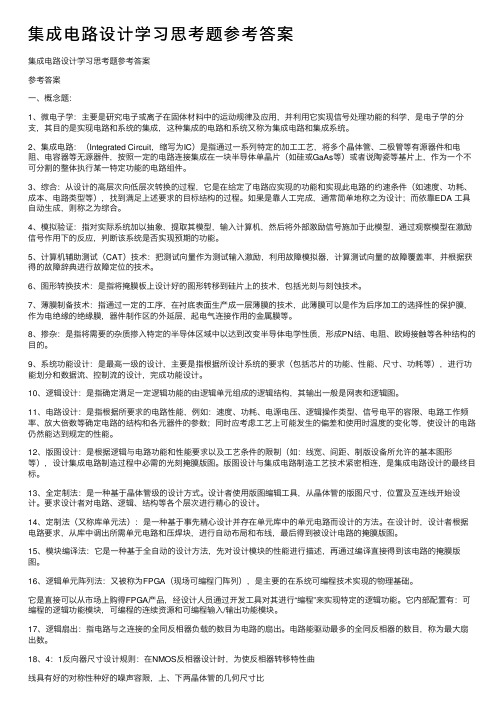
《超大规模集成电路设计》习题1.集成电路的发展过程经历了哪些发展阶段?划分集成电路的标准是什么?集成电路的发展过程:•小规模集成电路(Small Scale IC ,SSI)•中规模集成电路(Medium Scale IC ,MSI)•大规模集成电路(Large Scale IC ,LSI) •超大规模集成电路(Very Large Scale IC ,VLSI)•特大规模集成电路(Ultra Large Scale IC ,ULSI)•巨大规模集成电路(Gigantic Scale IC ,GSI )2.超大规模集成电路有哪些优点?1. 降低生产成本VLSI 减少了体积和重量等,可靠性成万倍提高,功耗成万倍减少.2.提高工作速度VLSI 内部连线很短,缩短了延迟时间.加工的技术越来越精细.电路工作速度的提高,主要是依靠减少尺寸获得. 3. 降低功耗芯片内部电路尺寸小,连线短,分布电容小,驱动电路所需的功率下降.4. 简化逻辑电路芯片内部电路受干扰小,电路可简化.5.优越的可靠性采用VLSI 后,元件数目和外部的接触点都大为减少,可靠性得到很大提高。
6.体积小重量轻7.缩短电子产品的设计和组装周期一片VLSI 组件可以代替大量的元器件,组装工作极大的节省,生产线被压缩,加快了生产速度.3.简述双阱CMOS 工艺制作CMOS 反相器的工艺流程过程。
4.在VLSI 设计中,对互连线的要求和可能的互连线材料是什么?5.在进行版图设计时为什么要制定版图设计规则?划分集成电路规模的标准数字集成电路类别MOS IC 双极IC 模拟集成电路SSI <102<100 <30 MSI 102~103100~500 30~100 LSI 103~105500~2000 100~300 VLSI 105~107>2000 >300 ULSI 107~109GSI >109在芯片尺寸尽可能小的前提下,使得即使存在工艺偏差也可以正确的制造出IC,尽可能地提高电路制备的成品率6.版图验证和检查主要包括哪些方面?u DRC(Design Rule Check):几何设计规则检查;对IC的版图做几何空间检查,保证能在特定的工艺条件下实现所设计的电路,并保证一定的成品率;u ERC(Electrical Rule Check):电学规则检查;检查电源(power)/地(ground)的短路,浮空的器件和浮空的连线等指定的电气特性;u LVS(Loyout versus Schematic):网表一致性检查;将版图提出的网表和原理图的网表进行比较,检查电路连接关系是否正确,MOS晶体管的长/宽尺寸是否匹配,电阻/电容值是否正确等;u LPE(Layout Parameter Extraction):版图寄生参数提取;从版图中提取晶体管的尺寸、结点的寄生电容、连线的寄生电阻等参数,并产生SPICE 格式的网表,用于后仿真验证;u POSTSIM:后仿真,检查版图寄生参数对设计的影响;提取实际版图参数、电阻、电容,生成带寄生量的器件级网表,进行开关级逻辑模拟或电路模拟,以验证设计出的电路功能的正确性和时序性能等,并产生测试向量。
集成电路设计学习思考题参考答案
集成电路设计学习思考题参考答案集成电路设计学习思考题参考答案参考答案⼀、概念题:1、微电⼦学:主要是研究电⼦或离⼦在固体材料中的运动规律及应⽤,并利⽤它实现信号处理功能的科学,是电⼦学的分⽀,其⽬的是实现电路和系统的集成,这种集成的电路和系统⼜称为集成电路和集成系统。
2、集成电路:(Integrated Circuit,缩写为IC)是指通过⼀系列特定的加⼯⼯艺,将多个晶体管、⼆极管等有源器件和电阻、电容器等⽆源器件,按照⼀定的电路连接集成在⼀块半导体单晶⽚(如硅或GaAs等)或者说陶瓷等基⽚上,作为⼀个不可分割的整体执⾏某⼀特定功能的电路组件。
3、综合:从设计的⾼层次向低层次转换的过程,它是在给定了电路应实现的功能和实现此电路的约速条件(如速度、功耗、成本、电路类型等),找到满⾜上述要求的⽬标结构的过程。
如果是靠⼈⼯完成,通常简单地称之为设计;⽽依靠EDA ⼯具⾃动⽣成,则称之为综合。
4、模拟验证:指对实际系统加以抽象,提取其模型,输⼊计算机,然后将外部激励信号施加于此模型,通过观察模型在激励信号作⽤下的反应,判断该系统是否实现预期的功能。
5、计算机辅助测试(CAT)技术:把测试向量作为测试输⼊激励,利⽤故障模拟器,计算测试向量的故障覆盖率,并根据获得的故障辞典进⾏故障定位的技术。
6、图形转换技术:是指将掩膜板上设计好的图形转移到硅⽚上的技术,包括光刻与刻蚀技术。
7、薄膜制备技术:指通过⼀定的⼯序,在衬底表⾯⽣产成⼀层薄膜的技术,此薄膜可以是作为后序加⼯的选择性的保护膜,作为电绝缘的绝缘膜,器件制作区的外延层,起电⽓连接作⽤的⾦属膜等。
8、掺杂:是指将需要的杂质掺⼊特定的半导体区域中以达到改变半导体电学性质,形成PN结、电阻、欧姆接触等各种结构的⽬的。
9、系统功能设计:是最⾼⼀级的设计,主要是指根据所设计系统的要求(包括芯⽚的功能、性能、尺⼨、功耗等),进⾏功能划分和数据流、控制流的设计,完成功能设计。
(整理)集成电路设计习题答案1-5章
CH11.按规模划分,集成电路的发展已经经历了哪几代?它的发展遵循了一条业界著名的定律,请说出是什么定律?晶体管-分立元件-SSI-MSI-LSI-VLSI-ULSI-GSI-SOC。
MOORE定律2.什么是无生产线集成电路设计?列出无生产线集成电路设计的特点和环境。
拥有设计人才和技术,但不拥有生产线。
特点:电路设计,工艺制造,封装分立运行。
环境:IC产业生产能力剩余,人们需要更多的功能芯片设计3.多项目晶圆(MPW)技术的特点是什么?对发展集成电路设计有什么意义?MPW:把几到几十种工艺上兼容的芯片拼装到一个宏芯片上,然后以步行的方式排列到一到多个晶圆上。
意义:降低成本。
4.集成电路设计需要哪四个方面的知识?系统,电路,工具,工艺方面的知识CH21.为什么硅材料在集成电路技术中起着举足轻重的作用 ?原材料来源丰富,技术成熟,硅基产品价格低廉2.GaAs和InP材料各有哪些特点? P10,11 3.怎样的条件下金属与半导体形成欧姆接触?怎样的条件下金属与半导体形成肖特基接触?接触区半导体重掺杂可实现欧姆接触,金属与掺杂半导体接触形成肖特基接触4.说出多晶硅在CMOS工艺中的作用。
P13 5.列出你知道的异质半导体材料系统。
GaAs/AlGaAs, InP/ InGaAs, Si/SiGe, 6.SOI材料是怎样形成的,有什么特点?SOI绝缘体上硅,可以通过氧隔离或者晶片粘结技术完成。
特点:电极与衬底之间寄生电容大大减少,器件速度更快,功率更低7. 肖特基接触和欧姆型接触各有什么特点?肖特基接触:阻挡层具有类似PN结的伏安特性。
欧姆型接触:载流子可以容易地利用量子遂穿效应相应自由传输。
8. 简述双极型晶体管和MOS晶体管的工作原理。
P19,21CH31.写出晶体外延的意义,列出三种外延生长方法,并比较各自的优缺点。
意义:用同质材料形成具有不同掺杂种类及浓度而具有不同性能的晶体层。
外延方法:液态生长,气相外延生长,金属有机物气相外延生长2.写出掩膜在IC制造过程中的作用,比较整版掩膜和单片掩膜的区别,列举三种掩膜的制造方法。
- 1、下载文档前请自行甄别文档内容的完整性,平台不提供额外的编辑、内容补充、找答案等附加服务。
- 2、"仅部分预览"的文档,不可在线预览部分如存在完整性等问题,可反馈申请退款(可完整预览的文档不适用该条件!)。
- 3、如文档侵犯您的权益,请联系客服反馈,我们会尽快为您处理(人工客服工作时间:9:00-18:30)。
集成电路设计方案习题答案章
CH1
1.按规模划分,集成电路的发展已经经历了哪几代?它的发展遵循了一条业界著名的定律,请说出是什么定律?
晶体管-分立元件-SSI-MSI-LSI-VLSI-ULSI-GSI-SOC。
MOORE 定律
2.什么是无生产线集成电路设计?列出无生产线集成电路设计的特点和环境。
拥有设计人才和技术,但不拥有生产线。
特点:电路设计,工艺制造,封装分立运行。
环境:IC产业生产能力剩余,人们需要更多的功能芯片设计
3.多工程晶圆<MPW)技术的特点是什么?对发展集成电路设计有什么意义?
MPW:把几到几十种工艺上兼容的芯片拼装到一个宏芯片上,然后以步行的方式排列到一到多个晶圆上。
意义:降低成本。
4.集成电路设计需要哪四个方面的知识?
系统,电路,工具,工艺方面的知识
CH2
1.为什么硅材料在集成电路技术中起着举足轻重的作用?
原材料来源丰富,技术成熟,硅基产品价格低廉2.GaAs和InP材料各有哪些特点? P10,11
3.怎样的条件下金属与半导体形成欧姆接触?怎样的条件下金属与半导体形成肖特基接触?
接触区半导体重掺杂可实现欧姆接触,金属与掺杂半导体接触形成肖特基接触
4.说出多晶硅在CMOS工艺中
的作用。
P13
5.列出你知道的异质半导体材料系统。
GaAs/AlGaAs, InP/ InGaAs, Si/SiGe,
6.SOI材料是怎样形成的,有什么特点?
SOI绝缘体上硅,能够经过氧隔离或者晶片粘结技术完成。
特点:电极与衬底之间寄生电容大大减少,器件速度更快,功率更低
7. 肖特基接触和欧姆型接触各有什么特点?
肖特基接触:阻挡层具有类似PN结的伏安特性。
欧姆型接触:载流子能够容易地利用量子遂穿效应相应自由传输。
8. 简述双极型晶体管和MOS晶体管的工作原理。
P19,21
CH31.写出晶体外延的意义,列出三种外延生长方法,并比较各自的优缺点。
意义:用同质材料形成具有不同掺杂种类及浓度而具有不同性能的晶体层。
外延方法:液态生长,气相外延生长,金属有机物气相外延生长
2.写出掩膜在IC制造过程中的作用,比较整版掩膜和单片掩膜的区别,列举三种掩膜的制造方法。
P28,29
3.写出光刻的作用,光刻有哪两种曝光方式?作用:把掩膜上的图形转换成晶圆上的器件结构。
曝光方式有接触与非接触两种。
4.X射线制版和直接电子束直写技术替代光刻技术有什么优缺点?
X 射线<X-ray)具有比可见
光短得多的波长,可用来制作更高分辨率的掩膜版。
电子束扫描法,,由于高速电子的波长很短,分辨率很高
5.说出半导体工艺中掺杂的作用,举出两种掺杂方法,并比较其优缺点。
热扩散掺杂和离子注入法。
与热扩散相比,离子注入法的优点如下:1.掺杂的过程可经过调整杂质剂量与能量来精确控制杂质分布。
2.可进行小剂量的掺杂。
3.可进行极小深度的掺杂。
4.较低的工业温度,故光刻胶可用作掩膜。
5.可供掺杂的离子种类较多,离子注入法也可用于制作隔离岛。
缺点:价格昂贵,大剂量注入时,半导体晶格会遭到严重破坏且难以恢复
6.列出干法和湿法氧化法形成SiO2的化学反应式。
干氧湿氧
CH4
1.Si工艺和GaAs工艺都有哪些晶体管结构和电路形式?见表4.1
2.比较CMOS工艺和GaAs工艺的特点。
CMOS工艺技术成熟,功耗低。
GaAs工艺技术不成熟,工作频率高。
3.什么是MOS工艺的特征尺
寸?
工艺能够实现的平面结构的最小宽度,一般指最小栅长。
4.为什么硅栅工艺取代铝栅工
艺成为CMOS工艺的主流技术?
铝栅工艺缺点是,制造源漏极与制造栅极需要两次掩膜步骤<MASK STEP),不容易
对齐。
硅栅工艺的优点是:自对准的,它无需重叠设计,减小了电容,提高了速度,增加了电路的稳定性。
5.为什么在栅长相同的情况下
NMOS管速度要高于PMOS 管?
因为电子的迁移率大于空穴的迁移率
6.简述CMOS工艺的基本工艺流程。
P.52
7.常规N-Well CMOS工艺需要哪几层掩膜?每层掩膜分别有什么作用?P50表4.3
CH5
6.说出MOSFET的基本结构。
MOSFET由两个PN结和一个MOS电容组成。
7.写出MOSFET的基本电流方
程。
8.MOSFET的饱和电流取决于
哪些参数?
饱和电流取决于栅极宽度W,栅极长度L,栅-源之间压降,阈值电压,氧化层厚度,氧化层介电常数
9.为什么说MOSFET是平方率
器件?
因为MOSFET的饱和电流具有平方特性
10.什么是MOSFET的阈值电
压?它受哪些因素影响?
阈值电压就是将栅极下面的Si表面从P型Si变成N型Si 所必要的电压。
影响它的因素有4个:材料的功函数之差,SiO2层中能够移动的正离子的影响,氧化层中固定电荷的影响,界面势阱的影响
11.什么是MOS器件的体效
应?。