
BU406;中文规格书,Datasheet资料
BU406
SILICON NPN SWITCHING TRANSISTOR
s
STMicroelectronics PREFERRED SALESTYPE
s NPN TRANSISTOR
s
VERY HIGH SWITCHING SPEED
APPLICATIONS:
s HORIZONTAL DEFLECTION FOR MONOCHROME TV DESCRIPTION The BU406 is a silicon Epitaxial Planar NPN transistor in Jedec TO-220 plastic package.
It is a fast switching device for use in horizontal deflection output stages of large screens MTV receivers with 110o CRT.
®
February 2003 ABSOLUTE MAXIMUM RATINGS
1/4
e P r o d u c t (s ) - O b s o l e t e P r o d u c t (s ) -
O
b s o l e t e P r o d u
c t (s ) - O b s o l e t e P
THERMAL DATA
ELECTRICAL CHARACTERISTICS (T case = 25 o C unless otherwise specified)
BU406
O b s o l e t e P r o d u c t (s ) - O b
BU406
O
b s o l e t e P r o d u
c t (s ) - O b s o l e t e P r o
d u c t (s ) Information furnished is believed to b
e accurate and reliable. However, STMicroelectronics assumes no responsibility for the consequences o
f use of such information nor for any infringement of patents or other rights of third parties which may result from its use. No license is granted by implication or otherwise under any patent or patent rights of STMicroelectronics. Specification mentioned in this publication are subject to change without notice. This publication supersedes and replaces all information previously supplied. STMicroelectronics products are not authorized for use as critical components in life support devices or systems without express written approval of STMicroelectronics.
The ST logo is a trademark of STMicroelectronics
© 2003 STMicroelectronics – Printed in Italy – All Rights Reserved
STMicroelectronics GROUP OF COMPANIES
Australia - Brazil - Canada - China - Finland - France - Germany - Hong Kong - India - Israel - Italy - Japan - Malaysia - Malta - Morocco - Singapore - Spain - Sweden - Switzerland - United Kingdom - United States.
BU406
O b s o l e t e P r o d u c t (s ) - O b s o l e t e P r o d u c t (s )
分销商库存信息: STM
BU406。
B0540WS-7;中文规格书,Datasheet资料
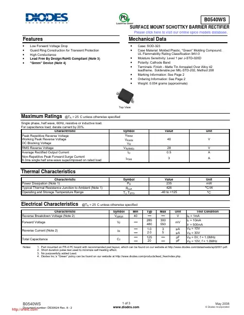
SURFACE MOUNT SCHOTTKY BARRIER RECTIFIERFeatures• Low Forward Voltage Drop• Guard Ring Construction for Transient Protection • High Conductance• Lead Free By Design/RoHS Compliant (Note 3) • "Green" Device (Note 4)Mechanical Data• Case: SOD-323• Case Material: Molded Plastic, "Green" Molding Compound.UL Flammability Rating Classification 94V-0• Moisture Sensitivity: Level 1 per J-STD-020D• Polarity: Cathode Band• Terminals: Finish - Matte Tin Annealed Over Alloy 42leadframe. Solderable per MIL-STD-202, Method 208 • Marking Information: See Page 2• Ordering Information: See Page 2• Weight: 0.004 grams (approximate)Top ViewMaximum Ratings@T A = 25°C unless otherwise specifiedSingle phase, half wave, 60Hz, resistive or inductive load.For capacitance load, derate current by 20%.Characteristic Symbol Value UnitPeak Repetitive Reverse Voltage Working Peak Reverse Voltage DC Blocking Voltage V RRMV RWMV R40 VRMS Reverse Voltage V R(RMS)28 V Average Rectified Output Current I O0.5 ANon-Repetitive Peak Forward Surge Current8.3ms single half sine-wave superimposed on rated load I FSM3 A Thermal CharacteristicsCharacteristic Symbol Value Unit Power Dissipation (Note 1) P D235 mW Typical Thermal Resistance Junction to Ambient (Note 1) RθJA426 °C/W Operating and Storage Temperature Range T J, T STG-40 to +125 °CElectrical Characteristics@T A = 25°C unless otherwise specifiedCharacteristic Symbol Min Typ Max Unit Test Condition Reverse Breakdown Voltage (Note 2) V(BR)R40 ⎯⎯V I R = 1mAForward Voltage V F⎯285480300550mVI F = 10mAI F = 500mAReverse Current (Note 2) I R ⎯⎯1.02.035μAμAV R = 10VV R = 30VTotal Capacitance C T ⎯⎯12520⎯⎯pFpFV R = 0V, f = 1.0MHzV R = 10V, f = 1.0MHzNotes: 1. Part mounted on FR-4 PC board with recommended pad layout, which can be found on our website at /datasheets/ap02001.pdf.2. Short duration pulse test used to minimize self-heating effect.3. No purposefully added Lead.4. Diodes Inc.'s "Green" policy can be found on our website at /products/lead_free/index.php.Please click here to visit our online spice models database.10100V, INSTANTANEOUS REVERSE VOLTAGE (V)Fig. 2 Typical Reverse CharacteristicsRI,INSTANTANEOUSFORWARDCURRENT(mA)FV, INSTANTANEOUS FORWARD VOLTAGE (V)Fig. 1 Typical Forward CharacteristicsF100C,TOTALCAPACITANCE(pF)TV, DC REVERSE VOLTAGE (V)Fig. 3 Total Capacitance vs. Reverse VoltageR0.250.50050100I,AVE150RAGEFORWARDCURRENT(A)F(AV)T, TERMINAL TEMPERATURE (C)Fig. 4 Forward Current Derating CurveT°0.751.02575125Ordering Information(Note 5)Part Number Case PackagingB0540WS-7 SOD-323 3000/Tape & ReelNotes: 5. For packaging details, go to our website at /datasheets/ap02007.pdf.Marking InformationSF SF = Product Type Marking CodePackage Outline DimensionsSuggested Pad LayoutIMPORTANT NOTICEDiodes Incorporated and its subsidiaries reserve the right to make modifications, enhancements, improvements, corrections or other changes without further notice to any product herein. Diodes Incorporated does not assume any liability arising out of the application or use of any product described herein; neither does it convey any license under its patent rights, nor the rights of others. The user of products in such applications shall assume all risks of such use and will agree to hold Diodes Incorporated and all the companies whose products are represented on our website, harmless against all damages.LIFE SUPPORTDiodes Incorporated products are not authorized for use as critical components in life support devices or systems without the expressed written approval of the President of Diodes Incorporated.SOD-323 Dim Min Max A 0.25 0.35 B 1.20 1.40 C 2.30 2.70 H 1.60 1.80 J 0.00 0.10 K 1.0 1.1 L0.20 0.40 M 0.10 0.15α0° 8°All Dimensions in mmDimensions Value (in mm)Z 3.75 G 1.05 X 0.65 Y 1.35 C 2.40分销商库存信息: DIODESB0540WS-7。
BU4066BC中文资料

14 VDD 13 C1 12 C4 11 I / O4 10 O / I4 9 O / I3 8 I / O3
DIP / SOP / SSOP
IN / OUT
VDD
VDD VDD
OUT / IN
CONT VSS
1
元器件交易网
Standard ICs
BU4066BC / BU4066BCF / BU4066BCFV
—
pF
— f = 1MHz
—
Input capacitance (switch input) CS
—
10
—
pF
— f = 1MHz
—
2
元器件交易网
Standard ICs
BU4066BC / BU4066BCF / BU4066BCFV
•Electrical characteristics
Unit
VDD
– 0.5 ~ + 20
V
Pd
1000 (DIP) , 450 (SOP) 350 (SSOP)
mW
Topr
– 40 ~ + 85
°C
Tstg
– 55 ~ + 150
°C
VIN
– 0.5 ~ VDD + 0.5
V
•Electrical characteristics
DC characteristics (unless otherwise noted, Ta = 25°C, VSS = 0V)
Fig. 3 Power dissipation vs. ambient temperature
•External dimensions (Units: mm)
4066B中文资料

Fig.3 Schematic diagram (one switch).
January 1995
2
元器件交易网
Philips Semiconductors
Product specification
Quadruple bilateral switches
RATINGS Limiting values in accordance with the Absolute Maximum System (IEC 134) Power dissipation per switch For other RATINGS see Family Specifications DC CHARACTERISTICS Tamb = 25 °C VDD V 5 ON resistance 10 15 5 ON resistance 10 15 5 ON resistance ‘∆’ ON resistance between any two channels OFF state leakage current, any channel OFF En input voltage LOW 10 15 5 10 15 5 10 15 5 10 15 VIL IOZ ∆RON RON RON RON SYMBOL MIN. − − − − − − − − − − − − − − − − − − − − − 2,25 4,50 6,75 TYP. MAX. 350 80 60 115 50 40 120 65 50 25 10 5 2500 Ω 245 Ω 175 Ω 340 Ω 160 Ω 115 Ω 365 Ω 200 Ω 155 Ω − − − − − Ω Ω Ω nA nA 1 V 2 V 2 V En at VSS P max.
BU406TU;BU406;BU408;中文规格书,Datasheet资料

(3.00) (3.70) 15.90 ±0.20 18.95MAX.
9.20 ±0.20 (1.46)
10.08 ±0.30
13.08 ±0.20 (1.00)
1.27 ±0.10
2.54TYP [2.54 ±0.20]
1.52 ±0.10
0.80 ±0.10 2.54TYP [2.54 ±0.20]
0.50
+0.10 –0.05
2.40 ±0.20
10.00 ±0.20
© 2012 Fairchild Semiconductor Corporation
BU406/406H/408 Rev. B0
3
/
Dimensions in Millimeters
Min. 10
Max.
5 100
1
1
Units
mA μA mA
mA
1
V
1
V
1
V
1.2
V
1.2
V
1.5
V
MHz
0.75
μs
0.4
μs
0.4
μs
© 2012 Fairchild Semiconductor Corporation
BU406/406H/408 Rev. B0
1
/
TRADEMARKS
The following includes registered and unregistered trademarks and service marks, owned by Fairchild Semiconductor and/or its global subsidiaries, and is not intended to be an exhaustive list of all such trademarks.
BU406-S中文资料

●7 A Continuous Collector Current ●15 A Peak Collector Current ●60 W at 25°C Case Temperatureabsolute maximum ratings at 25°C case temperature (unless otherwise noted)NOTE1:This value applies for t p ≤ 10 ms, duty cycle ≤ 2%.RATINGSYMBOL VALUE UNIT Collector-base voltage (I E = 0)BU406BU407V CBO 400330V Collector-emitter voltage (V BE = -2 V)BU406BU407V CEX 400330V Collector-emitter voltage (I B = 0)BU406BU407V CEO 200150V Emitter-base voltage V EB 6V Continuous collector current I C 7A Peak collector current (see Note 1)I CM 15A Continuous base currentI B 4A Continuous device dissipation at (or below) 25°C case temperature P tot 60WOperating junction temperature range T j -55 to +150°C Storage temperature range T stg-55 to +150°CNOTES:2.These parameters must be measured using pulse techniques, t p = 300 µs, duty cycle ≤ 2%.3.These parameters must be measured using voltage-sensing contacts, separate from the current carrying contacts.4.T o obtain f t the [h FE ] response is extrapolated at the rate of -6 dB per octave from f = 1 MHz to the frequency at which [h FE ] = 1.† Voltage and current values shown are nominal; exact values vary slightly with transistor parameters.electrical characteristics at 25°C case temperature (unless otherwise noted)P ARAMETERTEST CONDITIONSMIN TYPMAXUNIT V (BR)CEOCollector-emitter breakdown voltageI C = 30 mA I B =0140VI CESCollector-emitter cut-off currentV CE = 400 V V CE = 330 VV CE = 250 V V CE = 200 V V CE = 250 V V CE = 200V V BE =0V BE =0V BE =0V BE =0V BE =0V BE =0T C = 150°C T C = 150°CBU406BU407BU406BU407BU406BU407550.10.111mAI EBO Emitter cut-off current V EB = 6 V I C =01mA h FE Forward current transfer ratio V CE = 10 V V CE = 10 V I C =4A I C =0.5A (see Notes 2 and 3)1220V CE(sat)Collector-emitter saturation voltage I B = 0.5 A I C = 5A (see Notes 2 and 3)1V V BE(sat)Base-emitter saturation voltage I B = 0.5 A I C = 5A (see Notes 2 and 3) 1.2V f t Current gain bandwidth product V CE = 5 V I C = 0.5A f = 1 MHz (see Note 4)6MHz C obOutput capacitanceV CB = 20 VI E =0f = 1 MHz60pFthermal characteristicsP ARAMETERMINTYPMAX UNIT R θJC Junction to case thermal resistance 2.08°C/W R θJAJunction to free air thermal resistance70°C/Winductive-load-switching characteristics at 25°C case temperature (unless otherwise noted)P ARAMETER TEST CONDITIONS †MINTYP MAXUNIT t s Storage time I C = 5 AI B(end) = 0.5A(see Figures 1 and 2)2.7µs t (off)T urn off time750nsPARAMETER MEASUREMENT INFORMATION。
CD4063BM96E4,CD4063BM96G4,CD4063BNSRE4,CD4063BNSRG4,CD4063BM, 规格书,Datasheet 资料

Data sheet acquired from Harris SemiconductorSCHS050C − Revised October 2003The CD4063B types are supplied in 16-leadhermetic dual-in-line ceramic packages(F3A suffix), 16-lead dual-in-line plasticpackages (E suffix), 16-lead small-outlinepackages (M, M96, MT, and NSR suffixes), and16-lead thin shrink small-outline packages(PW and PWR suffixes). This device ispin-compatible with the standard 7485 TTL type.Copyright © 2003, Texas Instruments IncorporatedPACKAGING INFORMATIONOrderable Device Status(1)PackageType PackageDrawingPins PackageQtyEco Plan(2)Lead/Ball Finish MSL Peak Temp(3)CD4063BE ACTIVE PDIP N1625Pb-Free(RoHS)CU NIPDAU N/A for Pkg TypeCD4063BEE4ACTIVE PDIP N1625Pb-Free(RoHS)CU NIPDAU N/A for Pkg Type CD4063BF ACTIVE CDIP J161TBD A42N/A for Pkg Type CD4063BF3A ACTIVE CDIP J161TBD A42N/A for Pkg Type CD4063BM ACTIVE SOIC D1640Green(RoHS&no Sb/Br)CU NIPDAU Level-1-260C-UNLIMCD4063BM96ACTIVE SOIC D162500Green(RoHS&no Sb/Br)CU NIPDAU Level-1-260C-UNLIMCD4063BM96E4ACTIVE SOIC D162500Green(RoHS&no Sb/Br)CU NIPDAU Level-1-260C-UNLIMCD4063BM96G4ACTIVE SOIC D162500Green(RoHS&no Sb/Br)CU NIPDAU Level-1-260C-UNLIMCD4063BME4ACTIVE SOIC D1640Green(RoHS&no Sb/Br)CU NIPDAU Level-1-260C-UNLIMCD4063BMG4ACTIVE SOIC D1640Green(RoHS&no Sb/Br)CU NIPDAU Level-1-260C-UNLIMCD4063BMT ACTIVE SOIC D16250Green(RoHS&no Sb/Br)CU NIPDAU Level-1-260C-UNLIMCD4063BMTE4ACTIVE SOIC D16250Green(RoHS&no Sb/Br)CU NIPDAU Level-1-260C-UNLIMCD4063BMTG4ACTIVE SOIC D16250Green(RoHS&no Sb/Br)CU NIPDAU Level-1-260C-UNLIMCD4063BNSR ACTIVE SO NS162000Green(RoHS&no Sb/Br)CU NIPDAU Level-1-260C-UNLIMCD4063BNSRE4ACTIVE SO NS162000Green(RoHS&no Sb/Br)CU NIPDAU Level-1-260C-UNLIMCD4063BNSRG4ACTIVE SO NS162000Green(RoHS&no Sb/Br)CU NIPDAU Level-1-260C-UNLIM(1)The marketing status values are defined as follows:ACTIVE:Product device recommended for new designs.LIFEBUY:TI has announced that the device will be discontinued,and a lifetime-buy period is in effect.NRND:Not recommended for new designs.Device is in production to support existing customers,but TI does not recommend using this part in a new design.PREVIEW:Device has been announced but is not in production.Samples may or may not be available.OBSOLETE:TI has discontinued the production of the device.(2)Eco Plan-The planned eco-friendly classification:Pb-Free(RoHS),Pb-Free(RoHS Exempt),or Green(RoHS&no Sb/Br)-please check /productcontent for the latest availability information and additional product content details.TBD:The Pb-Free/Green conversion plan has not been defined.Pb-Free(RoHS):TI's terms"Lead-Free"or"Pb-Free"mean semiconductor products that are compatible with the current RoHS requirements for all6substances,including the requirement that lead not exceed0.1%by weight in homogeneous materials.Where designed to be soldered at high temperatures,TI Pb-Free products are suitable for use in specified lead-free processes.Pb-Free(RoHS Exempt):This component has a RoHS exemption for either1)lead-based flip-chip solder bumps used between the die and package,or2)lead-based die adhesive used between the die and leadframe.The component is otherwise considered Pb-Free(RoHS compatible)as defined above.Green(RoHS&no Sb/Br):TI defines"Green"to mean Pb-Free(RoHS compatible),and free of Bromine(Br)and Antimony(Sb)based flame retardants(Br or Sb do not exceed0.1%by weight in homogeneous material)(3)MSL,Peak Temp.--The Moisture Sensitivity Level rating according to the JEDEC industry standard classifications,and peak solder temperature.Important Information and Disclaimer:The information provided on this page represents TI's knowledge and belief as of the date that it is provided.TI bases its knowledge and belief on information provided by third parties,and makes no representation or warranty as to the accuracy of such information.Efforts are underway to better integrate information from third parties.TI has taken and continues to take reasonable steps to provide representative and accurate information but may not have conducted destructive testing or chemical analysis on incoming materials and chemicals.TI and TI suppliers consider certain information to be proprietary,and thus CAS numbers and other limited information may not be available for release.In no event shall TI's liability arising out of such information exceed the total purchase price of the TI part(s)at issue in this document sold by TI to Customer on an annual basis.TAPE AND REEL INFORMATION*All dimensions are nominalDevicePackage Type Package Drawing Pins SPQReel Diameter (mm)Reel Width W1(mm)A0(mm)B0(mm)K0(mm)P1(mm)W (mm)Pin1Quadrant CD4063BM96SOIC D 162500330.016.4 6.510.3 2.18.016.0Q1CD4063BNSRSONS162000330.016.48.210.52.512.016.0Q1*All dimensions are nominalDevice Package Type Package Drawing Pins SPQ Length(mm)Width(mm)Height(mm) CD4063BM96SOIC D162500333.2345.928.6CD4063BNSR SO NS162000367.0367.038.0IMPORTANT NOTICETexas Instruments Incorporated and its subsidiaries(TI)reserve the right to make corrections,enhancements,improvements and other changes to its semiconductor products and services per JESD46C and to discontinue any product or service per JESD48B.Buyers should obtain the latest relevant information before placing orders and should verify that such information is current and complete.All semiconductor products(also referred to herein as“components”)are sold subject to TI’s terms and conditions of sale supplied at the time of order acknowledgment.TI warrants performance of its components to the specifications applicable at the time of sale,in accordance with the warranty in TI’s terms and conditions of sale of semiconductor products.Testing and other quality control techniques are used to the extent TI deems necessary to support this warranty.Except where mandated by applicable law,testing of all parameters of each component is not necessarily performed.TI assumes no liability for applications assistance or the design of Buyers’products.Buyers are responsible for their products and applications using TI components.To minimize the risks associated with Buyers’products and applications,Buyers should provide adequate design and operating safeguards.TI does not warrant or represent that any license,either express or implied,is granted under any patent right,copyright,mask work right,or other intellectual property right relating to any combination,machine,or process in which TI components or services are rmation published by TI regarding third-party products or services does not constitute a license to use such products or services or a warranty or endorsement e of such information may require a license from a third party under the patents or other intellectual property of the third party,or a license from TI under the patents or other intellectual property of TI.Reproduction of significant portions of TI information in TI data books or data sheets is permissible only if reproduction is without alteration and is accompanied by all associated warranties,conditions,limitations,and notices.TI is not responsible or liable for such altered rmation of third parties may be subject to additional restrictions.Resale of TI components or services with statements different from or beyond the parameters stated by TI for that component or service voids all express and any implied warranties for the associated TI component or service and is an unfair and deceptive business practice. TI is not responsible or liable for any such statements.Buyer acknowledges and agrees that it is solely responsible for compliance with all legal,regulatory and safety-related requirements concerning its products,and any use of TI components in its applications,notwithstanding any applications-related information or support that may be provided by TI.Buyer represents and agrees that it has all the necessary expertise to create and implement safeguards which anticipate dangerous consequences of failures,monitor failures and their consequences,lessen the likelihood of failures that might cause harm and take appropriate remedial actions.Buyer will fully indemnify TI and its representatives against any damages arising out of the use of any TI components in safety-critical applications.In some cases,TI components may be promoted specifically to facilitate safety-related applications.With such components,TI’s goal is to help enable customers to design and create their own end-product solutions that meet applicable functional safety standards and requirements.Nonetheless,such components are subject to these terms.No TI components are authorized for use in FDA Class III(or similar life-critical medical equipment)unless authorized officers of the parties have executed a special agreement specifically governing such use.Only those TI components which TI has specifically designated as military grade or“enhanced plastic”are designed and intended for use in military/aerospace applications or environments.Buyer acknowledges and agrees that any military or aerospace use of TI components which have not been so designated is solely at the Buyer's risk,and that Buyer is solely responsible for compliance with all legal and regulatory requirements in connection with such use.TI has specifically designated certain components which meet ISO/TS16949requirements,mainly for automotive ponents which have not been so designated are neither designed nor intended for automotive use;and TI will not be responsible for any failure of such components to meet such requirements.Products ApplicationsAudio /audio Automotive and Transportation /automotiveAmplifiers Communications and Telecom /communicationsData Converters Computers and Peripherals /computersDLP®Products Consumer Electronics /consumer-appsDSP Energy and Lighting /energyClocks and Timers /clocks Industrial /industrialInterface Medical /medicalLogic Security /securityPower Mgmt Space,Avionics and Defense /space-avionics-defense Microcontrollers Video and Imaging /videoRFID OMAP Mobile Processors /omap TI E2E Community Wireless Connectivity /wirelessconnectivityMailing Address:Texas Instruments,Post Office Box655303,Dallas,Texas75265Copyright©2012,Texas Instruments Incorporated。
PCR406中文资料
UTC PCR406SCRUTC UNISONIC TECHNOLOGIES CO. LTD1QW-R301-010,ADESCRIPTIONThe UTC PCR406silicon controlled rectifiers are high performance planner diffused PNPN devices. These parts are intended for low cost high volume applications.1:CATHODE 2:GATE 3:ANODEABSOLUTE MAXIMUM RATINGSPARAMETERS SYMBOLTEST CONDITION RATING UNITSRepetitive Peak Off-State Voltage PCR406-6 PCR406-5 V DRMTj=40 to 125°C(R GK =1k Ω)400300V On-State CurrentIT(RMS) Tc=40°C 0.8 A Average On-State Current IT(AV) Half Cycle=180, Tc=40°C 0.5 A Peak Reverse Gate Voltage VG RM IGR =10uA 1 V Peak Gate Current IGM 10us Max. 0.1 A Gate DissipationPG(AV) 20ms Max. 150 mW Operating Temperature Tj -40~125 °C Storage Temperature T STG -40~125 °C Soldering TemperatureT SLD 1.6mm from case 10s Max. 250 °CELECTRICAL CHARACTERISTICS (Ta=25°C, unless otherwise specified)PARAMETER SYMBOL TEST CONDITIONS MIN MAX UNITOff state leakage currentIDRM V DRM(R GK =1K Ω), Tj=125°C0.1 mA Off state leakage current IDRMV DRM(R GK =1K Ω), Tj=25°C 1.0 µA On state voltageVT IT=0.4A IT=0.8A 1. 4 2.2V On state threshold voltage VT(TO) Tj=125°C 0.95 V On state slops resistance Rt Tj=125°C 600 m Gate trigger current IGT VD=7V 200 µA Gate trigger voltage VGT VD=7V 0.8 VHolding current IH R GK =1K Ω 5 mA Latching currentIL R GK =1K Ω 6 mA Critical rate of voltage riseDV/DTVD=0.67*VDRM(R GK =1K Ω), Tj=125°CV/µsUTC PCR406SCRUTC UNISONIC TECHNOLOGIES CO. LTD2QW-R301-010,APARAMETER SYMBOL TEST CONDITIONS MIN MAX UNITCritical rate of current rise DV/DT IG=10mA, dIG/dt=0.1A/µs, Tj=125°CA/µs Gate controlled delay time TGD IG=10mA, dIG/dt=0.1A/µs, 2.2 µs Commutated turn-off timeTGTj=85°C, VD=0.67*VDRM, VR=35V, IT=IT(AV)200 µsCLASSIFICATION OF I GTRANK B C AA AB AC AD RANGE 50-100µA 100-200µA 8-15µA 15-20µA 20-25µA 25-50µA。
FMB3946;中文规格书,Datasheet资料
ACEx™ Bottomless™ CoolFET™ CROSSVOLT™ DOME™ E2CMOSTM EnSignaTM FACT™ FACT Quiet Series™ FAST
DISCLAIMER
FASTr™ GlobalOptoisolator™ GTO™ HiSeC™ ISOPLANAR™ MICROWIRE™ OPTOLOGIC™ OPTOPLANAR™ PACMAN™ POP™
FAIRCHILD SEMICONDUCTOR RESERVES THE RIGHT TO MAKE CHANGES WITHOUT FURTHER NOTICE TO ANY PRODUCTS HEREIN TO IMPROVE RELIABILITY, FUNCTION OR DESIGN. FAIRCHILD DOES NOT ASSUME ANY LIABILITY ARISING OUT OF THE APPLICATION OR USE OF ANY PRODUCT OR CIRCUIT DESCRIBED HEREIN; NEITHER DOES IT CONVEY ANY LICENSE UNDER ITS PATENT RIGHTS, NOR THE RIGHTS OF OTHERS.
FFB3946 / FMB3946
FFB3946
E2 B2 C1
TRANSISTOR TYPE C1 B1 E1 C2 B2 E2 NPN PNP
FMB3946
C2 E1 C1t denotes pin #1 pin #1
C2 B1 E1 B2
SuperSOT-6
ON CHARACTERISTICS
hFE DC Current Gain IC = 100 µA, VCE = 1.0 V IC = 1.0 mA, VCE = 1.0 V IC = 10 mA, VCE = 1.0 V IC = 50 mA, VCE = 1.0 V IC = 100mA, VCE = 1.0 V IC = 10 mA, IB = 1.0 mA IC = 10 mA, IB = 1.0 mA 40 70 100 60 30 300
BU406L-A-T3P-T中文资料
UNISONIC TECHNOLOGIES CO., LTDBU406NPN PLANAR TRANSISTORSILICON NPN SWITCHING TRANSISTORDESCRIPTIONThe UTC BU406 is a NPN expitaxial planar transistor. It is a fast switching device for use in horizontal deflection output stages of large screens MTV receivers with 110℃ CRT.*Pb-free plating product number: BU406LORDERING INFORMATIONOrder Number Pin AssignmentNormal Lead Free Plating Package 1 2 3 PackingBU406-x-TA3-T BU406L-x-TA3-T TO-220 B C E Tube BU406-x-TF3-T BU406L-x-TF3-T TO-220F B C E Tube BU406-x-T3P-T BU406L-x-T3P-T TO-3P B C E TubeABSOLUTE MAXIMUM RATINGPARAMETER SYMBOL RATINGS UNITCollector-Base Voltage (I E =0) V CBO 400 V Collector-Emitter Voltage (V BE =-1.5V) V CEV 400 V Collector-Emitter Voltage (I B =0) V CEO 200 V Emitter-Base Voltage (I C =0) V EBO 6 V Collector Current I C 7 A Collector Peak Current (repetitive) I CM 10 A Collector Peak Current (tp=10ms) I CM 15 ABase Current I B 4 ACollector Dissipation (T C ≤25 ) P C 60 W Junction Temperature T J 150 Storage Temperature T STG -65 ~ +150 Note Absolute maximum ratings are those values beyond which the device could be permanently damaged.Absolute maximum ratings are stress ratings only and functional device operation is not implied.THERMAL DATAPARAMETER SYMBOL RATINGS UNITThermal Resistance, Junction to Ambient θJA 70 /W Thermal Resistance, Junction to Case θJC 2.08 /WELECTRICAL CHARACTERISTICS (Ta=25℃)PARAMETER SYMBOLTEST CONDITIONS MIN TYP MAX UNITCollect Cutoff Current (V BE =0) I CESV CE =400VV CE =250V T C =150°CV CE =250V5 100 1 mA µA mA Emitter Cut-off Current (I C =0) I EBO V BE =6V 1 mA Collector-Emitter Saturation Voltage V CE(SAT)*I C =5A, I B =0.5A 1 V Base-Emitter Saturation Voltage V BE(SAT)*I C =5A, I B =0.5A 1.2 V DC Current Gain h FE V CE =10V, I C =500mA 70 240 Transition Frequency f T I C =500mA, V CE =10V 10 MHz Turn-off Time t OFF I C =5A, I B =0.5A 0.75 µs Second Breakdown Collector Current Is/b V CE =40V, t=10ms 4 APulse duration=300µs, duty cycle 1.5%CLASSIFICATION OF h FERANK A BRANGE 70 ~ 120 110 ~ 240TYPICAL CHARACTERISTICS10Collector-Base Voltage, V CE (V)1600Case Temperature, T C (°C)30P o w e r D i s s i p a t i o n , P C (W )50402010Power DeratingSafe Operating AreaC o l l e c t o r C u r r e n t , I C (A )10000100010Collector Current, I C (mA)S a t u r a t i o n V o l t a g e , V C E (S A T ) (V ), V B E (S A T ) (V )100100010000100101001Collector-Base Voltage, V CB (V)10Collector Output CapacitanceBase-Emitter Saturation Voltage Collector-Emitter Saturation Voltage C a p a c i t a n c e , C o b (p F )。
ADG406中文资料
APPLICATIONS Audio and Video Routing Automatic Test Equipment Data Acquisition Systems Battery Powered Systems Sample Hold Systems Communication Systems Avionics
VIN = 0 or VDD f = 1 MHz
RL = 300 Ω, CL = 35 pF; V1 = ± 10 V, V2 = ϯ10 V; Test Circuit 5 RL = 300 Ω, CL = 35 pF; VS = +5 V, Test Circuit 6 RL = 300 Ω, CL = 35 pF; VS = +5 V, Test Circuit 7 RL = 300 Ω, CL = 35 pF; VS = +5 V, Test Circuit 7
Test Conditions/Comments
ANALOG SWITCH Analog Signal Range RON
RON Match
LEAKAGE CURRENTS Source OFF Leakage IS (OFF) Drain OFF Leakage ID (OFF) ADG406, ADG426 ADG407 Channel ON Leakage ID, IS (ON) ADG406, ADG426 ADG407